US4731719A - Current boosted switching regulator - Google Patents
Current boosted switching regulator Download PDFInfo
- Publication number
- US4731719A US4731719A US06/932,715 US93271586A US4731719A US 4731719 A US4731719 A US 4731719A US 93271586 A US93271586 A US 93271586A US 4731719 A US4731719 A US 4731719A
- Authority
- US
- United States
- Prior art keywords
- switch
- current
- voltage
- switching
- regulator
- Prior art date
- Legal status (The legal status is an assumption and is not a legal conclusion. Google has not performed a legal analysis and makes no representation as to the accuracy of the status listed.)
- Expired - Lifetime
Links
Images


Classifications
-
- H—ELECTRICITY
- H02—GENERATION; CONVERSION OR DISTRIBUTION OF ELECTRIC POWER
- H02M—APPARATUS FOR CONVERSION BETWEEN AC AND AC, BETWEEN AC AND DC, OR BETWEEN DC AND DC, AND FOR USE WITH MAINS OR SIMILAR POWER SUPPLY SYSTEMS; CONVERSION OF DC OR AC INPUT POWER INTO SURGE OUTPUT POWER; CONTROL OR REGULATION THEREOF
- H02M3/00—Conversion of dc power input into dc power output
- H02M3/22—Conversion of dc power input into dc power output with intermediate conversion into ac
- H02M3/24—Conversion of dc power input into dc power output with intermediate conversion into ac by static converters
- H02M3/28—Conversion of dc power input into dc power output with intermediate conversion into ac by static converters using discharge tubes with control electrode or semiconductor devices with control electrode to produce the intermediate ac
- H02M3/325—Conversion of dc power input into dc power output with intermediate conversion into ac by static converters using discharge tubes with control electrode or semiconductor devices with control electrode to produce the intermediate ac using devices of a triode or a transistor type requiring continuous application of a control signal
- H02M3/335—Conversion of dc power input into dc power output with intermediate conversion into ac by static converters using discharge tubes with control electrode or semiconductor devices with control electrode to produce the intermediate ac using devices of a triode or a transistor type requiring continuous application of a control signal using semiconductor devices only
- H02M3/33507—Conversion of dc power input into dc power output with intermediate conversion into ac by static converters using discharge tubes with control electrode or semiconductor devices with control electrode to produce the intermediate ac using devices of a triode or a transistor type requiring continuous application of a control signal using semiconductor devices only with automatic control of the output voltage or current, e.g. flyback converters
Definitions
- the present invention relates to a switching voltage regulator circuit capable of providing an output current which exceeds the maximum current rating of the switch employed in the circuit, and which exceeds the output current capabilities of conventional buck and flyback switching regulators.
- a switching voltage regulator circuit can provide output voltages which are less than, greater than, or of opposite polarity to the input voltage, as determined by the configuration or topology of the circuit. In this manner, an unregulated input voltage can be stepped up, stepped down, or inverted to generate any arbitrary set of regulated dc voltages within a system.
- One conventional configuration for a switching voltage regulator employing a single switching device, and providing a stepped-down voltage, is known as a buck regulator.
- the maximum current rating of the switch which is set by the manufacturer of the switch, places a limit on the peak current which can pass through the switch.
- the output current provided to the load is equal to the switch current, and therefore cannot exceed the maximum current rating of the switch. Since the maximum output power provided by an ideal voltage regulator (which assumes no power loss in the regulator) is equal to the output voltage multiplied by the output current, which in the case of a buck regulator is equal to the switch current, the maximum output power which can be provided by a conventional buck regulator is equal to the output voltage multiplied by the maximum current rating of the switch.
- V OUT V IN ⁇ N ⁇ DC/(1-DC), where N is the ratio of the number of turns in the secondary winding of the transformer to the number of turns in the primary winding of the transformer.
- the flyback regulator provides current to the load when the switch is open. When the switch is closed, the switch current flows through the primary inductive winding of the transformer, causing energy to be stored in the winding.
- the switch When the switch opens, the current supplied to the primary winding ceases, and the energy stored in the primary winding is transferred to the secondary winding of the transformer, which delivers a current to the load.
- the current in the secondary winding is equal to the reciprocal of turns ratio N times the current in the primary winding prior to the opening of the switch.
- a switching voltage regulator circuit in which the switch current flowing during the closed condition of the switch is used to provide current simultaneously to the load and to an energy storage device for subsequent transfer to the load during the open condition of the switch, such that a substantially continuous current is provided to the load.
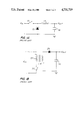
- FIG. 1A is a simplified schematic diagram of a conventional buck regulator
- FIG 1B is a simplified schematic diagram of a conventional flyback regulator
- FIG. 2A is a schematic diagram of a first embodiment of the switching regulator circuit of the present invention which converts a positive input voltage to a lower positive regulated output voltage;
- FIG. 2B is a schematic diagram of a second embodiment of the switching regulator circuit of the present invention which converts a negative input voltage to a lower negative output voltage
- FIG. 3 is a detailed schematic diagram of of the switching regulator of the present invention which converts a positive input voltage to a lower positive output voltage.
- FIGS. IA and lB are simplified drawings of, respectively, conventional buck and flyback switching voltage regulators.
- switch 10 is connected to one end of inductive element 14, the other end of which is connected to output terminal V OUT .
- the cathode of steering diode 12 is also connected to inductor 14 and switch 10 .
- storage capacitor 16 is connected between V OUT and ground.
- the buck regulator of FIG. 1A operates in a well known manner by delivering current to inductor 14 each time switch 10 is closed.
- switch 10 When switch 10 is closed, a current passes through inductor 14. That current, which increases linearly over time because of the inductor, is supplied to the load. Current thus flows through a loop including switch 10, inductor 14 and the load. While switch 10 is closed, current does not pass through diode 12 because diode 12 is back-biased.
- switch 10 is opened, current ceases to pass through switch 10. Instead, inductor 14 discharges energy which had been stored in it while switch 10 was closed in the form of a current to the load. With switch 10 open, diode 12 is forward biased, and a current flows through a loop defined by inductor 14, the load connected to V OUT , and diode 12.
- one end of switch 20 is connected to one end of the primary winding of transformer 22.
- Transformer 22 has a primary to secondary turns ratio of 1:N, with the primary and secondary windings oppositely polarized as indicated by the dots.
- the other ends of switch 20 and the primary winding of transformer 22 are connected to the input supply.
- the secondary winding of transformer 22 is connected to a circuit comprised of diode 24 connected in series with capacitor 26.
- the output of the flyback regulator, V OUT is taken from the node between diode 24 and capacitor 26.
- the flyback regulator of FIG. 1B operates in a well known manner by delivering current to a load connected to V OUT when switch 20 is open.
- switch 20 When switch 20 is closed, current flows through the inductive primary winding of transformer 22, and the winding stores energy. Current is not induced in the secondary winding at this time because diode 24 is back-biased.
- switch 20 When switch 20 is opened, however, energy is transferred from the primary winding to the secondary winding of transformer 22, diode 24 is forward biased, and current flows through a loop defined by diode 24, the load, and secondary winding of transformer 22. Because of the turns ratio, N, of transformer 22, the maximum current provided to V OUT can exceed the current through switch 20.
- That maximum current is determined by the formula: ##EQU1## where I p is the peak switch current, V IN is the input voltage, V OUT is the output voltage, and N is the transformer primary to secondary turns ratio. Output current in the flyback regulator is limited, however, because current is provided to the load only while switch 20 is open.
- the regulator of the present invention provides current to the load both when the switch is opened and when it is closed, thus increasing the maximum current which may be provided to the load.
- switch 101 represents the switch of a switching voltage regulator circuit having switch terminals 102 and 104.
- Switch 101 is turned on and off by switching circuitry 100, shown operatively connected to switch 101 by a dashed line.
- Switching circuitry 100 and switch 101 may be substantially any discrete or integrated circuit switching regulator which allows access to the terminals of the power switching device within the regulator.
- switch 101 and switching circuitry 100 may be implemented using an LT1070 integrated circuit switching regulator manufactured by Linear Technology Corporation of Milpitas, California.
- Terminal 104 of switch 101 is connected to the cathode of diode 106, to one end of capacitor 108, and to output terminal 110 of the circuit.
- the other end of capacitor 108 is connected to ground, to the negative side of voltage source 112 and to terminal T3 of secondary winding 114 of transformer 116.
- Terminal T4 of secondary winding 114 is connected to the anode of diode 106.
- Transformer 116 is a conventional transformer having a turn ratio of primary winding 118 to secondary winding 114 equal to 1/N. Dots 115 and 119 are provided to indicate that the polarity of windings 114 and 118 are opposite.
- Terminal T2 of the primary winding 118 is connected to terminal 102 of switch 101.
- Terminal T1 of primary winding 118 is connected to the positive side of voltage source 112.
- Voltage source 112 has a voltage value equal to V IN .
- Switch 101 has a maximum switch current rating of I MAX .
- turns ratio N a value of 0.25 is given to turns ratio N, although other values of N may be used. If the maximum current rating of switch 101 is 5A, current I OUT delivered to a load can be as high as 5A during the closed condition of switch 101, and as high as 20A during the open condition of switch 101. Total available output current I OUT depends on the switch duty cycle, which in turn is determined by the input voltage V IN and the output voltage V OUT , and by the value of turns ratio N.
- the switching regulator configuration of the present invention unlike conventional buck and flyback configurations, provides current to a load both when the switch is opened and when it is closed.
- V S the maximum switch voltage
- V IN the input voltage
- V S V IN +V OUT (1-N)/N.
- the present invention likewise supplies more output current than a conventional flyback regulator because current flows to the output both when the switch is open and when it is closed.
- the increase in maximum output current of the regulator of the invention is as follows:
- V IN is the supply voltage
- V OUT is the output voltage.
- I OUT /I FLY 1.17, meaning that the maximum output current of the regulator of the invention is 17% greater than that of the flyback regulator.
- Switch 101 represents the switch of a switching voltage regulator having switch terminals 102 and 104, switch 101 being controlled on and off by switching circuitry 100 as described with respect to FIG. 2A.
- Terminal 104 is connected to the negative side of voltage source 112.
- the positive side of voltage source 112 is connected to ground, to terminal T4 of secondary winding 114 of transformer 116 and to one end of capacitor 108.
- Terminal T3 of secondary winding 114 is connected to the cathode of diode 106.
- capacitor 108 is connected to the output terminal 110 of the circuit, to the anode of diode 106, and to terminal T1 of primary winding 118 of transformer 116.
- Terminal T2 of primary winding 118 is connected to the switch terminal 102 of switch 101.
- Transformer 116 is a conventional transformer having a ratio of primary winding 118 to secondary winding 114 equal to 1/N. Dots 115 and 119 are provided to indicate the relative polarity of windings 114 and 118.
- the circuit of FIG. 2B operates in the same manner as described above for the operation of the circuit of FIG. 2A, except that the values of input voltage I IN , input voltage V IN , and output current I OUT are negative.
- a positive output voltage switching regulator of the present invention is shown utilizing an LT1070 integrated circuit switching regulator 300 manufactured by Linear Technology Corporation of Milpitas, Calif.
- Switch 101 drawn in dashed lines, is internal to integrated circuit 300 connected between pin V SW and pin GND of circuit 300.
- Pin V IN is the power input
- pin FB is the feedback pin
- pin V c is the compensation pin of integrated circuit 300.
- Resistor 332 and capacitor 334 connected in series between pin V c and pin GND serve to frequency compensate integrated circuit 300 to prevent oscillations. Further information and details concerning the LT1070 device, and the functions of its pins, may be found in Application Note 19, dated June 1986, entitled “LT1070 Design Manual", published by Linear Technology Corporation.
- Transformer 116 and capacitor 108 are connected to integrated circuit 300 in the manner described with regard to FIG. 2A, above.
- Diode 306 also is connected in the manner of diode 106 of FIG. 2A, except that diode 306 is a Schottky diode.
- a Schottky diode is used because such a diode has a forward voltage drop of only about 0.5V at high current levels, as compared to a conventional diode having a forward drop of 1.8V or more at high currents. By decreasing the voltage dropped across the diode, more voltage is available at the output and the overall efficiency of the regulator is increased.
- the circuit of FIG. 3 further includes series-connected resistor 302 and capacitor 304 connected across the primary winding of transformer 118. Resistor 302 and capacitor 304 together function as a conventional damper circuit to prevent ringing upon the switching off of switch 101. Also connected across the primary winding of transformer 116 are resistor 308 connected in series with diode 312, and capacitor 310 connected in parallel with resistor 308. Resistor 308, capacitor 310 and diode 312 function as a conventional snubber circuit to prevent integrated circuit 300 from becoming damaged by excessive flyback voltage generated by transformer 116 upon turn off of switch 101. Another capacitor 314, connected between pin V IN of integrated circuit 300 and ground, functions to smooth and filter the unregulated voltage V IN .
- operational amplifier 316 which preferably is an LM308 differential amplifier such as is commercially available from Linear Technology Corporation or any of a number of other vendors.
- the output of amplifier 316 is connected to one end of resistor 318, the other end of which is connected to pin FB of integrated circuit 300.
- Capacitor 336 connected between pin FB and V OUT , serves to filter switching spikes from pin FB.
- Capacitor 330 connected between amplifier 316 and V OUT , functions to frequency compensate amplifier 316.
- the level of the output voltage at pin V OUT is established by resistor 320, connected between the output and negative input of amplifier 316, and resistor 322, connected between the negative input of amplifier 316 and ground.
- operational amplifier 316 is to generate a feedback signal, required by integrated circuit 300, which floats above the regulated output at pin V OUT .
- a floating feedback signal is required because the ground pin, GND, of integrated circuit 300, is tied to V OUT , the regulated output, rather than to ground.
- Resistor 338 connected between the positive input of amplifier 316 and V OUT
- resistor 340 connected between the positive input of amplifier 316 and pin GND of integrated circuit 300, function as a Kelvin sensing network between pin V OUT and pin GND of integrated circuit 300.
- Resistors 338 and 340 sense any voltage drop across wire 342 which may occur at high currents, thereby to improve load regulation. Such voltage drop may reach as high as several hundred millivolts, depending on the length and gauge of wire 342. If wire 342 is sufficiently short and of sufficient gauge, resistors 338 and 340 may be eliminated.
- Resistor 336 connected between V OUT and ground, functions to provide a minimum preload on the output of the regulator circuitry to prevent the output voltage from going unregulated high in the event a load were removed from V OUT .
- the circuit of FIG. 3 operates as described with respect to FIG. 2A to provide a regulated voltage output of 5 volts at 10 amps, for a supply voltage V IN of 28 V, when the following parts values are used:
Landscapes
- Engineering & Computer Science (AREA)
- Power Engineering (AREA)
- Dc-Dc Converters (AREA)
Abstract
Description
I.sub.OUT /I.sub.FLY =[NV.sub.IN +V.sub.OUT ]/NV.sub.IN +V.sub.OUT -NV.sub.OUT,
______________________________________
resistor 302:  470          ohms
resistor 308:  470          ohms
resistor 318:  1K           ohms
resistor 320:  1.24K        ohms
resistor 332:  680          ohms
resistor 338:  5K           ohms
resistor 340:  1.24K        ohms
resistor 322:  5K           ohms
resistor 336:  100          ohms
capacitor 312: 0.47         μf
capacitor 304: .002         μf
capacitor 334: 0.33         μf
capacitor 336: 0.01         μf
capacitor 330: 200          μf
capacitor 108: 5000         μf
______________________________________
Claims (5)
Priority Applications (1)
| Application Number | Priority Date | Filing Date | Title |
|---|---|---|---|
| US06/932,715 US4731719A (en) | 1986-11-19 | 1986-11-19 | Current boosted switching regulator |
Applications Claiming Priority (1)
| Application Number | Priority Date | Filing Date | Title |
|---|---|---|---|
| US06/932,715 US4731719A (en) | 1986-11-19 | 1986-11-19 | Current boosted switching regulator |
Publications (1)
| Publication Number | Publication Date |
|---|---|
| US4731719A true US4731719A (en) | 1988-03-15 |
Family
ID=25462786
Family Applications (1)
| Application Number | Title | Priority Date | Filing Date |
|---|---|---|---|
| US06/932,715 Expired - Lifetime US4731719A (en) | 1986-11-19 | 1986-11-19 | Current boosted switching regulator |
Country Status (1)
| Country | Link |
|---|---|
| US (1) | US4731719A (en) |
Cited By (6)
| Publication number | Priority date | Publication date | Assignee | Title |
|---|---|---|---|---|
| US4939632A (en) * | 1989-02-14 | 1990-07-03 | U.S. Philips Corporation | Power supply circuit |
| US5101334A (en) * | 1989-02-14 | 1992-03-31 | U.S. Philips Corporation | High speed power supply circuit with circuit with positive feedback |
| US5383080A (en) * | 1991-07-25 | 1995-01-17 | Hitachi, Ltd. | Semiconductor integrated circuit having voltage limiter circuit |
| US5610804A (en) * | 1994-06-20 | 1997-03-11 | Tdk Corporation | Power supply with dual energy transfer circuits for power factor correction |
| US5847553A (en) * | 1996-09-09 | 1998-12-08 | Sierra Wireless, Inc. | Current booster for PC card |
| WO2003030344A1 (en) * | 2001-10-02 | 2003-04-10 | Somfy S.A.S. | Voltage converter |
Citations (1)
| Publication number | Priority date | Publication date | Assignee | Title |
|---|---|---|---|---|
| DE1591630A1 (en) * | 1967-01-12 | 1970-10-08 | Telefunken Patent | Circuit arrangement for voltage regulation for power supply devices in communications technology, in particular telecommunications technology |
-
1986
- 1986-11-19 US US06/932,715 patent/US4731719A/en not_active Expired - Lifetime
Patent Citations (1)
| Publication number | Priority date | Publication date | Assignee | Title |
|---|---|---|---|---|
| DE1591630A1 (en) * | 1967-01-12 | 1970-10-08 | Telefunken Patent | Circuit arrangement for voltage regulation for power supply devices in communications technology, in particular telecommunications technology |
Non-Patent Citations (2)
| Title |
|---|
| Russ Curtis, "An Inexpensive Switch Mode Power Supply", Motorola Inc., 1973, Figure 1. |
| Russ Curtis, An Inexpensive Switch Mode Power Supply , Motorola Inc., 1973, Figure 1. * |
Cited By (11)
| Publication number | Priority date | Publication date | Assignee | Title |
|---|---|---|---|---|
| US4939632A (en) * | 1989-02-14 | 1990-07-03 | U.S. Philips Corporation | Power supply circuit |
| US5101334A (en) * | 1989-02-14 | 1992-03-31 | U.S. Philips Corporation | High speed power supply circuit with circuit with positive feedback |
| US5383080A (en) * | 1991-07-25 | 1995-01-17 | Hitachi, Ltd. | Semiconductor integrated circuit having voltage limiter circuit |
| US5610804A (en) * | 1994-06-20 | 1997-03-11 | Tdk Corporation | Power supply with dual energy transfer circuits for power factor correction |
| US5847553A (en) * | 1996-09-09 | 1998-12-08 | Sierra Wireless, Inc. | Current booster for PC card |
| WO2003030344A1 (en) * | 2001-10-02 | 2003-04-10 | Somfy S.A.S. | Voltage converter |
| US20040252527A1 (en) * | 2001-10-02 | 2004-12-16 | Bruno Serge | Voltage converter |
| JP2005505225A (en) * | 2001-10-02 | 2005-02-17 | ソムフィ | Voltage converter |
| US7075805B2 (en) | 2001-10-02 | 2006-07-11 | Somfy Sas | Voltage converter with current limiting portion |
| AU2002334320B2 (en) * | 2001-10-02 | 2007-03-22 | Somfy | Voltage converter |
| CN100397764C (en) * | 2001-10-02 | 2008-06-25 | Somfy公司 | Voltage converter |
Similar Documents
| Publication | Publication Date | Title |
|---|---|---|
| US5396412A (en) | Synchronous rectification and adjustment of regulator output voltage | |
| USRE39065E1 (en) | Switching voltage regulator circuit | |
| US6294904B1 (en) | Multiple frequency switching power supply and methods to operate a switching power supply | |
| US4146832A (en) | Constant current series-switching regulator | |
| US4092709A (en) | Multiple output self oscillating converter regulator power supply | |
| US4709323A (en) | Buck-boost parallel resonant converter with inductive energy recovery circuit | |
| EP1998429A2 (en) | Method and apparatus to control two regulated outputs of a flyback power supply | |
| US6671193B1 (en) | Power source and arrangement for restricting the short-circuit current or rectifier | |
| IL34693A (en) | Multiple output dc voltage regulator | |
| US4481565A (en) | Core reset for single-ended dc-to-dc converter | |
| US5517397A (en) | Flyback power converter with spike compensator circuit | |
| JP3475888B2 (en) | Switching power supply | |
| US4608625A (en) | Current driven flyback power supply | |
| US4641229A (en) | Switching DC-to-DC converters | |
| US5103386A (en) | Flyback converter with energy feedback circuit and demagnetization circuit | |
| US8760894B2 (en) | Feedback of output voltage error via current sense winding | |
| US4455596A (en) | Flyback-forward boost switchmode converter | |
| US4731719A (en) | Current boosted switching regulator | |
| US6525434B2 (en) | Binary demand switching circuit | |
| US5831838A (en) | Resonant fly-forward converter circuit | |
| EP0964505B1 (en) | Self-excited DC-DC converter and a power supply device using same | |
| US6205037B1 (en) | Overload protection for a switch mode power supply | |
| JPH05252733A (en) | Power supply generating dc output voltage | |
| US5521808A (en) | Method and circuitry for controlling start-up characteristics of a magnetic amplifier control circuit | |
| SE511444C2 (en) | Procedure for limiting the output current of switched flyback-type power units in overload situations and switched flyback-type power units |
Legal Events
| Date | Code | Title | Description |
|---|---|---|---|
| AS | Assignment |
Owner name: LINEAR TECHOLOGY CORPORATION, 1630 MCCARTHY BLVD., Free format text: ASSIGNMENT OF ASSIGNORS INTEREST.;ASSIGNOR:NELSON, CARL T.;REEL/FRAME:004660/0691 Effective date: 19870113 Owner name: LINEAR TECHOLOGY CORPORATION, A CORP. OF CA., CALI Free format text: ASSIGNMENT OF ASSIGNORS INTEREST;ASSIGNOR:NELSON, CARL T.;REEL/FRAME:004660/0691 Effective date: 19870113 |
|
| STCF | Information on status: patent grant |
Free format text: PATENTED CASE |
|
| CC | Certificate of correction | ||
| REMI | Maintenance fee reminder mailed | ||
| FEPP | Fee payment procedure |
Free format text: PAYOR NUMBER ASSIGNED (ORIGINAL EVENT CODE: ASPN); ENTITY STATUS OF PATENT OWNER: LARGE ENTITY |
|
| FPAY | Fee payment |
Year of fee payment: 4 |
|
| SULP | Surcharge for late payment | ||
| FPAY | Fee payment |
Year of fee payment: 8 |
|
| FPAY | Fee payment |
Year of fee payment: 12 |
|
| AS | Assignment |
Owner name: ANALOG DEVICES INTERNATIONAL UNLIMITED COMPANY, IRELAND Free format text: CHANGE OF NAME;ASSIGNOR:LINEAR TECHNOLOGY LLC;REEL/FRAME:057423/0429 Effective date: 20181105 Owner name: LINEAR TECHNOLOGY LLC, CALIFORNIA Free format text: CHANGE OF NAME;ASSIGNOR:LINEAR TECHNOLOGY CORPORATION;REEL/FRAME:057421/0355 Effective date: 20170502 |