US4649301A - Multiple-input sense amplifier with two CMOS differential stages driving a high-gain stage - Google Patents
Multiple-input sense amplifier with two CMOS differential stages driving a high-gain stage Download PDFInfo
- Publication number
- US4649301A US4649301A US06/689,251 US68925185A US4649301A US 4649301 A US4649301 A US 4649301A US 68925185 A US68925185 A US 68925185A US 4649301 A US4649301 A US 4649301A
- Authority
- US
- United States
- Prior art keywords
- input
- sense amplifier
- channel mos
- gate
- dataline
- Prior art date
- Legal status (The legal status is an assumption and is not a legal conclusion. Google has not performed a legal analysis and makes no representation as to the accuracy of the status listed.)
- Expired - Lifetime
Links
Images


Classifications
-
- H—ELECTRICITY
- H03—ELECTRONIC CIRCUITRY
- H03K—PULSE TECHNIQUE
- H03K5/00—Manipulating of pulses not covered by one of the other main groups of this subclass
- H03K5/01—Shaping pulses
- H03K5/02—Shaping pulses by amplifying
- H03K5/023—Shaping pulses by amplifying using field effect transistors
-
- G—PHYSICS
- G11—INFORMATION STORAGE
- G11C—STATIC STORES
- G11C7/00—Arrangements for writing information into, or reading information out from, a digital store
- G11C7/06—Sense amplifiers; Associated circuits, e.g. timing or triggering circuits
- G11C7/062—Differential amplifiers of non-latching type, e.g. comparators, long-tailed pairs
-
- G—PHYSICS
- G11—INFORMATION STORAGE
- G11C—STATIC STORES
- G11C7/00—Arrangements for writing information into, or reading information out from, a digital store
- G11C7/10—Input/output [I/O] data interface arrangements, e.g. I/O data control circuits, I/O data buffers
- G11C7/1051—Data output circuits, e.g. read-out amplifiers, data output buffers, data output registers, data output level conversion circuits
Definitions
- the field of this invention is directed toward the technology of semiconductor memories, in particular CMOS random access memories (RAMs) and read-only memories (ROMs).
- RAMs CMOS random access memories
- ROMs read-only memories
- bitline and dataline and their symmetrical complementaries receive a signal indicative of the state of a transistor memory cell.
- This state information is transferred from the bitline to the dataline through n-channel pass transistors.
- This state information and its complement are further applied to the inputs of a differential sense amplifier.
- This memory scheme is disadvantageously subject to a V T drop across the bitline, and the sense amplifier is not provided with optimum input voltage levels near the thresholds of the sense amplifier.
- the standard arrangement is further gain-limited, and it tends substantially to delay a signal passing to the dataline.
- the speed of signals passing along the signal path is further detrimentally affected by the relatively high capacitance level of the dataline.
- a p-channel transistor bitline is employed to pull up the bitline and eliminate the V T drop of the bitline, thereby speeding the response time of the circuit.
- the signal to be passed is additionally transferred from the bitline to the dataline by a p-channel transistor.
- the gate of this pass device is controlled by a signal from the complement of the column select signal.
- the dataline pull down n-channel transistor sets the common node voltage of the dataline at a sense amplifier optimum input voltage.
- CMOS differential sense amplifier is constructed with input, differential and high gain stages.
- the input stage has multiple input devices for the dataline and complementary dataline inputs.
- the differential stage is a standard CMOS current mirror differential amplifier.
- the third stage provides both high gain and a high common mode rejection ratio (CMMR).
- CMMR common mode rejection ratio
- the CMOS bitline and dataline sensing scheme and the multi-input sense amplifier are adapted for operation with a CMOS ROM. Accordingly, the arrangement is provided with a complementary dataline and a reference voltage level to supply the inputs of the differential sense amplifier with information regarding the states of the ROM memory cell.
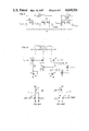
- FIG. 1 shows a CMOS bitline and dataline static RAM scheme of the prior art
- FIG. 2 shows a RAM memory cell including the bitline and dataline scheme of the invention addressed herein;
- FIG. 3 is a small signal equivalent circuit of the bitline and dataline scheme shown in FIG. 2;
- FIG. 4 shows a bias voltage generator circuit effective for supplying the bias level indicated in FIG. 2;
- FIG. 5 is a low impedance dataline representation of the arrangement shown in FIG. 2;
- FIG. 6 is an example of how to reduce the dataline capacitance by reducing the number of pass devices connected to a dataline
- FIG. 7 shows a low capacitance dataline arrangement in which one dataline serves most of the pass transistors and another serves the remaining pass transistors;
- FIG. 8 shows a new high performance multi-input CMOS differential sense amplifier, according to one version of this invention.
- FIGS. 9A and 9B respectively show equivalent circuits of the first and second input stages of the arrangement in FIG. 8;
- FIG. 10 shows the differential and high gain stages of the arrangement shown in FIG. 8;
- FIG. 11 is a small signal equivalent circuit of the amplification stages of the arrangement in FIG. 8;
- FIG. 12 shows a plot of the common mode rejection ratios (CMMR's) of the differential and high gain stages of the arrangement versus the common mode input voltage of the sense amplifier
- FIG. 13 shows a modified multi-input sense amplifier suitable for use in a CMOS ROM.
- FIG. 1 shows a standard CMOS bitline and dataline static RAM scheme which is well known in the art.
- the scheme shows a memory cell 13 with an input row select line (ROWSEL) 15.
- the memory cell 13 has bitline and bitline complement input lines, respectively 19 and 20. These lines 19 and 20 are respectively connected to V CC through pull up n-channel transistors 29 and 30 having gate and source connected electrically.
- Bitlines 19 and 20 are respectively source connected to n-channel pass transistors 31 and 31'.
- Column select (COLSEL) line 32 is connected to the gates of respective pass transistors 31 and 31'.
- At the drain sides of respective pass transistors 31' and 31 are respectively dataline and complementary datalines 33 and 33' connected to the differential inputs of differential sense amplifier 40. These differential inputs are further connected to dataline pull-up transistors respectively 41 and 42.
- FIG. 2 exhibits a CMOS bitline and dataline arrangement according to the invention herein.
- bitline pull-up transistors 29 and 30 bitlines are p-channel instead of n-channel devices.
- the pass transistors 31 and 31' are p-channel and driven at their respective gates by the complementary column select line 32. Again respective datalines 33 and 33' drive the differential inputs to differential amplifier 40.
- the datalines 33 and 33' are provided with n-channel pull-down transistors respectively 42 and 41 which are subject to control at their respective gates by a bias line 55.
- FIG. 4 shows a p-channel CMOS transistor 58 (B1) connected at its gate to ground and at its source to VCC.
- the drain of transistor B1 is connected to the source of a p-channel transistor 59 (B2) also having its gate grounded.
- the node between transistors B1 and B2 is connected to ground through an equivalent one-half memory cell 13' which is gate-driven by signals row select (ROWSEL) or VCC.
- the drain of transistor B2 is in turn connected to the source and gate of n-transistor 60 (B3).
- FIG. 2 eliminates the V T drop of the bitline, which is an improvement over the prior art in FIG. 1. This is accomplished by the pull-up effect of the p-channel transistor on the bitlines 19 and 20. Further, signal transmission is respectively accomplished from bitlines 19 and 20 to datalines 33' and 33 through respective p-channel pass transistors 31 and 31' as indicated in the FIG. 2. As already noted, the gate of pass transistors 31 and 31' is controlled by a signal from the complement of COLSEL instead of the true COLSEL signal. By employing a pull-down n-channel arrangement of transistors 41 and 42 upon the datalines 33' and 33, the common mode dataline voltage is optimally set in accordance with the input voltage requirements of sense amplifier 40. This voltage level is controlled by the gate voltage of transistors 41 and 42, which is BIAS signal 55.
- Pull-up p-channel transistors 29 and 30 operate in the linear region, because their gate-to-source voltages VGS are always greater than their drain to source voltages VDS. Similarly, p-channel pass transistors 31 and 31' are "on", when the complementary COLSEL signal is at ground voltage level.
- FIG. 3 shows the small-signal equivalent circuit of the arrangement shown in FIG. 2. Only the true bit and datalines are shown, because their complementary lines are the same. Transistors 30 and 31' in this Figure are replaced by equivalent resistances Rpullup and Rpass respectively. Bitline and dataline capacitances are respectively represented by the terms Cbitline and Cdataline. Current from memory cell 13 and current through transistor 42 are replaced by the designations Imem and Ipulldown, respectively. Based upon this equivalent circuit, the dataline node voltage Vdat and be determined as follows: ##EQU1## where Vbit is the bitline voltage, Kp is the conduction factor of transistor 31', and Vtp is the p-channel transistor voltage threshold.
- the small signal transresistance of the bitline with respect to memory cell current is thus:
- the small signal transresistance of the dataline with respect to memory cell current can further be determined as follows: ##EQU3##
- the common mode input voltage is the equivalent voltage applied to the sense amplifier when the dataline voltage and its complement are equal. Because the dataline and its complement have an equal voltage swing, the common mode voltage in most cases is at the middle of the voltage swing. This voltage can be set by the BIAS line.
- bias voltage generator circuit is shown in FIG. 4. This voltage is used to drive each of the gates of the dataline pulldown n-channel transistors 41 and 42.
- the voltage level of the BIAS signal is set by the current through pulldown transistor 60 (B3) and the on-resistance of pass transistor 59 (B2) in series with that of pullup transistor 58 (B1) and in parallel with the transistor 13', which produces current equivalent to one half standard memory cell current.
- the current flow through pulldown transistor 60 is mirrored in the dataline transistor 42, since their respective gates are at the same voltage level.
- the dataline voltage is accordingly near the center of the swing range between the dataline maximum and minimum voltages.
- the voltage of the BIAS line can be set almost at any level over V T for a single transistor. This accordingly provides a method to set the common mode input voltage of sense amplifier 40 at an optimum level.
- VCCmin VBIAS+Ipullup (Rpullup) where VBIAS is a voltage greater than V T , Ipullup is the current flow through the pullup transistor and Rpullup is the equivalent on-resistance of the pullup transistor.
- VCC min roughly equal to the bias voltage, and it can be seen that the common mode input voltage to the sense amplifier is always higher than V T when VCC is greater than V T . This insures that operation of the entire circuit is possible at a voltage level greater than V T .
- the voltage gain of the dataline can be sacrificed for the response speed by increasing the output resistance of the pulldown transistor 42. This can be done by biasing the pulldown transistor 42 to operate in its linear region.
- the gate voltage of transistor 42 is thus set higher than the dataline voltage or tied to Vcc.
- the dataline common mode voltage is set by means of the bitline pullup and dataline pulldown with or without the option of an additional dataline pullup transistor, as shown in the lower impedance dataline scheme of FIG. 5.
- Another effective method to speed up the signal path is to reduce the dataline capacitance, which consists of the transistor drain capacitances of all the pass transistors connected to the dataline 33.
- the dataline capacitance which consists of the transistor drain capacitances of all the pass transistors connected to the dataline 33.
- eight datalines 33 for example are provided each serving only eight pass transistors 31' and only one multiple input sense amplifier 40 is employed. If one of the pass devices 31' is turned “on”, the dataline 33 of that entire group will be pulled up to the BIAS voltage level. If none of the eight pass devices 31' are turned on, the datalines 33 of that group will of course remain at Vss and will be pulled down to Vss by a corresponding one of pulldown transistors 42, which have its gate driven by the BIAS line.
- the number of pass transistors 31' which a given dataline 33 can serve can be varied according to the design specification.
- One dataline 33 can serve, for example, a particular selected number of pass transistors 31', while the remaining datalines serve the pass transistors 31' left over. It can be seen that the remaining pass transistors 31 can carry a group of slow path signals, which can be speeded up by being provided with a low capacitance as suggested by the redundance dataline 33" in FIG. 7.
- the speed of a memory chip is of course no faster than its slowest signal path.
- the new scheme according to this invention accordingly provides a technique for improving the speed of the slowest signal path in the memory circuit by reducing the number of parallel datalines on the slowest portion of the signal path.
- a standard differential sense amplifier 40 can clearly be modified to perform as a multi-input sense amplifier 40'.
- the high capacitance created by multiple inputs has a degrading effect upon performance.
- a multiple-input CMOS differential sense amplifier 41' is proposed according to the invention herein employing three stages as shown in FIG. 8. These stages include first and second input stages 71 and 72 respectively, differential stages 73' and a high gain stage 76.
- the input stage 71 and 72 each include multiple input devices such as for example n-channel transistors 79 and 79' for the datalines 33 and their respective complement inputs 33'.
- the low voltage gain of these stages 71 and 72 minimizes the signal delay inherent in the high capacitance which would be caused by a conventional multiple-input sense amplifier 40'.
- the differential stages 73' are standard CMOS current mirror differential amplifiers. All differential signals are handled by n-channel transistor current mirrors 75.
- the high gain stage 76 provides high gain and a high common mode rejection ratio (CMRR) to increase the speed and stability of the arrangement.
- CMRR common mode rejection ratio
- the sense amplifier scheme of FIG. 8 can be used in place of a standard differential sense-amplifier arrangement in any circuit of course with multiple-input stages 71 and 72 either removed or modified to provide only a single input pair of inputs such as 33 and 33'.
- the respective input stages 71 and 72 can be represented by the respective equivalent circuits shown in FIGS. 9A and 9B.
- the input stages 71 and 72 of the sense amplifier 40' are no more than inverters with a p-channel transistor 89', 99' as a load. Since the capacitance of the load is high, a large one of such devices is needed to provide good frequency response and to prevent input n-channel transistors 79 and 79' from getting into a linear operational mode under the influence of high input common mode voltages.
- the differential stage 73' and the high-gain stage are shown in detail in FIG. 10. All of the p-channel transistors are identical, as are the n-channel transistors in the Figure.
- ID3 equals Kp(Vg3-Vtp)**2;
- Vg1 Vcom+v
- IOUT1 kp[ (Vcom+v)**2-(Vcom-v)**2-2Vtp(Vcom+v)+2Vtp(Vcom-v)].
- IOUT1 4kp v(Vcom-Vtp).
- the transconductance of this high gain stage "gmh" follows the relationship: ##EQU6## Further,
- the small signal equivalent circuit of both amplification stages is shown in FIG. 11.
- the node voltage can be calculated as follows; with the transconductances of the p- and n-channel transistors being referred to as gmp and gmn, and the respective output conductances being gop and gon Thus, ##EQU7##
- the current output IOUT1 follows the relationship:
- the voltage gain of the differential stage is:
- VOUT The voltage output of the high gain stage "VOUT" is: ##EQU11##
- IOUT2 can be calculated accordingly:
- the voltage gain of the high gain stage is:
- the voltage gain of the high gain stage is thus very large even with low output resistance and transistor transconductance.
- the common mode output voltage of the two output nodes V2 and VOUT is equal to V1, because all n-channel transistors have the same Vgs in the common mode. This is also true with the p-channel transistors.
- the common mode gain (Acom) is:
- CMRR1 common mode rejection ratio
- CMRR2 common mode rejection ratio of the high gain stage
- FIG. 12 shows this relationship by plotting the CMRR versus common mode input voltages of the sense amplifier.
- CMOS bitline and dataline sensing scheme according to this invention and the multi-input sense amplifier described above can also be successfully used in a CMOS ROM as suggested in FIG. 13.
- the bitline and dataline in this ROM arrangement are essentially identical to the one described earlier with respect to a static RAM memory array.
- ROM memory circuits lack a complementary dataline for connection to one side of a differential sense amplifier, a reference voltage level is needed for the sense amplifier to differentiate the two stages of the memory cell.
- the BIAS voltage level in FIG. 13 is accordingly set at the middle of the maximum voltage swing of the dataline as shown in FIG. 4.
- Capacitor 89 is added to the reference input side to minimize input-stage capacitance loading mismatch, thus reducing the effect of noise from the power supply.
Abstract
Description
DVbit/dImem=Rpullup
gmh=2kp(Vg5-Vtp)+2Akn(Vg6-Vtn);
gmh=(gm p-channel)+A(gm n-channel).
V2=Vdif [gmp(Rout p-channel//Rout n-channel)].
IOUT1=V2/Rout=(Vdif)(gm p-channel)
GAIN1=V2/Vdif=(gmp)(Rout)
VOUT=[(Vin)(gmp)+(GAIN1)(Vin)(gmn)][(Rout p-channel//(Rout n-channel)];
VOUT=Vin (gmp+GAIN 1 gmn)(Rout).
IOUT2=VOUT/Rout=VDIF/2[gmp+GAIN1(gmn)]
GAIN2=VOUT/Vin=[(gmp+(GAIN1)(gmn)]Rout
GAIN2=[(gmp)+(gmp)(gmn)(Rout)](Rout)
GAIN2=GAIN1+GAIN1**2
Acom=V1/Vin=gmp/gmn
CMRR1=GAIN1/Acom=(gmn)(Rout)
CMRR2=GAIN2/Acom=(gmn)(Rout)+(gmn Rout)**2
Claims (5)
Priority Applications (1)
| Application Number | Priority Date | Filing Date | Title |
|---|---|---|---|
| US06/689,251 US4649301A (en) | 1985-01-07 | 1985-01-07 | Multiple-input sense amplifier with two CMOS differential stages driving a high-gain stage |
Applications Claiming Priority (1)
| Application Number | Priority Date | Filing Date | Title |
|---|---|---|---|
| US06/689,251 US4649301A (en) | 1985-01-07 | 1985-01-07 | Multiple-input sense amplifier with two CMOS differential stages driving a high-gain stage |
Publications (1)
| Publication Number | Publication Date |
|---|---|
| US4649301A true US4649301A (en) | 1987-03-10 |
Family
ID=24767652
Family Applications (1)
| Application Number | Title | Priority Date | Filing Date |
|---|---|---|---|
| US06/689,251 Expired - Lifetime US4649301A (en) | 1985-01-07 | 1985-01-07 | Multiple-input sense amplifier with two CMOS differential stages driving a high-gain stage |
Country Status (1)
| Country | Link |
|---|---|
| US (1) | US4649301A (en) |
Cited By (20)
| Publication number | Priority date | Publication date | Assignee | Title |
|---|---|---|---|---|
| US4808857A (en) * | 1986-05-30 | 1989-02-28 | Texas Instruments Incorporated | Sense amplifier circuit for switching plural inputs at low power |
| US4841175A (en) * | 1987-01-23 | 1989-06-20 | Siemens Aktiengesellschaft | ECL-compatible input/output circuits in CMOS technology |
| EP0449311A2 (en) * | 1990-03-30 | 1991-10-02 | Fujitsu Limited | Signal amplifier circuit and semiconductor memory device using the same |
| US5057718A (en) * | 1990-04-03 | 1991-10-15 | National Semiconductor Corp. | Cmos regenerative sense amplifier with high speed latching |
| US5068830A (en) * | 1989-05-09 | 1991-11-26 | Advanced Micro Devices | High speed static ram sensing system |
| US5218570A (en) * | 1990-02-23 | 1993-06-08 | Sgs-Thomson Microelectronics S.R.L. | Sense circuit for reading data stored in nonvolatile memory cells |
| US5237534A (en) * | 1989-04-27 | 1993-08-17 | Kabushiki Kaisha Toshiba | Data sense circuit for a semiconductor nonvolatile memory device |
| US5446397A (en) * | 1992-02-26 | 1995-08-29 | Nec Corporation | Current comparator |
| US5621686A (en) * | 1995-06-07 | 1997-04-15 | Intel Corporation | Multiply and divide current mirror |
| US5783951A (en) * | 1995-10-12 | 1998-07-21 | Rohm Co., Ltd. | Small current detector circuit and locator device using the same |
| DE10146509A1 (en) * | 2001-09-21 | 2003-04-24 | Infineon Technologies Ag | Integrated circuit with input circuit for receiving signals from bus line, has reference voltage adjusted via conduction impedances of conducting transistors |
| US20050017761A1 (en) * | 2001-06-25 | 2005-01-27 | Nanopower Solutions, Inc. | Multi-input differential circuit |
| US20050104633A1 (en) * | 2002-01-23 | 2005-05-19 | Bernd Elend | Transmitter output stage for a two-wire bus |
| US20050172095A1 (en) * | 2004-01-29 | 2005-08-04 | Micron Technology, Inc. | Dual edge command in DRAM |
| US6933752B2 (en) * | 2001-05-31 | 2005-08-23 | International Business Machines Corporation | Method and apparatus for interface signaling using single-ended and differential data signals |
| US20050206424A1 (en) * | 2004-03-16 | 2005-09-22 | Agency For Science, Technology And Research | Current selective D flip-flop circuit |
| US20070097768A1 (en) * | 2005-10-31 | 2007-05-03 | International Business Machines Corporation | System and method for capacitive mis-match bit-line sensing |
| US20100103717A1 (en) * | 2008-10-27 | 2010-04-29 | Seagate Technology Llc | Tuning a variable resistance of a resistive sense element |
| US20120026818A1 (en) * | 2010-07-30 | 2012-02-02 | TW Semiconductor Manufacturing Company, Ltd. | Split Bit Line Architecture Circuits and Methods for Memory Devices |
| US9640231B1 (en) | 2016-02-03 | 2017-05-02 | Qualcomm Incorporated | Shared sense amplifier |
Citations (6)
| Publication number | Priority date | Publication date | Assignee | Title |
|---|---|---|---|---|
| US4342004A (en) * | 1979-05-15 | 1982-07-27 | Tokyo Shibaura Denki Kabushiki Kaisha | Voltage comparator circuit |
| US4375619A (en) * | 1980-06-26 | 1983-03-01 | Bell Telephone Laboratories, Incorporated | FET Operational amplifier with increased output swing |
| US4479202A (en) * | 1979-09-13 | 1984-10-23 | Tokyo Shibaura Denki Kabushiki Kaisha | CMOS Sense amplifier |
| US4504748A (en) * | 1980-10-15 | 1985-03-12 | Fujitsu Limited | Sense amplifier circuit |
| US4507759A (en) * | 1981-02-02 | 1985-03-26 | Hitachi, Ltd | Static memory |
| US4539494A (en) * | 1982-03-30 | 1985-09-03 | Fujitsu Limited | Semiconductor device for use in a sense amplifier |
-
1985
- 1985-01-07 US US06/689,251 patent/US4649301A/en not_active Expired - Lifetime
Patent Citations (6)
| Publication number | Priority date | Publication date | Assignee | Title |
|---|---|---|---|---|
| US4342004A (en) * | 1979-05-15 | 1982-07-27 | Tokyo Shibaura Denki Kabushiki Kaisha | Voltage comparator circuit |
| US4479202A (en) * | 1979-09-13 | 1984-10-23 | Tokyo Shibaura Denki Kabushiki Kaisha | CMOS Sense amplifier |
| US4375619A (en) * | 1980-06-26 | 1983-03-01 | Bell Telephone Laboratories, Incorporated | FET Operational amplifier with increased output swing |
| US4504748A (en) * | 1980-10-15 | 1985-03-12 | Fujitsu Limited | Sense amplifier circuit |
| US4507759A (en) * | 1981-02-02 | 1985-03-26 | Hitachi, Ltd | Static memory |
| US4539494A (en) * | 1982-03-30 | 1985-09-03 | Fujitsu Limited | Semiconductor device for use in a sense amplifier |
Non-Patent Citations (2)
| Title |
|---|
| Chan, "Bit-Select Sense Amplifier"; IBM-TDB; vol. 24, No. 11A, pp. 5654-5656; 4/1982. |
| Chan, Bit Select Sense Amplifier ; IBM TDB; vol. 24, No. 11A, pp. 5654 5656; 4/1982. * |
Cited By (31)
| Publication number | Priority date | Publication date | Assignee | Title |
|---|---|---|---|---|
| US4808857A (en) * | 1986-05-30 | 1989-02-28 | Texas Instruments Incorporated | Sense amplifier circuit for switching plural inputs at low power |
| US4841175A (en) * | 1987-01-23 | 1989-06-20 | Siemens Aktiengesellschaft | ECL-compatible input/output circuits in CMOS technology |
| US5237534A (en) * | 1989-04-27 | 1993-08-17 | Kabushiki Kaisha Toshiba | Data sense circuit for a semiconductor nonvolatile memory device |
| US5068830A (en) * | 1989-05-09 | 1991-11-26 | Advanced Micro Devices | High speed static ram sensing system |
| USRE36579E (en) * | 1990-02-23 | 2000-02-22 | Sgs-Thomson Microelectronics S.R.L. | Sense circuit for reading data stored in nonvolatile memory cells |
| US5218570A (en) * | 1990-02-23 | 1993-06-08 | Sgs-Thomson Microelectronics S.R.L. | Sense circuit for reading data stored in nonvolatile memory cells |
| EP0449311A2 (en) * | 1990-03-30 | 1991-10-02 | Fujitsu Limited | Signal amplifier circuit and semiconductor memory device using the same |
| EP0449311A3 (en) * | 1990-03-30 | 1992-08-05 | Fujitsu Limited | Signal amplifier circuit and semiconductor memory device using the same |
| US5321659A (en) * | 1990-03-30 | 1994-06-14 | Fujitsu Limited | Signal amplifier circuit and semiconductor memory device using the same |
| US5057718A (en) * | 1990-04-03 | 1991-10-15 | National Semiconductor Corp. | Cmos regenerative sense amplifier with high speed latching |
| US5446397A (en) * | 1992-02-26 | 1995-08-29 | Nec Corporation | Current comparator |
| US5621686A (en) * | 1995-06-07 | 1997-04-15 | Intel Corporation | Multiply and divide current mirror |
| US5783951A (en) * | 1995-10-12 | 1998-07-21 | Rohm Co., Ltd. | Small current detector circuit and locator device using the same |
| US6933752B2 (en) * | 2001-05-31 | 2005-08-23 | International Business Machines Corporation | Method and apparatus for interface signaling using single-ended and differential data signals |
| US20050017761A1 (en) * | 2001-06-25 | 2005-01-27 | Nanopower Solutions, Inc. | Multi-input differential circuit |
| DE10146509C2 (en) * | 2001-09-21 | 2003-07-31 | Infineon Technologies Ag | Integrated circuit with an input circuit |
| DE10146509A1 (en) * | 2001-09-21 | 2003-04-24 | Infineon Technologies Ag | Integrated circuit with input circuit for receiving signals from bus line, has reference voltage adjusted via conduction impedances of conducting transistors |
| US20050104633A1 (en) * | 2002-01-23 | 2005-05-19 | Bernd Elend | Transmitter output stage for a two-wire bus |
| US20090248970A1 (en) * | 2004-01-29 | 2009-10-01 | Choi Joo S | Dual edge command |
| US20050172095A1 (en) * | 2004-01-29 | 2005-08-04 | Micron Technology, Inc. | Dual edge command in DRAM |
| US9767886B2 (en) | 2004-01-29 | 2017-09-19 | Micron Technology, Inc. | Memory command received within two clock cycles |
| US9324391B2 (en) | 2004-01-29 | 2016-04-26 | Micron Technology, Inc. | Dual event command |
| US7299329B2 (en) | 2004-01-29 | 2007-11-20 | Micron Technology, Inc. | Dual edge command in DRAM |
| US7549033B2 (en) | 2004-01-29 | 2009-06-16 | Micron Technology, Inc. | Dual edge command |
| US20050206424A1 (en) * | 2004-03-16 | 2005-09-22 | Agency For Science, Technology And Research | Current selective D flip-flop circuit |
| US7286425B2 (en) | 2005-10-31 | 2007-10-23 | International Business Machines Corporation | System and method for capacitive mis-match bit-line sensing |
| US20070097768A1 (en) * | 2005-10-31 | 2007-05-03 | International Business Machines Corporation | System and method for capacitive mis-match bit-line sensing |
| US20100103717A1 (en) * | 2008-10-27 | 2010-04-29 | Seagate Technology Llc | Tuning a variable resistance of a resistive sense element |
| US20120026818A1 (en) * | 2010-07-30 | 2012-02-02 | TW Semiconductor Manufacturing Company, Ltd. | Split Bit Line Architecture Circuits and Methods for Memory Devices |
| US9275721B2 (en) * | 2010-07-30 | 2016-03-01 | Taiwan Semiconductor Manufacturing Company, Ltd. | Split bit line architecture circuits and methods for memory devices |
| US9640231B1 (en) | 2016-02-03 | 2017-05-02 | Qualcomm Incorporated | Shared sense amplifier |
Similar Documents
| Publication | Publication Date | Title |
|---|---|---|
| US4649301A (en) | Multiple-input sense amplifier with two CMOS differential stages driving a high-gain stage | |
| US7339431B2 (en) | CMOS amplifiers with frequency compensating capacitors | |
| US5764101A (en) | Rail-to-rail input common mode range differential amplifier that operates with very low rail-to-rail voltages | |
| US4697112A (en) | Current-mirror type sense amplifier | |
| US4618785A (en) | CMOS sense amplifier with level shifter | |
| US5754078A (en) | Operational amplifier for class B amplification | |
| US6703871B2 (en) | Amplifier for use in semiconductor integrated circuits | |
| EP0050484B1 (en) | Sense amplifier circuit | |
| US5247479A (en) | Current sensing amplifier for SRAM | |
| US4627031A (en) | CMOS memory arrangement | |
| JP3779341B2 (en) | Semiconductor memory device | |
| EP0748042A1 (en) | Improved current sensing differential amplifier for low voltage operation | |
| US4785259A (en) | BIMOS memory sense amplifier system | |
| US4636988A (en) | CMOS memory arrangement with reduced data line compacitance | |
| JP2756797B2 (en) | FET sense amplifier | |
| US4658160A (en) | Common gate MOS differential sense amplifier | |
| US6327190B1 (en) | Complementary differential input buffer for a semiconductor memory device | |
| US5715204A (en) | Sense amplifier with hysteresis | |
| US5075891A (en) | Memory with a variable impedance bit line load circuit | |
| US4394748A (en) | ROM Column select circuit and sense amplifier | |
| US4541077A (en) | Self compensating ROM circuit | |
| US6597612B2 (en) | Sense amplifier circuit | |
| EP0188956B1 (en) | Cmos rom data select circuit | |
| JPH0680993B2 (en) | Differential amplifier circuit | |
| KR100369123B1 (en) | data output buffer |
Legal Events
| Date | Code | Title | Description |
|---|---|---|---|
| AS | Assignment |
Owner name: UNITED TECHNOLOGIES CORPORATION, HARTFORD, CT., CO Free format text: ASSIGNMENT OF ASSIGNORS INTEREST.;ASSIGNOR:VAN TRAN, HIEP;REEL/FRAME:004355/0632 Effective date: 19841108 |
|
| AS | Assignment |
Owner name: MOSTEK CORPORATION, CARROLLTON, TX. Free format text: ASSIGNMENT OF ASSIGNORS INTEREST.;ASSIGNOR:UNITED TECHNOLOGIES CORPORATION A DE CORP., BY: ROBERT E. GREENSTEIN;REEL/FRAME:004375/0899 Effective date: 19850314 |
|
| STCF | Information on status: patent grant |
Free format text: PATENTED CASE |
|
| AS | Assignment |
Owner name: THOMSON COMPONENTS-MOSTEK CORPORATION Free format text: ASSIGNMENT OF ASSIGNORS INTEREST.;ASSIGNOR:CTU OF DELAWARE, INC., FORMERLY MOSTEK CORPORATION;REEL/FRAME:004810/0156 Effective date: 19870721 |
|
| AS | Assignment |
Owner name: SGS-THOMSON MICROELECTRONICS, INC. Free format text: MERGER;ASSIGNORS:SGS SEMICONDUCTOR CORPORATION, A CORP. OF DE;THOMSON HOLDINGS (DELAWARE) INC., A CORP. OF DE;SGS-THOMSON MICROELECTRONICS, INC. A CORP. OF DE (MERGED INTO);REEL/FRAME:005270/0725 Effective date: 19871224 Owner name: SGS-THOMSON MICROELECTRONICS, INC. Free format text: CHANGE OF NAME;ASSIGNOR:THOMSON COMPONENTS-MOSTEK CORPORATION;REEL/FRAME:005270/0714 Effective date: 19871023 |
|
| FPAY | Fee payment |
Year of fee payment: 4 |
|
| FEPP | Fee payment procedure |
Free format text: PAYOR NUMBER ASSIGNED (ORIGINAL EVENT CODE: ASPN); ENTITY STATUS OF PATENT OWNER: LARGE ENTITY |
|
| FPAY | Fee payment |
Year of fee payment: 8 |
|
| FPAY | Fee payment |
Year of fee payment: 12 |