US4571502A - Full wave rectifier having an operational amplifier - Google Patents
Full wave rectifier having an operational amplifier Download PDFInfo
- Publication number
- US4571502A US4571502A US06/446,865 US44686582A US4571502A US 4571502 A US4571502 A US 4571502A US 44686582 A US44686582 A US 44686582A US 4571502 A US4571502 A US 4571502A
- Authority
- US
- United States
- Prior art keywords
- rectifier
- terminal
- amplifier
- inverting
- output terminal
- Prior art date
- Legal status (The legal status is an assumption and is not a legal conclusion. Google has not performed a legal analysis and makes no representation as to the accuracy of the status listed.)
- Expired - Lifetime
Links
Images
Classifications
-
- G—PHYSICS
- G01—MEASURING; TESTING
- G01R—MEASURING ELECTRIC VARIABLES; MEASURING MAGNETIC VARIABLES
- G01R19/00—Arrangements for measuring currents or voltages or for indicating presence or sign thereof
- G01R19/22—Arrangements for measuring currents or voltages or for indicating presence or sign thereof using conversion of ac into dc
Definitions
- This invention relates to a full wave rectifier suitable for construction in an integrated circuit form.
- a typical example of full wave rectifiers for direct current (DC) to alternate current (AC) conversion is a diode bridge circuit.
- the full wave rectifier relying on the bridge circuit encounters a problem that sufficient rectification cannot be achieved due to the temperature dependency of the forward voltage drop caused by the four diodes of the circuit.
- op-amp another full wave rectifier employing one operational amplifier (op-amp) is described in a paper entitled "Precision Rectification" by D. Bowers, published in the ELECTRONIC ENGINEERING, pp. 71-84, June, 1980.
- the rectifier shown in FIG. 6 on page 77 of the Bowers paper comprises an op-amp A1, a diode D1 connected with the output of the op-amp A1, resistors R 1 and R 2 for setting the gain of the op-amp A1, and a load resistor R L .
- this rectifier still requires one diode D1, responsive to the output of the op-amp A1, for performing the switching operation, there is an appreciable amount of voltage drop across the diode, with an insufficient rectification.
- the use of the diode D1 prevents the manufacture of the entire circuit by an MOS (metal oxide semiconductor) IC technique, resulting in a bulky rectifier.
- An object of the invention is, therefore, to provide a full wave rectifier which is suitable for MOS integration, to achieve a wide range of rectification.
- a full wave rectifier has an input terminal which is supplied with an AC signal and a rectifier output terminal for delivering a rectified DC signal.
- An operational amplifier amplifies the AC signal, the amplifier having an inverting input terminal, a non-inverting input terminal grounded and an output terminal.
- a rectifier gain setting means includes a first resistor which is connected between the inverting input terminal of the amplifier and the rectifier input terminal.
- a second resistor has the same resistance as that of the first resistor and is connected between the inverting input terminal of the amplifier and the rectifier output terminal.
- a depletion type MOS FET responds to the output of the amplifier for performing a switching operation.
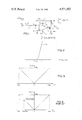
- FIG. 1 is a circuit diagram showing one embodiment of the invention
- FIG. 2 is a graph of a drain current (I D ) vs. gate-source voltage (V GS ) characteristic of an FET used in the embodiment of FIG. 1;
- FIG. 3 is a graph of a rectification characteristic achieved with the embodiment.
- FIG. 4 is a graph showing a rectification characteristic achievable in a prior art rectifier.
- the embodiment includes a rectifier input terminal 1 supplied with an AC voltage; a rectifier output terminal 2 for delivering a rectified DC voltage; an op-amp 8 having an inverting input terminal 3, a non-inverting input terminal 4 which is grounded, and an output terminal 5.
- a depletion type MOS FET 10 responds to the output of the op-amp 8 for performing the switching operation.
- a rectifier gain setting means is provided in the form of resistors 9 and 11.
- a voltage (V GS ) vs. current (I D ) characteristic of the MOS FET 10 clearly indicates that the FET 10 causes a forward voltage drop only when voltage V GS becomes equal to or greater than zero to produce a drain current I D which is equal to or greater than I D1 .
- the FET 10 is operated within the range of voltage negative V GS .
- the gain (or the ratio of the output to input) of the present full wave rectifier is set at "1" by employing the same resistance for the two resistors 9 and 11.
- the op-amp 8 receiver at its terminals 6 and 7, respectively, the operating voltages V DD and V SS shown in FIG. 3 the voltages being supplied from a DC power source (not shown).
- the voltages applied to the terminals 6 and 7 of the op-amp 8 are V DD and V SS , respectively; the input and output voltages of the (FIG. 3) rectifier are V in and V out , respectively; the voltage at a junction 3 between the resistors 9 and 11 is V 1 ; the drain voltage of the MOS FET 10 is V DD ; the resistance of the resistors 9 and 11 is R; and the resistance of a load resistor 12 is R L .
- the output voltage V 2 of the op-amp 8 reaches a corresponding negative level which is smaller than a gate-source voltage (-V TH ) shown in FIG.
- I T is expressed as: ##EQU3## where A is the gain of an op-amp, ⁇ , C ox , W, L, and V T are the charge mobility, gate capacity per unit area, gate width, gate length and threshold voltage of an MOS FET, respectively. It should be noted that equation 3 is applicable to both of the depletion type and enhancement type MOSFETs. Supposing R L >>R, equation (2) may be modified as: ##EQU4##
- equation (4) is rewritten as: ##EQU5##
- Equation (6) teaches that the rectifier of FIG. 1 produces a rectified voltage, at the output terminal 2, which is equal to the input voltage even when the input voltage may be negative.
- the present invention is adaptable to rectify an AC current given as the input to the terminal 1.
- FIG. 4 shows a rectification characteristic which is achievable with the rectifier described in the Bowers paper, previously mentioned.
- V DF the rectified output voltage becomes saturated as the input voltage V in increases beyond the sum (V SS +V DF ) of the negative operating voltage V SS and voltage drop V DF .
- the present invention provides a full wave rectifier suited for the MOS IC fabrication using a depletion type MOS FET to achieve a wider range of rectification.
Landscapes
- Engineering & Computer Science (AREA)
- Power Engineering (AREA)
- Physics & Mathematics (AREA)
- General Physics & Mathematics (AREA)
- Rectifiers (AREA)
- Control Of Electrical Variables (AREA)
- Amplifiers (AREA)
Abstract
Description
V.sub.out =-V.sub.in (6)
Claims (5)
Applications Claiming Priority (2)
| Application Number | Priority Date | Filing Date | Title |
|---|---|---|---|
| JP56197852A JPS5899816A (en) | 1981-12-09 | 1981-12-09 | Rectifying circuit |
| JP56-197852 | 1981-12-09 |
Publications (1)
| Publication Number | Publication Date |
|---|---|
| US4571502A true US4571502A (en) | 1986-02-18 |
Family
ID=16381403
Family Applications (1)
| Application Number | Title | Priority Date | Filing Date |
|---|---|---|---|
| US06/446,865 Expired - Lifetime US4571502A (en) | 1981-12-09 | 1982-12-06 | Full wave rectifier having an operational amplifier |
Country Status (4)
| Country | Link |
|---|---|
| US (1) | US4571502A (en) |
| JP (1) | JPS5899816A (en) |
| CA (1) | CA1196953A (en) |
| DE (1) | DE3245442A1 (en) |
Cited By (7)
| Publication number | Priority date | Publication date | Assignee | Title |
|---|---|---|---|---|
| US5103389A (en) * | 1991-06-11 | 1992-04-07 | Keithley Instruments, Inc. | Frequency range of analog converter by means of external rectifier |
| US5349521A (en) * | 1992-11-25 | 1994-09-20 | Sgs-Thomson Microelectronics, Inc. | Full wave rectifier using a current mirror bridge |
| US5386296A (en) * | 1992-10-28 | 1995-01-31 | Samsung Electronics Co., Ltd. | Chroma burst detection system |
| US5394107A (en) * | 1992-08-27 | 1995-02-28 | Yozan Inc. | Absolute value circuit |
| WO1996033418A1 (en) * | 1995-04-18 | 1996-10-24 | Tridonic Bauelemente Gmbh | Rectifier circuit |
| US6324084B1 (en) * | 1998-12-02 | 2001-11-27 | Seiko Epson Corporation | Power supply device, power supply method, portable electronics apparatus, and electronic timepiece |
| US6750702B2 (en) | 2001-12-21 | 2004-06-15 | International Business Machines Corporation | Limiting amplifier |
Citations (1)
| Publication number | Priority date | Publication date | Assignee | Title |
|---|---|---|---|---|
| US3958170A (en) * | 1974-05-21 | 1976-05-18 | Joseph Lucas Limited | Full wave rectifiers |
Family Cites Families (8)
| Publication number | Priority date | Publication date | Assignee | Title |
|---|---|---|---|---|
| US3723763A (en) * | 1971-08-02 | 1973-03-27 | Bell Telephone Labor Inc | Quasi-rms measurement circuit utilizing field effect transistor as a switch |
| US4097767A (en) * | 1977-01-17 | 1978-06-27 | Dbx, Incorporated | Operational rectifier |
| DE2801684C3 (en) * | 1978-01-16 | 1980-10-09 | Siemens Ag, 1000 Berlin Und 8000 Muenchen | Measuring circuit for determining the size of signal alternating voltages |
| GB1602804A (en) * | 1978-05-16 | 1981-11-18 | Eddystone Radio | Rectifiers |
| JPS5952632B2 (en) * | 1978-07-06 | 1984-12-20 | 日本電信電話株式会社 | rectifier |
| JPS5619383A (en) * | 1979-07-23 | 1981-02-24 | Fujitsu Ltd | Full-wave rectifying system |
| JPS5622966A (en) * | 1979-07-31 | 1981-03-04 | Fujitsu Ltd | Diode rectifying circuit |
| JPS5646666A (en) * | 1979-09-25 | 1981-04-27 | Toshiba Corp | All wave rectifier circuit |
-
1981
- 1981-12-09 JP JP56197852A patent/JPS5899816A/en active Pending
-
1982
- 1982-12-06 US US06/446,865 patent/US4571502A/en not_active Expired - Lifetime
- 1982-12-08 DE DE19823245442 patent/DE3245442A1/en active Granted
- 1982-12-08 CA CA000417242A patent/CA1196953A/en not_active Expired
Patent Citations (1)
| Publication number | Priority date | Publication date | Assignee | Title |
|---|---|---|---|---|
| US3958170A (en) * | 1974-05-21 | 1976-05-18 | Joseph Lucas Limited | Full wave rectifiers |
Non-Patent Citations (8)
| Title |
|---|
| "Applications of MOSFET's in Microelectronics", by R. D. Lohman, Solid State Technology, 3/1966, pp. 23-29. |
| "Designing with Operational Amplifiers", by Jerald Graeme, McGraw-Hill, 1977, chapter 5. |
| Applications of MOSFET s in Microelectronics , by R. D. Lohman, Solid State Technology, 3/1966, pp. 23 29. * |
| Designing with Operational Amplifiers , by Jerald Graeme, McGraw Hill, 1977, chapter 5. * |
| Electronic Engineering, Jun. 1980, "Precision Rectification", by D. Bowers, pp. 71-84. |
| Electronic Engineering, Jun. 1980, Precision Rectification , by D. Bowers, pp. 71 84. * |
| MOS Field Effect Transistors and Integrated Circuits, 1973, by Paul Richman. * |
| MOS Field-Effect Transistors and Integrated Circuits, 1973, by Paul Richman. |
Cited By (8)
| Publication number | Priority date | Publication date | Assignee | Title |
|---|---|---|---|---|
| US5103389A (en) * | 1991-06-11 | 1992-04-07 | Keithley Instruments, Inc. | Frequency range of analog converter by means of external rectifier |
| US5394107A (en) * | 1992-08-27 | 1995-02-28 | Yozan Inc. | Absolute value circuit |
| US5386296A (en) * | 1992-10-28 | 1995-01-31 | Samsung Electronics Co., Ltd. | Chroma burst detection system |
| US5349521A (en) * | 1992-11-25 | 1994-09-20 | Sgs-Thomson Microelectronics, Inc. | Full wave rectifier using a current mirror bridge |
| US5477171A (en) * | 1992-11-25 | 1995-12-19 | Sgs-Thomson Microelectronics, Inc. | Full wave rectifier using current mirror bridge |
| WO1996033418A1 (en) * | 1995-04-18 | 1996-10-24 | Tridonic Bauelemente Gmbh | Rectifier circuit |
| US6324084B1 (en) * | 1998-12-02 | 2001-11-27 | Seiko Epson Corporation | Power supply device, power supply method, portable electronics apparatus, and electronic timepiece |
| US6750702B2 (en) | 2001-12-21 | 2004-06-15 | International Business Machines Corporation | Limiting amplifier |
Also Published As
| Publication number | Publication date |
|---|---|
| CA1196953A (en) | 1985-11-19 |
| DE3245442A1 (en) | 1983-07-21 |
| JPS5899816A (en) | 1983-06-14 |
| DE3245442C2 (en) | 1988-06-09 |
Similar Documents
| Publication | Publication Date | Title |
|---|---|---|
| US5815027A (en) | Circuit configuration for detecting a load current of a power semiconductor component with a source-side load | |
| US4885477A (en) | Differential amplifier and current sensing circuit including such an amplifier | |
| US4415960A (en) | Line variable overcurrent protection for a voltage conversion circuit | |
| US5512849A (en) | Low power intelligent current source for monitoring a high voltage | |
| JPH05315852A (en) | Current limit circuit and constant voltage source for the same | |
| EP0814395A3 (en) | Overcurrent sensing circuit for power mos field effect transistor | |
| US5086364A (en) | Circuitry for detecting a short circuit of a load in series with an fet | |
| EP0669717A1 (en) | Comparator capable of preventing large noise voltage | |
| EP0621638A1 (en) | Integrated high voltage differential sensor using the inverse gain of high voltage transistors | |
| US5656968A (en) | Circuit arrangement for regulating the load current of a power MOSFET | |
| WO2007049597A1 (en) | Current detection circuit | |
| US4571502A (en) | Full wave rectifier having an operational amplifier | |
| US5079454A (en) | Temperature compensated FET power detector | |
| US3588671A (en) | Precision rectifier with fet switching means | |
| JPH0479002B2 (en) | ||
| KR100580748B1 (en) | Gate biasing arrangement | |
| US4618813A (en) | High efficiency series regulator | |
| US4068140A (en) | MOS source follower circuit | |
| EP0791876A3 (en) | Current mirror circuit and signal processing circuit | |
| US5545972A (en) | Current mirror | |
| US4980584A (en) | Multi-stage wideband successive detection logarithmic amplifier | |
| EP0175853A2 (en) | Rectifier circuit | |
| US4072890A (en) | Voltage regulator | |
| US3454850A (en) | Dual mos-fet chopper-summer circuit in a closed loop servo | |
| US4639617A (en) | Variable-bias circuit with HF transmission path |
Legal Events
| Date | Code | Title | Description |
|---|---|---|---|
| AS | Assignment |
Owner name: NIPPON TELEGRAPH & TELEPHONE PUBLIC CORPORATION, 1 Free format text: ASSIGNMENT OF ASSIGNORS INTEREST.;ASSIGNORS:KIMURA, TADAKATSU;MAKABE, TAKAYOSHI;KURAISHI, YOSHIAKI;REEL/FRAME:004075/0469 Effective date: 19821201 Owner name: NIPPON ELECTRIC CO. LTD., 33-1, SHIBA GOCHOME, MIN Free format text: ASSIGNMENT OF ASSIGNORS INTEREST.;ASSIGNORS:KIMURA, TADAKATSU;MAKABE, TAKAYOSHI;KURAISHI, YOSHIAKI;REEL/FRAME:004075/0469 Effective date: 19821201 |
|
| AS | Assignment |
Owner name: NIPPON TELEGRAPH & TELEPHONE CORPORATION Free format text: CHANGE OF NAME;ASSIGNOR:NIPPON TELEGRAPH AND TELEPHONE PUBLIC CORPORATION;REEL/FRAME:004454/0001 Effective date: 19850718 |
|
| STCF | Information on status: patent grant |
Free format text: PATENTED CASE |
|
| FEPP | Fee payment procedure |
Free format text: PAYOR NUMBER ASSIGNED (ORIGINAL EVENT CODE: ASPN); ENTITY STATUS OF PATENT OWNER: LARGE ENTITY |
|
| FPAY | Fee payment |
Year of fee payment: 4 |
|
| FPAY | Fee payment |
Year of fee payment: 8 |
|
| FPAY | Fee payment |
Year of fee payment: 12 |