BACKGROUND OF THE INVENTION
(1) Field of the Invention
The present invention relates to a method and device for controlling the phase of a timing signal and, more particularly, to a method and device for providing by digital processing a timing signal having a predetermined phase relationship with a timing signal component which is extracted from a received, modulated signal in a data modem and the like.
(2) Description of the Prior Art
When a signal modulated in phase shift keying (PSK) modulation or quadrature modulation is received to retrieve the original signal or data by demodulation, it is necessary to extract a timing signal component from the received signal and drive the demodulation circuit by a timing pulse signal having a certain phase relationship with the timing signal component.
Recently, demodulators are changing from the conventional analog circuit arrangement to the digital circuit arrangement, and in order for the digital circuit to perform the above-mentioned timing pulse signal phase control, the timing pulse signal of the digital circuit needs to match the sampled phase of the timing signal component.
In the conventional method for the timing signal phase control by a digital circuit, the timing signal component is extracted from the received, modulated signal and sampled at a certain sampling frequency, the phase of zero level or near-zero level of the thus sampled timing signal component is detected, and the phase of the timing pulse signal is controlled so that the timing pulse signal of the signal processing circuit is timed to the zero-cross point of the sampled timing signal component. In other words, phase control is performed such that the sampling point of time coincides with the zero-cross point of the extracted timing signal component.
However, in terms of the relation between the frequency of the modulated signal and the frequency of the timing pulse signal for the signal processing circuit constituting a demodulator, there are some cases where a certain phase difference must exist between the zero-cross point of the timing signal component and the sampling point. In dealing with these cases by the conventional method which matches the zero-cross point to the sampling point, it is necessary to use a very high sampling frequency or perform interpolation between sampling points. However, the digital processing circuit carries out the process at every sampling of data, and it is undesirable to increase the sampling frequency. This is particularly the case where a microprocessor with a limited processing speed is employed. Interpolation is also undesirable, since it requires much digital processing.
SUMMARY OF THE INVENTION
Accordingly, it is an object of the present invention to realize the method of controlling the phase of a timing signal with a certain phase difference between the zero-cross point of the extracted timing signal and the timing signal of the processing circuit or the sampling point thereof without using a higher sampling frequency.
In order to achieve the above-mentioned object, the present invention contemplates to control in digital fashion the timing pulse signal phase in a signal processing circuit by detecting the zero-cross point of the timing signal component in such a way that the timing signal component extracted from a received signal is shifted in phase for a certain value of phase, the zero-cross point of the shifted timing signal component is detected, and phase control is performed so that the timing pulse signal matches the detected zero-cross point.
One preferred embodiment for shifting the timing signal component is to add a sampled signal of the extracted timing signal component multiplied by one constant to a signal of the timing signal component delayed by the sampling period and multiplied by another constant. By setting the constants appropriately, arbitrary phase difference between the sampling point and the zero-cross point can be obtained, and desired timing signal phase control can be performed without using a higher sampling frequency as will be described in the following embodiments.
These and other objects and advantages, the nature of the present invention, and its various features will appear more fully upon consideration of the various illustrative embodiments now to be described in detail in connection with the accompanying drawings.
BRIEF DESCRIPTION OF THE DRAWINGS
FIG. 1 is a systematic block diagram of a phase controller in a modem which employs a method of controlling the timing signal phase according to the present invention.
FIGS. 2 and 4 are signal waveform diagrams explaining the operation of the embodiment.
FIGS. 3, 5, 6, 7 and 8 are block diagrams of a phase shift circuit which constitutes the principal portion of the embodiments.
FIG. 9 is a systematic diagram of a phase shift circuit embodied by using a microprocessor.
FIG. 10 is a flowchart explaining the operation of the arrangement shown in FIG. 9.
DESCRIPTION OF THE PREFERRED EMBODIMENTS
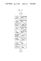
FIG. 1 shows the arrangement of the phase controller in the data modem in accordance with the inventive method of controlling the timing signal phase.
A modulated signal (e.g., as by means of quadrature modulation) received at input terminal 1 is sampled by the first sampling circuit 3 and converted into a digital base band signal by analog-to-digital (A/D) converter and demodulator 4. The base band signal is supplied to a signal processing circuit (not shown) for decoding through automatic equalizer 16 and output terminal 2, and also to timing signal detecting circuit 5. The circuit 5 is constructed by a digital filter having a narrow pass band for extracting timing signal X from the data (information) signal component, and it employs a known circuit such as that disclosed, for example, by L. E. Frank in "Carrier and Bit Synchronization in Data Communication--A tutorial Review", IEEE trans on Comumun. Vol. COM-28, No. 8, Aug. 1980. The extracted timing signal component is fed to phase shift circuit 6. The phase shift circuit 6 constitutes the principal portion for embodying the present invention, receiving the timing signal component and shifting its phase so that the zero-cross point of the timing signal component X is timed to the sampling point of the second sampling circuit 7 which will be mentioned shortly. The circuit 6 will be described in more detail later. The second sampling circuit 7 samples the output signal of the phase shift circuit at the same frequency as that of the timing signal component. Polarity descrimination circuit 8 verifies the polarity of the sampled value in co-operation with bi-level quantization circuit 9 at the same interval as that of the timing signal component so as to convert the phase-shifted signal into a bi-level signal and supplies it to loop filter 11 which provides a control signal for digital VCO 15. A zero output of the loop filter 11 indicates that the zero-cross point of the output of the phase shift circuit 6 matches the sampling point of the second sampling circuit, and a positive or negative output operates on pulse adding/eliminating circuit 13 to add or eliminate a pulse to/from pulses provided by digital pulse generator 14. The resultant pulse outputs are counted down by frequency divider 12, and a timing pulse signal including sampling pulses having a controlled phase is produced. The sampling pulse signal determines the sampling point of the first sampling circuit or the timing for the equalizer 16, and at the same time it is further counted down by frequency divider 10 so as to determine the sampling point of the second sampling circuit 7. In a particular frequency relationship, the timing signal component has a frequency of 1.6 kHz, the pulse generator 14 provides a frequency of 1 MHz, the frequency divider 12 provides the output of 9.6 kHz, and the frequency divider 10 provides the output of 1.6 kHz.
FIG. 3 shows the arrangement of the phase shift circuit 6, in which output signal Xn from the timing signal component detecting circuit 5 is partly multiplied by constant k1 by multiplier 17 and partly delayed by delay element 18 having a delay time T equal to the sampling period and multiplied by constant k2 by multiplier 20. The outputs of the two multipliers are added by adder 19 to form signal Yn.
The sampling signal, namely the sampled timing signal component Xn provided by the sampling circuit 6, is a sinusoidal wave expressed as follows.
X.sub.n =A cos (nωT) (1)
where n is an integer representing the order of sampling, A is a constant, and ω is the angular frequency of the timing signal component.
Similarly, the output Xn+1 from the delay element 18 is expressed as follows.
X.sub.n+1 =A cos {(n+1)ωT} (2)
The output Yn from the adder 19 is expressed as follows. ##EQU1##
Thus the resultant signal is equal to the timing extraction component with its phase shifted by φ. ##EQU2##
Accordingly, by controlling the timing of sampling so that Yn becomes zero by the phase control loop including the polarity discrimination circuit 8, bi-level quantization circuit 9, loop filter 11, pulse adding/eliminating circuit 13, frequency dividers 12 and 10, and second sampling circuit 7, the zero-cross point of the input timing signal component can be set to have a timing relationship with the sampling point being of phase difference φ between contiguous sampling points tn and tn+1 as shown in FIG. 4. The delay time T is determined depending on the sampling frequency, and the desired phase difference φ can be obtained by setting the constants k1 and k2 appropriately. That is to say, in case a system has the zero-cross point out of the sampling point, the phase of the timing pulse signal can be controlled to that phase relationship.
In this embodiment, the delay element is assumed to have a delay time equal to the sampling period T, however, this is not necessary, and the same result is achieved when the delay time is a multiple of the sampling period.
If the first constant k1 is equal to 1, the multiplier 17 becomes unnecessary, allowing the arrangement of FIG. 5. Moreover, if the second constant k2 is equal to 1, or both constants k1 and k2 are equal to 1, arrangement can be made as shown in FIG. 6 or FIG. 7. Matching of the sampling point and the zero-cross point can be achieved by making the second constant k2 equal to 0 in the arrangement of FIG. 3.
FIG. 8 shows another embodiment of the phase shift circuit, wherein the output of the timing signal detecting circuit 5 is sampled by sampling circuits 6-1 and 6-2 in response to the pulses from frequency dividers 10-1 and 10-2 having the same frequency divider, but with a phase difference of T, in place of the delay element used in the embodiment of FIG. 3. Remaining portions with the same reference numbers are the same as those of the foregoing arrangements.
Discrete circuit arrangements for embodying the present invention have been described, however, these digital circuits can be replaced with a signal processor such as a microcomputer for carrying out the foregoing phase shift processes. Such a system arrangement is constructed, as shown in FIG. 9, by connecting through a common bus 21 a microprocessor 22, a RAM 23, a ROM 24, a multiplier 25, and an adder 26, and interfacing the system with the above-mentioned sampling circuit 6 and the polarity discrimination circuit 8 through an input/output circuit (not shown). The arrangement performs the processing as shown in the flowchart of FIG. 10 as follows. The sampled values from the sampling circuit 6 are stored via the input/output circuit into the RAM 23 sequentially at an interval of T or shorter. It will be appreciated that by executing the processes programmed shown in the flowchart at an interval of T seconds for the sampled values Xn+1 and Xn in the RAM 23 and the constants k1 and k2 in the ROM 24, computation for the above equation (3) is carried out at every T seconds. It will further be appreciated that if the microprocessor 22 has a sufficiently high processing speed, the multiplier 25 and adder 26 can be eliminated and their functions can be performed by the software program.
As described in the foregoing embodiments, a sampled signal is phase-shifted merely by performing multiplication and addition, and the zero-cross point of the timing signal component can be set to have a certain phase relationship with the sampling point, whereby the need for a higher sampling frequency is eliminated and the need for a lot of processing for interpolation is also eliminated. Moreover, the method according to the present invention does not cause a degraded performance of phase control which would occur in the conventional system by allowing some phase error when the processing capability is limited.
It is also possible for the present invention to provide the phase relationship with the zero-cross point timed not only between the sampling points Xn and Xn+1, but at any other point by setting the values of constants k1 and k2 in any combination of their polarity.