US4119960A - Method and apparatus for sampling and holding an analog input voltage which eliminates offset voltage error - Google Patents
Method and apparatus for sampling and holding an analog input voltage which eliminates offset voltage error Download PDFInfo
- Publication number
- US4119960A US4119960A US05/767,735 US76773577A US4119960A US 4119960 A US4119960 A US 4119960A US 76773577 A US76773577 A US 76773577A US 4119960 A US4119960 A US 4119960A
- Authority
- US
- United States
- Prior art keywords
- amplifier
- voltage
- input
- sample
- output
- Prior art date
- Legal status (The legal status is an assumption and is not a legal conclusion. Google has not performed a legal analysis and makes no representation as to the accuracy of the status listed.)
- Expired - Lifetime
Links
Images


Classifications
-
- G—PHYSICS
- G11—INFORMATION STORAGE
- G11C—STATIC STORES
- G11C27/00—Electric analogue stores, e.g. for storing instantaneous values
- G11C27/02—Sample-and-hold arrangements
- G11C27/024—Sample-and-hold arrangements using a capacitive memory element
- G11C27/026—Sample-and-hold arrangements using a capacitive memory element associated with an amplifier
-
- H—ELECTRICITY
- H03—ELECTRONIC CIRCUITRY
- H03M—CODING; DECODING; CODE CONVERSION IN GENERAL
- H03M1/00—Analogue/digital conversion; Digital/analogue conversion
- H03M1/12—Analogue/digital converters
- H03M1/124—Sampling or signal conditioning arrangements specially adapted for A/D converters
- H03M1/129—Means for adapting the input signal to the range the converter can handle, e.g. limiting, pre-scaling ; Out-of-range indication
- H03M1/1295—Clamping, i.e. adjusting the DC level of the input signal to a predetermined value
Definitions
- the present invention is directed to a method and apparatus for sampling and holding an analog input voltage which eliminates offset voltage error and more specifically to such a circuit which is especially useful in a 12 bit recirculating Gray code analog to digital converter.
- An analog to digital converter typically includes, especially when it is of the monolithic type, an R-2R resistive ladder network which requires laser trimming.
- an R-2R resistive ladder network which requires laser trimming.
- a 12 bit converter is required there are serious problems with temperature coefficients and lack of automatic zeroing.
- a recirculating converter incorporating a sample and hold circuit is used, the foregoing problem is eliminated.
- problems of offset voltage and common mode voltage errors are then introduced. Manufacturers have attacked this problem by use of transformers which while tending to eliminate offset errors introduce accompanying mechanical and electrical problems.
- such technique requires a zeroing cycle which adds to the time required for conversion.
- Other manufacturers have produced converters where the offset adjustment and/or temperature compensation networks were added along with perhaps a zeroing mode of operation.
- a method of sampling and holding an analog input voltage utilizing a two amplifier sample and hold circuit.
- the output of the first amplifier is connected to an input of the second amplifier.
- the second amplifier forms a Miller integrator and provides a feedback of the stored voltage on the capacitor of the Miller integrator to one input of the first amplifier which is a comparator and which also has the analog input voltage as another input. This other input is compared with the feedback of the stored voltage to produce a correcting output.
- the method comprises sampling and holding the analog voltage by use of the two amplifier sample and hold circuit. Thereafter the analog input voltage from the input of the first amplifier is disconnected and also the output of the first amplifier from the input of the second amplifier is disconnected.
- the first amplifier is converted to an amplifier of predetermined gain by connecting the output to the disconnected input such connection also providing a voltage proportional to said stored voltage.
- FIGS. 1A through 1C illustrate different prior art sample and hold circuits
- FIG. 2 is a sample and hold circuit embodying the present invention
- FIG. 2A is a schematic circuit of a modification of FIG. 2;
- FIG. 3 is a sample and hold circuit embodying the present invention which is especially useful in a recirculating analog to digital converter of the Gray code type;
- FIG. 4 is a detailed circuit schematic of a Gray code type analog to digital converter
- FIG. 5 shows the switching sequence of the switches of FIG. 4 to provide the 12 bit conversion.
- FIG. 1A shows the most common type of sample and hold circuit where when the switch S is closed the capacitor C charges to the sample voltage. The stored voltage is in error by the amount of the offset voltage.
- the circuit of FIG. 1B is another prior art technique where the sample voltage is stored in capacitor C with switches S 2 and S 3 closed.
- the amplifier offset voltage is stored on C. Opening S 2 and S 3 and closing S 1 allows the amplifier to be used as a comparator with the V known voltage and here the compare output has effectively subtracted the offset voltage which was stored on the capacitor.
- an accurate comparison can be made the circuit does not allow the stored voltage to be used as a voltage source which accurately represents the original sample.
- FIG. 1C shows a third prior art technique which is a two stage or two amplifier sample and hold circuit. As in the technique of FIG. 1B an accurate comparison can be made but the stored voltage still contains the offset voltage of amplifier A1 as an error.
- the circuit of FIG. 1C includes the amplifier A2 which is in essence a Miller integrator with the capacitor C connected between its output and its inverting input.
- the noninverting input is grounded.
- the output of amplifier A2 is also connected to the noninverting input of amplifer A1 which compares the voltage being stored on capactor C with switch S closed to the sample voltage which is on the inverting input of amplifier A1.
- a lack of comparison produces a correcting output which is transferred through closed switch S to produce a final stored voltage in capacitor C equal to the sample voltage plus the offset of amplifier A1.
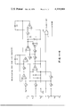
- the circuit of FIG. 2 incorporates the improved technique of the present invention and includes all of the elements of FIG. 1C.
- a switch S 1 which disconnects the sample voltage from amplifier A1 and an additional feedback loop 11 including the switch S 2 between the output of amplifier A1 and its inverting input.
- This converts amplifier A1 when switch S 2 is closed to a unity gain amplifier which provides at its output designated V OUTPUT a voltage exactly equal to the sample voltage without any offset error.
- the offset error of amplifier A1 is effectively subtracted out.
- the sample voltage is initially stored on capacitor C by closure of switches S 1 and S, S 2 being open. Next, S 1 and S are opened and S 2 closed the stored voltage on capacitor C being inputed to the plus terminal of A1.
- the offset voltage is subtracted at the minus terminal due to the feedback through S 2 from the output of amplifier A1.
- This feedback connection thus provides an output voltage which is identically equal to the sample voltage. If it is desired to compare the sample voltage with a known voltage, V KNOWN this can be added at the interconnection 11 as shown by the dashed line and switch S 4 .
- FIG. 2A shows a compensating circuit where instead of grounding the plus terminal of amplifier A2 it is biased with an adjustable pedestal voltage which is selected to compensate for the pedestal added by the switch S. This is connected to the plus terminal of amplifier A2 and thus subtracts from any pedestal voltage added to capacitor C. Switches S and S 3 are closed concurrently.
- FIG. 3 illustrates a sample and hold circuit similar to FIG. 2 but where the interconnecting circuit 11' connecting the output of amplifier A1 to the inverting input is a resistive bridge R 1 , R 2 where R 1 is supplied by a reference voltage V REF .
- R 1 is supplied by a reference voltage V REF .
- V REF reference voltage
- V i is normally an absolute value
- the sample and hold circuit of FIG. 3 when used in a Gray code type analog to digital converter must have positive and negative reference voltages which will keep the result within the bounds of +V R and -V R and the bit complement must be used whenever the result is obtained through the use of a positive reference voltage.
- FIG. 4 illustrates the overall 12 bit converter circuit which incorporates two sample and hold circuits A1, A2 and A4, A5 having respective capacitors C1 and C2. Additional amplifiers A3 and A6 are provided in the associated feedback loops to provide for greater loop gain and therefore increased accuracy; that is especially true for A3.
- the accompanying switching sequence is shown in FIG. 5. Each time the AND gate 12 is strobed it provides one bit of the total of 12 bits.
- the circuit of FIG. 4 does not show the pedestal correction of FIG. 2A which would normally be incorporated.
- the operation of the circuit is as follows.
- state 1 which occurs only on the first bit of the 12 bit sequence the analog input voltage V in is sampled and then stored on the capacitor C1. This includes the offset voltage of A1.
- C2 and the related circuits are held within normal operating conditions.
- state 2 the polarity of the voltage stored on C1 is determined and read out at the logic output. This first bit is normally the sign bit of the 12 bit Gray code.
- A4, A5, C2 portion of the circuit ground voltage is stored on C2 in order to minimize the voltage excursion during state 3. Either a positive or negative voltage may be stored on C2 during the state 3. Storing ground voltage also keeps related circuits active.
- Next state 2 always follows state 4 to determine the polarity of the result and provide the next bit of the Gray code which in this case would be the most significant bit (MSB). Then the process is again continued where in state 3 the typical Gray code equation is calculated. In this calculation the offset voltage in accordance with the invention is subtracted so that the result which is stored in C2 actually does not have the offset voltage and thus there is no cumulative error built up.
- MSB most significant bit
- each of the sample and hold circuits has an accuracy independent of initial amplifier offset voltage or change in offset voltage due to imperfect common mode rejection.
- the first sample and hold circuit provides the necessary multiplication and subtraction to perform the Gray code computation and the second sample and hold circuit temporarily stores the successive computational results and thus form a highly accurate 12 bit circulating analog to digital converter.
- accurate voltage gains of 2.0 and -1.0 are insured by external resistors which can vary greatly in absolute magnitude but can be easily matched to ratio of 1 to 1 to the same accuracy as desired for the overall system. Because of the foregoing feature and in addition the compensation of offset voltage a zeroing mode of operation is not required.
Landscapes
- Engineering & Computer Science (AREA)
- Theoretical Computer Science (AREA)
- Analogue/Digital Conversion (AREA)
Abstract
A sample and hold circuit uses two amplifiers the second being a Miller integrator and the first a comparator which compares the feed back stored capacitor voltage to the sampled voltage to bring the stored voltage of the capacitor to the sample voltage value. This stored voltage will have included in it the offset voltage of the first amplifier. However on readout this offset voltage is eliminated by disconnecting the sample input and also the connection between the output of the first amplifier and the input of the second and instead connecting the output of the first amplifier to the sample input and taking the output from this interconnection line. Since the noninverting or plus terminal of the first amplifier has impressed upon it the stored voltage of the capacitor the unwanted offset voltage is effectively subtracted. The foregoing sample and hold circuit also finds preferred use in a 12 bit recirculating A to D converter where cumulative offset errors would cause error. In such a configuration one of the sample and hold circuits can have the feedback interconnection of the first amplifier configured to perform suitable multiplication and subtraction, for example, for a Gray code. Here a second sample and hold circuit stores successive computational results.
Description
The present invention is directed to a method and apparatus for sampling and holding an analog input voltage which eliminates offset voltage error and more specifically to such a circuit which is especially useful in a 12 bit recirculating Gray code analog to digital converter.
An analog to digital converter typically includes, especially when it is of the monolithic type, an R-2R resistive ladder network which requires laser trimming. When a 12 bit converter is required there are serious problems with temperature coefficients and lack of automatic zeroing. Where a recirculating converter incorporating a sample and hold circuit is used, the foregoing problem is eliminated. However, problems of offset voltage and common mode voltage errors are then introduced. Manufacturers have attacked this problem by use of transformers which while tending to eliminate offset errors introduce accompanying mechanical and electrical problems. In addition, such technique requires a zeroing cycle which adds to the time required for conversion. Other manufacturers have produced converters where the offset adjustment and/or temperature compensation networks were added along with perhaps a zeroing mode of operation.
In a 12 bit converter if, for example, a 2,000 millivolt analog input voltage is being measured, the least significant bit will indicate one-half millivolt and this is thus the required accuracy. Most offset errors begin at 1 to 2 millivolts and increase due to common mode voltages.
It is, therefore, a general object of the present invention to provide an improved sample and hold circuit.
It is another object of the invention to provide a circuit as above which eliminates offset voltage error and common mode errors.
It is another object of the invention to provide a sample and hold circuit which is especially suitable for use in a recirculating type analog to digital converter.
In accordance with the above objects there is provided a method of sampling and holding an analog input voltage utilizing a two amplifier sample and hold circuit. The output of the first amplifier is connected to an input of the second amplifier. The second amplifier forms a Miller integrator and provides a feedback of the stored voltage on the capacitor of the Miller integrator to one input of the first amplifier which is a comparator and which also has the analog input voltage as another input. This other input is compared with the feedback of the stored voltage to produce a correcting output. The method comprises sampling and holding the analog voltage by use of the two amplifier sample and hold circuit. Thereafter the analog input voltage from the input of the first amplifier is disconnected and also the output of the first amplifier from the input of the second amplifier is disconnected. The first amplifier is converted to an amplifier of predetermined gain by connecting the output to the disconnected input such connection also providing a voltage proportional to said stored voltage.
FIGS. 1A through 1C illustrate different prior art sample and hold circuits;
FIG. 2 is a sample and hold circuit embodying the present invention;
FIG. 2A is a schematic circuit of a modification of FIG. 2;
FIG. 3 is a sample and hold circuit embodying the present invention which is especially useful in a recirculating analog to digital converter of the Gray code type;
FIG. 4 is a detailed circuit schematic of a Gray code type analog to digital converter; and
FIG. 5 shows the switching sequence of the switches of FIG. 4 to provide the 12 bit conversion.
FIG. 1A shows the most common type of sample and hold circuit where when the switch S is closed the capacitor C charges to the sample voltage. The stored voltage is in error by the amount of the offset voltage.
The circuit of FIG. 1B is another prior art technique where the sample voltage is stored in capacitor C with switches S2 and S3 closed. In addition, the amplifier offset voltage is stored on C. Opening S2 and S3 and closing S1 allows the amplifier to be used as a comparator with the Vknown voltage and here the compare output has effectively subtracted the offset voltage which was stored on the capacitor. However, although an accurate comparison can be made the circuit does not allow the stored voltage to be used as a voltage source which accurately represents the original sample.
FIG. 1C shows a third prior art technique which is a two stage or two amplifier sample and hold circuit. As in the technique of FIG. 1B an accurate comparison can be made but the stored voltage still contains the offset voltage of amplifier A1 as an error.
More specifically, the circuit of FIG. 1C includes the amplifier A2 which is in essence a Miller integrator with the capacitor C connected between its output and its inverting input. The noninverting input is grounded. The output of amplifier A2 is also connected to the noninverting input of amplifer A1 which compares the voltage being stored on capactor C with switch S closed to the sample voltage which is on the inverting input of amplifier A1. A lack of comparison produces a correcting output which is transferred through closed switch S to produce a final stored voltage in capacitor C equal to the sample voltage plus the offset of amplifier A1.
The circuit of FIG. 2 incorporates the improved technique of the present invention and includes all of the elements of FIG. 1C. However, in addition there is a switch S1 which disconnects the sample voltage from amplifier A1 and an additional feedback loop 11 including the switch S2 between the output of amplifier A1 and its inverting input. This converts amplifier A1 when switch S2 is closed to a unity gain amplifier which provides at its output designated VOUTPUT a voltage exactly equal to the sample voltage without any offset error. The offset error of amplifier A1 is effectively subtracted out. In other words, in the technique of the present invention the sample voltage is initially stored on capacitor C by closure of switches S1 and S, S2 being open. Next, S1 and S are opened and S2 closed the stored voltage on capacitor C being inputed to the plus terminal of A1. The offset voltage is subtracted at the minus terminal due to the feedback through S2 from the output of amplifier A1. This feedback connection thus provides an output voltage which is identically equal to the sample voltage. If it is desired to compare the sample voltage with a known voltage, VKNOWN this can be added at the interconnection 11 as shown by the dashed line and switch S4.
Since the switch S would normally be an MOS field effect transistor having a significant capacitance, the opening of switch S causes a pedestal voltage or a step voltage to be stored on capacitor C and thus introduces error. FIG. 2A shows a compensating circuit where instead of grounding the plus terminal of amplifier A2 it is biased with an adjustable pedestal voltage which is selected to compensate for the pedestal added by the switch S. This is connected to the plus terminal of amplifier A2 and thus subtracts from any pedestal voltage added to capacitor C. Switches S and S3 are closed concurrently.
FIG. 3 illustrates a sample and hold circuit similar to FIG. 2 but where the interconnecting circuit 11' connecting the output of amplifier A1 to the inverting input is a resistive bridge R1, R2 where R1 is supplied by a reference voltage VREF. Here instead of a unity gain amplifier with switch S2 closed it is an operational amplifier capable of doing the multiplication and subtraction as shown by the equation of FIG. 3; that is,
V.sub.OUT = (V.sub.STORED) (R.sub.1 + R.sub.2)/R.sub.1 - V.sub.REF (R.sub.2)/R.sub.1
this equation when R1 is equal to R2, is equivalent to the standard Gray code equation which is
V.sub.i + 1 = V.sub.R - 2V.sub.i
Since in the Gray code Vi is normally an absolute value, the sample and hold circuit of FIG. 3 when used in a Gray code type analog to digital converter must have positive and negative reference voltages which will keep the result within the bounds of +VR and -VR and the bit complement must be used whenever the result is obtained through the use of a positive reference voltage.
FIG. 4 illustrates the overall 12 bit converter circuit which incorporates two sample and hold circuits A1, A2 and A4, A5 having respective capacitors C1 and C2. Additional amplifiers A3 and A6 are provided in the associated feedback loops to provide for greater loop gain and therefore increased accuracy; that is especially true for A3. The accompanying switching sequence is shown in FIG. 5. Each time the AND gate 12 is strobed it provides one bit of the total of 12 bits. The circuit of FIG. 4 does not show the pedestal correction of FIG. 2A which would normally be incorporated.
The operation of the circuit is as follows. In state 1 which occurs only on the first bit of the 12 bit sequence the analog input voltage Vin is sampled and then stored on the capacitor C1. This includes the offset voltage of A1. C2 and the related circuits are held within normal operating conditions. In state 2 the polarity of the voltage stored on C1 is determined and read out at the logic output. This first bit is normally the sign bit of the 12 bit Gray code. In the A4, A5, C2 portion of the circuit, ground voltage is stored on C2 in order to minimize the voltage excursion during state 3. Either a positive or negative voltage may be stored on C2 during the state 3. Storing ground voltage also keeps related circuits active.
In state 3 the Gray code computation is made as indicated. Vin is multiplied by 2 while VR is being subtracted. Polarity of VR is selected to keep the result within the bounds of ±VR. The accuracy is determined by the open loop gain (determined in part by amplifier A3) and the ratio R1 /R2 or R4 /R3. The result of this computation plus the offset voltage is stored on C2.
However, in state 4 the result only is transferred; that is, the result of the foregoing computation as shown in FIG. 5 of ±VR ∓ 2VIN. C1 stores this result plus the offset voltage of A1.
Thus with the device of the present invention as illustrated in FIG. 4, each of the sample and hold circuits has an accuracy independent of initial amplifier offset voltage or change in offset voltage due to imperfect common mode rejection. When coupled together the first sample and hold circuit provides the necessary multiplication and subtraction to perform the Gray code computation and the second sample and hold circuit temporarily stores the successive computational results and thus form a highly accurate 12 bit circulating analog to digital converter. By the use of the algebraic capability of the sample and hold circuit of the present invention accurate voltage gains of 2.0 and -1.0 are insured by external resistors which can vary greatly in absolute magnitude but can be easily matched to ratio of 1 to 1 to the same accuracy as desired for the overall system. Because of the foregoing feature and in addition the compensation of offset voltage a zeroing mode of operation is not required.
Claims (8)
1. A method of sampling and holding an analog input voltage utilizing a two amplifier sample and hold circuit, the output of the first amplifier being connected to an input of the second amplifier, the second amplifier forming a Miller integrator and providing a feedback of the stored voltage on the capacitor of the Miller integrator to one input of the first amplifier which is a comparator and having the analog input voltage as another input which is compared with the feedback of the stored voltage to produce a correcting output, the method comprising the following steps: sampling and holding said analog voltage by use of said two amplifier sample and hold circuit; thereafter disconnecting said analog input voltage from the input of said first amplifier and disconnecting the output of the first amplifier from the input of the second amplifier; and converting said first amplifier to an amplifier of predetermined gain by connecting the output to said disconnected input such connection also providing a voltage proportional to said stored voltage.
2. A method as in claim 1 where said second amplifier includes an inverting input to which said capacitor is connected and the output of said first amplifier and also a non-inverting input and where said disconnection of said first amplifier from the inverting input of the second amplifier produces a pedestal effect said method including the step of biasing said non-inverting input of said second amplifier to compensate for said pedestal.
3. A method as in claim 1 where in said converting step said gain is unity and said voltage at said connection is equal to said stored voltage.
4. Apparatus for sampling and holding an analog input voltage utilzing a two amplifier sample and hold circuit, the output of the first amplifier being connected to an input of the second amplifier, the second amplifier forming a Miller integrator and providing a feedback of the stored voltage on the capacitor of the Miller integrator to one input of the first amplifier which is a comparator and having the analog input voltage as another input which is compared with the feedback of the stored voltage to produce a correcting output, said apparatus comprising means for disconnecting said analog input voltage from the input of said first amplifier and disconnecting the output of the first amplifier from the input of the second amplifier; and means for connecting said output of said first amplifier to its disconnected input.
5. Apparatus as in claim 4 where said means for connecting includes a resistive divider to provide analog multiplication and subtraction.
6. Apparatus as in claim 5 where said analog multiplication and subtraction provides a Gray code function and together with a second said sample and hold circuit for temporarily storing each successive result of the Gray code computation for forming a recirculating analog to digital converter.
7. Apparatus as in claim 4 where said means for connecting forms a feedback loop and includes means for increasing loop gain whereby accuracy is improved.
8. Apparatus as in claim 7 where said means for increasing loop gain includes an amplifier.
Priority Applications (1)
| Application Number | Priority Date | Filing Date | Title |
|---|---|---|---|
| US05/767,735 US4119960A (en) | 1977-02-11 | 1977-02-11 | Method and apparatus for sampling and holding an analog input voltage which eliminates offset voltage error |
Applications Claiming Priority (1)
| Application Number | Priority Date | Filing Date | Title |
|---|---|---|---|
| US05/767,735 US4119960A (en) | 1977-02-11 | 1977-02-11 | Method and apparatus for sampling and holding an analog input voltage which eliminates offset voltage error |
Publications (1)
| Publication Number | Publication Date |
|---|---|
| US4119960A true US4119960A (en) | 1978-10-10 |
Family
ID=25080400
Family Applications (1)
| Application Number | Title | Priority Date | Filing Date |
|---|---|---|---|
| US05/767,735 Expired - Lifetime US4119960A (en) | 1977-02-11 | 1977-02-11 | Method and apparatus for sampling and holding an analog input voltage which eliminates offset voltage error |
Country Status (1)
| Country | Link |
|---|---|
| US (1) | US4119960A (en) |
Cited By (16)
| Publication number | Priority date | Publication date | Assignee | Title |
|---|---|---|---|---|
| US4315253A (en) * | 1979-02-07 | 1982-02-09 | Tytus Hulbert T | Error correction in recirculating remainder analog-to-digital converters |
| US4342983A (en) * | 1980-08-11 | 1982-08-03 | Westinghouse Electric Corp. | Dynamically calibrated successive ranging A/D conversion system and D/A converter for use therein |
| EP0124132A2 (en) * | 1983-05-03 | 1984-11-07 | Racal Data Communications, Inc. | Switched-capacitor circuit analog-to-digital converter |
| US4587443A (en) * | 1984-08-27 | 1986-05-06 | Signetics Corporation | Auto-zero sample and hold circuit |
| US4622536A (en) * | 1984-09-28 | 1986-11-11 | Regents Of The University Of California | Ratio independent cyclic A/D and D/A conversion using a reciprocating reference approach |
| US4672239A (en) * | 1985-05-24 | 1987-06-09 | U.S. Philips Corporation | Sample-and-hold circuit arrangement |
| US4816752A (en) * | 1988-04-07 | 1989-03-28 | Snap-On Tools Corporation | Method and apparatus for low power offset correction of amplified sensor signals |
| US4896156A (en) * | 1988-10-03 | 1990-01-23 | General Electric Company | Switched-capacitance coupling networks for differential-input amplifiers, not requiring balanced input signals |
| US4918450A (en) * | 1988-06-20 | 1990-04-17 | Kabushiki Kaisha Toshiba | Analog/digital converter circuit |
| US5107266A (en) * | 1990-05-12 | 1992-04-21 | Goldstar Electron Co., Ltd. | Algorithmic analog/digital converting circuit |
| US5585756A (en) * | 1995-02-27 | 1996-12-17 | University Of Chicago | Gated integrator with signal baseline subtraction |
| WO1998027654A2 (en) * | 1996-12-16 | 1998-06-25 | Telefonaktiebolaget Lm Ericsson (Publ) | Cyclic analog-to-digital conversion |
| US5798664A (en) * | 1995-04-07 | 1998-08-25 | Nec Corporation | Offset cancelling amplifier circuit having Miller integrator as offset detector |
| US6340903B1 (en) | 2000-05-10 | 2002-01-22 | Zilog, Ind. | Auto-zero feedback sample-hold system |
| US20060284653A1 (en) * | 2005-06-20 | 2006-12-21 | Powen Chen | Method for sample and hold a signal and flat pannel driving method using the same |
| EP2736156A1 (en) * | 2012-11-27 | 2014-05-28 | ST-Ericsson SA | Voltage polarity detection for DCM/CCM boundary detection in DC/DC converters |
Citations (2)
| Publication number | Priority date | Publication date | Assignee | Title |
|---|---|---|---|---|
| US3588881A (en) * | 1969-07-22 | 1971-06-28 | Gordon Eng Co | Cyclic device for analog to digital conversion |
| US3982241A (en) * | 1974-08-19 | 1976-09-21 | Digital Equipment Corporation | Self-zeroing analog-to-digital conversion system |
-
1977
- 1977-02-11 US US05/767,735 patent/US4119960A/en not_active Expired - Lifetime
Patent Citations (2)
| Publication number | Priority date | Publication date | Assignee | Title |
|---|---|---|---|---|
| US3588881A (en) * | 1969-07-22 | 1971-06-28 | Gordon Eng Co | Cyclic device for analog to digital conversion |
| US3982241A (en) * | 1974-08-19 | 1976-09-21 | Digital Equipment Corporation | Self-zeroing analog-to-digital conversion system |
Cited By (21)
| Publication number | Priority date | Publication date | Assignee | Title |
|---|---|---|---|---|
| US4315253A (en) * | 1979-02-07 | 1982-02-09 | Tytus Hulbert T | Error correction in recirculating remainder analog-to-digital converters |
| US4342983A (en) * | 1980-08-11 | 1982-08-03 | Westinghouse Electric Corp. | Dynamically calibrated successive ranging A/D conversion system and D/A converter for use therein |
| EP0124132A2 (en) * | 1983-05-03 | 1984-11-07 | Racal Data Communications, Inc. | Switched-capacitor circuit analog-to-digital converter |
| EP0124132A3 (en) * | 1983-05-03 | 1987-12-02 | Racal Data Communications, Inc. | Switched-capacitor circuit analog-to-digital converter |
| US4587443A (en) * | 1984-08-27 | 1986-05-06 | Signetics Corporation | Auto-zero sample and hold circuit |
| US4622536A (en) * | 1984-09-28 | 1986-11-11 | Regents Of The University Of California | Ratio independent cyclic A/D and D/A conversion using a reciprocating reference approach |
| US4672239A (en) * | 1985-05-24 | 1987-06-09 | U.S. Philips Corporation | Sample-and-hold circuit arrangement |
| US4764689A (en) * | 1985-05-24 | 1988-08-16 | U.S. Philips Corporation | Sample-and-hold circuit arrangement |
| US4816752A (en) * | 1988-04-07 | 1989-03-28 | Snap-On Tools Corporation | Method and apparatus for low power offset correction of amplified sensor signals |
| US4918450A (en) * | 1988-06-20 | 1990-04-17 | Kabushiki Kaisha Toshiba | Analog/digital converter circuit |
| US4896156A (en) * | 1988-10-03 | 1990-01-23 | General Electric Company | Switched-capacitance coupling networks for differential-input amplifiers, not requiring balanced input signals |
| US5107266A (en) * | 1990-05-12 | 1992-04-21 | Goldstar Electron Co., Ltd. | Algorithmic analog/digital converting circuit |
| US5585756A (en) * | 1995-02-27 | 1996-12-17 | University Of Chicago | Gated integrator with signal baseline subtraction |
| US5798664A (en) * | 1995-04-07 | 1998-08-25 | Nec Corporation | Offset cancelling amplifier circuit having Miller integrator as offset detector |
| WO1998027654A2 (en) * | 1996-12-16 | 1998-06-25 | Telefonaktiebolaget Lm Ericsson (Publ) | Cyclic analog-to-digital conversion |
| WO1998027654A3 (en) * | 1996-12-16 | 1998-07-30 | Telfonaktiebolaget Lm Ericsson | Cyclic analog-to-digital conversion |
| US5995035A (en) * | 1996-12-16 | 1999-11-30 | Telefonaktiebolaget Lm Ericsson | Cyclic analog-to-digital converter that reduces the accumulation of offset errors |
| US6340903B1 (en) | 2000-05-10 | 2002-01-22 | Zilog, Ind. | Auto-zero feedback sample-hold system |
| US20060284653A1 (en) * | 2005-06-20 | 2006-12-21 | Powen Chen | Method for sample and hold a signal and flat pannel driving method using the same |
| EP2736156A1 (en) * | 2012-11-27 | 2014-05-28 | ST-Ericsson SA | Voltage polarity detection for DCM/CCM boundary detection in DC/DC converters |
| WO2014083008A1 (en) * | 2012-11-27 | 2014-06-05 | St-Ericsson Sa | Voltage polarity detection for dcm/ccm boundary detection in dc/dc converters |
Similar Documents
| Publication | Publication Date | Title |
|---|---|---|
| US4119960A (en) | Method and apparatus for sampling and holding an analog input voltage which eliminates offset voltage error | |
| EP0169535B1 (en) | Analog to digital converter | |
| US4803462A (en) | Charge redistribution A/D converter with increased common mode rejection | |
| KR100433072B1 (en) | Voltage to current converter for high frequency applications | |
| US7095346B2 (en) | A/D converter with minimized transfer error | |
| EP0849883B1 (en) | Analog-to-digital converter | |
| US4568917A (en) | Capacitive digital to analog converter which can be trimmed up and down | |
| US4315254A (en) | Self-compensating A-D converter | |
| US6031480A (en) | Method and apparatus for implementing a pipelined A/D converter with inter-stage amplifiers having no common mode feedback circuitry | |
| US4622536A (en) | Ratio independent cyclic A/D and D/A conversion using a reciprocating reference approach | |
| CN107959498B (en) | Analog-to-digital converter with offset calibration | |
| US5541599A (en) | Data independent loading of a reference in a discrete time system | |
| US7081785B2 (en) | Comparing circuit and offset compensating apparatus | |
| KR910008523B1 (en) | Sequencial comparator typed analog to digital converter | |
| EP0483846B1 (en) | Analog-to-digital converter circuit | |
| US4975700A (en) | Analog-to-digital converter with non-linear error correction | |
| US6891486B1 (en) | Calibrating capacitor mismatch in a pipeline ADC | |
| JPH10163773A (en) | Current amplifier and current mode a/d converter using the same | |
| JPS5946131B2 (en) | encoding circuit | |
| EP0448328A2 (en) | Digital-to-analog converter having a circuit for compensating for variation in output dependent on temperature change | |
| EP0694924A1 (en) | Differential sample-hold circuit | |
| US6150968A (en) | Trimming circuitry for pipeline A/D converter | |
| US20010009495A1 (en) | Direct-to-digital temperature sensor | |
| US3936759A (en) | Offset reduction apparatus for analog circuits | |
| US5841383A (en) | Current mode track and hold circuit |
Legal Events
| Date | Code | Title | Description |
|---|---|---|---|
| AS | Assignment |
Owner name: INTERNATIONAL RECTIFIER CORPORATION, A DE CORP. Free format text: SECURITY INTEREST;ASSIGNOR:SILICONIX INCORPORATED, A DE CORP.;REEL/FRAME:005562/0082 Effective date: 19901221 |
|
| AS | Assignment |
Owner name: SILICONIX INCORPORATED, A CORP. OF DE Free format text: RELEASE BY SECURED PARTY, RECORDED AT REEL 5562, FRAME 0082, ON 12-28-90;ASSIGNOR:INTERNATIONAL RECTIFIER CORPORATION;REEL/FRAME:005660/0221 Effective date: 19910320 |