US4047220A - Bipolar transistor structure having low saturation resistance - Google Patents
Bipolar transistor structure having low saturation resistance Download PDFInfo
- Publication number
- US4047220A US4047220A US05/644,338 US64433875A US4047220A US 4047220 A US4047220 A US 4047220A US 64433875 A US64433875 A US 64433875A US 4047220 A US4047220 A US 4047220A
- Authority
- US
- United States
- Prior art keywords
- region
- collector
- conductivity type
- regions
- resistance
- Prior art date
- Legal status (The legal status is an assumption and is not a legal conclusion. Google has not performed a legal analysis and makes no representation as to the accuracy of the status listed.)
- Expired - Lifetime
Links
- 239000004065 semiconductor Substances 0.000 claims description 26
- 239000000758 substrate Substances 0.000 claims description 17
- 230000007480 spreading Effects 0.000 claims description 6
- 239000004020 conductor Substances 0.000 claims description 2
- 238000009792 diffusion process Methods 0.000 description 15
- 230000015556 catabolic process Effects 0.000 description 7
- 238000004519 manufacturing process Methods 0.000 description 5
- 238000004804 winding Methods 0.000 description 5
- 238000000034 method Methods 0.000 description 3
- VYPSYNLAJGMNEJ-UHFFFAOYSA-N Silicium dioxide Chemical compound O=[Si]=O VYPSYNLAJGMNEJ-UHFFFAOYSA-N 0.000 description 2
- 230000008901 benefit Effects 0.000 description 2
- 239000002775 capsule Substances 0.000 description 2
- 230000006872 improvement Effects 0.000 description 2
- 238000002955 isolation Methods 0.000 description 2
- 239000000463 material Substances 0.000 description 2
- 230000004048 modification Effects 0.000 description 2
- 238000012986 modification Methods 0.000 description 2
- ZOKXTWBITQBERF-UHFFFAOYSA-N Molybdenum Chemical compound [Mo] ZOKXTWBITQBERF-UHFFFAOYSA-N 0.000 description 1
- XAGFODPZIPBFFR-UHFFFAOYSA-N aluminium Chemical compound [Al] XAGFODPZIPBFFR-UHFFFAOYSA-N 0.000 description 1
- 229910052782 aluminium Inorganic materials 0.000 description 1
- 230000003466 anti-cipated effect Effects 0.000 description 1
- 238000010420 art technique Methods 0.000 description 1
- 238000006243 chemical reaction Methods 0.000 description 1
- 230000001419 dependent effect Effects 0.000 description 1
- 238000010586 diagram Methods 0.000 description 1
- 239000007772 electrode material Substances 0.000 description 1
- 239000011810 insulating material Substances 0.000 description 1
- 229910052750 molybdenum Inorganic materials 0.000 description 1
- 239000011733 molybdenum Substances 0.000 description 1
- 229910021420 polycrystalline silicon Inorganic materials 0.000 description 1
- 230000008569 process Effects 0.000 description 1
- 230000009467 reduction Effects 0.000 description 1
- 235000012239 silicon dioxide Nutrition 0.000 description 1
- 239000000377 silicon dioxide Substances 0.000 description 1
Images
Classifications
-
- H—ELECTRICITY
- H01—ELECTRIC ELEMENTS
- H01L—SEMICONDUCTOR DEVICES NOT COVERED BY CLASS H10
- H01L27/00—Devices consisting of a plurality of semiconductor or other solid-state components formed in or on a common substrate
- H01L27/02—Devices consisting of a plurality of semiconductor or other solid-state components formed in or on a common substrate including semiconductor components specially adapted for rectifying, oscillating, amplifying or switching and having at least one potential-jump barrier or surface barrier; including integrated passive circuit elements with at least one potential-jump barrier or surface barrier
- H01L27/04—Devices consisting of a plurality of semiconductor or other solid-state components formed in or on a common substrate including semiconductor components specially adapted for rectifying, oscillating, amplifying or switching and having at least one potential-jump barrier or surface barrier; including integrated passive circuit elements with at least one potential-jump barrier or surface barrier the substrate being a semiconductor body
- H01L27/08—Devices consisting of a plurality of semiconductor or other solid-state components formed in or on a common substrate including semiconductor components specially adapted for rectifying, oscillating, amplifying or switching and having at least one potential-jump barrier or surface barrier; including integrated passive circuit elements with at least one potential-jump barrier or surface barrier the substrate being a semiconductor body including only semiconductor components of a single kind
- H01L27/082—Devices consisting of a plurality of semiconductor or other solid-state components formed in or on a common substrate including semiconductor components specially adapted for rectifying, oscillating, amplifying or switching and having at least one potential-jump barrier or surface barrier; including integrated passive circuit elements with at least one potential-jump barrier or surface barrier the substrate being a semiconductor body including only semiconductor components of a single kind including bipolar components only
- H01L27/0823—Devices consisting of a plurality of semiconductor or other solid-state components formed in or on a common substrate including semiconductor components specially adapted for rectifying, oscillating, amplifying or switching and having at least one potential-jump barrier or surface barrier; including integrated passive circuit elements with at least one potential-jump barrier or surface barrier the substrate being a semiconductor body including only semiconductor components of a single kind including bipolar components only including vertical bipolar transistors only
- H01L27/0825—Combination of vertical direct transistors of the same conductivity type having different characteristics,(e.g. Darlington transistors)
Landscapes
- Engineering & Computer Science (AREA)
- Power Engineering (AREA)
- Physics & Mathematics (AREA)
- Condensed Matter Physics & Semiconductors (AREA)
- General Physics & Mathematics (AREA)
- Computer Hardware Design (AREA)
- Microelectronics & Electronic Packaging (AREA)
- Bipolar Transistors (AREA)
- Bipolar Integrated Circuits (AREA)
Abstract
A triple diffused interdigitated NPN transistor formed in an isolated N-epitaxial pocket of an otherwise standard NPN bipolar junction isolated integrated circuit. The N-type diffused collector pocket in the N-epitaxial layer lowers collector resistance of the triple diffused NPN device.
Description
The present invention relates to semiconductor devices and more particularly to monolithic integrated circuit structures including bipolar semiconductor devices some of which are characterized by a high voltage collector-to-base breakdown capability and others of which are characterized by a low voltage breakdown capability, but with low saturation resistance characteristics.
The fabrication of semiconductor devices in monolithic integrated circuit form have provided the circuit designer with a wide range of capabilities in developing electrical circuits useful for performing numerous functions. Generally, however, the fabrication of integrated circuits on a specific resistivity substrate requires compromises in device characteristics where devices of substantially different power or voltage handling capability are required. For example, the requirement for a low saturation voltage drop in a high current, low voltage signal transistor is not easily achieved in an integrated circuit structure including high voltage, high current power transistors, the characteristics of which dictate the type of semiconductor material required for the integrated circuit. For example, where it is desired to fabricate a transistor having a collector-to-base breakdown voltage of approximately 500 volts, it is generally necessary to select a semiconductor substrate having an epitaxial layer formed thereon with a resistivity of at least 10 ohm-cm and a thickness of approximately 45 to 50 microns. On the other hand, if it is desired to construct a semiconductor device having only a 50 volt collector-to-base breakdown voltage, an epitaxial layer of 1 ohm-cm and approximately 10 to 12 microns would provide optimum performance.
Where it is desired to provide both high voltage power devices (i.e., in excess of several hundred volts collector-to-base breakdown voltage) and low voltage signal devices (i.e., less than one hundred volts collector-to-base breakdown voltage) on the same integrated circuit substrate, it is necessary to select a substrate which will meet the more stringent demands of the high voltage, high power device and compromise the characteristics of the low voltage signal device. This compromise device generally includes an unacceptably high collector series resistance which results from the device geometry.
It is therefore an object of this invention to provide on a single monolithic integrated circuit high voltage, high power devices and low voltage signal devices in which the low voltage signal devices are characterized by a low saturation resistance.
It is another object of this invention to provide a bipolar transistor structure having low saturation resistance.
Briefly, in accordance with a preferred embodiment of the invention, a monolithic integrated circuit structure including high voltage power and low voltage signal devices are provided. The low voltage signal devices are characterized by a low saturation resistance which is achieved in accordance with this invention by interdigitated base, collector and emitter regions and wherein the lateral spreading resistance of the collector region underlying the base region is utilized to reduce the collector series resistance.
In practicing the invention, a high resistivity epitaxial layer suitable for the fabrication of high voltage power devices is formed over a substrate and isolation regions are formed from the surface and through the epitaxial layer to the substrate to isolate a portion of the epitaxial layer from other portions of the epitaxial layer. Within the isolated region, a region of lower resistivity than the epitaxial region is formed as the collector region of the device. A plurality of base regions are formed in the collector region and a like plurality of emitter regions are formed in the base regions. Additional collector regions are interdigitated with the plurality of base regions to provide a plurality of current paths between the collector and base regions. These parallel current paths reduce the series collector resistance normally associated with thick collector regions, wide buried layers and deep collector contact diffusions.
These and other objects and advantages of the invention will become more apparent from the following detailed description taken in conjunction with the accompanying drawings in which:
FIG. 1 is an electrical schematic diagram of a typical circuit configuration employing high voltage power and low voltage signal transistors in a high frequency inverter;
FIG. 2 is a perspective view, in partial cross-section of an embodiment of the present invention;
FIG. 3 is a plan view of the embodiment of the invention illustrated in FIG. 2; and
FIG. 4 is a partial sectional view of the embodiment of FIG. 2 illustrating the spreading resistance between alternately spaced collector and base contacts.
Although the semiconductor device of this invention will have many possible applications, one of the presently anticipated applications for this invention is its use in dc/ac inverter applications wherein the inverter operates at a relatively high frequency (e.g., 25 kHz). This high frequency ac output from the inverter would then be used to power an ac load or the output of the inverter can be rectified and filtered appropriately to provide a dc output voltage, if desired.
By way of example, FIG. 1 illustrates a typical inverter circuit in which the semiconductor devices of the present invention may be utilized. Specifically, FIG. 1 illustrates an inverter 10 including high voltage power transistors 11 and 12 with their collector electrodes connected to the primary winding of a transformer 13 which also includes a secondary winding connected to a load 14. The transformer 13 further includes a tertiary winding connected to a control circuit 15 which controls the conduction of transistors 11, 12 and a low voltage signal transistor 16 having its collector electrode connected to the emitter electrodes of the switching transistors. As is typical of many inverters of the type illustrated in FIG. 1, alternate conduction of transistors 11 and 12 causes current flow through the primary winding of the transformer 13 which in turn induces a voltage in the secondary winding for transferring power to the load 14. Since the inverter of FIG. 1 is merely intended to illustrate one of many possible uses of the present invention, no further comments will be made regarding the operation of the inverter.
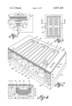
FIG. 2 illustrates an embodiment of the present invention in which a low voltage bipolar transistor 20 includes interdigitated base, emitter and collector electrodes. The bipolar transistor 20 includes a semiconductor substrate 21 of a first conductivity type, such as P-type substrate. An epitaxial layer 22 of a second conductivity type (N-type) is formed on a major surface of the substrate 21. A buried layer 23 of N+ conductivity type is formed at the interface of the substrate 21 and the epitaxial layer 22. Typically, the buried layer 23 is formed by well-known diffusion techniques.
A deep collector contact (or sinker) region 24 of N+ conductivity type extends from the surface and continues through the epitaxial layer 22 and makes contact with the buried layer 23. Also extending from the surface of the epitaxial layer and through the epitaxial layer to the substrate 21 is a P-type region 25 which completely surrounds the collector region (including the buried layer 23 and collector region 24) and isolates this portion of the epitaxial layer 22 from all other portions of the epitaxial layer. Accordingly, the semiconductor device formed within the isolation region or pocket region 26 is electrically separate and apart from other semiconductor devices which may be physically included on the same substrate.
As described above, where high voltage power semiconductor devices are to be fabricated in monolithic integrated circuits, the voltage and current carrying capabilities of the desired device dictate, among other things, the relative thickness of the epitaxial layer and the resistivity thereof. Typically, for a power transistor having a collector-to-base breakdown voltage of 500 volts and approximately 1 ampere current-carrying capability, it is necessary to select a resistivity of approximately 15 ohm-cm and an epitaxial layer thickness of approximately 45 microns. While these parameters are useful in providing high voltage power devices, the fabrication of low voltage signal devices in such an epitaxial layer by prior art techniques would result in the fabrication of a transistor characterized by a high collector series resistance including the bulk collector resistance, the buried layer resistance and the deep collector contact resistance. Hence, the resulting low power signal semiconductor would exhibit high saturation resistance, a clearly undesirable characteristic for a transistor operated in a switching mode, where the high saturation resistance would undesirably increase power losses in the device.
In accordance with the present invention, the aforementioned difficulties are overcome by inclusion of a region of lower resistivity in the isolated pocket region 26. FIG. 2 illustrates this region of lower resistivity by the numeral 31, which depicts the outline of this lower resistivity region which, for example, may be formed by a closed tube or capsule diffusion technique. If it is desired to provide a low cost process, then certain technical considerations may limit the overall effectiveness of this step. For example, these deep diffusions must be weighted against the required low surface concentrations and reasonable diffusion times, including the costs associated with the diffusion times.
By way of specific example, where it is desired to have a single base diffusion step for both power and signal devices, then the surface concentration of region 31 cannot exceed that of the P-type base diffusion chosen for the power device characteristics. Otherwise, type conversion will not occur. The surface concentration value for the P-type base diffusion is typically 1018 atoms/cm3. Hence, the average resistivity near the surface is approximately 0.3 ohm-cm, but increases to the background value of resistivity (i.e., 10-12 ohm-cm). Thus, the average resistivity over the pocket region 31 may be approximately 1 ohm-cm. Also, for similar practical reasons, the depth of pocket region 31 may not extend fully to the buried layer 23. Therefore, under some conditions, there may be a region 27 of uniform resistivity formed by the unmodified epitaxial layer 22.
Within the lower resistivity pocket region 31, a plurality of base regions 32 are formed by P-type diffusion, for example. As illustrated, the P-type base regions 32 are elongated and, as further illustrated in the plan view of FIG. 3, are interconnected by a common P-type region and by an overlying conductive grid 42. A first plurality of N+ conductivity type regions 33 are also formed, by diffusion, for example, into the P-type base regions 32, forming the emitter region of the device. A second plurality of N+ conductivity type regions 34 (which may be formed simultaneously with regions 33) are formed between the base regions 32 and comprise a portion of the collector region of the semiconductor device.
By way of brief summary, the semiconductor device illustrated in FIG. 2 includes a bipolar transistor comprising a collector region including the buried layer 23, the deep collector contact region 24 and the plurality of N+ -conductivity type collector regions 34 formed in the lower resistivity region 31 and interdigitated with the base regions 32.
As illustrated in FIG. 2, the surface of the epitaxial layer 22 is selectively covered with an insulating material 35, such as silicon dioxide, and a selectively patterned conductive material such as aluminum, molybdenum, polycrystalline silicon, or other suitable electrode materials. The resulting electrode configuration includes interdigitated base, emitter and collector means for making contact to the underlying semiconductor regions.
The interdigitated arrangement of electrodes is illustrated more clearly in FIG. 3 which is a plan view of the embodiment of the invention illustrated in FIG. 2. The emitter, base and collector electrodes are designated by the reference numerals 41, 42 and 43, respectively. It should be appreciated that FIG. 3 illustrates only a portion of a monolithic integrated circuit including numerous other components including, for example, high voltage power transistors useful in the circuit configuration illustrated in FIG. 1.
Those skilled in the art will better appreciate the significant improvement in saturation resistance obtained by the interdigitated bipolar structure described above by first considering the manner in which the improvement is obtained. More specifically, the total collector resistance RC, is equal to the parallel combination of two resistive components, the series resistance normally associated with conventional bipolar integrated circuits, designated as RNT, and the spreading resistances associated with the regions 51, 52 and 53, illustrated in FIG. 4 and described in greater detail below.
With reference to FIG. 4, the resistance RNT is equal to the sum of the resistances including the RCC, the pocket region resistance, illustrated as region 51; RCE, the unmodified epitaxial collector resistance, illustrated as region 27 in FIG. 4; RBL, the lateral buried layer resistance; and RDC, the deep collector contact resistance. The total collector resistance RC, is approximately equal to RNT shunted by a parallel resistance comprising a sum RS of the spreading resistances between alternately spaced collector and base regions, illustrated by the regions 51, 52 and 53 of FIG. 4. The resistance of region 51 per unit length is R51 = ρ1 h1 /12 w1, the resistance of region 52 per unit length is R52 = ρ2 h2 /3 w2, and the resistance of region 53 per unit length is R53 = ρ3 w3 /h3, where P1, P2 and P3 are equal to the resistivities of the semiconductor material in the 51, 52 and 53, respectively. Thus, the parallel resistance RS is equal to R51 + (R52 + R53)/2. The total collector resistance RC is then RC = RNT RS /(RNT + RS).
For practical values of diffusion parameters and transistor design, the resistances associated with the deep collector contact, RDC, and buried layer, RBL, are small compared to the collector region resistances RCE and RCC associated with regions 27 and 51, respectively. Furthermore, the resistance R53 associated with regions 53 is also negligible. Accordingly, the total collector resistance RC becomes almost wholly dependent on the characteristics of regions 27, 51 and 52 and is approximated by the following equation: ##EQU1##
Obviously, practical line widths and geometries ultimately limit the reduction of the parallel resistance, RS. However, for the example cited above where the epitaxial layer resistivity is 22 ohm-cm (without a pocket region 31 of lower resistivity), the parallel resistance RS is reduced to approximately 1/10 the value associated with an unmodified collector region resistance. Where the collector region resistance is reduced to approximately 1 ohm-cm by the capsule diffusion producing the pocket region 31, the total collector resistance RC is reduced still further.
From the foregoing description, those skilled in the art can readily appreciate that the interdigitated base, emitter and collector structure provides low collector saturation resistance by utilizing the spreading resistance characteristics between alternately spaced collector and base contacts. The parallel current paths, as illustrated in FIG. 4, reduce the normal series collector resistance associated with a thick collector region, a wide buried layer and a deep collector contact diffusion, necessitated by a monolithic integrated structure including both high voltage power and low voltage signal devices.
Those skilled in the art can readily appreciate that the embodiments of our invention described above are merely illustrative of the invention. Numerous modifications and variations thereof are possible. For example, whereas the interdigitated collector regions are illustrated as only extending partially into the epitaxial layer, obviously deeper diffusions extending directly to the buried layer may be utilized to advantage where desired. Similarly, other modifications and variations may be made without departing from the spirit and scope of the present invention as defined by the appended claims.
Claims (7)
1. A monolithic semiconductor device structure characterized by low saturation resistance comprising:
a first conductivity type substrate;
a second conductivity type epitaxial layer on said substrate;
a buried layer region of second conductivity type and substantially lower resistivity than said epitaxial layer selectively positioned between said epitaxial layer and said substrate;
a narrow region of first conductivity type extending from the surface of said epitaxial layer through said layer to said substrate and isolating a portion of said epitaxial layer from other portions of said substrate and epitaxial layer;
a deep collector contact region of second conductivity type extending from the surface of said epitaxial layer, partially through said layer and contacting said buried layer region;
a pocket region of second conductivity type and substantially lower resistivity than said epitaxial layer formed within the isolated region, said pocket region comprising the collector region of said semiconductor device;
a plurality of first conductivity type regions formed in said pocket region and comprising the base region of said semiconductor device; and
a plurality of second conductivity type regions a first portion thereof formed in said plurality of first conductivity type regions and comprising the emitter region of said device and a second portion thereof formed in said pocket region and interdigitated with said plurality of first conductivity type regions, said second portion comprising portions of said collector region, said plurality of first conductivity type regions and said plurality of second conductivity type regions forming interdigitated base, emitter and collector regions.
2. The monolithic semiconductor device of claim 1 further comprising:
interdigitated conductor members insulatingly overlying selected portions of said epitaxial layer and selectively contacting said base, emitter and collector regions.
3. The monolithic semiconductor device of claim 1 wherein said emitter regions and portions of said collector regions are of higher conductivity type than said pocket region.
4. The monolithic semiconductor device of claim 1 wherein the collector resistance RC of said device is approximately equal to RNT shunted by RS, where RNT is approximately equal to the sum of the pocket region resistance, the unmodified epitaxial resistance in the collector region, the buried layer resistance and the deep collector contact resistance and RS is approximately equal to the sum of the spreading resistances between the interdigitated base and collector regions.
5. The monolithic semiconductor device of claim 4 wherein the collector resistance RC = RNT RS /(RNT + RS).
6. The monolithic semiconductor device of claim 1 wherein said first portion of said second conductivity regions is interconnected by a common region of second conductivity type.
7. The monolithic semiconductor device of claim 6 wherein said second portion of said second conductivity regions is interconnected by a common region of second conductivity type.
Priority Applications (8)
| Application Number | Priority Date | Filing Date | Title |
|---|---|---|---|
| US05/644,338 US4047220A (en) | 1975-12-24 | 1975-12-24 | Bipolar transistor structure having low saturation resistance |
| GB52026/76A GB1562735A (en) | 1975-12-24 | 1976-12-14 | Semiconductor device |
| MX167459A MX143444A (en) | 1975-12-24 | 1976-12-16 | IMPROVEMENTS IN BIPOLAR TRANSISTOR WITH LOW SATURATION RESISTANCE |
| FI763629A FI66263C (en) | 1975-12-24 | 1976-12-17 | MONOLITISK HALVLEDAREANORDNING MED LAOG MAETTNADSRESISTANS |
| FR7638070A FR2336800A1 (en) | 1975-12-24 | 1976-12-17 | MONOLITHIC SEMICONDUCTOR DEVICE STRUCTURE |
| DE2658090A DE2658090C2 (en) | 1975-12-24 | 1976-12-22 | Monolithically integrated bipolar transistor with low saturation resistance |
| IT30788/76A IT1065584B (en) | 1975-12-24 | 1976-12-23 | BIPOLAR TRANSITOR STRUCTURE WITH LOW SATURATION RESISTANCE |
| JP15434676A JPS5287376A (en) | 1975-12-24 | 1976-12-23 | Monolithic semiconductor device |
Applications Claiming Priority (1)
| Application Number | Priority Date | Filing Date | Title |
|---|---|---|---|
| US05/644,338 US4047220A (en) | 1975-12-24 | 1975-12-24 | Bipolar transistor structure having low saturation resistance |
Publications (1)
| Publication Number | Publication Date |
|---|---|
| US4047220A true US4047220A (en) | 1977-09-06 |
Family
ID=24584465
Family Applications (1)
| Application Number | Title | Priority Date | Filing Date |
|---|---|---|---|
| US05/644,338 Expired - Lifetime US4047220A (en) | 1975-12-24 | 1975-12-24 | Bipolar transistor structure having low saturation resistance |
Country Status (8)
| Country | Link |
|---|---|
| US (1) | US4047220A (en) |
| JP (1) | JPS5287376A (en) |
| DE (1) | DE2658090C2 (en) |
| FI (1) | FI66263C (en) |
| FR (1) | FR2336800A1 (en) |
| GB (1) | GB1562735A (en) |
| IT (1) | IT1065584B (en) |
| MX (1) | MX143444A (en) |
Cited By (14)
| Publication number | Priority date | Publication date | Assignee | Title |
|---|---|---|---|---|
| US4117507A (en) * | 1976-06-22 | 1978-09-26 | Sgs-Ates Componeti Elettronici S.P.A. | Diode formed in integrated-circuit structure |
| US4152715A (en) * | 1977-11-28 | 1979-05-01 | The United States Of America As Represented By The Secretary Of The Army | Silicon base CCD-bipolar transistor compatible methods and products |
| US4233618A (en) * | 1978-07-31 | 1980-11-11 | Sprague Electric Company | Integrated circuit with power transistor |
| US4236164A (en) * | 1977-12-28 | 1980-11-25 | Bell Telephone Laboratories, Incorporated | Bipolar transistor stabilization structure |
| US4239558A (en) * | 1978-06-01 | 1980-12-16 | Mitsubishi Denki Kabushiki Kaisha | Method of manufacturing semiconductor devices utilizing epitaxial deposition and triple diffusion |
| US4412142A (en) * | 1980-12-24 | 1983-10-25 | General Electric Company | Integrated circuit incorporating low voltage and high voltage semiconductor devices |
| US5001538A (en) * | 1988-12-28 | 1991-03-19 | Synergy Semiconductor Corporation | Bipolar sinker structure and process for forming same |
| US5068702A (en) * | 1986-03-31 | 1991-11-26 | Exar Corporation | Programmable transistor |
| US5598018A (en) * | 1978-10-13 | 1997-01-28 | International Rectifier Corporation | High power MOSFET with low on-resistance and high breakdown voltage |
| US5723349A (en) * | 1994-01-27 | 1998-03-03 | Consorzio Pre La Ricerca Sulla Microelettronica Nel Mezzogiorno | Process for manufacturing a high conductivity insulated gate bipolar transistor integrater structure |
| US6611043B2 (en) * | 2000-03-15 | 2003-08-26 | Nec Corporation | Bipolar transistor and semiconductor device having the same |
| US20160079228A1 (en) * | 2014-03-24 | 2016-03-17 | Texas Instruments Incorporated | Esd protection circuit with plural avalanche diodes |
| US9312371B2 (en) * | 2014-07-24 | 2016-04-12 | Globalfoundries Inc. | Bipolar junction transistors and methods of fabrication |
| CN111063723A (en) * | 2019-11-25 | 2020-04-24 | 深圳深爱半导体股份有限公司 | Switch integrated controller and triode chip |
Citations (2)
| Publication number | Priority date | Publication date | Assignee | Title |
|---|---|---|---|---|
| US3460006A (en) * | 1966-02-28 | 1969-08-05 | Westinghouse Electric Corp | Semiconductor integrated circuits with improved isolation |
| US3665266A (en) * | 1970-12-10 | 1972-05-23 | Motorola Inc | Low saturation resistance,low offset voltage,monolithic analog switch |
Family Cites Families (4)
| Publication number | Priority date | Publication date | Assignee | Title |
|---|---|---|---|---|
| NL143074B (en) * | 1963-12-13 | 1974-08-15 | Philips Nv | TRANSISTOR. |
| US3730787A (en) * | 1970-08-26 | 1973-05-01 | Bell Telephone Labor Inc | Method of fabricating semiconductor integrated circuits using deposited doped oxides as a source of dopant impurities |
| FR2144595B1 (en) * | 1971-07-07 | 1974-09-06 | Radiotechnique Compelec | |
| CA1056070A (en) * | 1975-02-25 | 1979-06-05 | General Electric Company | Method of making an ic structure having both power and signal components |
-
1975
- 1975-12-24 US US05/644,338 patent/US4047220A/en not_active Expired - Lifetime
-
1976
- 1976-12-14 GB GB52026/76A patent/GB1562735A/en not_active Expired
- 1976-12-16 MX MX167459A patent/MX143444A/en unknown
- 1976-12-17 FI FI763629A patent/FI66263C/en not_active IP Right Cessation
- 1976-12-17 FR FR7638070A patent/FR2336800A1/en active Granted
- 1976-12-22 DE DE2658090A patent/DE2658090C2/en not_active Expired
- 1976-12-23 JP JP15434676A patent/JPS5287376A/en active Granted
- 1976-12-23 IT IT30788/76A patent/IT1065584B/en active
Patent Citations (2)
| Publication number | Priority date | Publication date | Assignee | Title |
|---|---|---|---|---|
| US3460006A (en) * | 1966-02-28 | 1969-08-05 | Westinghouse Electric Corp | Semiconductor integrated circuits with improved isolation |
| US3665266A (en) * | 1970-12-10 | 1972-05-23 | Motorola Inc | Low saturation resistance,low offset voltage,monolithic analog switch |
Cited By (20)
| Publication number | Priority date | Publication date | Assignee | Title |
|---|---|---|---|---|
| US4117507A (en) * | 1976-06-22 | 1978-09-26 | Sgs-Ates Componeti Elettronici S.P.A. | Diode formed in integrated-circuit structure |
| US4152715A (en) * | 1977-11-28 | 1979-05-01 | The United States Of America As Represented By The Secretary Of The Army | Silicon base CCD-bipolar transistor compatible methods and products |
| US4236164A (en) * | 1977-12-28 | 1980-11-25 | Bell Telephone Laboratories, Incorporated | Bipolar transistor stabilization structure |
| US4239558A (en) * | 1978-06-01 | 1980-12-16 | Mitsubishi Denki Kabushiki Kaisha | Method of manufacturing semiconductor devices utilizing epitaxial deposition and triple diffusion |
| US4233618A (en) * | 1978-07-31 | 1980-11-11 | Sprague Electric Company | Integrated circuit with power transistor |
| US5598018A (en) * | 1978-10-13 | 1997-01-28 | International Rectifier Corporation | High power MOSFET with low on-resistance and high breakdown voltage |
| US4412142A (en) * | 1980-12-24 | 1983-10-25 | General Electric Company | Integrated circuit incorporating low voltage and high voltage semiconductor devices |
| US5068702A (en) * | 1986-03-31 | 1991-11-26 | Exar Corporation | Programmable transistor |
| US5001538A (en) * | 1988-12-28 | 1991-03-19 | Synergy Semiconductor Corporation | Bipolar sinker structure and process for forming same |
| US5723349A (en) * | 1994-01-27 | 1998-03-03 | Consorzio Pre La Ricerca Sulla Microelettronica Nel Mezzogiorno | Process for manufacturing a high conductivity insulated gate bipolar transistor integrater structure |
| US6611043B2 (en) * | 2000-03-15 | 2003-08-26 | Nec Corporation | Bipolar transistor and semiconductor device having the same |
| US20160079228A1 (en) * | 2014-03-24 | 2016-03-17 | Texas Instruments Incorporated | Esd protection circuit with plural avalanche diodes |
| US20160079227A1 (en) * | 2014-03-24 | 2016-03-17 | Texas Instruments Incorporated | Esd protection circuit with plural avalanche diodes |
| US9831231B2 (en) * | 2014-03-24 | 2017-11-28 | Texas Instruments Incorporated | ESD protection circuit with plural avalanche diodes |
| US9899368B2 (en) | 2014-03-24 | 2018-02-20 | Texas Instruments Incorporated | ESD protection circuit with plural avalanche diodes |
| US9997511B2 (en) * | 2014-03-24 | 2018-06-12 | Texas Instruments Incorporated | ESD protection circuit with plural avalanche diodes |
| US9312371B2 (en) * | 2014-07-24 | 2016-04-12 | Globalfoundries Inc. | Bipolar junction transistors and methods of fabrication |
| US9905668B2 (en) | 2014-07-24 | 2018-02-27 | Globalfoundries Inc. | Bipolar junction transistors and methods of fabrication |
| CN111063723A (en) * | 2019-11-25 | 2020-04-24 | 深圳深爱半导体股份有限公司 | Switch integrated controller and triode chip |
| CN111063723B (en) * | 2019-11-25 | 2021-12-28 | 深圳深爱半导体股份有限公司 | Switch integrated controller |
Also Published As
| Publication number | Publication date |
|---|---|
| JPS5551346B2 (en) | 1980-12-23 |
| FI66263C (en) | 1984-09-10 |
| FR2336800B1 (en) | 1982-11-05 |
| FI66263B (en) | 1984-05-31 |
| DE2658090A1 (en) | 1977-07-07 |
| FI763629A (en) | 1977-06-25 |
| FR2336800A1 (en) | 1977-07-22 |
| IT1065584B (en) | 1985-02-25 |
| GB1562735A (en) | 1980-03-12 |
| DE2658090C2 (en) | 1985-12-12 |
| JPS5287376A (en) | 1977-07-21 |
| MX143444A (en) | 1981-05-12 |
Similar Documents
| Publication | Publication Date | Title |
|---|---|---|
| US4047220A (en) | Bipolar transistor structure having low saturation resistance | |
| US5089864A (en) | Insulated gate type semiconductor device | |
| JPH0758784B2 (en) | Lateral insulated gate bipolar transistor with improved latch-up prevention performance | |
| US20160027774A1 (en) | Bidirectional switch | |
| US4051506A (en) | Complementary semiconductor device | |
| US4611235A (en) | Thyristor with turn-off FET | |
| JP2766071B2 (en) | Composite semiconductor device and power conversion device using the same | |
| US5185649A (en) | Circuital arrangement for preventing latchup in transistors with insulated collectors | |
| JP2001507524A (en) | Semiconductor device with half-bridge circuit | |
| US5272363A (en) | Bidirectional protection component | |
| JPH04216674A (en) | Horizontal-type mos control-type thyristor | |
| JPH025532A (en) | P-m-p vertical isolated collector transistor | |
| EP0144654A2 (en) | Semiconductor device structure including a dielectrically-isolated insulated-gate transistor | |
| EP0064614B1 (en) | Improved emitter structure for semiconductor devices | |
| US4646122A (en) | Semiconductor device with floating remote gate turn-off means | |
| JP2627330B2 (en) | Voltage drop control diode | |
| US5998855A (en) | Bipolar power transistor with buried base and interdigitated geometry | |
| US4958210A (en) | High voltage integrated circuits | |
| EP0023130B1 (en) | Semiconductor switch | |
| JPH0328836B2 (en) | ||
| US4007475A (en) | Semiconductor switching device | |
| JPS6060753A (en) | Semiconductor device | |
| JPS6327865B2 (en) | ||
| JP3128958B2 (en) | Semiconductor integrated circuit | |
| JPH0214781B2 (en) |