US3486015A - High speed digital arithmetic unit with radix correction - Google Patents
High speed digital arithmetic unit with radix correction Download PDFInfo
- Publication number
- US3486015A US3486015A US550758A US3486015DA US3486015A US 3486015 A US3486015 A US 3486015A US 550758 A US550758 A US 550758A US 3486015D A US3486015D A US 3486015DA US 3486015 A US3486015 A US 3486015A
- Authority
- US
- United States
- Prior art keywords
- carry
- decimal
- binary
- digit
- value
- Prior art date
- Legal status (The legal status is an assumption and is not a legal conclusion. Google has not performed a legal analysis and makes no representation as to the accuracy of the status listed.)
- Expired - Lifetime
Links
Images
Classifications
-
- G—PHYSICS
- G06—COMPUTING; CALCULATING OR COUNTING
- G06F—ELECTRIC DIGITAL DATA PROCESSING
- G06F7/00—Methods or arrangements for processing data by operating upon the order or content of the data handled
- G06F7/38—Methods or arrangements for performing computations using exclusively denominational number representation, e.g. using binary, ternary, decimal representation
- G06F7/48—Methods or arrangements for performing computations using exclusively denominational number representation, e.g. using binary, ternary, decimal representation using non-contact-making devices, e.g. tube, solid state device; using unspecified devices
- G06F7/491—Computations with decimal numbers radix 12 or 20.
- G06F7/492—Computations with decimal numbers radix 12 or 20. using a binary weighted representation within each denomination
- G06F7/493—Computations with decimal numbers radix 12 or 20. using a binary weighted representation within each denomination the representation being the natural binary coded representation, i.e. 8421-code
- G06F7/494—Adding; Subtracting
- G06F7/495—Adding; Subtracting in digit-serial fashion, i.e. having a single digit-handling circuit treating all denominations after each other
Definitions
- a high speed digital type arithmetic computer wherein binary coded information is fed into registers, the information in said registers is then judged to determine whether a radix correction should be applied whereup the information is then fed to a full adder.
- the computer further includes means for shifting the coded information in said registers to effect radix correction by omitting the least significant digit and means for introducing the radix correction and producing a complement of the corrected number before said addition.
- the present invention relates to a high speed digital type arithmetic unit, especially to a serial arithmetic unit having no time delay.
- the present invention is applicable not only to binary-coded decimal code, but also to other codes, for the convenience of explanation the following description will be directed to the case of binary-coded decimal code.
- an object of the present invention is to provide a novel high speed digital type arithmetic unit of serial operation type not having the disadvantages discussed above.
- Another object is to provide a novel high speed digital type arithmetic unit of serial operation type in which a presence or an absence of a carry is judged from the memory contents of a first operand register and a second operand register, and while an operation is being performed a compensation of a difference due to the different kinds of codes of said registers and an operation device is simultaneously done.
- Another object of the present invention is to provide a novel high speed digital ty-pe arithmetic unit of serial type in which a circuit which performs said operation together with said simultaneous compensation is simplified.
- a further object of the present invention is to provide a novel high speed digital type arithmetic unit of serial type in which said means of supplementing by decimal value 6 is simple but certain.
- a still further object of the present invention is to provide a novel high speed digital type arithmetic unit of serial type in which the registered numerical value of binary-coded decimal code is complementized in a simple manner.
- a decimal carry judge logic circuit for making a judgement of a presence or an absence of a carry in accordance with the memory contents of summand and addend registers. This is so arranged that if the judgement by said circuit indicates that a carry is not necessary a mere shift signal is applied to one of said registers so that an addition is done without a carry, and if said judgement indicates that a carry is necessary a shift signal which is accompanied with an addition of binary value 0110 (decimal value 6) is selectively applied to one of said registers, and thereby an addition with a carry is performed.
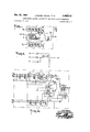
- FIGURE 1 is an explanatory block diagram of functions of a high speed digital ty-pe arithmetic unit in accordance with the present invention.
- FIGURE 2 is a schematic diagram of a logic circuit thereof.
- FIGURE 3 is a schematic diagram of a modification of said logic circuit.
- FIGURE 4 is an equivalent circuit of an and gate used in the logic circuit.
- the most important point of the unit of the present invention lies in the decimal carry judge logic circuit whose object is 1 digit of both of the summand and the addend registers, said 1 digit consisting of 4 bits.
- both of the summand and the addend registers are represented by the symbols of W and X respectively, and only each least significant digit is shown.
- the least significant digit (4 bits) respectively is constituted of four memory units which are so arranged from the upper digit to the lower digit as W W W W and X X X X Since both registers W and X numerical value information serially, they have the function of sequentially rightward shifting due to shift-signal S. Both registers W and X are further connected in order to memory units of upper digits W and X Both register outputs W and X of the summand and the addend registers are fed into a full adder which is provided with a carry memory circuit C and a sum output A is derived from the output thereof.
- a mere shift signal SK without carry and a shift signal SK having a carry and being accompanied with an addition of decimal value 6 are selectively fed into the summand register W.
- a direct shift signal is fed into the addend register X.
- t t t and t represent bit time signals.
- the addend register X herein used is a normal shift register having a function of rightward shift due to the shift signal S, and the application equations regarding its constitutional memory units X X X and X are as follows.
- the memory units W W W and W are to be controlled perform only the rightward shift (necessary in all cases of t of the combinations corresponding to NC shown in Table 1 and the cases of 1 t and t and application and logical equations at this time are as follows.
- Equations 8-11 and 1215 should be combined being accompanied with the conditions of respectively corresponding instruction signals, and application and logical equations of each memory unit are conclusively obtained as follows:
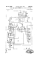
- FIGURE 2 shows a full logic circuit diagram in accordance with present invention in which an R-S fiipfi0p circuit is used in each of the memory units and respectively corresponding input equations are figured.
- the symbols in the drawing are same as those of FIGURE 1, and the explanation of the circuit is omitted.
- an equivalent and gate circuit is illustrated in FIGURE 4 to show the generation of SK and SK signals.
- the presence or the absence of a carry is judged by the decimal carry judge logic circuit CD, but in a modification of the embodiment of the present invention it is possible to make a correct judgment at the bit time t which is later by one than said 2 More specifically, the presence or the absence of a decimal carry to an upper place digit can be judged in accordance with the states of respective upper place three bits of the summand and the addend at the bit time t (the contents of six memory units W W W X3, X2 and X1).
- C is memorized in the carry memory circuit in the full adder AU, and represents the absence or the presence of a decimal carry from a lower place digit.
- the control in the case of fi of X X X X W W W and W is a mere rightward shift, and the input equations and logical equation of the output of each
- the embodiment of the present invention can perform the aforementioned operation by the use of memory units having properties expressed in Equations 1' and 5' to 14 and said signals, and can simply obtain a sum of two binary-coded decimal numbers without being accompanied with a time delay which otherwise is required for said compensation.
- FIGURE 3 shows a full logic circuit diagram of said modifications of the embodiment of the present invention in which the previously explained R-S flip flop circuit is used in each of the memory units and corresponding input equation is attained.
- the symbols in the drawing are same as those of FIGURE 1.
- An accompanying feature of the adder in accordance with the present invention is that by the utilization of the circuit function of the rightward shifting having a decimal value 6 being simultaneously added due to said signal SK it can be effectively combined and used as a complement unit of binary-coded decimal number.
- Equation 25 has the following meaning,
- a complement of a digit value a with respect to 9 is equal to a number obtained by adding 0110 (decimal value 6) to the binary expression of a, that is a a a a and complementizing the sum thereof with respect to 15, that is by converting each bit value of said sum in such manner as 1 to O and 0 to 1.
- the adder in accordance with the present invention has a large advantage that it can be effectively used to produce a complement unit of 9 with respect to the contents of the summand register when the following instruction is specially applied.
- circuit device in accordance with the present invention can be utilized as a subtracter when said function of a complement unit is added to said binary-coded decimal number adder.
- a high speed serial digital arithmetic computer with radix correction comprising at least two registers each having a plurality of memory elements for registering first and second operands represented by binary coded decimal numbers, a judging circuit interconnected with said registers and responsive to said stored binary codes to produce a first signal if the computation will involve the next upper decimal digit and a second signal if the computation will not involve the next upper decimal digit, means supplying one of said judging signals to one of said registers, said first judging signal applying a radix correction to said one register, a full adder, and means for feeding the information in said registers after the application of said judging signal to said full adder to produce a sum of the binary coded decimal numbers in said registers.
- a high speed serial digital arithmetic computer with radix correction including means to shift the binary coded decimals in said registers by one bit, and then applying one of said judging signals, said first judging signal omitting the least significant bit of said radix correction, said judging signal being determined by the three last significant bits in said registers following said shift.
- a high speed serial digital arithmetic computer with radix correction including means for producing said judging signal to apply a radix correction to one of said registers, whereupon information in the last said register may be inverted to produce the complement of the binary coded information stored therein.
Description
Dec. 23, 1969 ATSUSHI ASADA ET AL v 3,4s,01s
HIGH SPEED DIGi TAL ARITHMETIC UNIT WITH RADIX CORRECTION Filed May L7, 19% z Sheets-Sheet 2 n In x Ix INVENTOR6 3 AZswVsAzA nited States Patent 3,486,015 HIGH SPEED DIGITAL ARITHMETIC UNIT WITH RADIX CORRECTION Atsushi Asada and Isamn Washizuka, Osaka-shi, Japan, assignors to Hayakawa Denki Kogyo Kabushiki Kaisha, Osaka, Japan, a company of Japan Filed May 17, 1966, Ser. No. 550,758 Claims priority, application Japan, May 24, 1965, 40/30,725, i0/30,726 Int. Cl. G061? 7/385; H03k 19/00 US. C. 235170 3 Claims ABSTRACT OF THE DISCLOSURE A high speed digital type arithmetic computer wherein binary coded information is fed into registers, the information in said registers is then judged to determine whether a radix correction should be applied whereup the information is then fed to a full adder. The computer further includes means for shifting the coded information in said registers to effect radix correction by omitting the least significant digit and means for introducing the radix correction and producing a complement of the corrected number before said addition.
The present invention relates to a high speed digital type arithmetic unit, especially to a serial arithmetic unit having no time delay. Although the present invention is applicable not only to binary-coded decimal code, but also to other codes, for the convenience of explanation the following description will be directed to the case of binary-coded decimal code.
In the case of electronic serial arithmetic unit of a type in which numeral value information is indicated in binary-coded decimal number, when two numeral values are added by normal methods a sum thereof is produced at the output of an adder being accompanied with a time delay of 2 to 3 bit times. More specifically, as can be seen from the truth table of binary-coded decimal codes (8421 codes), the codes corresponding to decimal numbers from 0 to 9 are of same form as that of the binary notation, but when it comes to a code corresponding to decimal 10 a carry is made to the next upper digit, and it returns back to "0 again. On the other hand, in the case of binary notation, a carry is made at decimal 8, a next carry is made at decimal 16, and therefore in order to make a carry at binary value 1010 which corresponds to decimal 10 and to reset the code back to O at the same time it will do just to treat the binary value 1010 as the binary value 10000.
For the above mentioned purpose, it is necesary to add an operation so that binary value 0110 which is the diflerence betwen the binary values 10000 and 1010, that is decimal value 6, to numeral values of decimal 10 and above.
At the time of the above mentioned supplementing operation, it is necessary to judge by some means whether or not the numeral value of each digit of the addition output exceeds decimal value 9, and to add decimal value 6 only to the digit which exceeds decimal value 9. Therefore, time is required for said supplementing operation, and it results in a time delay.
On the other hand, in a serial type arithmetic unit, a delay as much as even one bit time is not allowable, and therefore the present arithmetic units various methods in order to compensate for said time delay and to maintain timing constant. However, said conventional compensating methods are complicated, and there is such a disadvantage that various linked problems are met in taking the timing of a series of control system including said compensation of the time delay.
"ice
Accordingly, an object of the present invention is to provide a novel high speed digital type arithmetic unit of serial operation type not having the disadvantages discussed above.
Another object is to provide a novel high speed digital type arithmetic unit of serial operation type in which a presence or an absence of a carry is judged from the memory contents of a first operand register and a second operand register, and while an operation is being performed a compensation of a difference due to the different kinds of codes of said registers and an operation device is simultaneously done.
Another object of the present invention is to provide a novel high speed digital ty-pe arithmetic unit of serial type in which a circuit which performs said operation together with said simultaneous compensation is simplified.
A further object of the present invention is to provide a novel high speed digital type arithmetic unit of serial type in which said means of supplementing by decimal value 6 is simple but certain.
A still further object of the present invention is to provide a novel high speed digital type arithmetic unit of serial type in which the registered numerical value of binary-coded decimal code is complementized in a simple manner.
In accordance with the present invention, a decimal carry judge logic circuit is provided for making a judgement of a presence or an absence of a carry in accordance with the memory contents of summand and addend registers. This is so arranged that if the judgement by said circuit indicates that a carry is not necessary a mere shift signal is applied to one of said registers so that an addition is done without a carry, and if said judgement indicates that a carry is necesary a shift signal which is accompanied with an addition of binary value 0110 (decimal value 6) is selectively applied to one of said registers, and thereby an addition with a carry is performed.
In accordance with another embodiment of the present invention, it is so arranged in order to obtain same efifect as the addition of the decimal value 6 the memory contents of said summand and addend registers are shifted by one bit, then a judgment of a presence or an absence of a carry is made, and in the case of a presence of a carry, a shift signal accompanied by the addition of binary value 011 is selectively applied to one of said registers. First shifting the numeral value information by one bit and subsequent addition of 011 attain same efiect as that of an addition of 0110 without a shift. Thus, the constitution of the unit is simplified in accordance with the present invention.
The present invention will be more clearly understood from the explanation hereinafter made referring to the drawings; wherein FIGURE 1 is an explanatory block diagram of functions of a high speed digital ty-pe arithmetic unit in accordance with the present invention.
FIGURE 2 is a schematic diagram of a logic circuit thereof.
FIGURE 3 is a schematic diagram of a modification of said logic circuit.
FIGURE 4 is an equivalent circuit of an and gate used in the logic circuit.
Referring to FIGURE 1, the most important point of the unit of the present invention lies in the decimal carry judge logic circuit whose object is 1 digit of both of the summand and the addend registers, said 1 digit consisting of 4 bits. In the drawing, both of the summand and the addend registers are represented by the symbols of W and X respectively, and only each least significant digit is shown.
The least significant digit (4 bits) respectively is constituted of four memory units which are so arranged from the upper digit to the lower digit as W W W W and X X X X Since both registers W and X numerical value information serially, they have the function of sequentially rightward shifting due to shift-signal S. Both registers W and X are further connected in order to memory units of upper digits W and X Both register outputs W and X of the summand and the addend registers are fed into a full adder which is provided with a carry memory circuit C and a sum output A is derived from the output thereof. From the output terminal of said decimal carry judge logic circuit, a mere shift signal SK without carry and a shift signal SK having a carry and being accompanied with an addition of decimal value 6 (binary value 0110) are selectively fed into the summand register W. A direct shift signal is fed into the addend register X. In the drawing, t t t and t represent bit time signals.
The addend register X herein used is a normal shift register having a function of rightward shift due to the shift signal S, and the application equations regarding its constitutional memory units X X X and X are as follows.
The logic equation of the output of said register is as follows.
X =SX (5 Now, there are bit time signals t t t and L; as the signals for determining the timing of bits of said arithmetic unit, and are so synchronized that at respective bit times the lowest bit (fourth place bit), the third place bit, the second place bit and the highest bit (first place bit) respectively appear a the least significant memory unit of each digit.
When the above mentioned synchronization is made, corresponding digits of the summand and the addend, four bits from the upper place respectively, are memorized in each of the memory units W W W W and X X X X at I at each digit time.
On the other hand, when the carry memory circuit C in the full adder AU is made with the. above mentioned timing to memorize a decimal carry from the lower digit thereof, the combination of the states which nine memory units, W W W W X X X X and C can take at this time and the presence and the absence of carry with respect to said combination are as shown in Table 1 In the above table, C represents a presence of a carry, and NC represents an absence of a carry.
For example, the expression of a summand and an addend (X X X X :0011 shows the case of 5+3 in which there is no carry from the lower place, the. answer is 8, and it is not accompanied with a carry (there is marked NC in the above table.) On the other hand, the expression of (W W W W ,C )=1001,l and xpr x x :1000
indicates (9+8) with a carry, and the answer is 8 being accompanied with a carry to the next digit. The latter case is marked C in the above table.
Considering the addition of binary-coded decimal numbers, digit values w and x of a summand and an addend, carry 0 from the lower place, carry 0' to the upper place, and digit value a of a sum are interrelated as follows since each digit value is represented by a binary number, when a binary sum is represented by F (W, x, c)
a=F (w, x, c) in case w+x+c9 (that is c' =0) and a=F (w, x, 0) +6 in case w-l-x-l-cZlO (that is c"=l) For an example of the former, if w=5, 10:3 and c=0 'w 0101 a: 0011 c 0 F('w,:v,c) 1000=8 0 =0 No-carry As an example. of the latter, if w'=9, x=8 and 0:1
w 1001 :v 1000 c 1 F(w,:c,c) 10010 0110 0 =1 There is a carry If the circuit is so constituted that the presence or the absence of a carry to the upper place digit regarding such states as shown in Table 1 at the bit time t is judged utilizing the relation of above Equation 6, in the case of the presence of a carry (it means all of the cases for which C is marked in the above table) not only the summand digits W W W and W are shifted rightwardly but also decimal value 6 is simultaneously added during the shift, and said circuit is operated by a e udge signal of the presence of a carry (represented by TABLE 1 X4XXX W4WsW2W1 3 2 1 1 o o o o o o o o o o 0 c o o o o o o o (3 NC 1 o 0 o o o o o o o No 0 o o o 0 o o o o No No 1 o o o o o o o 0 NC NC 0 o o o o o o o NC NC NC 1 o o o o o o 0 NC NC NC 0 o o 0 o o o NC NC NC NC 1 o o o 0 o 0 NC NC NC NC 0 o o o o o NC NC No NC NC 1 o o o o o N0 NC NC NC NC 0 o o 0 0 NC NC NC No N0 N0 1 o o o 0 N0 NC NC NC NC No 0 o 0 O NC No No NC NC NC NC 1 o o 0 NC NC NC NC NC NC NC 0 o 0 NC NC NC NC NC NC NC NC 1 o o NC NC NC NC NC NC NC NC 0 o NC NC NC NC NC No NC NC NC 1 o No NC NC NO NC NC NC N0 N0 0 NC NC NC NC NC NC NC NC NC NC 5 the mark SK in FIGURE 1), thereby a binary output of a sum as it is and a carry signal for a carry from the uppermost place bit thereof to a higher digit are automatically obtained as an output (marked A in FIGURE 1) of the full adder AU.
With respect to a judgment of an absence of a carry (it means all cases marked NC in Table 1), when a mere rightward shift is indicated (by signal marked SK in FIGURE 1) the output A of the full adder AU automatically represents a sum thereof. It is apparent from the relation shown in the Equation 6 that it is not necessary to take into consideration regarding a carry to an upper digit.
A serial analysis of the aforementioned examples are shown in Tables 2(a) and 2(b) below.
(a) The case of no-carry to the upper digit (that is the case that a control is made by the signal SK).
TABLE 2(a) wiwnvzwi WE=W1 XiXaXgXi XE=X1 C A case that a control is made by the signal SK).
TABLE 2(b) W4WaWzW1 WE=W1 X4XaXzX1 XE=X1 l C A In the above table, the output A of the full adder AU is indicating 1000 with a carry, that means decimal value l0+8=18. (*3) represents a carry from lower place digit, (*4) represents a state obtained by adding 0110 (decimal value 6) to 1001, and shifting 1111 rightwardly, and 5) represents the presence of a carry to an upper place digit.
As can be seen from the above examples of calculation made in accordance with the present invention, by making selective control of either one that W W W and W are merely shifted rightwardly from the state of nine memory units of W W W W X X X X and C or that they are shifted rightwardly simultaneously having decimal value 6 being added thereto, it is made possible using normal full adder to automatically obtain as an output therefrom a sum of two binary-coded decimal numbers and a carry to an upper digit.
A logical equation for representing all of the combinations with respect to the mark C of Table 1 is shown below. This means that an instruction signal SK for shifting rightwardly having decimal value 6 being added is obtained, and this signal should be generated at t only.
All of the controls to be performed by said signal SK, that is all of the states of controls for shifting rightwardly having decimal value 6 added simultaneously, are shown in Table 3.
TABLE 3 State at 11 State at 2 Output at 1 WiWiWgW VJVVEWQVl V E 0000 011 0 0001 011 1 0010 0 0011 100 1 0100 101 0 0101 101 1 0110 0 0111 110 1 1000 111 0 1001 111 1 Application and logical equations of the output of each memory unit which satisfy various states as shown in Table 3 are as follow:
On the other hand, under the instruction signal SK, instead of the instruction signal SK determined by the Equation 7, the memory units W W W and W are to be controlled perform only the rightward shift (necessary in all cases of t of the combinations corresponding to NC shown in Table 1 and the cases of 1 t and t and application and logical equations at this time are as follows.
The Equations 8-11 and 1215 should be combined being accompanied with the conditions of respectively corresponding instruction signals, and application and logical equations of each memory unit are conclusively obtained as follows:
On the other hand, since the memory unit W always receives a control only when the contents are rightwardly shifted from an upper place digit, it follows that the following application equation.
It is to be noted that, the logical equation of normal full adder which is used in the present invention and an application equation of a carry memory unit included therein are as follows.
E E-i- E E (2 In accordance with the present invention, by the use of memory units having properties indicated by the above explained Equations l4, 5, 7, and 1621 and respective signals it has become possible to accomplish the operations above explained and to simply obtain a sum of two binary-coded decimal numbers without being accompanied by a time delay which is otherwise required for compensation.
As an example of embodiment of the present invention, FIGURE 2 shows a full logic circuit diagram in accordance with present invention in which an R-S fiipfi0p circuit is used in each of the memory units and respectively corresponding input equations are figured. The symbols in the drawing are same as those of FIGURE 1, and the explanation of the circuit is omitted. For clarity, an equivalent and gate circuit is illustrated in FIGURE 4 to show the generation of SK and SK signals.
At the bit time t in the previously explained example of embodiment of the present invention the presence or the absence of a carry is judged by the decimal carry judge logic circuit CD, but in a modification of the embodiment of the present invention it is possible to make a correct judgment at the bit time t which is later by one than said 2 More specifically, the presence or the absence of a decimal carry to an upper place digit can be judged in accordance with the states of respective upper place three bits of the summand and the addend at the bit time t (the contents of six memory units W W W X3, X2 and X1).
When each of the summand and the addend is shifted rightwardly, as to the carry the contents obtained in accordance with the logic of the normal binary full adder are applied, and the classification of carry C and nocarry NC corresponding to the combinations of the time are made to correspond, the following Table 4 can be obtained without encountering any discrepancy.
TABLE 4 XaXzXi C C C C C C C C NC C C C C NC C C 0 NC NC C C 0 NC NC C O NC NC NC 0 O NC NC NC 0 NC NC NC NC C NC NC NC NC NC NC NC NC NC In the above, C is memorized in the carry memory circuit in the full adder AU, and represents the absence or the presence of a decimal carry from a lower place digit.
For example, the state is as follows in case at the time t the summand (W W W W C )=O1O1, 0 and the addend (X X X X )=0011.
W4W W2W1 X4X3X2X1 C In this case, there is marked NC in the table.
On the other hand, the following represents the case that the summand (W W W W C )=1001, 1 and the addend (X X X X =1000.
I W WaWzW X4X3X2X1 I C it a -I 1001 1000 l 12--...-" 100 100 1 In this case, there is marked 0 in the table.
A logical equation representative of all of the combinations corresponding to the carry mark C in the Table 4 can be attained as follows.
TABLE 5(a) W4W W2Wi WE X4X XZX1 XE=X1 C A 0101 0011 1 0 O 010 001 1 l 0 201 1 O0 0 1 In the above table, A is a full adder output of three inputs of W X and C. C is a memory circuit of carry in the full adder of three inputs of W X and C. The logic of both is conventional and explanation is omitted. (*1) indicates that W W in the case of SK, and (*2) indicates a mere rightward shift in the case of SK.
(b) The case of a carry to an upper place digit (the case of control by the signal SK).
TABLE 503) As the output in the above table shows 1000 with a carry, is the decimal value 18.
In the above case, SK is indicated at t therefore the number to be added is not 0110 but is 011, thus 01 1 is added to 100, and the output W and next state shifted rightwardly are determined with respect to the resultant 111. (*3) represents W I (in this case only W W and (*4) represents the state 11, that is 111 is shifted rightwardly.
Following the manner of the above Table 5 (b), the controls to be performed by the signal SK in connection with the combinations corresponding to C of Table 4 are Application equations and the logical equation of the output which satisfy various states shown in Table 6 are as follows.
The control in the case of fi of X X X X W W W and W is a mere rightward shift, and the input equations and logical equation of the output of each The embodiment of the present invention can perform the aforementioned operation by the use of memory units having properties expressed in Equations 1' and 5' to 14 and said signals, and can simply obtain a sum of two binary-coded decimal numbers without being accompanied with a time delay which otherwise is required for said compensation.
FIGURE 3 shows a full logic circuit diagram of said modifications of the embodiment of the present invention in which the previously explained R-S flip flop circuit is used in each of the memory units and corresponding input equation is attained. The symbols in the drawing are same as those of FIGURE 1.
An accompanying feature of the adder in accordance with the present invention is that by the utilization of the circuit function of the rightward shifting having a decimal value 6 being simultaneously added due to said signal SK it can be effectively combined and used as a complement unit of binary-coded decimal number.
Suppose a complement of a certain number with respect to 9 is to be obtained. This requires the production of the complement of each of decimal digit value with respect to 9, and the following relation exists between the original digit value a and its complement (a) with respect to 9.
(a)=9-a (decimal expression) (23) When the digit value a is indicated in a binary code, if a complement of each bit is taken (that is to convert 1 to and 0 to 1), this means to complementize 1111, that is the decimal value 15, then the following relation exists between the original binary numbers a a a and a and the complements E 5 5 and H (5 5 5 5 (1 l1 1 (a a a a (binary expression) The above two Equations 23 and 24 are combined in such relation as a (decimal expression)=a a a a (binary expression), and (E) to be obtained can be expressed as follows.
= a6 (decimal expression) =1111 (a a a a +01 10) (binary expression) When the Equations 25 and 24 are compared, it can be clearly seen that the Equation 25 has the following meaning,
A complement of a digit value a with respect to 9 is equal to a number obtained by adding 0110 (decimal value 6) to the binary expression of a, that is a a a a and complementizing the sum thereof with respect to 15, that is by converting each bit value of said sum in such manner as 1 to O and 0 to 1.
The control to add the decimal value 6 is possible by always making K=1 as was previously explained, and the conversion from 1 to 0 and from 0 to 1 can be simply accomplished by making it to pass through a stage of inversion. Thus, the adder in accordance with the present invention has a large advantage that it can be effectively used to produce a complement unit of 9 with respect to the contents of the summand register when the following instruction is specially applied.
Complementized output=W Further, it is apparent that the circuit device in accordance with the present invention can be utilized as a subtracter when said function of a complement unit is added to said binary-coded decimal number adder.
What is claimed is:
1. A high speed serial digital arithmetic computer with radix correction comprising at least two registers each having a plurality of memory elements for registering first and second operands represented by binary coded decimal numbers, a judging circuit interconnected with said registers and responsive to said stored binary codes to produce a first signal if the computation will involve the next upper decimal digit and a second signal if the computation will not involve the next upper decimal digit, means supplying one of said judging signals to one of said registers, said first judging signal applying a radix correction to said one register, a full adder, and means for feeding the information in said registers after the application of said judging signal to said full adder to produce a sum of the binary coded decimal numbers in said registers.
2. A high speed serial digital arithmetic computer with radix correction according to claim 1 including means to shift the binary coded decimals in said registers by one bit, and then applying one of said judging signals, said first judging signal omitting the least significant bit of said radix correction, said judging signal being determined by the three last significant bits in said registers following said shift.
3. A high speed serial digital arithmetic computer with radix correction according to claim 1 including means for producing said judging signal to apply a radix correction to one of said registers, whereupon information in the last said register may be inverted to produce the complement of the binary coded information stored therein.
References Cited UNITED STATES PATENTS 3,089,644 5/1963 Wensley 235- X 3,083,910 4/1963 Berkin 235170 X 3,112,396 11/1963 Heywood 235176 X 2,943,790 7/1960 Berezin et al. 235170 2,923,474 2/1960 Blankenbaker 235170 OTHER REFERENCES R. Townsend: Serial Digital Adders For a Variable Radix of Notation, Electronic Engineering, October 1953, pp. 410-416.
R. K. Richards Arithmetic Operations in Digital Computers, 1955, page 179.
EUGENE G. BOT Z, Primary Examiner DAVID H. MALZAHN, Assistant Examiner US. Cl. X.R. 235-176
Applications Claiming Priority (2)
| Application Number | Priority Date | Filing Date | Title |
|---|---|---|---|
| JP3072565 | 1965-05-24 | ||
| JP3072665 | 1965-05-24 |
Publications (1)
| Publication Number | Publication Date |
|---|---|
| US3486015A true US3486015A (en) | 1969-12-23 |
Family
ID=26369127
Family Applications (1)
| Application Number | Title | Priority Date | Filing Date |
|---|---|---|---|
| US550758A Expired - Lifetime US3486015A (en) | 1965-05-24 | 1966-05-17 | High speed digital arithmetic unit with radix correction |
Country Status (4)
| Country | Link |
|---|---|
| US (1) | US3486015A (en) |
| DE (1) | DE1524131B1 (en) |
| GB (1) | GB1150424A (en) |
| NL (1) | NL6607052A (en) |
Cited By (1)
| Publication number | Priority date | Publication date | Assignee | Title |
|---|---|---|---|---|
| US4172288A (en) * | 1976-03-08 | 1979-10-23 | Motorola, Inc. | Binary or BCD adder with precorrected result |
Citations (5)
| Publication number | Priority date | Publication date | Assignee | Title |
|---|---|---|---|---|
| US2923474A (en) * | 1953-09-02 | 1960-02-02 | Hughes Aircraft Co | Multiple input binary-coded decimal adders and subtracters |
| US2943790A (en) * | 1956-01-10 | 1960-07-05 | Curtiss Wright Corp | Arithmetic device |
| US3083910A (en) * | 1955-08-01 | 1963-04-02 | Ibm | Serial adder and subtracter |
| US3089644A (en) * | 1959-03-24 | 1963-05-14 | Developments Ltd Comp | Electronic calculating apparatus |
| US3112396A (en) * | 1957-05-03 | 1963-11-26 | Ibm | Arithmetic circuitry |
Family Cites Families (3)
| Publication number | Priority date | Publication date | Assignee | Title |
|---|---|---|---|---|
| DE1121383B (en) * | 1959-09-11 | 1962-01-04 | Elektronische Rechenmasch Ind | Binary arithmetic unit for additions and subtractions of two encrypted decimal numbers |
| DE1126166B (en) * | 1959-10-14 | 1962-03-22 | Ibm | Serial number calculator |
| DE1140380B (en) * | 1960-08-16 | 1962-11-29 | Telefunken Patent | Arrangement for decimal addition in a binary parallel arithmetic unit |
-
1966
- 1966-05-17 US US550758A patent/US3486015A/en not_active Expired - Lifetime
- 1966-05-23 DE DE1966H0059480 patent/DE1524131B1/en active Pending
- 1966-05-23 NL NL6607052A patent/NL6607052A/xx unknown
- 1966-05-24 GB GB23095/66A patent/GB1150424A/en not_active Expired
Patent Citations (5)
| Publication number | Priority date | Publication date | Assignee | Title |
|---|---|---|---|---|
| US2923474A (en) * | 1953-09-02 | 1960-02-02 | Hughes Aircraft Co | Multiple input binary-coded decimal adders and subtracters |
| US3083910A (en) * | 1955-08-01 | 1963-04-02 | Ibm | Serial adder and subtracter |
| US2943790A (en) * | 1956-01-10 | 1960-07-05 | Curtiss Wright Corp | Arithmetic device |
| US3112396A (en) * | 1957-05-03 | 1963-11-26 | Ibm | Arithmetic circuitry |
| US3089644A (en) * | 1959-03-24 | 1963-05-14 | Developments Ltd Comp | Electronic calculating apparatus |
Cited By (1)
| Publication number | Priority date | Publication date | Assignee | Title |
|---|---|---|---|---|
| US4172288A (en) * | 1976-03-08 | 1979-10-23 | Motorola, Inc. | Binary or BCD adder with precorrected result |
Also Published As
| Publication number | Publication date |
|---|---|
| DE1524131B1 (en) | 1971-04-01 |
| NL6607052A (en) | 1966-11-25 |
| GB1150424A (en) | 1969-04-30 |
Similar Documents
| Publication | Publication Date | Title |
|---|---|---|
| US3100835A (en) | Selecting adder | |
| CN100440136C (en) | Arithmetic unit | |
| US3795880A (en) | Partial product array multiplier | |
| US3711693A (en) | Modular bcd and binary arithmetic and logical system | |
| US4878192A (en) | Arithmetic processor and divider using redundant signed digit arithmetic | |
| US4805131A (en) | BCD adder circuit | |
| US3210737A (en) | Electronic data processing | |
| US3621218A (en) | High-speed divider utilizing carry save additions | |
| US3626167A (en) | Scaling and number base converting method and apparatus | |
| JPS584440A (en) | Arithmetic logic unit | |
| US4866655A (en) | Arithmetic processor and divider using redundant signed digit | |
| US3486015A (en) | High speed digital arithmetic unit with radix correction | |
| US5365471A (en) | Divider for performing signed division using a redundant signed digit | |
| EP0044450B1 (en) | Digital adder circuit | |
| JPH0346024A (en) | Floating point computing element | |
| US3937941A (en) | Method and apparatus for packed BCD sign arithmetic employing a two's complement binary adder | |
| US3198939A (en) | High speed binary adder-subtractor with carry ripple | |
| US4873660A (en) | Arithmetic processor using redundant signed digit arithmetic | |
| US3112396A (en) | Arithmetic circuitry | |
| US3564225A (en) | Serial binary coded decimal converter | |
| US3786490A (en) | Reversible 2{40 s complement to sign-magnitude converter | |
| US5280440A (en) | Parallel adding circuit using 3×3 matrix of ± quinary number representation | |
| US5206825A (en) | Arithmetic processor using signed-digit representation of external operands | |
| US5153847A (en) | Arithmetic processor using signed digit representation of internal operands | |
| US3462589A (en) | Parallel digital arithmetic unit utilizing a signed-digit format |