US3290515A - Controlled pulse progression circuits with complementary transistors - Google Patents
Controlled pulse progression circuits with complementary transistors Download PDFInfo
- Publication number
- US3290515A US3290515A US283940A US28394063A US3290515A US 3290515 A US3290515 A US 3290515A US 283940 A US283940 A US 283940A US 28394063 A US28394063 A US 28394063A US 3290515 A US3290515 A US 3290515A
- Authority
- US
- United States
- Prior art keywords
- transistor
- pulse
- conductive
- circuit
- resistor
- Prior art date
- Legal status (The legal status is an assumption and is not a legal conclusion. Google has not performed a legal analysis and makes no representation as to the accuracy of the status listed.)
- Expired - Lifetime
Links
- 230000000295 complement effect Effects 0.000 title description 6
- 230000015556 catabolic process Effects 0.000 claims description 106
- 230000008878 coupling Effects 0.000 claims description 62
- 238000010168 coupling process Methods 0.000 claims description 62
- 238000005859 coupling reaction Methods 0.000 claims description 62
- 230000004044 response Effects 0.000 claims description 19
- 230000000977 initiatory effect Effects 0.000 claims description 5
- 239000003990 capacitor Substances 0.000 description 83
- 241001657674 Neon Species 0.000 description 56
- 229910052754 neon Inorganic materials 0.000 description 54
- GKAOGPIIYCISHV-UHFFFAOYSA-N neon atom Chemical compound [Ne] GKAOGPIIYCISHV-UHFFFAOYSA-N 0.000 description 52
- 238000010586 diagram Methods 0.000 description 14
- 230000008859 change Effects 0.000 description 9
- 230000004048 modification Effects 0.000 description 7
- 238000012986 modification Methods 0.000 description 7
- 230000009471 action Effects 0.000 description 5
- 230000008901 benefit Effects 0.000 description 5
- XUIMIQQOPSSXEZ-UHFFFAOYSA-N Silicon Chemical compound [Si] XUIMIQQOPSSXEZ-UHFFFAOYSA-N 0.000 description 4
- 238000010891 electric arc Methods 0.000 description 4
- 229910052710 silicon Inorganic materials 0.000 description 4
- 239000010703 silicon Substances 0.000 description 4
- 239000007787 solid Substances 0.000 description 4
- 230000005540 biological transmission Effects 0.000 description 3
- 238000001914 filtration Methods 0.000 description 3
- 238000004804 winding Methods 0.000 description 3
- 230000000694 effects Effects 0.000 description 2
- WABPQHHGFIMREM-RKEGKUSMSA-N lead-214 Chemical compound [214Pb] WABPQHHGFIMREM-RKEGKUSMSA-N 0.000 description 2
- 150000002806 neon Chemical class 0.000 description 2
- 238000009877 rendering Methods 0.000 description 2
- 235000006026 Durio Nutrition 0.000 description 1
- 241000934928 Durio Species 0.000 description 1
- 238000010276 construction Methods 0.000 description 1
- 230000001419 dependent effect Effects 0.000 description 1
- 230000001747 exhibiting effect Effects 0.000 description 1
- 229920000136 polysorbate Polymers 0.000 description 1
- 230000001960 triggered effect Effects 0.000 description 1
Images


Classifications
-
- H—ELECTRICITY
- H03—ELECTRONIC CIRCUITRY
- H03K—PULSE TECHNIQUE
- H03K23/00—Pulse counters comprising counting chains; Frequency dividers comprising counting chains
- H03K23/82—Pulse counters comprising counting chains; Frequency dividers comprising counting chains using gas-filled tubes
-
- H—ELECTRICITY
- H03—ELECTRONIC CIRCUITRY
- H03K—PULSE TECHNIQUE
- H03K23/00—Pulse counters comprising counting chains; Frequency dividers comprising counting chains
- H03K23/002—Pulse counters comprising counting chains; Frequency dividers comprising counting chains using semiconductor devices
Definitions
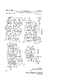
- FIG. 8a FIG 8b INVENTOR.
- Samud A Procter BY @7714 990M M W /ac Afior-neqs Dec. 6, 1966 s.
- A. PROCTER CONTROLLED PULSE PROGRESSION CIRCUITS WITH COMPLEMENTARY TRANS S TORS 7 Sheets-Sheet 5 Filed May 28, 1963 INVENTOR. Samuel A. Pmder A Torneqs Dec. 6, 1966 s.
- PROCTER CONTROLLED PULSE PROGRESSION CIR 3,2 90,515 GUITS WITH COMPLEMENTARY TRANS I STORS '7 Sheets-Sheet 6 Filed May 28, 1963 Dec, O, 1966 s PROCTER 3,290,515
- One object of the present invention is to provide new and improved circuits comprising a plurality of electronic devices which are rendered successively conductive by successive input pulses.
- a further object is to provide new and improved circuits of the foregoing character which utilize electronic breakdown devices, such as neon or other gaseous discharge lamps, are discharge tubes such as T-hyratro'ns, transistor latching circuits, or various types of solidstate devices, such as Shockley diodes, for example.
- electronic breakdown devices such as neon or other gaseous discharge lamps
- discharge tubes such as T-hyratro'ns, transistor latching circuits, or various types of solidstate devices, such as Shockley diodes, for example.
- Another object is to provide new and improved pulse progression circuits utilizing a plurality of electronic breakdown devices connected in sequence or cascade by a plurality of coupling devices, which may include capacitors, transformers, or transistors, for example.
- a further object is to provide new and improved pulse progression circuits of the foregoing character having means whereby only one of the breakdown devices can be conductive at any one time.
- Another object is to provide new and improved pulse progresson circuits having a plurality of electronic breakdown devices connected in sequence by a plurality of coupling devices, together with an impedance common to all of the breakdown devices, so that only one of the devices can be conductive at any one time, and means responsive to an input pulse for rendering the conductive device nonconductive, the coupling devices being effective to produce a transfer signal which initiates conduction in the next breakdown device in the sequence, in response to the stopping of conduction in the initially conductive device, so that successive input pulses cause the breakdown devices to be successively conductive.
- Another object is to provide a new and improved pulse progression circuit which may readily be arranged to provide a counter, operating with any number as the counting base, said counter generally having considerably fewer electronic components than other types of counters, such as flip-flop circuits utilizing transistors.
- a further object is to provide new and improved counter or other pulse progression circuits having a sequence of stages which become conductive successively, only one of the stages being conductive at one time, so that the current consumption of the counter is greatly reduced, particularly when compared with counters using flip-flops.
- Another object is to provide a new and improved transistor latching or switching circuit for use in counters, pulse progression circuits, or other electronic devices.
- a further object is to provide variations of the tran- 3 ,290,515 Patented Dec. 6, 1966 sistor latching circuit for use as trigger circuits and pulse generators.
- FIG. 1 is a schematic circuit diagram of a pulse progression circuit to be described as an illustrative embodiment of the present invention.
- FIG. 2 is a fragmentary circuit diagram showing a modified pulse progression circuit utilizing coupling transformers between the electronic breakdown devices.
- FIG. 3 is a circuit diagram of another modified pulse progression or counter circuit employing transistors in the coupling circuits between the electronic breakdown devices.
- FIG. 4 is a circuit diagram illustrating another pulse progression circuit utilizing grid controller arc discharge tubes as the electronic breakdown devices.
- FIG. 5 is a circuit diagram of another modified pulse progression circuit arranged to provide a device which counts events per unit time.
- FIG. 6 is a circuit diagram of another pulse progression circuit utilizing transistors in the coupling circuits between the electronic breakdown device's.
- FIGS. 7a, 7b, 8a, 8b, 9a, and'9b comprise oscillograms illustrating the wave form of various signals in the circuit of FIG. 6.
- FIG. 10 is a circuit diagram of another pulse progression circuit constructed in accordance with the present invention.
- FIGS. 10a and 10b are fragmentary circuit diagrams illustrating modifications of FIG. 10 utilizing different breakdown devices.
- FIG. 11 is a circuit diagram of another pulse progression circuit utilizing special transistor latching circuits as the breakdown devices.
- FIG. 11a comprises oscillograms showing the wave forms of input and output signals for the circuit of FIG. 11.
- FIG. 12a is a circuit diagram showing the transistor latching or switching circuit as employed in FIG. 11.
- FIG. 12] is a circuit diagram showing a modification of FIG. 12a to provide a trigger circuit.
- FIG. is a circuit diagram of another modification of FIG. 12a to provide a self-excited pulse generator.
- FIG. 1 illustrates a pulse progression circuit 10 which constitutes an illustrative embodiment of the present invention.
- the illustrated circuit 10 may be characterized as an elementary counter circuit.
- the pulse progression or counter circuit 10 comprises a plurality of electronic breakdown devices.
- illustrated circuit 10 utilizes three such breakdown devices which will be designated 12a, 12b, and 120 for convenient identification. However, it will be realized that any suitable number of break-down devices may be employed, according to the number which is to be employed as the counting base. Thus, the illustrated counter is adapted to count to the base 3.
- the illustrated electronic breakdown devices 12a-12c take the form of small neon glow discharge lamps, but various other types of electronic breakdown devices may be employed.
- the neon lamps may be replaced with other types of gaseous discharge lamps or tubes, are discharge lamps or tubes, or solid state devices such as Shockley diodes or controlled irectifiers.
- any such breakdown device should have the ability to change from a non-conductive state to a conductive state in response to a change in the voltage applied to the device, but without any need for a change in polarity, and the device should be able to maintain conduction at a voltage lower than the voltage required for breakdown or initiacircuit 24a in detail.
- neon or other gaseous discharge lamps have these characteristics.
- neon lamps are readily available and low in cost.
- neon lamps are well suited for use in the pulse progression circuit of FIG. 1.
- the neon lamps may be small in size and of the type commonly used for small pilot lamps.
- the neon lamps 12a-12c are adapted to be energized by a battery 14 or some other source of direct current.
- the negative terminal of the direct-current source 14 is grounded, while the positive terminal is connected to 'a positive supply lead 16.
- the energizing circuit for the neon lamps 12a-12c comprises a common resistor or impedance 18 which in this case is connected between ground and common lead 20 extending to one terminal of each of the neon lamps 12a-12c. Thus, any current which passes through any of the lamps must pass through the resistor 18.
- Load resistors 22a, 22b, and 220 are connected between the respective lamps 12a-12c and the positive lead 16.
- the common resistor 18 is made of such a high value of resistance that only one of the neon discharge lamps 12a-12c can be conductive at any one time. A minimum current is required to maintain the electron discharge in any of the neon lamps.
- the resistance value of the resistor 18 is made sufficiently great, with reference to the supply voltage, to limit the current through the resistor to a value substantially less than twice the minimum discharge current for each lamp, so that the discharge can be maintained in only one lamp at a time.
- the breakdown devices 12a-12c are connected in sequence or cascade by a series of coupling circuits 24a, 24b, and 240.
- each coupling circuit 24ac is connected between the corresponding breakdown device 12a-c and the next breakdown device in sequence.
- the coupling circuit 240 is connected between the breakdown device 120 and the breakdown device 12a so that the circuit forms a closed ring.
- the pulse progression device is provided with an input circuit 40 for momentarily interrupting conduction in all of the breakdown devices 12a-c in response to each input pulse.
- the input pulses are applied across input terminals 42 and 44.
- a coupling capacitor 46 is connected between the input terminal 42 and the common lead 20.
- the other input terminal 44 is grounded.
- the input pulses are positive in polarity.
- Each of the input pulses is great enough in magnitude to reduce the voltage across the conductive lamp to a value which is insufficient to maintain the discharge in the lamp.
- the coupling circuit 24a generates a transfer pulse which is supplied to the next lamp 12b in response to the stoppage of conduction in the first lamp 12a.
- the transfer pulses are produced primarily by the load resistors 22a-c and the capacitors 30a-c.
- the capacitor 30a is charged to a voltage corresponding to the voltage drop across the load resistor 12a.
- the input pulse renders the lamp 12a non-conductive
- the voltage across the capacitor 30a is applied to the second lamp 12b through the diode 24a and the resistor 36a, so as to increase the total voltage across the second lamp.
- conduction is initiated in the second lamp 12b at the end of the input pulse.
- the capacitor 30a discharges through the resistors 22a and 38a.
- the second capacitor 30b is charged through the load resistor 22b and the resistor 38b.
- the diodes 34a-c cause the lamps 12a-c to be energized in the correct sequence and not in the reverse sequence.
- a large output pulse is produced for every third input pulse.
- the pulse progression circuit 10 is adapted to count to three .repeatedly. If a higher count is desired, successive ring counters may be connected in cascade. Thus, any of the output terminals 28ac may be connected to the input terminal of another ring counter. Likewise, one of the output terminals of the second ring counter may be connected to the input terminal of a third ring counter, etc.
- FIG. 2 illustrates a modified pulse progression circuit 50 which is similar to the circuit 10 of FIG. 1 except that the circuit 50 employs modified coupling circuits 52a-c in place of the circuits 24a-c. All of the coupling circuits 52a-c are the same, so that only the coupling circuit 52b may be described in detail.
- the coupling circuit 52b comprises a pulse transformer 54b and a capacitor 56b.
- the transformer 54b is of the auto-transformer type, having a tap 58b and end terminals 60b and 62b.
- the tap 58b divides the transformer 54b into two portions, 64b and 66b.
- the primary portion 64b between the tap 58b and the end terminal 60b, has a relatively small number of turns, while the secondary portion 66b has a much larger number of turns.
- the load resistor 22b is connected to the end terminal 60b, while the tap 58b is connected to a lead 68b extending to one electrode of the neon lamp 12b.
- the load resistor 22b and the primary portion 64b of the transformer 54b are connected in series between the positive supply lead 16 and the neon lamp 12b.
- the capacitor 56b is connected between the other end terminal 52b and the lead 680 which extends to the next lamp 120.
- the secondary portion 66b of the transformer 54b is connected in series with the capacitor 56b to the next lamp 12c.
- the discharge current through the lamp also flows through the primary portion 64b of the transformer 54b.
- the interruption of the current through the primary winding 64b generates a high voltage pulse in the secondary winding 66b.
- This pulse is transmitted to the next lamp 120 and causes it to become conductive at the end of the input pulse. Because of the step-up effect of the transformer in each coupling circuit, the pulse progression circuit of FIG. 2 has improved reliability so that it is insensitive to variations in the characteristics of the neon lamps, the supply voltage, and the values of the various resistors and capacitors.
- FIG. 3 illustrates another modified pulse progression circuit 70 which is similar to the circuit 10 of FIG. 1, except that the circuit 70 comprises modified coupling circuits 72a-c utilizing amplifying devices 74a-c.
- the amplifying devices 74a-c take the form of transistors, but vacuum tubes or other amplifying devices may be employed. All of the coupling circuits 72a-c are the same, so that only the coupling device 72a need be described in detail.
- a load resistor 76a is connected between the positive supply lead 16 and the collector of the transistor 74a.
- the emitter of the transistor 74a is connected to a lead 78a which extends to one electrode of the neon lamp 12a.
- a coupling capacitor 80a is connected between the collector of the transistor 74a and the emitter of the transistor 74b for the next lamp 1217.
- An output terminal 82a may be connected to the collector of the transistor 74a.
- a filtering or bypass capacitor '86 is connected between the lead 84 and ground.
- the neon lamp 12a is conductive while the other lamps 12b and 12c are not conductive.
- the common resistor 18 prevents conduction in more than one lamp at any one time.
- the transistor 74a is arranged with its collector-emitter path in series with the lamp 12a. Thus, the transistor 74a is conductive when the lamp 12a is conductive.
- the drop across the transistor is quite small, usually less than one v-olt.
- the base, emitter, and collector of the transistor 74a are all at about the same potential.
- the base of the transistor 74a assumes a voltage which is substantially equal to the total voltage drop across the lamp 12a and the resistor 18, plus the small drop across the transistor.
- the voltage at the base of the transistor 74a may be about 62 volts with a power supply potential of 90 volts.
- the drop across the resistor 18 may be about 12 volts.
- the capacitor 86 is large enough to prevent any rapid changes in the voltages on the bases of the three transistors 74a-c. Thus, the base voltage remains at all times at about 62 volts.
- the positive input pulses are applied across the common resistor 18.
- the input pulses may have a magnitude of perhaps 20 volts, for example.
- the first pulse causes the lamp 12a to become non-conductive, so that all of the lamps are non-conductive momentarily.
- the interruption of the emitter current in the transistor 74a also causes interruption of the collector current, so that the voltage at the collector rises rapidly to the full 90 volts of the power supply.
- This pulse of voltage is applied by the capacitor 80a to the next lamp 12b, which thus is rendered conductive.
- the next input pulse transfers the conduction to the lamp 12c, etc., around the ring. It will be recognized that each transistor acts as a switch for its own lamp and as an amplifier or transfer device to trigger the next lamp in the sequence.
- FIG. 4 illustrates a modified pulse progression circuit 110 which employs breakdown devices 112a-c, illustrated as grid-controlled arc discharge tubes, such as thyratrons, for example. It will be realized, however, that other types of breakdown devices may be employed, such as controlled solid state rectifiers, for example.
- the energizing voltage for the thyratrons 112ac is applied between ground and a positive supply lead 116.
- a common resistor or impedance 118 is connected between ground and a lead 120 which is connected to the cathodes of all three thyratrons 112ac. It will be realized that any desired number of thyratrons may be employed, according to the number which is to be utilized as the counting base.
- the resistor 118 is sufficiently high in value to insure that only one of the thyratrons 112a-c will be conductive at a time.
- Load resistors 122a-c are connected between the positive supply lead 116 and the plates of the respective thyratrons 112a-c.
- positive input pulses are applied across the common resistor 118 by means of a capacitor 146 connected to an input terminal 142, the input terminal 144 being grounded.
- Output terminals 128a-c may be connected to the plates of the thyratrons 112a-c.
- Coupling circuits or devices 124a-c are provided between the successive thyratrons 112ac. All of the coupling circuits 124a-c may be the same, so that only the coupling circuit 124a need be described in detail.
- This circuit comprises a capacitor 150a connected between the plate of the thyratron 6 112a and the control grid or electrode of the thyratron 1121).
- a grid resistor 152a is connected between the grid of the thyratron 112 b and ground.
- the thyratron 112a is conductive, while the other thyratrons 11211 and 1120 are not conductive.
- the first positive input pulse at the cathode of the thyratron 112a reduces the voltage between the plate and cathode to such an extent that the thyratron 112a becomes non-conductive.
- the rapid rise in the positive voltage at the plate of the thyratron 112a produces a positive voltage pulse which is transmitted by the capacitor a to the control grid of the next thyratron 112k.
- the thyratron 112b becomes conductive.
- the next input pulse transfers the conduction to the thyratron 1120, and so forth around the ring.
- the two ring counters 162 and 164 are substantially the same so that only the ring counter 16-2 need be described in full detail.
- Direct current for energizing the circuit is derived from a battery or other source 166 having its negative terminal grounded.
- the positive terminal of the battery 166- is adapted to be connected to a positive supply lead 168 through a switch 170 connected in series with a variable resistor 172.
- the voltage between the supply lead 168 through a switch 170 connected in series with a variable resistor 172 may be changed by varying the resistor 172.
- a common resistor or impedance 174a is connected between ground and a lead 176a connected to one side of each of the neon lamps 12a-a'.
- Load resistors 178ad are connected between the supply lead 168 and the collectors of the transistors 180a-d, except that the resistor 178a is connected to a circuit for supplying pulses to the second counter stage 164, as will be described in detail shortly.
- the emitters of the various transistors lfitla-d are connected to the corresponding lamps 12ad so that the collector-emitter path of each transistor is in series with the corresponding neon lamp. As in the case of FIG.
- the bases of all of the transistors are connected together by the common lead 18%, except that a diode 1820: is connected between the base of the transistor 18012 and the base of the transistor 180a.
- a filtering or bypass capacitor 184]) is connected between the lead 18% and ground.
- Another bypass capacitor 186a is connected across the diode 182a.
- Coupling circuits 188a-d are employed to connect the neon lamps 12ad in sequence. All of the coupling circuits are the same, so that only the coupling circuit 188a need be described in detail. It will be seen that a capacitor 190a and a resistor 192a are connected in series between the collector of the transistor 188a and the emitter of the transistor 18%. A diode 194a is connected between the base of the transistor 180a and the junction between the capacitor 190a and the resistor 192a. The resistor 192a limits the pulse current to the emitter of the transistor 18%, while the diode 194a prevents the transmission of any negative pulses by the coupling circuit 188a. The diode 182a permits the base of the transistor 180a to assume a somewhat higher biasing voltage than the bases of the other transistors 180b-d. Output terminals 196a-d may be connected to the collectors of the transistors 180a-d.
- the input pulses are applied to the first counter circuit 162 of FIG. 1
- a pulse generating circuit 200 may be employed so as to provide positive pulses across the resistor 174a in response to either positive or negative going input pulses. Positive and negative going input pulses may be applied to input terminals 202 and 204, respectively.
- the pulse generating circuit 200 employs a transistor 206.
- a load resistor 208 is connected between the collector of the transistor 206 and ground. It will be seen that a coupling capacitor 210 is connected between the collector of the transistor 206 and the lead 176a, so as to apply pulses across the resistor 174a.
- a resistor 212, a lead 214, and another resistor 216 are connected in series between the positive supply lead 168 and the emitter of the transistor 206.
- a resistor 218 may be connected between the emitter and the collector of the transistor 206.
- a capacitor 220, a lead 222, and a resistor 224 are connected in series between the input terminal 202 and the emitter of the transistor 206. It will be seen that a diode 226, a lead 228, and a resistor 230 are connected between the junction lead 222 and the base of the transistor 206.
- a capacitor 232, a lead 234, and a neon lamp or other gaseous discharge device 236 are connected in series between the negative input terminal 204 and the junction lead 228.
- a capacitor 238 is connected in parallel with the neon lamp 236.
- a resistor 240 is connected between the junction lead 234 and ground.
- a diode 242 is connected in parallel with the resistor 240 and is polarized to conduct positive signals to ground.
- the transistor 206 is rendered conductive by either positive going pulses applied to the terminal 202 or negative going pulses applied to the terminal 204.
- a run-stop control terminal 250 is provided to control the operation of the pulse generator 200. It will be seen that a neon lamp or other gaseous discharge device 252 is connected between the terminal 250 and the junction lead 214 in the energizing circuit for the transistor 206. If the terminal 250 is connected to ground or is supplied with zero voltage at a low impedance to ground, the lamp 252 becomes conductive and reduces the voltage supplied to the pulse genera-tor 200 to such an extent that the pulse generator is inoperative. Thus, the transmission of pulses to the first counter 162 is stopped. If the terminal 250 is disconnected from ground or is supplied with a sufiicient positive voltage, the lamp 252 becomes nonconductive, whereupon the pulse generator 200 becomes operative to transmit pulses to the first counter 162.
- Timing signals may be supplied to the run-stop terminal 250 when it is desired that the device of FIG. be operated to count events per unit time. Thus, if a positive pulse one second in duration is supplied to the terminal 250, the counters 162 and 164 will register the number of input pulses for the one-second interval.
- the second counter 164 is coupled to the first counter 162 by means of a circuit 260 comprising a transistor 262. It will be seen that the emitter of the transistor 262 is connected to the positive supply lead 168. A resistor 264 is connected between the collector of the transistor 262 and ground. The load resistor 178a for the transistor 180a is connecetd between the base of the transistor 262 and the collector of the transistor 180a. Thus, any current which flows through the lamp 12a and the transistor 180a will also flow between the emitter and the base of the transistor 262. A resistor 266 is connected between the positive supply lead 168 and the collector of the transistor 262.
- Positive pulses from the collector of the transistor 262 are transmitted to the common resistor 174e of the second counter 164 by a capacitor 268 and a diode 270 connected in series be tween the collector of the transistor 262 and the common 8 lead 176e of the second counter 164.
- a resistor 272 may be connected between ground and the junction of the capacitor 268 and the diode 270.
- the lamps or breakdown devices 12a-d register counts of zero, one, two, and three, respectively.
- both counters 162 and 164 are returned to their original states, with the zero lamps 12a and 126 energized.
- a reset terminal 280 may be provided to reset both of the counters 162 and 164 to zero. It will be seen that a capacitor 282 is connected between the reset terminal and a lead 284. Reset circuits 286a and 286a are connected between the leads 284 and the counters 162 and 164, respectively. Inasmuch as both reset circuits 286a and 286e are substantially the same, it will sufiice to describe the circuit 286a in detail. It will be seen that a diode 288a and a resistor 290a are connected in series between the lead 284 and the emitter of the transistor 180a, so as to transmit a positive reset pulse which will be effective to cause the lamp 12a to become conductive.
- a resistor 292a is connected between the lead 284 and the base of the transistor 180a. It will be seen that a capacitor 294a is connected between the base of the transistor 180a and the positive supply lead 168. A resistor 296a is connected between ground and the base of the transistor 180a.
- a large positive reset voltage or pulse applied to the terminal 280 will cause the neon lamps 12a and 12e to become conductive. Thus, both counters 162 and 164 will be reset to zero.
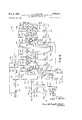
- FIG. 6 illustrates another pulse progression circuit 300 which also employs a series of neon lamps or other breakdown devices 12a, 12b and 12n. It will be understood that any desired number of additional breakdown devices may be interposed between the devices 12b and 12n.
- a direct energizing voltage is applied between positive and negative power supply terminals 302 and 304.
- a negative supply lead 306 is connected to the negative terminal 304.
- the voltage on the positive supply lead 302 may be approximately volts.
- a common resistor or impedance 308 is connected between the positive supply terminal 302 and a lead 310 from which all of the neon lamps 12a-n are energized.
- a diode 312a is connected between the lead 310 and one electrode of the neon lamp 12a.
- Diodes 312b-n are similarly connected between the lead 310 and the neon lamps 12b-n.
- Resistors 314a-n are connected between the negative supply lead 306 and the other electrodes of the neon lamps 12a-n.
- Transistors or other amplifying devices 316a-n are employed in coupling circuits 318a-n between the successive neon lamps 12a-n.
- the base of the transistor 316a is connected to the junction between the lamp 12a and the resistor 314a, so that the resistor 314a serves as a base return resistor.
- the bases of the other resistors 316b-n are similarly connected to the corresponding lamps 12b-n.
- the emitters of all of the transistors 316a-n are connected together by means of a lead 320.
- a diode 322 may be connected between the lead 320 and the negative supply lead 306 to provide a small bias, such as one volt, on the emitters.
- Load resistors 322b-n are similarly connected between the supply lead 324 and the collectors of the respective transistors 316bn.
- a voltage dropping resistor 326 may be connected between the positive supply terminal 302 and the supply lead 324.
- the resistor 326 establishes a lower voltage, such as about 45 volts, between the supply lead 324 and the negative lead 306.
- a filtering capacitor 328 may be connected between the lead 324 and the negative lead 306.
- a voltage-dividing resistor 330 is connected between the common lead 310 and the supply lead 324. Initially, the voltage on the lead 310 may be established at about 55 volts.
- the coupling circuit 318a also comprises a resistor 332a and a capacitor 334a connected in series between the collector of the transistor 316a and the junction between the diode 312b and the neon lamp 121).
- the coupling circuits 31811-11 comprise similarly connected resistors 332b-n and capacitors 334b-n.
- the common resistor 308 is of such a high value that only one of the neon lamps 12a-n can be conductive at any one time. Negative input pulses applied to the line 310 will momentarily cause all of the neon lamps to be nonconductive. Thus, if the lamp 12a is initially conductive, a negative pulse applied to the line 310 will cause the lamp 12a to become nonconductive. The resulting drop in the positive voltage on the base of the transistor 316a causes the transistor to become nonconductive. Thus, an amplified positive pulse is generated at the collector of the transistor 316a. This positive pulse is transmitted by the resistor 332a and the capacitor 334a to the next neon lamp 12b in the sequence, so as to cause this lamp to break down and become energized. The next input pulse causes the conduction to be transferred from the neon lamp 12b to the next lamp in the sequence, and so forth. Thus, successive inputpulses cause the neon lamps to be successively energized.
- the input pulses on the line 310 are generated by a circuit 340 comprising a transistor 342 having its collector connected to the line 310.
- the diode 322 is connected between the emitter of the transistor 342 and the negative lead 306. Thus, the diode 322 supplies a small emitter bias for the transistor 342.
- the normal input or counting pulses are applied between input tenminals 344 and 346.
- the terminal 346 is connected to the negative supply lead 306.
- the terminal 344- is connected to the base of the transistor 342 through a capacitor 348, a lead 350, and a resistor 352 connected in series.
- a resistor 354 may be connected between the lead 350 and the negative supply lead 306.
- Positive going input pulses at the input terminal 344 produce positive pulses at the base of the transistor 342 so as to render the transistor 342 conductive.
- the current through the collector-emitter path of the transistor 342 reduces the positive voltage on the line 310 so as to render all of the neon lamps 12a-n momentarily nonconductive.
- Output terminals 360a-n may be connected to the collectors of the transistors 316a-n. If desired, the load resistors 322a-n may be replaced with the windings of relays which may be employed to control lamps or other utilization devices.
- the input pulses applied to the terminal 334 may be derived from a clock or other timer 362 and may have the wave form indicated by the oscillogram 364. As shown, the input pulses have a magnitude of about 25 volts and a duration of about 15 microseconds.
- the illustrated counter 300 of FIG. 6 is provided with two setspulse terminals 371 and 372.
- An isolating diode 374 is connected between the terminal 371 and the lead 350 so that the first set pulse will be applied through the resistor 352 to the base of the transistor 342.
- the second setapulse terminal 372 is connected through a capacitor 376 to a flexible lead 380 which may be connected to any of the output terminals 36011-11.
- the lead 380 is connected to the output terminal preceding the neon lamp 12a-n which is to be rendered conductive.
- First and second set pulses are supplied to the first and second terminals 371 and 372 by a set-pulse generator 382 which is triggered by the ordinary input pulse, supplied to the generator 382 by the clock 362 through a gating device 384.
- a command signal is applied to the gating device 384.
- the first set pulse may be of the wave torm illustrated by the oscillogram 386, while the second set pulse may be of the wave form illustrated by the oscillogram 388. It will be seen that the first set pulse 386 begins While the ordinary input pulse is still in effect and continues for a considerable time interval after the ordinary input pulse has ended. Thus, the first set pulse maintains all of the neon lamps 12a-n nonconductive for an extended interval.
- the second set pulse 388 begins near the end of the first set pulse and continues for a short interval after the termination of the first set pulse.
- the first set pulse 386 may be of the same amplitude as the ordinary input pulse, while the second set pulse may be of greater amplitude.
- the second set pulse produces a positive pulse across the neon lamp following the output terminal to which the lead 380 is connected, so that such neon lamp is rendered conductive at the termination of the first set pulse 386.
- FIGS. 7a-9b comprise oscillograms showing the wave form of signals at various points in the pulse progression system of FIG. 6.
- FIGS. 7a and 7b include oscillograms 400a and 400b, each of which represents the wave form of the keying pulses on the lead 310.
- the oscillograms 400a and 40% are the same except that the oscillogram 4001) is produced with a much faster horizontal time base than the oscillogram 400a.
- the oscillogram 400a may be produced with a time base of .5 second per centimeter. All of the oscillo-gnams in FIGS. 7a, 8a and 9a are produced with this time base.
- the oscillogram 40% may be produced with a time base of 50 microseconds per centimeter. Thus, the pulse 40% is spread out much wider than the pulse shown in the oscillogram 400a.
- the oscillogram 400a is also shown in FIGS. 8a and 9a.
- the oscillogram 40012 is also shown in FIGS. 8b and 9b.
- FIG. 7a illustrates another oscillogram 402a which represents the wave form of the signal at one of the output terminals, such as the output terminal 360a.
- FIG. 7b includes the oscillogram 4412b which represents the same wave form drawn with a faster time base.
- the oscillograms of FIGS. 7a and 7b illustrate the manner in which the transistor 316a becomes nonconductive in response to the keying pulse.
- FIG. 8a includes an oscillogram 404a representing the wave form of the transfer pulse at the anode or positive electrode of the second lamp 12b. This is the electrode to which the coupling capacitor 334a is connected. In FIG. 8b, the same pulse is shown in the oscillogram 40417 produced with a faster time base.
- FIG. 9a includes another oscillogram 406a representing the output signal at the next output terminal 36012.
- FIG. 9b the same signal is shown in an oscillogram 406b produced with a faster time base.
- the transistor 3161 becomes conductive near the end of the keying pulse represented by the oscillogram 400a and 4001).
- FIG. 1 Resistors: Ohms 18 39K 22a-c 47K 36a-c 10K 38ac 100K Capacitors: Microfarads 30a-c .005 46 .005 Neon lamps, Type NE2.
- FIG. 2 Resistors: Ohms 18 39K 22ac 47K Capacitors: Mf. 46 .005 56a-c .005 Neon lamps, Type NE2.
- FIG. 3 Resistors: Ohms 18 39K 76a-c 100K Capacitors: M1. 46 .005 80a-c .0015 86 .1 Neon lamps, Type NE2.
- FIG. 4 Resistors: Ohms 118 10K- 122a-c 5.6K 152a-c K
- FIG. 5 Resistors: Ohms 172 10K. 1740, e 47K. 178a-h 100K. 19211-11 100K. 208 220K. 212 47K. 216 56K. 218 100K. 224 1 Meg. 230 330K. 240 1 Meg. 264 120K. 266 270K. 272 220K. 290a, e 180K. 292a, e 180K. 296a 180K.
- Capacitors Mi. 18412, f .1 1860, e .1 a-h .001 210 .005 220 .0039 232 .0039 238 .001 268 .0006 282 .022 294a, e .l
- Neons Type NE2.
- FIG. 6 Resistors: Ohms 308 220K 314a-n 100K 322a-n 47K 326 82K 330 100K 332an 100K 352 100K 354 47K Capacitors: Mf. 328 .1 334tz-n .0005 348 .0005 376 .022
- Neons Type NE2. Diodes, Type Hughes 589 Silicon. Transistors, Type TI496.
- FIG. 10 illustrates another pulse progression device 380 which is arranged to serve as an electronic counter.
- the pulse progression device 380 comprises a series of counter stages 382a-n. Two or more such stages may be employed.
- the illustrated device 380 has four stages 382a, 382b, 382a and 38211. Any desired number of additional stages may be interposed between the stages 382a and 38211. All of the stages may be substantially the same.
- the pulse progression circuit or counter 380 may be energized by a source of direct current connected between positive and negative power supply terminals 384 and 386, the negative terminal 386 being connected to ground.
- the pulse progression stages 382a-n comprises corresponding breakdown devices 388an which may be of the general type already described.
- each of the breakdown devices 388an may take the form of a neon lamp, a Shockley solid state breakdown diode, a Thyratron arc discharge tube, or various other elements or combinations of elements exhibiting breakdown characteristics of the type already discussed.
- Leads 390a-n and 392a-n extend from the opposite sides of the breakdown devices 388a-n. All of the leads 392a-n are preferably connected to a common lead 394.
- a resistor or impedance 396 is connected between the lead 394 and ground.
- the resistor 396 is of a sufficiently high value, with relation to the power supply voltage, to insure that only one of the breakdown devices 38811-11 will be conductive at any one time.
- a load resistor 398a and an isolating diode 400a are connected in series between the positive power supply lead 402 and the terminal lead 390a of the breakdown device 388a.
- the lead 402 is connected to the positive power supply terminal 384.
- An output terminal 404a is preferably connected to the junction between the load resistor 398a and the diode 400a. Coupling between the stages 382a-n is provided by a series of capacitors 406a-n. It will be seen that the capacitor 406a is connected between the output terminal 404:!
- the other coupling capacitors 406b-n are similarly arranged.
- the capacitor 406;; is connected between the output terminal 40421 and the lead 390a.
- the stages 382a-n are connected in a closed ring arrangement.
- the input pulses or other signals to be counted may be applied between an input terminal 408 and ground.
- an amplifying device in the form of a transistor 410 is employed to amplify the input pulses.
- a coupling capacitor 412 is connected between the input terminal 408 and the base of the transistor 410.
- the collector of the transistor 410 is connected directly to 13 be positive power supply lead 402.
- the emitter of the transistor 410 is connected to the lead 394 so that the resist-or 396 carries the emitter current to ground.
- a base return resistor 414 is connected between the base of the transistor 410 and ground.
- FIG. a illustrates a modification in which the breakdown devices 388a-n take the form of neon lamps or other similar gaseous discharge devices.
- a neon lamp 416a is connected between the terminal leads 390a and 392a. Similar lamps may be employed in the other counter stages.
- FIG. 10b illustrates another modification in which solid state breakdown devices are employed.
- the breakdown device 388a comprises a Shockley breakdown diode 418a connected between the lead 390a and 3920. Similar breakdown diodes may be employed in the other counter stages.
- the first breakdown device 388a is initially conductive. All of the other breakdown devices 388bn will be nonconductive due to the high value of the resistor 396 which limits the current to a value which will support conduction in only one of the breakdown devices.
- the transistor 410 is substantially nonconductive.
- Each of the input pulses renders the transistor 410 conductive between the collector and the emitter.
- the input pulses are positively polarized and the transistor 410 is of the NPN type so as to be rendered conductive by the positive pulses.
- the emitter current flows through the resistor 396 and increases the voltage drop across the resistor to such an extent that the breakdown device 388a becomes nonconductive.
- the coupling capacitor 406a transmits a positive pulse to the positive lead 39011 of the neon breakdown device 388b, with the result that the breakdown device 388b becomes conductive at the end of the input pulse.
- Each succeeding input pulse causes the conduction to be transferred to the next breakdown device in the sequence.
- the diodes 400a-n prevent the transmission of the transfer pulse to any stage other than the next stage in the sequence.
- FIG. 10 includes a diagram 422 illustrating the general wave form of the output signal at the output terminal 404m It will be understood that similar signals appear at the other output terminals 404ac.
- the horizontal line 424 represents the positive supply voltage which is the level of the signal at the output terminal 40411 when the corresponding breakdown device 388m is nonconductive.
- the breakdown device 38812 bcomes conductive, the voltage drops to a lower level 426 due to the drop in voltage across the load resistor 39811. This produces a negative going pulse 428.
- the breakdown device 383n again becomes nonconductive, the voltage at the output terminal 4041i returns to the original level.
- FIG. 11 illustrates a counter or pulse progression device 440 having breakdown devices 442a-n in the form of special electronic switching or latching circuits, each of which may comprise several circuit components.
- the pulse progression circuit 440 is arranged in a plurality of stages 444an.
- a source of direct current may be connected between positive and negative power supply terminals 446 and 448. As shown, the negative terminal 448 is connected to ground. Positive and negative supply leads 450 and 452 are connected to the terminals 446 and 448.
- the first breakdown device 442a comprises a switching transistor 454a which is coupled to an output transistor 456a.
- the two transistors 454a and 45611 are preferably of dilferent types.
- the transistor 454a is of the NPN type, while the transistor 456a is of the PNP type. This situation could be reversed, in which case the polarity of the supply voltage would be reversed.
- the collector of the transistor 454a is directly coupled to the base of the transistor 456a by a lead 458a.
- a coupling resistor 460a is connected between the collector of the transistor 456a and the base of the transistor 454a.
- a biasing resistor 462a is connected between the positive lead 450 and the collector of the transistor 454a.
- the resistor 462a is also connected through the lead 458a to the base of the transistor 456a so as to serve as a base return resistor for the output transistor 456a.
- the provision of the resistor 462a maintains cutoff bias on the output transistor 456a, particularly at elevated temperatures, when the stage 444a is nonconductive.
- a common biasing resistor 466 is connected between the positive supply lead450 and a common lead 468 extending to all of the stages 440an. It will be seen that a load resistor 470a is connected between the common lead 468 and the emitter of the output transistor 456a. Similarly, load resistors 470b-n are connected between the common lead 468 and the emitters of the corresponding output transistors 456b-n. An output terminal 472a is connected to the emitter of the output transistor 45621.
- Another load resistor 474a is connected between the collector of the output transistor 456a and the negative supply lead 452.
- An output terminal 476a is connected to the collector of the output transistor 456a.
- a series of coupling capacitors 478an are employed to connect the stages 444a-n into a closed ring.
- the capacitor 478a is connected between the emitter of the output transistor 456a and the base of the switching transistor 45412 of the next stage.
- the other coupling capacitors 478bn are similarly connected.
- all of the emitters of the switching transistors 45441-11 are provided with a common load resistor or impedance 480, connected between a common lead 482 and ground.
- the emitters of all of the switching transistors 454a-n are connected to the common lead 482.
- the resistor 480 carries the emitter current of the switching transistor for the conductive stage.
- the resulting voltage drop across the resistor 480 acts as a bias on the switching transistor of the other nonconductive stages to maintain the other switching transistors in a nonconductive state.
- a biasing resistor 484 is connected between the positive supply lead and the base of the first switching transistor 454a. The resulting positive voltage on the base of the transistor 454a renders such transistor conductive when power is first applied to the pulse progression circuit 440.
- Positively polarized input pulses may be applied to the pulse progression circuit 440 between an input terminal 486 and ground. As shown, a coupling capacitor 488 is connected between the input terminal 486 and the common emitter lead 482. Thus, the positive input pulses are applied to the emitters of the switching transistors 454a-n.
- stage 444a is conductive initially. Both transistors 454a and 456a are conductive.
- the first positive input pulse raises the voltage of the emitter of the switching transistor 454a to such an extent that the transistor 454a is rendered nonconductive.
- all of the other switching transistors 454b-n are maintained nonconductive.
- the collect-or current of the switching transistor 45411 is also the 15 base current of the output transistor 456a.
- the output transistor 456a is also rendered nonconductive. This reduces the positive voltage on the base of the switching transistor 454a so that the switching transistor is latched in a nonconductive state.
- the stopping of conduction between the emitter and the collector of the output transistor 456a causes a rise in the positive voltage at the emitter, with the result that a positive pulse is transmitted by the capacitor 478a to the base of the next switching transistor 45412.
- This transfer pulse causes the switching transistor 45412 to become conductive, so that the conduction is transferred from the first stage 444a to the second stage 44412.
- the output transistor 456b also becomes conductive, due to the current from the base of the output transistor 45612 to the collector of the switching transistor 454b.
- the collector current of the transistor 45612 provides a positive bias on the base of the switching transistor 454b, so that the switching transistor is latched in a conductive condition.
- each input pulse causes the conduction to transfer from the conductive stage to the next stage in the sequence.
- Each input pulse is differentiated by the capacitor 488 and the resistor 480 so that the off pulse which appears across the resistor 480 represents the dilferential of the leading slope or rise of the input pulse.
- the duration of the input pulse is not critical and may be anything from a design minimum of about one microsecond to infinity.
- Successive input pulses cause the successive stages of the pulse progression circuit to become conductive. Only one stage is conductive at any one time, so that the power consumption of the pulse progression circuit is extremely low. This is a distinct advantage, particularly when the power is derived from a battery, as in the case of portable equipment.
- most prior counters such as flip-flops, at least a portion of each stage is conductive at all times. Thus, in the case of a flip-flop, one-half or the other of the stage is conductive at all times.
- FIG. 11a comprises an oscillogram 494 of typical input pulses.
- FIG. 11a also includes oscillograms 496 and 498 showing the general wave form of the output signals at the output terminals 472b and 476b. It will be seen that the output wave form 496 at the output terminal 472b is in the form of a negative-going pulse, while the wave form at the output terminal 47612 comprises a positive-going pulse. These pulses correspond to the time interval during which the transistor 45612 is conductive.
- the horizontal line 500 represents the 13-]- level, or the positive voltage of the power supply on the lead 450.
- the line 502 represents the zero level at ground.
- the output transistor 456b When the output transistor 456b is nonconductive, the voltage at the output terminal 47212 is at a level 504 which is slightly lower than the B+ level 500, by the amount of the biasing drop across the resistor 466.
- the output transistor 456k When the output transistor 456k is conductive, the voltage at the output terminal 47212 drops by the amount of the voltage drop across the load resistor 47012, due to the emitter current of the transistor 45612.
- the output transistor 45612 When the output transistor 45612 is nonconductive, the voltage at the output terminal 47612 is at the zero level 502. When the switching transistor 456b becomes conductive, the voltage at the output terminal 47612 rises to a positive value corresponding to the voltage drop through the output resistor 47412 due to the collector current of the transistor 456b. It will be understood that the output wave form 496 constitutes the emitter voltage of the output transistor 45612, while the output wave form 498 constitutes the collector voltage of the output transistor. When the output transistor 456b is conductive, the small difference between the emitter and collector voltages 496 and 498 corresponds to the small drop between the emitter and the collector of the output transistor. In FIG.
- the capacitor 47811 may be omitted because the biasing resistor 484 will cause the first stage 444a to become conductive after the last stage 44411 becomes nonconductive.
- the biasing resistor 466 may be omitted in many cases, particularly if silicon transistors are employed in the pulse progression circuit. In that case, the lead 468 is connected directly to the positive supply lead 450.
- the base return resistors 462a-n may also be omitted if silicon transistors are employed. In that case, the resistors 462an are simply removed, without any other change in the connections.
- the pulse progression device or counter 440 of FIG. 11 has the additional important advantage that the device may be set to any desired count, simply by applying a setting pulse or voltage of sufficient magnitude and duration to the output terminal 476 of the stage corresponding to the desired count.
- the first stage 444a may be rendered conductive by applying a sufficiently great positive setting voltage or pulse to the output terminal 476a.
- the setting pulse may be derived from a setting pulse generator 507 and may be applied to the output terminal 476a by a movable contact or lead 509.
- the setting voltage should be greater than the normal output voltage from the counter.
- the setting voltage picks up the collector of the output transistor 456a and causes current to flow through the resistor 460a to the base and then to the emitter of the switching transistor 454a.
- the switching transistor 454a is rendered conductive.
- the output transistor 456a is also conductive. Due to the mutual latching action of the transistors 454a and 456a, the stage 444a is latched in a conductive state.
- the stage which was previously conductive is rendered nonconductive.
- the second stage 444b was previously conductive.
- the application of the setting voltage to the first stage causes the fiow of sufficient emitter current in the first switching transistor 454a to render the second switching transistor 45% nonconductive by virtue of the increased voltage across the common emitter resistor 480.
- the second stage is turned ofi? in much the same manner as when an input pulse causes an increase of voltage across the common emitter rcsistor 480.
- a transfer pulse is applied to the next stage 44421 so as to cause it to become conductive momentarily.
- the stage 44411 cannot latch in a conductive state because of the increased voltage across the common emitter resistor 480 due to the emitter current of the first switching transistor 454a, produced by the setting voltage applied to the output terminal 476a.
- the stage 444n returns to a nonconductive state when the transfer pulse dies out.
- the setting voltage may then be removed from the output terminal 476a.
- the duration of the setting voltage should substantially exceed the duration of the transfer pulse.
- the duration of the transfer pulse is dependent upon the time constant of the interstage coupling circuits of the counter.
- the counter 440 of FIG. 11 has the additional important advantage that it is readily possible to cause the counter to skip a stage, simply by short-circuiting the collector output resistor 474 of the stage to be skipped. Thus, if the second stage 444b is to be skipped, the output terminal 47512 is short-circuited to ground. When this is done, the counter skips over the second stage from the first stage to the third stage.
- the various stages 440a-n may be provided with short-circuiting switches or contacts 511a-n connected across the load resistors 474a-n.
- the short-circuiting of the collector resistor 4741 prevents the stage 4441; from latching in a conductive state. Instead, the stage 4441) becomes conductive only momentarily when it receives a transfer pulse from the first stage. Thus, the second stage serves merely as a coupling device between the first and third stages.
- the transistors 45 3b and 4561 become conductive.
- the emitter-collector current in the output transistor 45611 is somewhat greater than usual, due to the short-circuiting of the collector resistor 474.1).
- the short-circuiting of the resistor 474D prevents any latching current from flowing through the resistor 46%! to the base of the switching transistor 4541;.
- the transistors 45419 and 45611 become nonconductive.
- the termination of conduction in the output transistor 45611 produces a transfer pulse which is supplied to the next stage so that it is rendered conductive.
- the counter may be employed to control a series of functions of an illuminated sign or some other apparatus. At times it may be desirable to omit one function controlled by one of the stages of the counter. This may be done simply by short-circuiting the output of such stage, whereupon the counter will skip the stage.
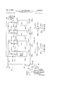
- FIG. 12 illustrates the basic latching or switching circuit which is employed as a breakdown device in the pulse progression circuit of FIG. 11.
- the circuit of FIG. 12a will be designated 510.
- the latching circuit 510 is arranged in virtually the same manner as each of the stages 444(1-12 of the pulse progression circuit of FIG. 11, with only a few minor differences.
- the emitter load resistor 470:: is connected directly to the positive power supply lead 450 in the latching circuit 510 of FIG. 12a.
- a biasing diode 512 is connected, in series with the emitter return resistor 480. This biasing diode may often be omitted, particularly if silicon transistors are employed.
- the latching circuit 510 may have an input terminal 514. It will be seen that a coupling capacitor 516 is connected between the input terminal 514 and the base of the switching diode 454a.
- the input terminals 486 and 514 provide two alternative inputs which make it possible to obtain opposite responses from pulses of the same polarity.
- a positive pulse applied to the input terminal 514 will cause both of the transistors 454a and 456a to become conductive.
- a positive pulse, when applied to the input terminal 486, will cause the transistors 454a and 45st; to become nonconductive.
- a negative pulse when applied to the input terminal 486, will cause the transistors 454a and 456a to become conductive.
- a negative pulse will cause both transistors to become nonconductive.
- the switching transistor 454a becomes conductive when its base is driven substantially more positive than its emitter.
- the collector current of the transistor 454a causes the'base of the output transistor 456a to be driven negative relative to its emitter, so that the transistor 456a also becomes conductive.
- the switching transistor $5M is of the NPN type, while the output transistor 456a is of the PNP type.
- the switching transistor 454a may be rendered nonconductive by driving its base negative relative to its emitter.
- the loss of the collector current of the transistor 454a causes the base of the output transistor 456:: to go positive relative to the emitter, so that the transistor 456a also becomes nonconductive.
- the positive 1% bias on the base of the switching transistor 454a drops to zero so that the switching transistor 454a is latched in a nonconductive state.
- the diode 512 assists the latching action by providing a small positive bias on the emitter of the switching transistor 454a.
- the output terminals 472a and 476a provide output signals of opposite phase polarity.
- a negativegoing pulse 529 is produced at the output terminal 472a
- a positive-going pulse 522 is produced at the output terminal 476a.
- the input terminals 514 and E36 may be employed to provide a pushpull input
- the output terminals 472:: and 476a may be employed to provide a push-pull output.
- FIG. 12b illustrates a trigger circuit 531) which is a modification of the latching circuit 510.
- the trigger circuit 530 has a pulse sharpening and squaring action, so that a single brief pulse of substantially square wave form is produced in response to each input pulse.
- the trigger circuit 530 is very similar to the latching circuit 510, with only a few changes.
- a capacitor 532 is connected in series with the resistor 460a between the collector of the output transistor 456a and the base of the switching transistor 454a. By virtue of the capacitor 532, the transistor 454a is latched only briefly in its conductive state. As soon as the capacitor 532 becomes charged, the latching action is lost.
- the switching transistor 454a then returns to its nonconductive state due to the drop across the emitter resistor 480 and the biasing diode 512.
- a return resistor 534 is connected between the base of the transistor 454a and ground.
- the resistor 534 may be shunted with a reversely polarized diode 536 to speed up the discharge of the capacitor 532 after the output transistor 456a becomes nonconductive.
- the input terminals 514 and 486 are adapted to receive positive and negative input pulses, respectively, which may be of rather rounded Wave form, as indicated by the oscillogra-ms 538 and 540.
- the trigger circuit 530 is operative in response to either or both of the input pulses 538 and 540.
- the trigger circuit 530 In response to each input pulse, the trigger circuit 530 produces a single brief output pulse of substantially square wave form. At the output terminal 472a, the output pulse is of negative-going polarity, as indicated by the oscillogram 542. At the output terminal 476a, the output pulse is of positive-going polarity, as indicated by the oscillogram 544.
- FIG. 12c illustrates a pulse generator 550 constituting another variation of the basic latching circuit 510 of FIG. 12a.
- the pulse generator circuit 550 is made self-exciting by connecting a fixed resistor 552 and a variable resistor or potentiometer 554 in series between the collector and the base of the switching transistor 454a. These resistors 552 and 554 tend to drive the base positive so as to render the switching transistor 454a conductive.
- the circuit between the collector of the output transistor 456a and the base of the switching transistor 454a is modified to include not only the resistor 460a but also a variable resistor or potentiometer 556- and a selective capacitor circuit 558, the variable resistor 556 and the capacitor circuit 558 being in series with the resistor 460a.
- the capacitor circuit 558 comprises a switching member 560 which is movable into engage ment with any one of three contacts 561, 562 and 563. Three capacitors 566, 567 and 568 of different values are connected between the respective contacts 561-3 and a common lead 570.
- the variable resistor 556 is connected between the common lead 570 and the collector of the output transistor 456a. The position of the switch 560 offsets both the width and the frequency of the output pulses.
- the emitter of the 19 transistor 454a is returned directly to ground by a lead 574.
- a resistor 576 is interposed in the lead 458a between the base of the output transistor 456a and the collector of the transistor 454a.
- the base of the switching transistor 454a is substantially at ground potential so that the transistor 454a is nonconductive.
- the capacitor 567 is in the circuit.
- the application of the positive power supply to the terminal 446 causes the capacitor 567 to become charged through the resistors 462a, 554, 552, 460a, 555 and 474a.
- the charging time constant is proportional to the total resistance of these resistors and the capacitance of the capacitor 567.
- the capacitor is charged to such an extent that the base of the transistor 454a becomes sufiiciently positive to render the transistor conductive.
- the output transistor 456a in turn becomes conductive due to the collector current of the transistor 454a, which drives the base of the output transistor 456a negative relative to its emitter.
- the switching transistor 454a When the switching transistor 454a becomes conductive, the collector voltage drops to a very low value due to the direct connection of the emitter to ground. Thus, the capacitor 567 begins to discharge through the baseemitter path of the transistor 454a.
- the collector current of the output transistor 456a produces a positive voltage across the load resistor 474a which tends to charge the capacitor 567 with a polarity opposite from its original charge.
- the capacitor 567 charges through the resistors 556 and 460a and the base-emitter path of the transistor 454a.
- the charging time constant is proportional to the total resistance and the capacitance of the capacitor 567. While the capacitor 567 is being charged by the voltage across the resistor 474a, the conduction in the transistor 454a is maintained by the charging current. Once the capacitor 567 becomes fully charged, the transistor 454a becomes nonconductive.
- the pulse generator 550 produces a train of negative-going pulses 580 representing the intervals of conduction of the output transistor 456a.
- the pulses 580 are relatively brief and are seperated by the longer intervals during which the output transistor 456a is nonconductive.
- the width or duration of the pulses 580 depends upon the time constant represented by the capacitance of the capacitor 567 and the total resistance of the resistors 460a and 556.
- the width or duration of the pulses 580 may be varied by adjusting the variable resistor 556.
- the interval between the pulses 580 is determined by the time constant of the capacitor 557 and the total resistance of the resistors 462a, 554, 552, 460a, 556 and 474a.
- the interval between the pulses may be adjusted by varying the variable resistor 554.
- the output signal com-prises narrow positive-going pulses 582 corresponding to the pulses 580. Between the pulses 582, the charging of the capacitor 567 produces a slope 584.
- the trigger circuit 530 and the pulse generator 550 are extremely useful variations of the basic latching circuit 510. These circuits have the advantage that they are not sensitive to variations in the supply voltage and in the values of the circuit components. Thus, the circuits will operate in a positive manner over a wide range of supply voltages. Moreover, the values of the circuit components need not be maintained with a high degree of precision.
- the pulse progression circuits of the present invention utilize breakdown devices which are connected in sequence and are successively rendered conductive in response to the successive input pulses.
- the breakdown devices may be in the form of gaseous discharge lamps, arc discharge tubes, solid-state breakdown diodes or triodes, latching circuits, or other devices having the ability to become abruptly conductive in response to a change in the applied voltage, without the need for any change of polarity.
- the input pulses render all of the breakdown devices nonconductive momentarily.
- the breakdown devices are coupled together in such a manner that the interruption of conduction in any of the breakdown devices will produce a transfer signal which causes the next breakdown device in the sequence to become conductive at the end of the input pulse.
- the pulse progression circuits of the present invention require only one breakdown device for each stage of the circuit.
- the breakdown devices may usually be in the form of small neon lamps.
- the cost of the breakdown devices is very small.
- a single transistor will provide good coupling between successive stages.
- the number and cost of the active electronic components per stage may be very low.
- the pulse progression circuits may readily be arranged to provide counters operating with any desired number as the counting base.
- the present invention results in electronic counters having remarkably few active electronic components to achieve a desired total count.
- the present invention is very advantageous to provide counters, stepping switches, cascade generators, and the like.
- each of said breakdown devices comprising a switching transistor and an output transistor coupled to said switching transistor for latching said switching transistor in both conductive and nonconductive states
- said switching transistor also latching said output transistor in conductive and nonconductive states corresponding to said conductive and nonconductive states of said switching transistor, an energizing circuit connected to said breakdown devices and including an impedance common to all of said switching transistors for limiting conduction in said breakdown devices to only one device at any one time, an input circuit responsive to an input pulse for stopping conduction in all of said breakdown devices,
- coupling means connected between said devices in sequence and including means for producing a transfer signal in response to the stopping of conduction in any one of said devices for initiating conduction in the next device in the sequence
- setting means for selectively applying a setting signal to one of said breakdown devices for latching said transistors thereof in a conductive state, said setting signal having a duration greater than said transfer signal.
- each of said breakdown devices comprising a transistor latching circuit having a switching transistor
- one of said transistors being NPN and the other PNP,
- an energizing circuit connected to said breakdown devices and including an impedance common to the switching transistors of all of said devices for limiting conduction in said devices to only one device at any one time
- each coupling device being connected between the output transistor of one breakdown device and the switching transistor of the next breakdown device
- said coupling devices producing transfer signals in response to the interruption of conduction in any of said output transistors for initiating conduction in the next switching transistor
- said breakdown devices thereby being rendered successively conductive by successive input pulses
- each of said breakdown devices comprising a transistor latching circuit having a switching transistor
- one of said transistors being NPN and the other PNP,
- an energizing circuit connected to said breakdown devices and including an impedance common to the switching transistors of all of said devices for limiting conduction in said devices to only one device at any one time
- each coupling device being connected between the output transistor of one breakdown device and the switching transistor of the next breakdown device
- said coupling devices producing transfer signals in re sponse to the interruption of conduction in any of said output transistors for initiating conduction in the next switching transistor
- said breakdown devices thereby being rendered successively conductive by successive input pulses
- each of said breakdown devices comprises an output impedance connected to the corresponding output transistor
- said setting means is c-onstructed and arranged to apply the setting signal to the output impedance of a selected one of said breakdown devices for latching said transistors thereof in a conductive state.
- said transistors comprise a plurality of electrodes
- each of said breakdown devices comprises an output impedance connected to one electrode of the corresponding output transistor
- said setting means being constructed and arranged for selectively applying the setting signal to one of said output impedances for latching the transistors of the corresponding breakdown device in a conductive state.
- said breakdown devices comprise respective output impedances connected to the corresponding output transistors
- said transistors comprise a plurality of electrodes
- each of said breakdown devices comprises an output impedance connected to one electrode of the corresponding output transistor
- said short circuiting switches being connected across said output impedances to cause the selected breakdown device to be skipped in the sequence of conduction.
Landscapes
- Circuit Arrangements For Discharge Lamps (AREA)
- Control Of Indicators Other Than Cathode Ray Tubes (AREA)
Description
1966 s. A. PROCTER 3,290,515
CONTROLLED PULSE PROGRESSION CIRCUITS WITH COMPLEMENTARY TRANS I STORS 7 Sheets-Sheet 1 Filed May 28, 1963 INVENTOR.
Samuel A Prode!" 1966 s. A. PROCTER 3,29@,5'l5
CONTROLLED PULSE PROGRESSION CIRCUITS WITH COMPLEMENTARY TRANSISTORS Filed May 28, 1965 7 Sheets-Sheet z Bu 0% 7 I ATTORNEYS Dec. 6, 1966 s. A. PROCTER 3,290,515
CONTROLLED PULSE PROGRESSION CIRCUITS WITH COMPLEMENTARY TRANSISTORS Filed May 28, 1965 '7 Sheets-Sheet 5 INVENTOR. Samuel A.Pho I" BY @vrw y cflaz wam Wk A++or-neus Fund? hum msoomL zww Fmm AMQMMQ wzamummm # 250 or 1966 s. A. PROCTER 15 CONTROLLED PULSE PROGRESSION CIRCUITS WITH COMPLEMENTARY TRANSISTORS Filed May 28, 1963 7 Sheets-Sheet 4 I I I I I l I i l l I I i I 4006L -.-.T. A
mm/L J 4021 F I 6. 7(1 FIG. 7D
4041* v-'I 1,-- l I -r FIG. 8a FIG 8b INVENTOR. Samud A, Procter BY @7714 990M M W /ac Afior-neqs Dec. 6, 1966 s. A. PROCTER CONTROLLED PULSE PROGRESSION CIRCUITS WITH COMPLEMENTARY TRANS S TORS 7 Sheets-Sheet 5 Filed May 28, 1963 INVENTOR. Samuel A. Pmder A Torneqs Dec. 6, 1966 s. A. PROCTER CONTROLLED PULSE PROGRESSION CIR 3,2 90,515 GUITS WITH COMPLEMENTARY TRANS I STORS '7 Sheets-Sheet 6 Filed May 28, 1963 Dec, O, 1966 s PROCTER 3,290,515
CONTROLLED PULS E PROGRESSION CIRCUITS WITH COMPLEMENTARY TRANS I S TORS Filed May 28, 1963 7 Sheets-Sheet 7 4 4a U OFF OFF INVENTOR. Samuel A. Proc+er- 00 BY M Q% 027a United States Patent 3,290,515 CONTROLLED PULSE PROGRESSION CIRCUITS WITH CUMPLEMENTARY TRANSISTORS Samuel A. Procter, 1936 Cedar Lake Blvd., Minneapolis, Minn. Filed May 28, 1963, Ser. No. 283,940 7 Claims. (Cl. 307-885) This invention relates to new and improved pulse progression circuits which will find important applications to electronic counters, electronic stepping switches, cascade generators, and electronic devices for indicating the occurrence of events per unit time, to cite only a few examples.
One object of the present invention is to provide new and improved circuits comprising a plurality of electronic devices which are rendered successively conductive by successive input pulses.
A further object is to provide new and improved circuits of the foregoing character which utilize electronic breakdown devices, such as neon or other gaseous discharge lamps, are discharge tubes such as T-hyratro'ns, transistor latching circuits, or various types of solidstate devices, such as Shockley diodes, for example.
It is a further object to provide new and improved circuits of the foregoing character which are adapted generally to employ any breakdown device which has the ability to change from a substantially nonconductive state to a conductive state in response to a change in the applied voltage, but without any change in polarity, and to remain conductive at a voltage substantially lower than that required for initiation of conduction.
Another object is to provide new and improved pulse progression circuits utilizing a plurality of electronic breakdown devices connected in sequence or cascade by a plurality of coupling devices, which may include capacitors, transformers, or transistors, for example.
A further object is to provide new and improved pulse progression circuits of the foregoing character having means whereby only one of the breakdown devices can be conductive at any one time.
Another object is to provide new and improved pulse progresson circuits having a plurality of electronic breakdown devices connected in sequence by a plurality of coupling devices, together with an impedance common to all of the breakdown devices, so that only one of the devices can be conductive at any one time, and means responsive to an input pulse for rendering the conductive device nonconductive, the coupling devices being effective to produce a transfer signal which initiates conduction in the next breakdown device in the sequence, in response to the stopping of conduction in the initially conductive device, so that successive input pulses cause the breakdown devices to be successively conductive.
Another object is to provide a new and improved pulse progression circuit which may readily be arranged to provide a counter, operating with any number as the counting base, said counter generally having considerably fewer electronic components than other types of counters, such as flip-flop circuits utilizing transistors.
A further object is to provide new and improved counter or other pulse progression circuits having a sequence of stages which become conductive successively, only one of the stages being conductive at one time, so that the current consumption of the counter is greatly reduced, particularly when compared with counters using flip-flops.
Another object is to provide a new and improved transistor latching or switching circuit for use in counters, pulse progression circuits, or other electronic devices.
A further object is to provide variations of the tran- 3 ,290,515 Patented Dec. 6, 1966 sistor latching circuit for use as trigger circuits and pulse generators.
Further objects and advantages of the present invention will appear from the following description, taken with the accompanying drawings, in which:
FIG. 1 is a schematic circuit diagram of a pulse progression circuit to be described as an illustrative embodiment of the present invention.
FIG. 2 is a fragmentary circuit diagram showing a modified pulse progression circuit utilizing coupling transformers between the electronic breakdown devices.
FIG. 3 is a circuit diagram of another modified pulse progression or counter circuit employing transistors in the coupling circuits between the electronic breakdown devices.
FIG. 4 is a circuit diagram illustrating another pulse progression circuit utilizing grid controller arc discharge tubes as the electronic breakdown devices.
FIG. 5 is a circuit diagram of another modified pulse progression circuit arranged to provide a device which counts events per unit time.
FIG. 6 is a circuit diagram of another pulse progression circuit utilizing transistors in the coupling circuits between the electronic breakdown device's.
FIGS. 7a, 7b, 8a, 8b, 9a, and'9b comprise oscillograms illustrating the wave form of various signals in the circuit of FIG. 6.
FIG. 10 is a circuit diagram of another pulse progression circuit constructed in accordance with the present invention.
FIGS. 10a and 10b are fragmentary circuit diagrams illustrating modifications of FIG. 10 utilizing different breakdown devices.
FIG. 11 is a circuit diagram of another pulse progression circuit utilizing special transistor latching circuits as the breakdown devices.
FIG. 11a comprises oscillograms showing the wave forms of input and output signals for the circuit of FIG. 11.
FIG. 12a is a circuit diagram showing the transistor latching or switching circuit as employed in FIG. 11.
FIG. 12]) is a circuit diagram showing a modification of FIG. 12a to provide a trigger circuit.
FIG. is a circuit diagram of another modification of FIG. 12a to provide a self-excited pulse generator.
As already indicated, FIG. 1 illustrates a pulse progression circuit 10 which constitutes an illustrative embodiment of the present invention. The illustrated circuit 10 may be characterized as an elementary counter circuit. The pulse progression or counter circuit 10 comprises a plurality of electronic breakdown devices. The
illustrated circuit 10 utilizes three such breakdown devices which will be designated 12a, 12b, and 120 for convenient identification. However, it will be realized that any suitable number of break-down devices may be employed, according to the number which is to be employed as the counting base. Thus, the illustrated counter is adapted to count to the base 3.
The illustrated electronic breakdown devices 12a-12c take the form of small neon glow discharge lamps, but various other types of electronic breakdown devices may be employed. Thus, the neon lamps may be replaced with other types of gaseous discharge lamps or tubes, are discharge lamps or tubes, or solid state devices such as Shockley diodes or controlled irectifiers. In general, any such breakdown device should have the ability to change from a non-conductive state to a conductive state in response to a change in the voltage applied to the device, but without any need for a change in polarity, and the device should be able to maintain conduction at a voltage lower than the voltage required for breakdown or initiacircuit 24a in detail.
tion of conduction. Of course, neon or other gaseous discharge lamps have these characteristics. Moreover, neon lamps are readily available and low in cost. Thus, neon lamps are well suited for use in the pulse progression circuit of FIG. 1. The neon lamps may be small in size and of the type commonly used for small pilot lamps.
The neon lamps 12a-12c are adapted to be energized by a battery 14 or some other source of direct current. In this case, the negative terminal of the direct-current source 14 is grounded, while the positive terminal is connected to 'a positive supply lead 16.
The energizing circuit for the neon lamps 12a-12c comprises a common resistor or impedance 18 which in this case is connected between ground and common lead 20 extending to one terminal of each of the neon lamps 12a-12c. Thus, any current which passes through any of the lamps must pass through the resistor 18. Load resistors 22a, 22b, and 220 are connected between the respective lamps 12a-12c and the positive lead 16.
The common resistor 18 is made of such a high value of resistance that only one of the neon discharge lamps 12a-12c can be conductive at any one time. A minimum current is required to maintain the electron discharge in any of the neon lamps. The resistance value of the resistor 18 is made sufficiently great, with reference to the supply voltage, to limit the current through the resistor to a value substantially less than twice the minimum discharge current for each lamp, so that the discharge can be maintained in only one lamp at a time.
The breakdown devices 12a-12c are connected in sequence or cascade by a series of coupling circuits 24a, 24b, and 240. Thus, each coupling circuit 24ac is connected between the corresponding breakdown device 12a-c and the next breakdown device in sequence. The coupling circuit 240 is connected between the breakdown device 120 and the breakdown device 12a so that the circuit forms a closed ring.
The pulse progression device is provided with an input circuit 40 for momentarily interrupting conduction in all of the breakdown devices 12a-c in response to each input pulse. In this case, the input pulses are applied across input terminals 42 and 44. A coupling capacitor 46 is connected between the input terminal 42 and the common lead 20. The other input terminal 44 is grounded. The input pulses are positive in polarity. Each of the input pulses is great enough in magnitude to reduce the voltage across the conductive lamp to a value which is insufficient to maintain the discharge in the lamp. Thus, if the neon lamp 12a is initially conductive, the input pulse renders the lamp 12a non-conductive. The coupling circuit 24a generates a transfer pulse which is supplied to the next lamp 12b in response to the stoppage of conduction in the first lamp 12a. The input pulse is short in duration so that the transfer pulse causes the second lamp 12b to break down into conduction. In the same way, the next input pulse causes the conduction to transfer from the second lamp 12b to the third lamp 120. Thus, the lamps are successively energized in response to successive input pulses.
In the coupling circuits 24a-c of FIG. 1, the transfer pulses are produced primarily by the load resistors 22a-c and the capacitors 30a-c. Thus, when the lamp 12a is conductive, the capacitor 30a is charged to a voltage corresponding to the voltage drop across the load resistor 12a. When the input pulse renders the lamp 12a non-conductive, the voltage across the capacitor 30a is applied to the second lamp 12b through the diode 24a and the resistor 36a, so as to increase the total voltage across the second lamp. Thus, conduction is initiated in the second lamp 12b at the end of the input pulse. The capacitor 30a discharges through the resistors 22a and 38a. The second capacitor 30b is charged through the load resistor 22b and the resistor 38b. The diodes 34a-c cause the lamps 12a-c to be energized in the correct sequence and not in the reverse sequence. At each of the output terminals 28a-28c, a large output pulse is produced for every third input pulse. Thus, the pulse progression circuit 10 is adapted to count to three .repeatedly. If a higher count is desired, successive ring counters may be connected in cascade. Thus, any of the output terminals 28ac may be connected to the input terminal of another ring counter. Likewise, one of the output terminals of the second ring counter may be connected to the input terminal of a third ring counter, etc.
FIG. 2 illustrates a modified pulse progression circuit 50 which is similar to the circuit 10 of FIG. 1 except that the circuit 50 employs modified coupling circuits 52a-c in place of the circuits 24a-c. All of the coupling circuits 52a-c are the same, so that only the coupling circuit 52b may be described in detail. It will be seen that the coupling circuit 52b comprises a pulse transformer 54b and a capacitor 56b. The transformer 54b is of the auto-transformer type, having a tap 58b and end terminals 60b and 62b. The tap 58b divides the transformer 54b into two portions, 64b and 66b. The primary portion 64b, between the tap 58b and the end terminal 60b, has a relatively small number of turns, while the secondary portion 66b has a much larger number of turns. In this case, the load resistor 22b is connected to the end terminal 60b, while the tap 58b is connected to a lead 68b extending to one electrode of the neon lamp 12b. Thus, the load resistor 22b and the primary portion 64b of the transformer 54b are connected in series between the positive supply lead 16 and the neon lamp 12b. The capacitor 56b is connected between the other end terminal 52b and the lead 680 which extends to the next lamp 120. Thus, the secondary portion 66b of the transformer 54b is connected in series with the capacitor 56b to the next lamp 12c.
When the lamp 12b is conductive, the discharge current through the lamp also flows through the primary portion 64b of the transformer 54b. When the next input pulse renders the lamp 12b non-conductive, the interruption of the current through the primary winding 64b generates a high voltage pulse in the secondary winding 66b. This pulse is transmitted to the next lamp 120 and causes it to become conductive at the end of the input pulse. Because of the step-up effect of the transformer in each coupling circuit, the pulse progression circuit of FIG. 2 has improved reliability so that it is insensitive to variations in the characteristics of the neon lamps, the supply voltage, and the values of the various resistors and capacitors.
FIG. 3 illustrates another modified pulse progression circuit 70 which is similar to the circuit 10 of FIG. 1, except that the circuit 70 comprises modified coupling circuits 72a-c utilizing amplifying devices 74a-c. As shown, the amplifying devices 74a-c take the form of transistors, but vacuum tubes or other amplifying devices may be employed. All of the coupling circuits 72a-c are the same, so that only the coupling device 72a need be described in detail. A load resistor 76a is connected between the positive supply lead 16 and the collector of the transistor 74a. The emitter of the transistor 74a is connected to a lead 78a which extends to one electrode of the neon lamp 12a. A coupling capacitor 80a is connected between the collector of the transistor 74a and the emitter of the transistor 74b for the next lamp 1217. An output terminal 82a may be connected to the collector of the transistor 74a.
The bases of all the transistors 74a-c are connected together by a common lead '84. A filtering or bypass capacitor '86 is connected between the lead 84 and ground.
It may be assumed that in the initial state of the circuit of FIG. 3, the neon lamp 12a is conductive while the other lamps 12b and 12c are not conductive. The common resistor 18 prevents conduction in more than one lamp at any one time. It will be observed that the transistor 74a is arranged with its collector-emitter path in series with the lamp 12a. Thus, the transistor 74a is conductive when the lamp 12a is conductive. The drop across the transistor is quite small, usually less than one v-olt. The base, emitter, and collector of the transistor 74a are all at about the same potential. Thus, the base of the transistor 74a assumes a voltage which is substantially equal to the total voltage drop across the lamp 12a and the resistor 18, plus the small drop across the transistor. By way of example, the voltage at the base of the transistor 74a may be about 62 volts with a power supply potential of 90 volts. The drop across the resistor 18 may be about 12 volts. The capacitor 86 is large enough to prevent any rapid changes in the voltages on the bases of the three transistors 74a-c. Thus, the base voltage remains at all times at about 62 volts.
As before, the positive input pulses are applied across the common resistor 18. The input pulses may have a magnitude of perhaps 20 volts, for example. The first pulse causes the lamp 12a to become non-conductive, so that all of the lamps are non-conductive momentarily. The interruption of the emitter current in the transistor 74a also causes interruption of the collector current, so that the voltage at the collector rises rapidly to the full 90 volts of the power supply. This pulse of voltage is applied by the capacitor 80a to the next lamp 12b, which thus is rendered conductive. The next input pulse transfers the conduction to the lamp 12c, etc., around the ring. It will be recognized that each transistor acts as a switch for its own lamp and as an amplifier or transfer device to trigger the next lamp in the sequence.
In the circuits of FIGS. l-3, the lamp 12a is energized when the count is zero, three, six, etc. The lamp 121; becomes conductive when the count is 1, 4, 7, etc. The lamp 12c is energized when the count is 2, 5, 8, etc.
FIG. 4 illustrates a modified pulse progression circuit 110 which employs breakdown devices 112a-c, illustrated as grid-controlled arc discharge tubes, such as thyratrons, for example. It will be realized, however, that other types of breakdown devices may be employed, such as controlled solid state rectifiers, for example. The energizing voltage for the thyratrons 112ac is applied between ground and a positive supply lead 116. A common resistor or impedance 118 is connected between ground and a lead 120 which is connected to the cathodes of all three thyratrons 112ac. It will be realized that any desired number of thyratrons may be employed, according to the number which is to be utilized as the counting base. The resistor 118 is sufficiently high in value to insure that only one of the thyratrons 112a-c will be conductive at a time.
Load resistors 122a-c are connected between the positive supply lead 116 and the plates of the respective thyratrons 112a-c.
As before, positive input pulses are applied across the common resistor 118 by means of a capacitor 146 connected to an input terminal 142, the input terminal 144 being grounded.
Output terminals 128a-c may be connected to the plates of the thyratrons 112a-c. Coupling circuits or devices 124a-c are provided between the successive thyratrons 112ac. All of the coupling circuits 124a-c may be the same, so that only the coupling circuit 124a need be described in detail. This circuit comprises a capacitor 150a connected between the plate of the thyratron 6 112a and the control grid or electrode of the thyratron 1121). A grid resistor 152a is connected between the grid of the thyratron 112 b and ground.
It may be assumed initially that the thyratron 112a is conductive, while the other thyratrons 11211 and 1120 are not conductive. The first positive input pulse at the cathode of the thyratron 112a reduces the voltage between the plate and cathode to such an extent that the thyratron 112a becomes non-conductive. The rapid rise in the positive voltage at the plate of the thyratron 112a produces a positive voltage pulse which is transmitted by the capacitor a to the control grid of the next thyratron 112k. Thus, the thyratron 112b becomes conductive. Similarly, the next input pulse transfers the conduction to the thyratron 1120, and so forth around the ring. a
FIG. 5 illustrates another pulse progression circuit which constitutes an elaboration of the circuit of FIG. 3, particularly adapted for counting events per unit time. The circuit 116 comprises two ring counter stages 162 and 164 connected in cascade. Each counter stage employs four breakdown devices, so that a total count of 16 may be registered. Thus, the first counter stage 162 comprises breakdown devices in the form of neon lamps 12a-a'. The counter stage 164 comprises four additional neon lamps 12c-h.
The two ring counters 162 and 164 are substantially the same so that only the ring counter 16-2 need be described in full detail. Direct current for energizing the circuit is derived from a battery or other source 166 having its negative terminal grounded. The positive terminal of the battery 166- is adapted to be connected to a positive supply lead 168 through a switch 170 connected in series with a variable resistor 172. Thus, the voltage between the supply lead 168 through a switch 170 connected in series with a variable resistor 172. Thus, the voltage between the supply lead 168 and ground may be changed by varying the resistor 172.
A common resistor or impedance 174a is connected between ground and a lead 176a connected to one side of each of the neon lamps 12a-a'. Load resistors 178ad are connected between the supply lead 168 and the collectors of the transistors 180a-d, except that the resistor 178a is connected to a circuit for supplying pulses to the second counter stage 164, as will be described in detail shortly. The emitters of the various transistors lfitla-d are connected to the corresponding lamps 12ad so that the collector-emitter path of each transistor is in series with the corresponding neon lamp. As in the case of FIG. 3, the bases of all of the transistors are connected together by the common lead 18%, except that a diode 1820: is connected between the base of the transistor 18012 and the base of the transistor 180a. A filtering or bypass capacitor 184]) is connected between the lead 18% and ground. Another bypass capacitor 186a is connected across the diode 182a.
As in the case of the circuit of FIG. 3, the input pulses are applied to the first counter circuit 162 of FIG. 1
across the common resistor 174a. A pulse generating circuit 200 may be employed so as to provide positive pulses across the resistor 174a in response to either positive or negative going input pulses. Positive and negative going input pulses may be applied to input terminals 202 and 204, respectively. The pulse generating circuit 200 employs a transistor 206. A load resistor 208 is connected between the collector of the transistor 206 and ground. It will be seen that a coupling capacitor 210 is connected between the collector of the transistor 206 and the lead 176a, so as to apply pulses across the resistor 174a.
A resistor 212, a lead 214, and another resistor 216 are connected in series between the positive supply lead 168 and the emitter of the transistor 206. A resistor 218 may be connected between the emitter and the collector of the transistor 206.
In the illustrated circuit 200, a capacitor 220, a lead 222, and a resistor 224 are connected in series between the input terminal 202 and the emitter of the transistor 206. It will be seen that a diode 226, a lead 228, and a resistor 230 are connected between the junction lead 222 and the base of the transistor 206.
A capacitor 232, a lead 234, and a neon lamp or other gaseous discharge device 236 are connected in series between the negative input terminal 204 and the junction lead 228. A capacitor 238 is connected in parallel with the neon lamp 236. It will be seen that a resistor 240 is connected between the junction lead 234 and ground. A diode 242 is connected in parallel with the resistor 240 and is polarized to conduct positive signals to ground.
The transistor 206 is rendered conductive by either positive going pulses applied to the terminal 202 or negative going pulses applied to the terminal 204. Thus,
positive pulses are produced across the load resistor 208 and are transmitted to the counter circuit 162 by the capacitor 210.
A run-stop control terminal 250 is provided to control the operation of the pulse generator 200. It will be seen that a neon lamp or other gaseous discharge device 252 is connected between the terminal 250 and the junction lead 214 in the energizing circuit for the transistor 206. If the terminal 250 is connected to ground or is supplied with zero voltage at a low impedance to ground, the lamp 252 becomes conductive and reduces the voltage supplied to the pulse genera-tor 200 to such an extent that the pulse generator is inoperative. Thus, the transmission of pulses to the first counter 162 is stopped. If the terminal 250 is disconnected from ground or is supplied with a sufiicient positive voltage, the lamp 252 becomes nonconductive, whereupon the pulse generator 200 becomes operative to transmit pulses to the first counter 162. Timing signals may be supplied to the run-stop terminal 250 when it is desired that the device of FIG. be operated to count events per unit time. Thus, if a positive pulse one second in duration is supplied to the terminal 250, the counters 162 and 164 will register the number of input pulses for the one-second interval.
The second counter 164 is coupled to the first counter 162 by means of a circuit 260 comprising a transistor 262. It will be seen that the emitter of the transistor 262 is connected to the positive supply lead 168. A resistor 264 is connected between the collector of the transistor 262 and ground. The load resistor 178a for the transistor 180a is connecetd between the base of the transistor 262 and the collector of the transistor 180a. Thus, any current which flows through the lamp 12a and the transistor 180a will also flow between the emitter and the base of the transistor 262. A resistor 266 is connected between the positive supply lead 168 and the collector of the transistor 262. Positive pulses from the collector of the transistor 262 are transmitted to the common resistor 174e of the second counter 164 by a capacitor 268 and a diode 270 connected in series be tween the collector of the transistor 262 and the common 8 lead 176e of the second counter 164. A resistor 272 may be connected between ground and the junction of the capacitor 268 and the diode 270.
When the first neon lamp 12a becomes conductive, current flows between the emitter and the base of the transistor 262 so that the transistor also becomes conductive between the emitter and the collector. The resulting rise in the positive voltage on the collector is transmitted as a positive pulse to the lead 1762 so that the positive pulse is applied across the common resistor 174e. This causes the count registered by the second counter 164 to be increased by one step.
With this arrangement, the lamps or breakdown devices 12a-d register counts of zero, one, two, and three, respectively. The lamps 12c, f, g and h register counts of zero, 4, 8, and 12, respectively. At the count of 16, both counters 162 and 164 are returned to their original states, with the zero lamps 12a and 126 energized.
A reset terminal 280 may be provided to reset both of the counters 162 and 164 to zero. It will be seen that a capacitor 282 is connected between the reset terminal and a lead 284. Reset circuits 286a and 286a are connected between the leads 284 and the counters 162 and 164, respectively. Inasmuch as both reset circuits 286a and 286e are substantially the same, it will sufiice to describe the circuit 286a in detail. It will be seen that a diode 288a and a resistor 290a are connected in series between the lead 284 and the emitter of the transistor 180a, so as to transmit a positive reset pulse which will be effective to cause the lamp 12a to become conductive. A resistor 292a is connected between the lead 284 and the base of the transistor 180a. It will be seen that a capacitor 294a is connected between the base of the transistor 180a and the positive supply lead 168. A resistor 296a is connected between ground and the base of the transistor 180a.
A large positive reset voltage or pulse applied to the terminal 280 will cause the neon lamps 12a and 12e to become conductive. Thus, both counters 162 and 164 will be reset to zero.
FIG. 6 illustrates another pulse progression circuit 300 which also employs a series of neon lamps or other breakdown devices 12a, 12b and 12n. It will be understood that any desired number of additional breakdown devices may be interposed between the devices 12b and 12n.
In this case, a direct energizing voltage is applied between positive and negative power supply terminals 302 and 304. A negative supply lead 306 is connected to the negative terminal 304. The voltage on the positive supply lead 302 may be approximately volts.
In this case, a common resistor or impedance 308 is connected between the positive supply terminal 302 and a lead 310 from which all of the neon lamps 12a-n are energized. A diode 312a is connected between the lead 310 and one electrode of the neon lamp 12a. Diodes 312b-n are similarly connected between the lead 310 and the neon lamps 12b-n. Resistors 314a-n are connected between the negative supply lead 306 and the other electrodes of the neon lamps 12a-n.
Transistors or other amplifying devices 316a-n are employed in coupling circuits 318a-n between the successive neon lamps 12a-n. The base of the transistor 316a is connected to the junction between the lamp 12a and the resistor 314a, so that the resistor 314a serves as a base return resistor. The bases of the other resistors 316b-n are similarly connected to the corresponding lamps 12b-n.
The emitters of all of the transistors 316a-n are connected together by means of a lead 320. A diode 322 ,may be connected between the lead 320 and the negative supply lead 306 to provide a small bias, such as one volt, on the emitters.
9 lead 324. Load resistors 322b-n are similarly connected between the supply lead 324 and the collectors of the respective transistors 316bn.
A voltage dropping resistor 326 may be connected between the positive supply terminal 302 and the supply lead 324. The resistor 326 establishes a lower voltage, such as about 45 volts, between the supply lead 324 and the negative lead 306. A filtering capacitor 328 may be connected between the lead 324 and the negative lead 306. In this case, a voltage-dividing resistor 330 is connected between the common lead 310 and the supply lead 324. Initially, the voltage on the lead 310 may be established at about 55 volts.
The coupling circuit 318a also comprises a resistor 332a and a capacitor 334a connected in series between the collector of the transistor 316a and the junction between the diode 312b and the neon lamp 121). The coupling circuits 31811-11 comprise similarly connected resistors 332b-n and capacitors 334b-n.
The common resistor 308 is of such a high value that only one of the neon lamps 12a-n can be conductive at any one time. Negative input pulses applied to the line 310 will momentarily cause all of the neon lamps to be nonconductive. Thus, if the lamp 12a is initially conductive, a negative pulse applied to the line 310 will cause the lamp 12a to become nonconductive. The resulting drop in the positive voltage on the base of the transistor 316a causes the transistor to become nonconductive. Thus, an amplified positive pulse is generated at the collector of the transistor 316a. This positive pulse is transmitted by the resistor 332a and the capacitor 334a to the next neon lamp 12b in the sequence, so as to cause this lamp to break down and become energized. The next input pulse causes the conduction to be transferred from the neon lamp 12b to the next lamp in the sequence, and so forth. Thus, successive inputpulses cause the neon lamps to be successively energized.
The input pulses on the line 310 are generated by a circuit 340 comprising a transistor 342 having its collector connected to the line 310. The diode 322 is connected between the emitter of the transistor 342 and the negative lead 306. Thus, the diode 322 supplies a small emitter bias for the transistor 342.
The normal input or counting pulses are applied between input tenminals 344 and 346. The terminal 346 is connected to the negative supply lead 306. The terminal 344- is connected to the base of the transistor 342 through a capacitor 348, a lead 350, and a resistor 352 connected in series. A resistor 354 may be connected between the lead 350 and the negative supply lead 306.
Positive going input pulses at the input terminal 344 produce positive pulses at the base of the transistor 342 so as to render the transistor 342 conductive. The current through the collector-emitter path of the transistor 342 reduces the positive voltage on the line 310 so as to render all of the neon lamps 12a-n momentarily nonconductive.
Output terminals 360a-n may be connected to the collectors of the transistors 316a-n. If desired, the load resistors 322a-n may be replaced with the windings of relays which may be employed to control lamps or other utilization devices.
The input pulses applied to the terminal 334 may be derived from a clock or other timer 362 and may have the wave form indicated by the oscillogram 364. As shown, the input pulses have a magnitude of about 25 volts and a duration of about 15 microseconds.
It is often desirable to be able to set the counter to any desired count. For this purpose, the illustrated counter 300 of FIG. 6 is provided with two setspulse terminals 371 and 372. An isolating diode 374 is connected between the terminal 371 and the lead 350 so that the first set pulse will be applied through the resistor 352 to the base of the transistor 342.
The second setapulse terminal 372 is connected through a capacitor 376 to a flexible lead 380 which may be connected to any of the output terminals 36011-11. The lead 380 is connected to the output terminal preceding the neon lamp 12a-n which is to be rendered conductive.
First and second set pulses are supplied to the first and second terminals 371 and 372 by a set-pulse generator 382 which is triggered by the ordinary input pulse, supplied to the generator 382 by the clock 362 through a gating device 384. When it is desired to set the counter, a command signal is applied to the gating device 384.
The first set pulse may be of the wave torm illustrated by the oscillogram 386, while the second set pulse may be of the wave form illustrated by the oscillogram 388. It will be seen that the first set pulse 386 begins While the ordinary input pulse is still in effect and continues for a considerable time interval after the ordinary input pulse has ended. Thus, the first set pulse maintains all of the neon lamps 12a-n nonconductive for an extended interval.
The second set pulse 388 begins near the end of the first set pulse and continues for a short interval after the termination of the first set pulse. The first set pulse 386 may be of the same amplitude as the ordinary input pulse, while the second set pulse may be of greater amplitude. The second set pulse produces a positive pulse across the neon lamp following the output terminal to which the lead 380 is connected, so that such neon lamp is rendered conductive at the termination of the first set pulse 386.
FIGS. 7a-9b comprise oscillograms showing the wave form of signals at various points in the pulse progression system of FIG. 6. Thus, FIGS. 7a and 7b include oscillograms 400a and 400b, each of which represents the wave form of the keying pulses on the lead 310. The oscillograms 400a and 40% are the same except that the oscillogram 4001) is produced with a much faster horizontal time base than the oscillogram 400a. Thus, for example, the oscillogram 400a may be produced with a time base of .5 second per centimeter. All of the oscillo-gnams in FIGS. 7a, 8a and 9a are produced with this time base. The oscillogram 40% may be produced with a time base of 50 microseconds per centimeter. Thus, the pulse 40% is spread out much wider than the pulse shown in the oscillogram 400a.
The oscillogram 400a is also shown in FIGS. 8a and 9a. Similarly, the oscillogram 40012 is also shown in FIGS. 8b and 9b.
'FIG. 7a illustrates another oscillogram 402a which represents the wave form of the signal at one of the output terminals, such as the output terminal 360a. FIG. 7b includes the oscillogram 4412b which represents the same wave form drawn with a faster time base. The oscillograms of FIGS. 7a and 7b illustrate the manner in which the transistor 316a becomes nonconductive in response to the keying pulse.
FIG. 8a includes an oscillogram 404a representing the wave form of the transfer pulse at the anode or positive electrode of the second lamp 12b. This is the electrode to which the coupling capacitor 334a is connected. In FIG. 8b, the same pulse is shown in the oscillogram 40417 produced with a faster time base.
FIG. 9a includes another oscillogram 406a representing the output signal at the next output terminal 36012. In FIG. 9b, the same signal is shown in an oscillogram 406b produced with a faster time base. It willbe noted that the transistor 3161; becomes conductive near the end of the keying pulse represented by the oscillogram 400a and 4001).
Those skilled in the art will readily be able to assign specific values to the various components of the circuits shown in FIGS. 1-6. However, for convenience, but without limiting the present invention, it may be noted that suitable values for the various components are listed in the following tables:
FIG. 1 Resistors: Ohms 18 39K 22a-c 47K 36a- c 10K 38ac 100K Capacitors: Microfarads 30a-c .005 46 .005 Neon lamps, Type NE2.
FIG. 2 Resistors: Ohms 18 39K 22ac 47K Capacitors: Mf. 46 .005 56a-c .005 Neon lamps, Type NE2.
FIG. 3 Resistors: Ohms 18 39K 76a-c 100K Capacitors: M1. 46 .005 80a-c .0015 86 .1 Neon lamps, Type NE2.
FIG. 4 Resistors: Ohms 118 10K- 122a-c 5.6K 152a-c K Capacitors: Mf. 146 .1 150a-c .005
FIG. 5 Resistors: Ohms 172 10K. 1740, e 47K. 178a-h 100K. 19211-11 100K. 208 220K. 212 47K. 216 56K. 218 100K. 224 1 Meg. 230 330K. 240 1 Meg. 264 120K. 266 270K. 272 220K. 290a, e 180K. 292a, e 180K. 296a 180K.
Capacitors: Mi. 18412, f .1 1860, e .1 a-h .001 210 .005 220 .0039 232 .0039 238 .001 268 .0006 282 .022 294a, e .l
Neons, Type NE2.
12 FIG. 6 Resistors: Ohms 308 220K 314a- n 100K 322a-n 47K 326 82K 330 100K 332an 100K 352 100K 354 47K Capacitors: Mf. 328 .1 334tz-n .0005 348 .0005 376 .022
Neons, Type NE2. Diodes, Type Hughes 589 Silicon. Transistors, Type TI496.
FIG. 10 illustrates another pulse progression device 380 which is arranged to serve as an electronic counter. As before, the pulse progression device 380 comprises a series of counter stages 382a-n. Two or more such stages may be employed. The illustrated device 380 has four stages 382a, 382b, 382a and 38211. Any desired number of additional stages may be interposed between the stages 382a and 38211. All of the stages may be substantially the same.
The pulse progression circuit or counter 380 may be energized by a source of direct current connected between positive and negative power supply terminals 384 and 386, the negative terminal 386 being connected to ground. The pulse progression stages 382a-n comprises corresponding breakdown devices 388an which may be of the general type already described. Thus, each of the breakdown devices 388an may take the form of a neon lamp, a Shockley solid state breakdown diode, a Thyratron arc discharge tube, or various other elements or combinations of elements exhibiting breakdown characteristics of the type already discussed. Leads 390a-n and 392a-n extend from the opposite sides of the breakdown devices 388a-n. All of the leads 392a-n are preferably connected to a common lead 394. It will be seen that a resistor or impedance 396 is connected between the lead 394 and ground. The resistor 396 is of a sufficiently high value, with relation to the power supply voltage, to insure that only one of the breakdown devices 38811-11 will be conductive at any one time.
It will be convenient to describe other details of the pulse progression circuit 380 with reference to the first stage 382a, with the understanding that each of the other stages 382bn is similarly arranged. Thus, in the first stage, 382a, a load resistor 398a and an isolating diode 400a are connected in series between the positive power supply lead 402 and the terminal lead 390a of the breakdown device 388a. The lead 402 is connected to the positive power supply terminal 384. An output terminal 404a is preferably connected to the junction between the load resistor 398a and the diode 400a. Coupling between the stages 382a-n is provided by a series of capacitors 406a-n. It will be seen that the capacitor 406a is connected between the output terminal 404:! and the lead 390b extending from the breakdown device 3881). The other coupling capacitors 406b-n are similarly arranged. In particular, the capacitor 406;; is connected between the output terminal 40421 and the lead 390a. Thus, the stages 382a-n are connected in a closed ring arrangement.
The input pulses or other signals to be counted may be applied between an input terminal 408 and ground. In this case, an amplifying device in the form of a transistor 410 is employed to amplify the input pulses. Thus, a coupling capacitor 412 is connected between the input terminal 408 and the base of the transistor 410. The collector of the transistor 410 is connected directly to 13 be positive power supply lead 402. As shown, the emitter of the transistor 410 is connected to the lead 394 so that the resist-or 396 carries the emitter current to ground. A base return resistor 414 is connected between the base of the transistor 410 and ground.
FIG. a illustrates a modification in which the breakdown devices 388a-n take the form of neon lamps or other similar gaseous discharge devices. Thus, in FIG. 10a, a neon lamp 416a is connected between the terminal leads 390a and 392a. Similar lamps may be employed in the other counter stages. FIG. 10b illustrates another modification in which solid state breakdown devices are employed. As shown, the breakdown device 388a comprises a Shockley breakdown diode 418a connected between the lead 390a and 3920. Similar breakdown diodes may be employed in the other counter stages.
In describing the operation of the pulse progression circuit 380, it may be assumed that the first breakdown device 388a is initially conductive. All of the other breakdown devices 388bn will be nonconductive due to the high value of the resistor 396 which limits the current to a value which will support conduction in only one of the breakdown devices.
Initially, the transistor 410 is substantially nonconductive. Each of the input pulses renders the transistor 410 conductive between the collector and the emitter. As shown, the input pulses are positively polarized and the transistor 410 is of the NPN type so as to be rendered conductive by the positive pulses. The emitter current flows through the resistor 396 and increases the voltage drop across the resistor to such an extent that the breakdown device 388a becomes nonconductive. The coupling capacitor 406a transmits a positive pulse to the positive lead 39011 of the neon breakdown device 388b, with the result that the breakdown device 388b becomes conductive at the end of the input pulse. Each succeeding input pulse causes the conduction to be transferred to the next breakdown device in the sequence. The diodes 400a-n prevent the transmission of the transfer pulse to any stage other than the next stage in the sequence.
FIG. 10 includes a diagram 422 illustrating the general wave form of the output signal at the output terminal 404m It will be understood that similar signals appear at the other output terminals 404ac. In the diagram 422, the horizontal line 424 represents the positive supply voltage which is the level of the signal at the output terminal 40411 when the corresponding breakdown device 388m is nonconductive. When the breakdown device 38812 bcomes conductive, the voltage drops to a lower level 426 due to the drop in voltage across the load resistor 39811. This produces a negative going pulse 428. When the breakdown device 383n again becomes nonconductive, the voltage at the output terminal 4041i returns to the original level.
It has already been indicated that combinations of circuit elements may be employed as breakdown devices. FIG. 11 illustrates a counter or pulse progression device 440 having breakdown devices 442a-n in the form of special electronic switching or latching circuits, each of which may comprise several circuit components. The pulse progression circuit 440 is arranged in a plurality of stages 444an.
To energize the pulse progression circuit 440, a source of direct current may be connected between positive and negative power supply terminals 446 and 448. As shown, the negative terminal 448 is connected to ground. Positive and negative supply leads 450 and 452 are connected to the terminals 446 and 448.
It will be convenient to describe certain details of the pulse progression circuit 440 with reference to the first stage 444a, with the understanding that the other stages 444b-n are similarly constructed and arranged. Thus, the first breakdown device 442a comprises a switching transistor 454a which is coupled to an output transistor 456a. The two transistors 454a and 45611 are preferably of dilferent types. Thus, as shown, the transistor 454a is of the NPN type, while the transistor 456a is of the PNP type. This situation could be reversed, in which case the polarity of the supply voltage would be reversed. It will be seen that the collector of the transistor 454a is directly coupled to the base of the transistor 456a by a lead 458a. A coupling resistor 460a is connected between the collector of the transistor 456a and the base of the transistor 454a.
In the illustrated circuit, a biasing resistor 462a is connected between the positive lead 450 and the collector of the transistor 454a. The resistor 462a is also connected through the lead 458a to the base of the transistor 456a so as to serve as a base return resistor for the output transistor 456a. The provision of the resistor 462a maintains cutoff bias on the output transistor 456a, particularly at elevated temperatures, when the stage 444a is nonconductive.
A common biasing resistor 466 is connected between the positive supply lead450 and a common lead 468 extending to all of the stages 440an. It will be seen that a load resistor 470a is connected between the common lead 468 and the emitter of the output transistor 456a. Similarly, load resistors 470b-n are connected between the common lead 468 and the emitters of the corresponding output transistors 456b-n. An output terminal 472a is connected to the emitter of the output transistor 45621.
It will be seen that another load resistor 474a is connected between the collector of the output transistor 456a and the negative supply lead 452. An output terminal 476a is connected to the collector of the output transistor 456a.
A series of coupling capacitors 478an are employed to connect the stages 444a-n into a closed ring. Thus, the capacitor 478a is connected between the emitter of the output transistor 456a and the base of the switching transistor 45412 of the next stage. The other coupling capacitors 478bn are similarly connected.
To insure that only one of the stages 444an will be conductive at any one time, all of the emitters of the switching transistors 45441-11 are provided with a common load resistor or impedance 480, connected between a common lead 482 and ground. The emitters of all of the switching transistors 454a-n are connected to the common lead 482.
The resistor 480 carries the emitter current of the switching transistor for the conductive stage. The resulting voltage drop across the resistor 480 acts as a bias on the switching transistor of the other nonconductive stages to maintain the other switching transistors in a nonconductive state.
In order to insure that the first stage 444a will be conductive initially, a biasing resistor 484 is connected between the positive supply lead and the base of the first switching transistor 454a. The resulting positive voltage on the base of the transistor 454a renders such transistor conductive when power is first applied to the pulse progression circuit 440.
Positively polarized input pulses may be applied to the pulse progression circuit 440 between an input terminal 486 and ground. As shown, a coupling capacitor 488 is connected between the input terminal 486 and the common emitter lead 482. Thus, the positive input pulses are applied to the emitters of the switching transistors 454a-n.
It will be assumed that the stage 444a is conductive initially. Both transistors 454a and 456a are conductive. The first positive input pulse raises the voltage of the emitter of the switching transistor 454a to such an extent that the transistor 454a is rendered nonconductive. At the same time, all of the other switching transistors 454b-n are maintained nonconductive. Except for the small current through the return resistor 462a, the collect-or current of the switching transistor 45411 is also the 15 base current of the output transistor 456a. Thus, when the switching transistor 454a is rendered nonconductive, the output transistor 456a is also rendered nonconductive. This reduces the positive voltage on the base of the switching transistor 454a so that the switching transistor is latched in a nonconductive state.
The stopping of conduction between the emitter and the collector of the output transistor 456a causes a rise in the positive voltage at the emitter, with the result that a positive pulse is transmitted by the capacitor 478a to the base of the next switching transistor 45412. This transfer pulse causes the switching transistor 45412 to become conductive, so that the conduction is transferred from the first stage 444a to the second stage 44412. When the switching transistor 45412 becomes conductive, the output transistor 456b also becomes conductive, due to the current from the base of the output transistor 45612 to the collector of the switching transistor 454b. The collector current of the transistor 45612 provides a positive bias on the base of the switching transistor 454b, so that the switching transistor is latched in a conductive condition.
It will be understood that each input pulse causes the conduction to transfer from the conductive stage to the next stage in the sequence. Each input pulse is differentiated by the capacitor 488 and the resistor 480 so that the off pulse which appears across the resistor 480 represents the dilferential of the leading slope or rise of the input pulse. With this arrangement, the duration of the input pulse is not critical and may be anything from a design minimum of about one microsecond to infinity. Successive input pulses cause the successive stages of the pulse progression circuit to become conductive. Only one stage is conductive at any one time, so that the power consumption of the pulse progression circuit is extremely low. This is a distinct advantage, particularly when the power is derived from a battery, as in the case of portable equipment. In the case of most prior counters, such as flip-flops, at least a portion of each stage is conductive at all times. Thus, in the case of a flip-flop, one-half or the other of the stage is conductive at all times.
FIG. 11a comprises an oscillogram 494 of typical input pulses. FIG. 11a also includes oscillograms 496 and 498 showing the general wave form of the output signals at the output terminals 472b and 476b. It will be seen that the output wave form 496 at the output terminal 472b is in the form of a negative-going pulse, while the wave form at the output terminal 47612 comprises a positive-going pulse. These pulses correspond to the time interval during which the transistor 45612 is conductive.
In FIG. 11a, the horizontal line 500 represents the 13-]- level, or the positive voltage of the power supply on the lead 450. The line 502 represents the zero level at ground. When the output transistor 456b is nonconductive, the voltage at the output terminal 47212 is at a level 504 which is slightly lower than the B+ level 500, by the amount of the biasing drop across the resistor 466. When the output transistor 456k is conductive, the voltage at the output terminal 47212 drops by the amount of the voltage drop across the load resistor 47012, due to the emitter current of the transistor 45612.
When the output transistor 45612 is nonconductive, the voltage at the output terminal 47612 is at the zero level 502. When the switching transistor 456b becomes conductive, the voltage at the output terminal 47612 rises to a positive value corresponding to the voltage drop through the output resistor 47412 due to the collector current of the transistor 456b. It will be understood that the output wave form 496 constitutes the emitter voltage of the output transistor 45612, while the output wave form 498 constitutes the collector voltage of the output transistor. When the output transistor 456b is conductive, the small difference between the emitter and collector voltages 496 and 498 corresponds to the small drop between the emitter and the collector of the output transistor. In FIG. 11, a typical set Of @urrent and voltage values have been set 16 forth, for the condition in which the transistors 45412 and 45612 are conductive. Typical values of resistance (in ohms) and capacitance (in microfarads) have also been added, merely by way of example.
Under certain conditions, various components of the pulse progression circuit 440 of FIG. 11 may be omitted. Thus, the capacitor 47811 may be omitted because the biasing resistor 484 will cause the first stage 444a to become conductive after the last stage 44411 becomes nonconductive. The biasing resistor 466 may be omitted in many cases, particularly if silicon transistors are employed in the pulse progression circuit. In that case, the lead 468 is connected directly to the positive supply lead 450. The base return resistors 462a-n may also be omitted if silicon transistors are employed. In that case, the resistors 462an are simply removed, without any other change in the connections.
The pulse progression device or counter 440 of FIG. 11 has the additional important advantage that the device may be set to any desired count, simply by applying a setting pulse or voltage of sufficient magnitude and duration to the output terminal 476 of the stage corresponding to the desired count. Thus, for example, the first stage 444a may be rendered conductive by applying a sufficiently great positive setting voltage or pulse to the output terminal 476a. The setting pulse may be derived from a setting pulse generator 507 and may be applied to the output terminal 476a by a movable contact or lead 509. The setting voltage should be greater than the normal output voltage from the counter. The setting voltage picks up the collector of the output transistor 456a and causes current to flow through the resistor 460a to the base and then to the emitter of the switching transistor 454a. In this way, the switching transistor 454a is rendered conductive. As a result, the output transistor 456a is also conductive. Due to the mutual latching action of the transistors 454a and 456a, the stage 444a is latched in a conductive state.
During the setting operation, the stage which was previously conductive is rendered nonconductive. Thus, for example, it may be assumed that the second stage 444b was previously conductive. The application of the setting voltage to the first stage causes the fiow of sufficient emitter current in the first switching transistor 454a to render the second switching transistor 45% nonconductive by virtue of the increased voltage across the common emitter resistor 480. Thus, the second stage is turned ofi? in much the same manner as when an input pulse causes an increase of voltage across the common emitter rcsistor 480.
When the second stage 444b becomes nonconductive, a transfer pulse is applied to the next stage 44421 so as to cause it to become conductive momentarily. However, the stage 44411 cannot latch in a conductive state because of the increased voltage across the common emitter resistor 480 due to the emitter current of the first switching transistor 454a, produced by the setting voltage applied to the output terminal 476a. Thus, the stage 444n returns to a nonconductive state when the transfer pulse dies out. The setting voltage may then be removed from the output terminal 476a. It will be apparent that the duration of the setting voltage should substantially exceed the duration of the transfer pulse. Of course, the duration of the transfer pulse is dependent upon the time constant of the interstage coupling circuits of the counter.
The counter 440 of FIG. 11 has the additional important advantage that it is readily possible to cause the counter to skip a stage, simply by short-circuiting the collector output resistor 474 of the stage to be skipped. Thus, if the second stage 444b is to be skipped, the output terminal 47512 is short-circuited to ground. When this is done, the counter skips over the second stage from the first stage to the third stage. The various stages 440a-n may be provided with short-circuiting switches or contacts 511a-n connected across the load resistors 474a-n.
The short-circuiting of the collector resistor 4741) prevents the stage 4441; from latching in a conductive state. Instead, the stage 4441) becomes conductive only momentarily when it receives a transfer pulse from the first stage. Thus, the second stage serves merely as a coupling device between the first and third stages. When a transfer pulse is applied to the base of the switching transistor 454b, the transistors 45 3b and 4561) become conductive. The emitter-collector current in the output transistor 45611 is somewhat greater than usual, due to the short-circuiting of the collector resistor 474.1). The short-circuiting of the resistor 474D prevents any latching current from flowing through the resistor 46%!) to the base of the switching transistor 4541;. Thus, when the transfer pulse dies out, the transistors 45419 and 45611 become nonconductive. The termination of conduction in the output transistor 45611 produces a transfer pulse which is supplied to the next stage so that it is rendered conductive.
There are many situations in which it is desirable to cause the counter to skip a stage. For example, the counter may be employed to control a series of functions of an illuminated sign or some other apparatus. At times it may be desirable to omit one function controlled by one of the stages of the counter. This may be done simply by short-circuiting the output of such stage, whereupon the counter will skip the stage.
FIG. 12:: illustrates the basic latching or switching circuit which is employed as a breakdown device in the pulse progression circuit of FIG. 11. The circuit of FIG. 12a will be designated 510. The latching circuit 510 is arranged in virtually the same manner as each of the stages 444(1-12 of the pulse progression circuit of FIG. 11, with only a few minor differences. Thus, the emitter load resistor 470:: is connected directly to the positive power supply lead 450 in the latching circuit 510 of FIG. 12a. A biasing diode 512 is connected, in series with the emitter return resistor 480. This biasing diode may often be omitted, particularly if silicon transistors are employed.
In addition to the input terminal 486, the latching circuit 510 may have an input terminal 514. It will be seen that a coupling capacitor 516 is connected between the input terminal 514 and the base of the switching diode 454a. The input terminals 486 and 514 provide two alternative inputs which make it possible to obtain opposite responses from pulses of the same polarity. Thus, a positive pulse applied to the input terminal 514 will cause both of the transistors 454a and 456a to become conductive. A positive pulse, when applied to the input terminal 486, will cause the transistors 454a and 45st; to become nonconductive. Similarly, a negative pulse, when applied to the input terminal 486, will cause the transistors 454a and 456a to become conductive. When applied to the input terminal 514, a negative pulse will cause both transistors to become nonconductive.
The latching action of the circuit 516 has already been explained but will be briefly reviewed. The switching transistor 454a becomes conductive when its base is driven substantially more positive than its emitter. The collector current of the transistor 454a causes the'base of the output transistor 456a to be driven negative relative to its emitter, so that the transistor 456a also becomes conductive. It will be recalled that the switching transistor $5M is of the NPN type, while the output transistor 456a is of the PNP type. When the output transistor 456a is conductive, the voltage across the load resistor 474a pro vides a positive bias on the base of the transistor 454a, so that the transistor 454a is latched in a conductive state.
The switching transistor 454a may be rendered nonconductive by driving its base negative relative to its emitter. The loss of the collector current of the transistor 454a causes the base of the output transistor 456:: to go positive relative to the emitter, so that the transistor 456a also becomes nonconductive. With the loss of the collector current of the output transistor 456a, the positive 1% bias on the base of the switching transistor 454a drops to zero so that the switching transistor 454a is latched in a nonconductive state. The diode 512 assists the latching action by providing a small positive bias on the emitter of the switching transistor 454a.
The output terminals 472a and 476a provide output signals of opposite phase polarity. Thus, when the transistors 454a and 456:: become conductive, a negativegoing pulse 529 is produced at the output terminal 472a, while a positive-going pulse 522 is produced at the output terminal 476a. It will be recognized that the input terminals 514 and E36 may be employed to provide a pushpull input, while the output terminals 472:: and 476a may be employed to provide a push-pull output.
FIG. 12b illustrates a trigger circuit 531) which is a modification of the latching circuit 510. The trigger circuit 530 has a pulse sharpening and squaring action, so that a single brief pulse of substantially square wave form is produced in response to each input pulse. The trigger circuit 530 is very similar to the latching circuit 510, with only a few changes. Thus, a capacitor 532 is connected in series with the resistor 460a between the collector of the output transistor 456a and the base of the switching transistor 454a. By virtue of the capacitor 532, the transistor 454a is latched only briefly in its conductive state. As soon as the capacitor 532 becomes charged, the latching action is lost. The switching transistor 454a then returns to its nonconductive state due to the drop across the emitter resistor 480 and the biasing diode 512. To provide for the charging of the capacitor 532, a return resistor 534 is connected between the base of the transistor 454a and ground. The resistor 534 may be shunted with a reversely polarized diode 536 to speed up the discharge of the capacitor 532 after the output transistor 456a becomes nonconductive.
The input terminals 514 and 486 are adapted to receive positive and negative input pulses, respectively, which may be of rather rounded Wave form, as indicated by the oscillogra- ms 538 and 540. The trigger circuit 530 is operative in response to either or both of the input pulses 538 and 540.
In response to each input pulse, the trigger circuit 530 produces a single brief output pulse of substantially square wave form. At the output terminal 472a, the output pulse is of negative-going polarity, as indicated by the oscillogram 542. At the output terminal 476a, the output pulse is of positive-going polarity, as indicated by the oscillogram 544.
FIG. 12c illustrates a pulse generator 550 constituting another variation of the basic latching circuit 510 of FIG. 12a. Various changes are embodied in the pulse generator 550. Thus, the pulse generator circuit 550 is made self-exciting by connecting a fixed resistor 552 and a variable resistor or potentiometer 554 in series between the collector and the base of the switching transistor 454a. These resistors 552 and 554 tend to drive the base positive so as to render the switching transistor 454a conductive.
The circuit between the collector of the output transistor 456a and the base of the switching transistor 454a is modified to include not only the resistor 460a but also a variable resistor or potentiometer 556- and a selective capacitor circuit 558, the variable resistor 556 and the capacitor circuit 558 being in series with the resistor 460a. It will be seen that the capacitor circuit 558 comprises a switching member 560 which is movable into engage ment with any one of three contacts 561, 562 and 563. Three capacitors 566, 567 and 568 of different values are connected between the respective contacts 561-3 and a common lead 570. The variable resistor 556 is connected between the common lead 570 and the collector of the output transistor 456a. The position of the switch 560 offsets both the width and the frequency of the output pulses.
In the pulse generator circuit 550, the emitter of the 19 transistor 454a is returned directly to ground by a lead 574. A resistor 576 is interposed in the lead 458a between the base of the output transistor 456a and the collector of the transistor 454a.
Initially, the base of the switching transistor 454a is substantially at ground potential so that the transistor 454a is nonconductive. For convenience, it will be assumed that the capacitor 567 is in the circuit. The application of the positive power supply to the terminal 446 causes the capacitor 567 to become charged through the resistors 462a, 554, 552, 460a, 555 and 474a. The charging time constant is proportional to the total resistance of these resistors and the capacitance of the capacitor 567. After a certain delay, depending upon this time constant, the capacitor is charged to such an extent that the base of the transistor 454a becomes sufiiciently positive to render the transistor conductive. The output transistor 456a in turn becomes conductive due to the collector current of the transistor 454a, which drives the base of the output transistor 456a negative relative to its emitter.
When the switching transistor 454a becomes conductive, the collector voltage drops to a very low value due to the direct connection of the emitter to ground. Thus, the capacitor 567 begins to discharge through the baseemitter path of the transistor 454a.
The collector current of the output transistor 456a produces a positive voltage across the load resistor 474a which tends to charge the capacitor 567 with a polarity opposite from its original charge. In this case, the capacitor 567 charges through the resistors 556 and 460a and the base-emitter path of the transistor 454a. The charging time constant is proportional to the total resistance and the capacitance of the capacitor 567. While the capacitor 567 is being charged by the voltage across the resistor 474a, the conduction in the transistor 454a is maintained by the charging current. Once the capacitor 567 becomes fully charged, the transistor 454a becomes nonconductive. This in turn causes the output transistor 456a to become nonconductive so that the positive voltage across the load resistor 474a drops to a low value, supported solely by the discharge of the capacitor 567. The switching transistor 454a does not again become conductive until the capacitor 567 loses its negative charge and becomes positively charged due to the positive voltage supplied by the resistors 552 and 554.
At the emitter output terminal 472a, the pulse generator 550 produces a train of negative-going pulses 580 representing the intervals of conduction of the output transistor 456a. Generally, the pulses 580 are relatively brief and are seperated by the longer intervals during which the output transistor 456a is nonconductive. The width or duration of the pulses 580 depends upon the time constant represented by the capacitance of the capacitor 567 and the total resistance of the resistors 460a and 556. Thus, the width or duration of the pulses 580 may be varied by adjusting the variable resistor 556. The interval between the pulses 580 is determined by the time constant of the capacitor 557 and the total resistance of the resistors 462a, 554, 552, 460a, 556 and 474a. Thus, the interval between the pulses may be adjusted by varying the variable resistor 554.
At the collector output terminal 476a, the output signal com-prises narrow positive-going pulses 582 corresponding to the pulses 580. Between the pulses 582, the charging of the capacitor 567 produces a slope 584.
The trigger circuit 530 and the pulse generator 550 are extremely useful variations of the basic latching circuit 510. These circuits have the advantage that they are not sensitive to variations in the supply voltage and in the values of the circuit components. Thus, the circuits will operate in a positive manner over a wide range of supply voltages. Moreover, the values of the circuit components need not be maintained with a high degree of precision.
The pulse progression circuits of the present invention utilize breakdown devices which are connected in sequence and are successively rendered conductive in response to the successive input pulses. The breakdown devices may be in the form of gaseous discharge lamps, arc discharge tubes, solid-state breakdown diodes or triodes, latching circuits, or other devices having the ability to become abruptly conductive in response to a change in the applied voltage, without the need for any change of polarity. In general, the input pulses render all of the breakdown devices nonconductive momentarily. The breakdown devices are coupled together in such a manner that the interruption of conduction in any of the breakdown devices will produce a transfer signal which causes the next breakdown device in the sequence to become conductive at the end of the input pulse.
The pulse progression circuits of the present invention require only one breakdown device for each stage of the circuit. The breakdown devices may usually be in the form of small neon lamps. Thus, the cost of the breakdown devices is very small. A single transistor will provide good coupling between successive stages. Thus, the number and cost of the active electronic components per stage may be very low. The pulse progression circuits may readily be arranged to provide counters operating with any desired number as the counting base. Thus, the present invention results in electronic counters having remarkably few active electronic components to achieve a desired total count.
It will be found that the present invention is very advantageous to provide counters, stepping switches, cascade generators, and the like.
Various other modifications, alternative constructions and equivalents may be employed without departing from the true spirit and scope of the invention, as exemplified in the foregoing description and defined in the following claims.
I claim:
1. In a pulse progression circuit,
the combination comprising a plurality of breakdown devices, each of said breakdown devices comprising a switching transistor and an output transistor coupled to said switching transistor for latching said switching transistor in both conductive and nonconductive states,
said switching transistor also latching said output transistor in conductive and nonconductive states corresponding to said conductive and nonconductive states of said switching transistor, an energizing circuit connected to said breakdown devices and including an impedance common to all of said switching transistors for limiting conduction in said breakdown devices to only one device at any one time, an input circuit responsive to an input pulse for stopping conduction in all of said breakdown devices,
coupling means connected between said devices in sequence and including means for producing a transfer signal in response to the stopping of conduction in any one of said devices for initiating conduction in the next device in the sequence,
said devices thereby being rendered successively conductive in response to successive input pulses,
and setting means for selectively applying a setting signal to one of said breakdown devices for latching said transistors thereof in a conductive state, said setting signal having a duration greater than said transfer signal.
2. In a pulse progression circuit,
the combination comprising a plurality of breakdown devices,
each of said breakdown devices comprising a transistor latching circuit having a switching transistor,
an output transistor,
one of said transistors being NPN and the other PNP,
means coupling the output of said switching transistor to the input of said output transistor for renderi g said output transistor conductive simultaneously with said switching transistor and nonconductive simultaneously therewith,
means coupling the output of said output transistor to the input of said switching transistor for latching said switching transistor in both conductive and nonconductive states,
an energizing circuit connected to said breakdown devices and including an impedance common to the switching transistors of all of said devices for limiting conduction in said devices to only one device at any one time,
an input circuit responsive to an input pulse for stopping conduction in all of said switching transistors and thereby stopping conduction in all of said output transistors,
a plurality of coupling devices connecting said breakdown devices in sequence,
each coupling device being connected between the output transistor of one breakdown device and the switching transistor of the next breakdown device,
said coupling devices producing transfer signals in response to the interruption of conduction in any of said output transistors for initiating conduction in the next switching transistor,
said breakdown devices thereby being rendered successively conductive by successive input pulses,
and means for selectively disabling one of said latching circuits to cause the corresponding breakdown device to be skipped in the sequence of conduction.
3. In a pulse progression circuit,
the combination comprising a plurality of breakdown devices,
each of said breakdown devices comprising a transistor latching circuit having a switching transistor,
an output transistor,
one of said transistors being NPN and the other PNP,
means coupling the output of said switching transistor to the input of said output transistor for rendering said output transistor conductive simultaneously with said switching transistor and nonconductive simultaneously therewith,
means coupling the output of said output transistor to the input of said switching transistor for latching said switching transistor in both conductive and nonconductive states,
an energizing circuit connected to said breakdown devices and including an impedance common to the switching transistors of all of said devices for limiting conduction in said devices to only one device at any one time,
an input circuit responsive to an input pulse for stopping conduction in all of said switching transistors and thereby stopping conduction in all of said output transistors,
a plurality of coupling devices connecting said breakdown devices in sequence,
each coupling device being connected between the output transistor of one breakdown device and the switching transistor of the next breakdown device,
said coupling devices producing transfer signals in re sponse to the interruption of conduction in any of said output transistors for initiating conduction in the next switching transistor,
said breakdown devices thereby being rendered successively conductive by successive input pulses,
and short circuiting switches for selectively disabling one of said latching circuits to cause the corresponding breakdown device to be skipped in the sequence of conduction.
4. A combination according to claim 1,
in which each of said breakdown devices comprises an output impedance connected to the corresponding output transistor,
and in which said setting means is c-onstructed and arranged to apply the setting signal to the output impedance of a selected one of said breakdown devices for latching said transistors thereof in a conductive state.
5. A combination according to claim 1,
in which said transistors comprise a plurality of electrodes,
and in which each of said breakdown devices comprises an output impedance connected to one electrode of the corresponding output transistor,
and means forming a coupling circuit between said one electrode and the corresponding switching transistor for latching said switching transistor in both conductive and nonconductive states,
said setting means being constructed and arranged for selectively applying the setting signal to one of said output impedances for latching the transistors of the corresponding breakdown device in a conductive state.
6. A combination according to claim 3,
in which said breakdown devices comprise respective output impedances connected to the corresponding output transistors,
and in which said short circuiting switches are connected across said output impedances.
7. A combination according to claim 3,
in which said transistors comprise a plurality of electrodes,
and in which each of said breakdown devices comprises an output impedance connected to one electrode of the corresponding output transistor,
and means forming a coupling circuit between said one electrode and the corresponding switching transistor for latching said switching transistor in both conductive and nonconductive states,
said short circuiting switches being connected across said output impedances to cause the selected breakdown device to be skipped in the sequence of conduction.
References Cited by the Examiner UNITED STATES PATENTS 2,512,984 6/1950 Trousdale 328-43 2,646,534 7/1953 Manley 315-845 2,814,762 11/1957 Jackson et al 315-845 2,957,091 10/1960 Pace 307-885 3,021,450 2/ 1962 Jiu 315-845 3,025,415 3/1962 Clapper 307-885 3,121,802 2/1964 Palmer 307-885 3,135,875 6/1964 Leightner 307-885 3,158,781 11/1964 Howell 315-845 3,181,011 4/1965 Durio 307-885 ARTHUR GAUSS, Primary Examiner.
S. D. MILLER, Assistant Examiner.
Claims (1)
1. IN A PULSE PROGRESSION CIRCUIT, THE COMBINATION COMPRISING A PLURALITY OF BREAKDOWN DEVICES, EACH OF SAID BREAKDOWN DEVICES COMPRISING A SWITCHING TRANSISTOR AND AN OUTPUT TRANSISTOR COUPLED TO SAID SWITCHING TRANSISTOR FOR LATCHING SAID SWITCHING TRANSISTOR IN BOTH CONDUCTIVE AND NONCONDUCTIVE STATES, SAID SWITCHING TRANSISTOR ALSO LATCHING SAID OUTPUT TRANSPONDING TO SAID CONDUCTIVE AND NONCONDUCTIVE STATES OF SAID SWITCHING TRANSISTOR, AN ENERGIZING CIRCUIT CONNECTED TO SAID BREAKDOWN DEVICES AND INCLUDING AN IMPEDANCE COMMON TO ALL OF SAID SWITCHING TRANSISTORS FOR LIMITING CONDUCTION IN SAID BREAKDOWN DEVICES TO ONLY ONE DEVICE AT ANY ONE TIME, AN INPUT CIRCUIT RESPONSIVE TO AN INPUT PULSE FOR STOPPING CONDITION IN ALL OF SAID BREAKDOWN DEVICES, COUPLING MEANS CONNECTED BETWEEN SAID DEVICES IN SEQUENCE AND INCLUDING MEANS FOR PRODUCING A TRANSFER SIGNAL IN RESPONSE TO THE STOPPING OF CONDUCTION IN ANY ONE OF SAID DEVICES FOR INITIATING CONDUCTION IN THE NEXT DEVICE IN THE SEQUENCE, SAID DEVICES THEREBY BEING RENDERED SUCCESSIVELY CONDUCTIVE IN RESPONSE TO SUCCESSIVE INPUT PULSES, AND SETTING MEANS FOR SELECTIVELY APPLYING A SETTING SIGNAL TO ONE OF SAID BREAKDOWN DEVICES FOR LATCHING SAID TRANSISTORS THEREOF IN A CONDUCTIVE STATE, SAID SETTING SIGNAL HAVING A DURATION GREATER THAN SAID TRANSFER SIGNAL.
Priority Applications (1)
| Application Number | Priority Date | Filing Date | Title |
|---|---|---|---|
| US283940A US3290515A (en) | 1963-05-28 | 1963-05-28 | Controlled pulse progression circuits with complementary transistors |
Applications Claiming Priority (1)
| Application Number | Priority Date | Filing Date | Title |
|---|---|---|---|
| US283940A US3290515A (en) | 1963-05-28 | 1963-05-28 | Controlled pulse progression circuits with complementary transistors |
Publications (1)
| Publication Number | Publication Date |
|---|---|
| US3290515A true US3290515A (en) | 1966-12-06 |
Family
ID=23088227
Family Applications (1)
| Application Number | Title | Priority Date | Filing Date |
|---|---|---|---|
| US283940A Expired - Lifetime US3290515A (en) | 1963-05-28 | 1963-05-28 | Controlled pulse progression circuits with complementary transistors |
Country Status (1)
| Country | Link |
|---|---|
| US (1) | US3290515A (en) |
Cited By (8)
| Publication number | Priority date | Publication date | Assignee | Title |
|---|---|---|---|---|
| US3384888A (en) * | 1964-12-30 | 1968-05-21 | Gen Electric | Optical apparatus |
| US3389389A (en) * | 1965-01-11 | 1968-06-18 | Neonix Inc | Moving message sign |
| US3450901A (en) * | 1966-04-11 | 1969-06-17 | Weltronic Co | Sequencing circuit |
| US3469110A (en) * | 1966-05-16 | 1969-09-23 | Singer General Precision | Bit ring counter with bit marker |
| US3503018A (en) * | 1967-12-18 | 1970-03-24 | Electrohome Ltd | Tuning of receivers such as radio or television receivers using trigger devices for selection |
| US3648274A (en) * | 1969-12-24 | 1972-03-07 | Donald T Roth | Random indicating device |
| US3733496A (en) * | 1972-02-22 | 1973-05-15 | P Schade | Variable modulo n scs type counter |
| US3746886A (en) * | 1971-10-15 | 1973-07-17 | Warwick Electronics Inc | Memory circuit |
Citations (10)
| Publication number | Priority date | Publication date | Assignee | Title |
|---|---|---|---|---|
| US2512984A (en) * | 1948-09-01 | 1950-06-27 | Stromberg Carlson Co | Secondary emission tube ring circuit |
| US2646534A (en) * | 1950-10-20 | 1953-07-21 | Reconstruction Finance Corp | Electronic counter |
| US2814762A (en) * | 1955-04-29 | 1957-11-26 | Int Standard Electric Corp | Stepping circuit arrangement using trigger devices |
| US2957091A (en) * | 1958-04-09 | 1960-10-18 | Bell Telephone Labor Inc | Transistor ring counter with bistable stages |
| US3021450A (en) * | 1960-04-07 | 1962-02-13 | Thompson Ramo Wooldridge Inc | Ring counter |
| US3025415A (en) * | 1958-03-24 | 1962-03-13 | Ibm | Bistable transistor circuit |
| US3121802A (en) * | 1959-01-23 | 1964-02-18 | Sylvania Electric Prod | Multivibrator circuit employing transistors of complementary types |
| US3135875A (en) * | 1961-05-04 | 1964-06-02 | Ibm | Ring counter employing four-layer diodes and scaling resistors to effect counting |
| US3158781A (en) * | 1961-05-24 | 1964-11-24 | Gen Electric | Gas diode counter circuit |
| US3181011A (en) * | 1962-12-31 | 1965-04-27 | Collins Radio Co | Ring-counter utilizing capacitance-diode network in coupling and in feedback circuits for wide frequency range operation |
-
1963
- 1963-05-28 US US283940A patent/US3290515A/en not_active Expired - Lifetime
Patent Citations (10)
| Publication number | Priority date | Publication date | Assignee | Title |
|---|---|---|---|---|
| US2512984A (en) * | 1948-09-01 | 1950-06-27 | Stromberg Carlson Co | Secondary emission tube ring circuit |
| US2646534A (en) * | 1950-10-20 | 1953-07-21 | Reconstruction Finance Corp | Electronic counter |
| US2814762A (en) * | 1955-04-29 | 1957-11-26 | Int Standard Electric Corp | Stepping circuit arrangement using trigger devices |
| US3025415A (en) * | 1958-03-24 | 1962-03-13 | Ibm | Bistable transistor circuit |
| US2957091A (en) * | 1958-04-09 | 1960-10-18 | Bell Telephone Labor Inc | Transistor ring counter with bistable stages |
| US3121802A (en) * | 1959-01-23 | 1964-02-18 | Sylvania Electric Prod | Multivibrator circuit employing transistors of complementary types |
| US3021450A (en) * | 1960-04-07 | 1962-02-13 | Thompson Ramo Wooldridge Inc | Ring counter |
| US3135875A (en) * | 1961-05-04 | 1964-06-02 | Ibm | Ring counter employing four-layer diodes and scaling resistors to effect counting |
| US3158781A (en) * | 1961-05-24 | 1964-11-24 | Gen Electric | Gas diode counter circuit |
| US3181011A (en) * | 1962-12-31 | 1965-04-27 | Collins Radio Co | Ring-counter utilizing capacitance-diode network in coupling and in feedback circuits for wide frequency range operation |
Cited By (8)
| Publication number | Priority date | Publication date | Assignee | Title |
|---|---|---|---|---|
| US3384888A (en) * | 1964-12-30 | 1968-05-21 | Gen Electric | Optical apparatus |
| US3389389A (en) * | 1965-01-11 | 1968-06-18 | Neonix Inc | Moving message sign |
| US3450901A (en) * | 1966-04-11 | 1969-06-17 | Weltronic Co | Sequencing circuit |
| US3469110A (en) * | 1966-05-16 | 1969-09-23 | Singer General Precision | Bit ring counter with bit marker |
| US3503018A (en) * | 1967-12-18 | 1970-03-24 | Electrohome Ltd | Tuning of receivers such as radio or television receivers using trigger devices for selection |
| US3648274A (en) * | 1969-12-24 | 1972-03-07 | Donald T Roth | Random indicating device |
| US3746886A (en) * | 1971-10-15 | 1973-07-17 | Warwick Electronics Inc | Memory circuit |
| US3733496A (en) * | 1972-02-22 | 1973-05-15 | P Schade | Variable modulo n scs type counter |
Similar Documents
| Publication | Publication Date | Title |
|---|---|---|
| US2879412A (en) | Zener diode cross coupled bistable triggered circuit | |
| US3290515A (en) | Controlled pulse progression circuits with complementary transistors | |
| US3569742A (en) | Transistor switching circuit | |
| US3021450A (en) | Ring counter | |
| US3361952A (en) | Driven inverter circuit | |
| US3588544A (en) | Signal generating circuits using internal semiconductor capacitance | |
| US3168657A (en) | Pulse distributor utilizing one bistable device per stage | |
| US3046413A (en) | Transistor multiple count trigger with stepwave generator gates | |
| US3299294A (en) | High-speed pulse generator using charge-storage step-recovery diode | |
| US3586874A (en) | Integrated circuit periodic ramp generator | |
| US3292005A (en) | High-resolution switching circuit | |
| US3378703A (en) | Temperature compensated digital timer for precisely controlling triggering of fuze | |
| US3343006A (en) | Field time-base circuit arrangement | |
| US3743914A (en) | Half wave voltage divider | |
| US3142025A (en) | Astable to bistable multivibrator control circuit | |
| US3403268A (en) | Voltage controlled pulse delay | |
| US3351776A (en) | Controllable timing circuit | |
| US3200261A (en) | Blocking oscillator | |
| US3155921A (en) | Square wave pulse generator having good frequency stability | |
| US3548318A (en) | Ramp function generator | |
| US3686516A (en) | High voltage pulse generator | |
| US3343104A (en) | Gate turn-off device driving a power switching semiconductor device | |
| US3225310A (en) | Avalanche-triggered sawtooth generator | |
| US3380002A (en) | Sure-starting astable multivibrator circuit | |
| US3060386A (en) | Transistorized multivibrator |