US2950352A - System for recording and reproducing signal waves - Google Patents
System for recording and reproducing signal waves Download PDFInfo
- Publication number
- US2950352A US2950352A US376689A US37668953A US2950352A US 2950352 A US2950352 A US 2950352A US 376689 A US376689 A US 376689A US 37668953 A US37668953 A US 37668953A US 2950352 A US2950352 A US 2950352A
- Authority
- US
- United States
- Prior art keywords
- signal
- circuit
- recording
- output
- voltage
- Prior art date
- Legal status (The legal status is an assumption and is not a legal conclusion. Google has not performed a legal analysis and makes no representation as to the accuracy of the status listed.)
- Expired - Lifetime
Links
- 238000000034 method Methods 0.000 description 20
- 230000006870 function Effects 0.000 description 15
- 238000005070 sampling Methods 0.000 description 15
- 238000010586 diagram Methods 0.000 description 10
- 230000008859 change Effects 0.000 description 8
- 230000002194 synthesizing effect Effects 0.000 description 7
- 230000007246 mechanism Effects 0.000 description 6
- 238000004458 analytical method Methods 0.000 description 4
- 239000003990 capacitor Substances 0.000 description 4
- 230000005415 magnetization Effects 0.000 description 4
- 230000008901 benefit Effects 0.000 description 3
- 230000004044 response Effects 0.000 description 3
- 229920006395 saturated elastomer Polymers 0.000 description 3
- 238000012360 testing method Methods 0.000 description 3
- 230000003321 amplification Effects 0.000 description 2
- 230000002238 attenuated effect Effects 0.000 description 2
- 238000004364 calculation method Methods 0.000 description 2
- 238000004883 computer application Methods 0.000 description 2
- 230000000694 effects Effects 0.000 description 2
- 238000001914 filtration Methods 0.000 description 2
- 230000010354 integration Effects 0.000 description 2
- 238000003199 nucleic acid amplification method Methods 0.000 description 2
- 230000008569 process Effects 0.000 description 2
- 101100536354 Drosophila melanogaster tant gene Proteins 0.000 description 1
- 241000575946 Ione Species 0.000 description 1
- LTXREWYXXSTFRX-QGZVFWFLSA-N Linagliptin Chemical compound N=1C=2N(C)C(=O)N(CC=3N=C4C=CC=CC4=C(C)N=3)C(=O)C=2N(CC#CC)C=1N1CCC[C@@H](N)C1 LTXREWYXXSTFRX-QGZVFWFLSA-N 0.000 description 1
- 241001591024 Samea Species 0.000 description 1
- 230000001133 acceleration Effects 0.000 description 1
- 238000013459 approach Methods 0.000 description 1
- 230000015572 biosynthetic process Effects 0.000 description 1
- 210000004556 brain Anatomy 0.000 description 1
- 238000010276 construction Methods 0.000 description 1
- 230000008878 coupling Effects 0.000 description 1
- 238000010168 coupling process Methods 0.000 description 1
- 238000005859 coupling reaction Methods 0.000 description 1
- 230000003111 delayed effect Effects 0.000 description 1
- 230000001419 dependent effect Effects 0.000 description 1
- 238000013461 design Methods 0.000 description 1
- 230000004907 flux Effects 0.000 description 1
- 238000009533 lab test Methods 0.000 description 1
- 230000004048 modification Effects 0.000 description 1
- 238000012986 modification Methods 0.000 description 1
- 230000010355 oscillation Effects 0.000 description 1
- 230000000737 periodic effect Effects 0.000 description 1
- 238000004353 relayed correlation spectroscopy Methods 0.000 description 1
- 238000000926 separation method Methods 0.000 description 1
- 230000007480 spreading Effects 0.000 description 1
- 238000007619 statistical method Methods 0.000 description 1
- 230000009466 transformation Effects 0.000 description 1
- 238000000844 transformation Methods 0.000 description 1
Images


Classifications
-
- G—PHYSICS
- G11—INFORMATION STORAGE
- G11B—INFORMATION STORAGE BASED ON RELATIVE MOVEMENT BETWEEN RECORD CARRIER AND TRANSDUCER
- G11B23/00—Record carriers not specific to the method of recording or reproducing; Accessories, e.g. containers, specially adapted for co-operation with the recording or reproducing apparatus ; Intermediate mediums; Apparatus or processes specially adapted for their manufacture
- G11B23/0007—Circuits or methods for reducing noise, for correction of distortion, or for changing density of recorded information
-
- G—PHYSICS
- G01—MEASURING; TESTING
- G01V—GEOPHYSICS; GRAVITATIONAL MEASUREMENTS; DETECTING MASSES OR OBJECTS; TAGS
- G01V1/00—Seismology; Seismic or acoustic prospecting or detecting
- G01V1/24—Recording seismic data
-
- G—PHYSICS
- G11—INFORMATION STORAGE
- G11B—INFORMATION STORAGE BASED ON RELATIVE MOVEMENT BETWEEN RECORD CARRIER AND TRANSDUCER
- G11B20/00—Signal processing not specific to the method of recording or reproducing; Circuits therefor
- G11B20/02—Analogue recording or reproducing
- G11B20/08—Pulse-modulation recording or reproducing
-
- H—ELECTRICITY
- H03—ELECTRONIC CIRCUITRY
- H03K—PULSE TECHNIQUE
- H03K7/00—Modulating pulses with a continuously-variable modulating signal
- H03K7/08—Duration or width modulation ; Duty cycle modulation
Definitions
- Ciaims. (Cl. 179-1002.)
- the present invention relates to recording and reproducing signal waves, more particularly to recording and reproducing in which a magnetic tape recorder may be used to record signals containing frequencies from zero or D.C. to several thousand cycles per second with an unusual accuracy up to about one-tenth of one percent full scale.
- Pulse width modulation and pulshez'ght modulation-Pulse height modulation has shortcomings similar to those of amplitude modulation although to a lesser degree. Similarly, pulse width modulation has disadvantages similar to those encountered in frequency modulatlon.
- the method of recording which is the content of this inveniton is to use what might becalled pulse time ratio modulation.
- the signal to be recorded is first converted into a succession of sharply dened pulses such that the ratio of the times between two successive pulses is a function of the signal amplitude. These sharp pulses are then recorded on magnetic tape. Ifthe magnetic tape is played back, the same series of pulses is obtained and the original signal can be constructed from these pulses.
- a signal can be recorded at one speend and played back immediately without any readjustments at an entirely .different speed up to many times faster or slower than the speed of recording.
- Another feature consists of the possibility to electronically multiply the output signal of the recorder with lany other suiiiciently slowly varying signal with a degree of accuracy of the same order. Only a small amount of additional circuitry is required for this multiplication. This feature is very important in the application of this recorder for statistical analysis, Fourier analysis, expansion of arbitrary functions in a series of orthogonal functions, solution of non-linear, ordinary and partial differential equations.
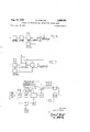
- Figure 1 represents a block diagram of the system.
- Figures 2 and 2a show certain wave forms and curves of units of the circuit.
- FIGS 3, 4, 5, 6 and 7 show units of the block diagram shown in Figure 1.
- Figure 8 shows a more complete block diagram than shown in Figure 1, illustrating more completely the elements following the recorder of Figure l.
- Figure 8a is a set of curves illustrating the transformations of the original signal and its recompositions in the type of modulations of the present invention.
- Figures 9 and 10 show respectively circuit diagrams to the recorder and from the recorder to the means wherein the reconstructed wave form is produced.
- FIG. 10a shows details of the signal sensing circuit.
- Figure 10b shows the selective triggering circuit and Figures 10c, 10d and 10e show curves relating to it.
- Figure 11 shows a multiplier gate circuit
- Figure l2 shows a feed back recorder detail.
- Figures 13, 13a and 13b show a wave form and modification of the circuit of Figure 1.
- the modulator circuit 3 transforms the input signal of 3 into a signal which changes abruptly from one mode to another, see Figure l2, such that successive time intervals defined by these abrupt changes ofmode bear the followman1-2 U tri-t2 where Y'r lies somewhere in the .interval tft-f2.
- the output signal of the modulator 3 is now fed through a pulse forming circuit 4.
- This circuit derives short sharply defined pulses from the output signal of 3, which as Was explained above, has abrupt changes between two modes.
- the pulses thusproduced at theoutput of 4 are now recorded on the magnetic tape of recorder 5.
- the method of recording is of secondaryy importance, although oneV should strive to utilize a method which is particularlyowell suited to record verynarrow V(in space dimension) pulses on the magnetic tape.
- the ratio of successive time intervals as bounded Y by the reproduced pulses is the same as Vduring the original recording, and this ratio defines the signal amplitude at aV time -Within the time interval in question.
- the remaining portion of the reproducing circuit is a device which actually synthesizes this ⁇ signal voltage by'utilizing the pulses from the output of theV recorder 5.
- Va pream-VV plifier is not incorporated in the recording device, or if lthe existing preamplifier docs not have suitable amplification characteristics for the purpose at hand (see further de-V tails below) it is generally necessary to precede the actual demodulator circuit 7 by ya suitable preamplifier circuit 6'. 'Y
- This amplifier must not of necessity be an electronic ami plifier.
- a pulseY transformer or similar device canV conceivably perform the same function.
- the preamplifier might'also be embodied into the vdemodulator circuitV 7 itself.
- Y Y Y f The demodulator circuit 7 now generates the original signal or'a functionfof the original signal such as a mul# tiple, a fraction, or the product of the' original signal with some other signal available at the time of reproduction, or a function (in the mathematical sense) of the original signal amplitude, making use of the time relationship betweenothe pulses delivered bythe preamplifier@ l.
- the demodulator Vcircuit will generally include a more or less elaborate filtercircuit to eliminate what -might be called the sampling noise? This sampling noisevhas a funda- Vmental frequency which is e'qual'to"1/2V the number of pulses per second at the output of the preamplifier 6.
- This modulation ratio might be defined as the ratio of the degree of modulation actually used over the degree of modulation conceivably (though not necessarily practically) possible.
- frequency modulation for example, the deviation in frequency from the center frequency (the actual degree of modulation) divided by the center fre;4
- Vquency (the conceivable degree of modulation) is rarely ever higher than a few percent.
- Vratio modulation wherein the actual degree of modulation measured by the ratio (t-t2)/ (t1-H2) can easily be made to range between -1/2 and 1/2, whereas the conceivable degree of modulation can only extend from l to 1, it is clear thatY the modulation ratio is of the order of 50%; In addition, it ispossible to demodulate linearly, without1any particular precautions, modulation ratios even as high as 70%. This stands'in clear contrast to frequency modulation, where theV characteristics of ordinarily used demodulator circuits are linear only in-a fairly-restricted range which forces one to Workwith a low modulation ratio if linearity is essential.
- the modulator using high ⁇ gain feedback circuits and fast acting flip-flop circuits is capable of an yaccuracy of the order ofr/oo of 11% depending onthe quality of the components used.
- the demodulator circuit consisting of the same kindof fast acting nip-flop circuits and high gain feedback circuits canbe made to have substantially'the same accuracy.
- the recording andV Y reproducing accuracy depends only on thenarrowness'of the recording gap Width'in relation to the separation o-f consecutive pulses on the tape.
- the Yerror which-might possibly be introduced by this can vbe shown tobe of the orderY of only 1/15 of one percent, in Ya Vtypical case vof aV rlow frequency signal recorder. Even so, the kind of error introduced is rather of the nature .ofra iiuctuating noise'than an actual non-linearityof reproduction. 'A carefullyrdesigned recording Yand'playback circuit arrange# ment might, therefore,rreproduce with an accuracy of better than one tenth of one percent.' Inifact,the simple .Y
- This low frequency noise now can either originate inthe electronic circuitry, such as the modulator or the demodulator, Vor it 'can originaterfroin wow and iiutter-modulation of the pulse ⁇ stream picked upY by the playback head.
- the iirst'kind of low frequencynoisefcan beY reduced Yto a verylow level byV careful design of the electronic cire "cuits in question; ⁇ Except for fdrift(which"coul ⁇ d be eliminated by known methods), the low frequency noise caused by these circuits alone Vwas found V,to be completely unimportant ⁇ in the Yexperimental circuit built.Y
- Another useful feature of the recorder is that it is possible with the addition of but a simple circuit to multiply immediately electronically the output signal with some other signal which is available at the time of reproduction. This is so, because one only has to replace the unityvoltage delivered to the demodulator as a measure from which the final signal output is constructed, by any other suitable voltage source which may be time variant.
- the demodulator circuit in this arrangement has some similiarity to other circuits like the electronic multiplier used in analog computing. However, there are important differences, especially in regard to the pulse frequency, the ltersused, and especially in the basic application of pulse time ratio modulation which is impor- .tant in the present invention.
- pulsetime ratio modulation is primarily use'd to be able to record with unusually high accuracy a given signal of relatively low frequency.
- the problem of delay is of secondary importance since the recorded signal is played back delayed anyhow.
- This allows the use of much lower pulse rates than those encountered in electronic multiplication. This in turn necessitates changes from the circuit arrangement used in several electronic multipliers. While the possibility of electronic multiplication is mentioned mainly to point out the versatility of this recording method in comparison to other schemes, nevertheless the special types of multiplier circuits designed ⁇ to overcome the specific diiculties encountered with these necessarily low pulse rates are believed to be novel and highly important for applications of this recorder to a large group of problems.
- the means of converting signal into voltage wave of suitable amplitude (circuit 2 of Figure l) is exemplified as an operational amplifier, similar to the ones used in electronic analog computers, if the signal itself is already a voltage wave.
- a high accuracy recorder deserves high accuracy intermediate components such as in this instance.
- A is a high gain D.C. amplifier with a feedback resistor R2 and an input resistor R1.
- the ratio Rg/Rl is the actual amplification of the entire unit. This can easily be adjusted to be any reasonable amount. Ordinarily, the highest accuracy will be obtained without undue complications if the input signal amplitude range--if it is already a voltage wave as assumed here--is anywhere from about one volt to several hundred volts. If unity voltage is 100 voltsas will be assumed in this example case-then it is advisable for maximum utilization of accuracy and signal to noise ratio, to arrange that the output of circuit 2 of Figure 1 is also ranging between -100 and +100 volts.
- FIG 4 illustrates one possible circuit arrangement for circuit 3 of Figure 1.
- the input of the summerintegrator I is supplied through R1 with the input voltage which shall be called X, and through R2 with a voltage derived from the flip-flop circuit, F.F.
- This voltage from the output of the iiip-tiop, F.F. is either very closely volts or very closely -100 volts, depending on the mode that the bistable ip-iiop is in.
- the mode of the flip-flop is controlled by the output of the integrator I in such a fashion that if the integrator output should become as low as a certain critical voltageUl (see Figure 2a), then the ip-iiop output will change to -100 volts.
- T2ST2 S T3 f2 is value between adjacent numbered T (see above).
- Tifi'rsrz'ra 'r3 is value between adjacent numbered t (see above) l time interval trl-t2.
- the modulator may be looked upon as a means by which the voltage wave is Ycontinuously sampled a greatmany times ⁇ a second in such a way that the ratio of the times between suc- Y cessive pulses is a function of the signal amplitude, Such continuous sampling provides pulse time ratios at successive increments which are functions ofthe voltage wave.
- FIG. 13a A different method for obtaining pulse time ratio modulation is shown in Figure 13a.
- a sawtoot generator produces waves of a triangular shape. Theupward and downward slopes of this sawtooth wave must not of necessity be equal, but the average voltage of the sawtooth wave should be zero.
- Y A .typical such sawtooth Wave is shown in Figure 13.
- Thersignal wave X is now added to the sawtooth wave in the summer Su of Figure 13a. The resulting wave is no longer centered laround Zero volts as was the case with the wave of Figure 13. Instead, lthe time intervals t1 and t2 during which the output wave of the summer is below and above zero volts respectively bear the following relation to the signal voltage X (if X is constant):
- V I Y a The sawtooth method for obtaining pulse timev ratio modulation simplifies multichannel recording because the same sawtooth wave may be used Von all channels.
- the summer and limiter may be combined into one circuit of relatively simple construction.y
- YMultiplex recording may be obtained by the use of coders. 'E.g., a two channel multiplex recording systemV usinggthe sawtooth method is shown in Figure 13b."
- the pulse time ratio modulated square Vvvayes arecodedY and then mixed in the mixer. Coding'isVY essential because theV mixed signals ⁇ must be separated on playback.
- v -E.g., cod-f ing may consist fof amplitude modulatinga sinusoidal carrier bythe square Wave emerging from the outputvof the limiter amplifier, using diierent carrier Yfrequencies for different channels. No crucial accuracy is required in these coders.
- the output Vof -the mixer-circuit is recorded. On playback, the reproduced signal.
- decoder circuits for each channel, whichV select the respective pulse-timeratio modulated signal'from the mixed signal atthe output of the recorder.
- the decoder should bea Vband pass lter withthe carrier frequency of the respective channel lying in the, center ofthe pass band, the pass band being ⁇ as wide as possible without causing interference Vwith other channels.
- channel has a demodulator which synthesizes the original signal at its output.
- Vthe Voutput of Att. is passed through a cathode follower C.F. YNow, thesliarply deiinedpulses are derived from the output of C.F.fby a suitable R-Cdiierentiator circuit.V VThe time constant should be adjusted to yield the desired shortness ofthe lt is also possible to deliver the output of the circuit in Figure 5 directly to the magneticrecord-- ing'head. ⁇ In that instance, the Vimpedance of the recording head has Vto be considered in determining the time Y,
- Vit might be. more desirableY leaveout circuit 4 of Figure 1 and recordvthe Youtput yof circuit 3 of Figure 1 directly.. Y
- This average voltage is seen to be equal to the voltage 1z (f3) which existed at some intermediate time f5, in the time interval under consideration.
- a very high noisevoltage of 200 volts peak-to-peak magnitude is still superimposed on this desirable signal voltage.
- This seems very high--the noise is actually always bigger than the signal-one can nevertheless always reduce this noise to a level below IAO@ of one volt without affecting the signal, because .the noise voltage consists of frequencies considerably higher than the signal frequencies.
- This filter circuit F1 needs special consideration, because it has to have fairly sharp cut-off characteristics, and at the same time be as nearly free from overshoot and losses as possible.
- a lowpass filter built from L-C sections will be adequate. For extremely low cut-off frequencies one is better off using R-C filters whose characteristics are corrected by a suitable feedback loop from the output of the separating-amplifier A.
- the L-C filter however is restricted to use with a reasonably high cutoff frequency of at least a few cycles per second.
- the output of the filter is then passed through lone final amplifier whose main purpose it is to make the signal available at essentially zero ohms output impedance.
- Figure 6 shows another circuit S.S.,which could be called signal senser.
- S.S. which could be called signal senser.
- This addition was found necessary to eliminate the annoyance caused by the fact that without any pulses delivered to the flip-Hop e.g. when the tape was not moving, the liip-op would remain at either -l-lOOor -100 volts.
- the output voltage of the demodulator was highly positive or negative beyond the limits that the signal voltage could ever reach. This was found to be undesirable in certain analog computer applications. In fact,V one desired zero voltage output for the no-signal condition.
- the output signal of M is treated in exactly the .same manner as the output signal of the iiip-iiop in Figure 6.
- Modulator Chenin- Figure 8 gives a block diagram of the circuit which is given in all details in Figures 9 and 10.
- curve (l) represents a signal which is desired to be recorded, which may be a periodic or aperiodic signal.
- Curve (2) is a wave form derived from curve (l) by the applications of pulse time ratio modulation and is the continuous sampling wave at the output of the multivibrator of the modulator ( Figure 4), circuit 3, ( Figure l) and d Figure 8.
- Curve (3) shows enlarged portions of curve (2).
- Ourve (4) indicates the current pulses applied Ito the recording head corresponding to the elements of curve (3), see e of Figure 8.
- Curve (5) shows the pulses of curve (4) when played back, see f of Figure 8.
- Curve (6) shows the triggering portion of the pulses of curve (5) which cor responds to the points on curve (2) where the modes abruptly change indicating the sharpness and accuracy of location of the reversals in curve (2).
- the output of the multivibrator of the demodulator circuit '7 ( Figure l) and Figures 8 and l0 looks on play back like curve (2).
- the average voltage of curve (2) which is obtained by passing the wave of curve (2) through a low pass lter is then the original signal shown in curve (l).
- the integrator l, Figure 9 consists of tubes T1a and T15, T29, and T25, and T3.
- the diiferent gain inputs xl., x4, and x20 are effected by suitable input resistors R1 to R3.
- the integrating capacitor is C2.
- Appropriate controls R5 to R5 in the D.C. amplier portion of the integrator allow respectively adjustment of zero, balance, and compensation C1 and R23 suppress oscillations of the high gain feedback amplifier of I. ln
- the integrator has no automatic balancing control. Such a circuit, however, could easily be added to the integrator.
- the liip-fiop consists of Tubes T4, T55 and T53, and T5.
- T55, and T55 called as a unit T5
- T5 may be a single tube forming a bistable multivibrator.
- the tiring of this multivibrator is controlled by the integrator over the resistor R27.
- the swing of the integrator output voltage is approximately 200 volts.
- T4 and T6 control the plate voltages of the two sections of T5 to be either or -100 volts. Any error caused by the nonzero forward resistance of these diodes T5,l and T51, (which usually results in a constant error in the final output voltage) can be eliminated with the zero adjustment, las'long as the error is consistant which is usually ythe case.
- the output of the flip-hop is fed back over R34 to the grid of the integrator input tube T1. It also feeds over the divider R35', R38 to the grid of the cathode follower T7,
- the output of the VcathodeV follower feeds through the diierentiator C3R39 to the recording head.
- T8a and T81 are the erase oscillator tubes. put of the oscillator feeds to the erase head. v
- the relay, Ry, Figure 9 is ordinarily controlled by a switch, S1. However, foruapplications in automaticcomputing, the relay can also be controlled by a suitable relay amplifier of the computer.
- Demodulator circuit (Fig. 10).--The first part of the demodulator circuit is a two-stage amplifier with a total' gain of approximately 1000.
- the coupling networks have a fairly short time constant of the order of a millisecond.
- the magnetization pulse is now differentiated since the output voltage of the playback head depends on the rate of VchangeY of flux in theV gap. The steepest portion of this is seen from the figure to lie in the middle of the N-shap-ed pulse curve f or as indicated more fully Vin curve (6) of Figure 8a. This portion of the pulse is then used to re the ilip-ilop of the demodulator.
- the selective tnggering circuit acts as a pulse filter ( Figure 6) land consists of two'diodes Tim and vTCH, whose plates are connected to the grids of the two triodes '1"'5a and T5b comprising a regular bistable multivibrator.
- the diodecathodes are biased from resistance dividers R'17 and R'15, and Rm and Rm connected from the plates of the triodes to the minus potential as shown in Figures l and 10b.
- the resistance dividers are chosen in such a way that the cathode potential of the diode which is next to the saturated triode is slightly positive-by'an amount Ae.
- Ae should be appreciably larger than the/expected noise voltage .in the trigger pulse stream and should be much less than the magnitude or" the peak-to-peak trigger pulse voltage. through two capacitors C4 and C'5 connected to the diode cathodes.
- each triggering pulse tp appears attenuated at the diode cathode due to the smallness of the time constant RC compared with the rise time of ,these portions.v Y Y Byvvpro-per choice of component' values, it canbe arranged that the attenuation is so great that the resulting Voltage at the diode cathode is less than Ae and, therefore, always insuicientffor triggering.
- the steep middle portion,A whichrpassesrthrough toV the vdiode cathodejalmost unattenuated' is capable of .triggering the iiip-op.
- Typical ⁇ wave shapes r.at thecathode and the plate ⁇ of a diode are-shown in Figures v10a? and 10c respectively.
- T', and Tq again limit vthe plate voltages of the flipop to '4i-.10,0 and -100 volts.
- the plate voltage atrT5b is now Ythe sameas. the plate voltage that existed at T'5b of the modulator circuit during frecord.
- This signal is then passed through a foursection, R'25 to R29 and Ca Cn R-C lter t0 the input Of Tgc aridTAgb. Tga. and TSb VT'm, Vand Tgb, and Tmcomprise the separating amplier.
- the feedback consists of a D.C. path to adjust the desired gain andan A.C.
- the frequency response was flat to 0.1 cycle Y per second, wasV fiat within 1% to slightly beyond one cycle perv second,V 'then'dropped off very sharply to a negligible amount beyondl ten cycle per second.
- the D.C. gain can be cihosen either x or acl/10.
- the coarse and fine balance adjustment of the output )amplifier is effected by R32 and R31 respectively.
- The-signal senser circuit consists of atube Tu withV a relay-Ry in Ythe plate circuit.
- the grid is connected to B-lbythe large resistor'RGZ so as to cause a current ow through it of magnitude' eB/R where R is the value in ohms of this resistance.
- the multiplier consists of '8 diodes D1 to D8 inclusive arranged as shown in'V Figure V11.
- the inputleads are of sufiicient voltage.
- the time ratio modulation is obtained from an original signal X.
- Another signal voltage Y, intended to multiply X is supplied push-pull to the leads marked Y and -Y.
- the capacitors and re sistors connected to each diode branch effect an equalization of the diode currents independent of the magnitude or sign of Y. It can be seen that the output lead is either at Y volts or -Y volts, depending on the mode of the time-ratio modulated input square wave. The average value of this output voltage, averaged over Ione complete cycle is, therefore,
- the accuracy and frequency response of the modulator and demodulator circuit may be improved if a reasonable amount of feedback is applied as shown in Figure 12.
- the demodulator is connected directly to the modulator output by means of a switch, yielding a voltage -X at the domodulator output.
- X Will be approximately equal to X.
- This feedback arrangement is not restricted in its usefullness to time ratio modulation recording, but is applicableV in all recording schemes where the recording mechanism, the recording heads and the magnetic tape do not introduce any appreciable error.
- a method of recording and reproducing electrical waves which comprises continuously sampling the waves at a rate at least twice as great as the highest signal frequency component desired to be reproduced, producing by the sampled increments abrupt changing voltage modes such that successive time intervals defined by these abrupt changes of mode bear the following functional relation to the input signal wherein U is unity voltage, an arbitrary voltage used as a reference, X is the voltage of the input and t1 and t2 define successive time intervals where the mode changes, then producing thereby short sharply defined pulses at points of said abrupt changes, magnetically recording said pulses, and thereafter reproducing said recording and synthesizing the original signal.
- a method of recording and reproducing electrical Waves which comprises continuously sampling the waves, producing by the sampled increments abrupt changing voltage modes such that successive time intervals defined by these abrupt changes of mode bear the following functional relation to the input signal U rl-tz wherein U is unity voltage, an arbitrary voltage used as ne successive time intervals where the mode changes, then continuously magnetically recording said abrupt changes yand thereafter reproducing said recording and synthesizing the desired function of the original signal.
- a method of recording and reproducing electrical waves which comprises continuously sampling the waves
- the method of recording and reproducing electrical Waves which comprises continuously sampling the signal wave, producing by the sampled increments abrupt changing voltage modes such that successive time intervals defined by these abrupt changes of mode bear the following functional relation to the input signal U a+a wherein U is unity voltage, an arbitrary voltage used as a reference, X is the voltage of the input and t1 and t2 define successive time intervals where the mode changes, then producing thereby short sharply defined pulses at points of 'said abrupt changes, magnetically recording said pulses, thereafter reproducing said recorded signal, demodulating the same including liltering and producing a synthesized signal as a function of the original signal. 5.
- the method of recording and reproducing electrical waves which comprises continuously sampling the signal wave a large number of times per cycle and converting the 'same into sharp' pulses such that the ratio of the difference to the sum of successive time intervals between pulses is a function of the input signal and magnetically recording the pulses so produced.
- the methodV of producing a product of two electrical Waves occurring at different time positions which comprises continuously sampling the' earlier occurring electrical Wave a large number of times per cycle and converting the same into sharp pulses such that the ratio of the difference to the sum of successive time intervals between pulses is a function of the input signal, magnetically recording the pulses so produced, reproducing the pulses at the time of the occurrence of the second wave, converting said pulses to corresponding square topped waves and multiplying the same in an electrical mixing circuit.
- the method of producing a product of two electrical waves occurring at different time positions which comprises continuously sampling the earlier occurring electrical wave converting the same into a pulse-time-ratio modulated square wave, recording the same, reproducing the same at the time of the occurrence of the second wave and multiplying said squared wave with said second wave and thereafter filtering the product of the squared wave and the second wave in order to obtain the output of the first and second wave.
- a system for recording a signal Wave comprising means for modulating opposite substantially square topped Wave modes with the signal Wave such that successive wave mode changes establish time ratios as a function of the signal Wave, means for converting the output of said modulating means to corresponding sharp pulse Waves, means for recording said sharp pulse Waves as a source Vfor synthesizing the original Wave and demodulator means responsiveronly to the ratio of times defined by said successive pulse Waves.
- a system for recordinga signal Wave comprising meansV for modulatingV opposite substantially square topped wave modes with the signal wave such that successive Wavermode changes establish time ratios as a Y function of the signal Wave, means for recording the modulated modes as a source for synthesizing the original signal anddemodulator means responsive only to the ratio of successive modes.
- a system for recording a signal wave comprising an amplier having a controlled output', electrical circuit means, an integratorY connected to the output'of the am-V plifier and the output of said electrical circuit meansY for integrating both the signal received from the am-V plier and another signal fed back from said electrical circuit means, said electrical circuit means providing two square topped opposing wave modes adapted to change abruptly from one to -another dependent upon the input signal impressed thereon, the input of said circuit means connected to the output of said integrator, a recorder,
- a system for producing pulse-time-ratio modulation comprising a signal input means, an electric integrator circuit connected to said input means, a bi-stable electric multivibrator circuit connected to the integrator circuit' and controlled thereby with said multi-Vibrator having an output, means connecting the output of said multivibrator circuit in feed back relation to the input of the integrator, said connecting means including means for combining the output of the multivibrator with the signal input to establishinstalle time ratio modulation and means providing an output of the system through which saidV back signal of said circuit means, the input o-f said circuit means connected to the output of said integrator, an attenuator connected to said circuit means, a cathode follower connected to said attenuator and a recorder operatively connected to said cathodefollower.
- a system for recording and reproducing arsignal wave which comprises means for modulating opposite substantially square topped wave modes with the signal wave such that successive mode .changes establish time ratios 'as a Vfunction of the signal Wave, means for converting the outputof said modulating means to correspending sharp pulse Waves, means for recording said sharp pulse waves as a source Yfor synthesizing the original Wave, in combination Withrmeans for synthesizing said signal comprising a Ydemodulator operatively connected lto said recorder forproducing from impressed sharp pulse waves square wave formshaving opposing modes, a filter and separating amplifier connected in cascade with said demodulator.
Description
H. B. BEI-CK Filed Aug. 26, 1955 e sheets-shave@ 1 5/ 6AM L CON v5? Tie M aow/:T02 PULSE ranM/N@ SOURCE cmT MA 6/1/5 T/c l REcaqoc-:R
z j 6 s..
` PREAMpL/F/Ez gMapz/@A Tae l F02 PUASES FIG." E
FIG 1 Emu.;
HG. A
1N V EN TOR.
Aug. 23, 1960 H. B. BELCK 'i 2,950,352A
SYSTEM Foa RECORDING AND REPRoDucING SIGNAL wAvEs A Filed Aug. 26. 1953 e sheets-sheet 2 HQE S/GWA L 5 EH56@ y VMM FIG 7 ,756020.56110 l PLAyA cl HEAD 55/v55 I ERA se HEAD IN VEN TOR. im Mw e/c/ Aug. 23, 1960 H. B. BELK SYSTEM FOR RECORDING AND REFRODUCING SIGNAL WAVES Filed Aug. 26. 1953 6 Sheets-Sheet 3A Vivir-mmh VII-IV Osc/Larme cmpmsa nav Aug 23 1960 H. B. BELCK 2,950,352
SYSTEM FOR RECORDING AND REPRODUCINQ SIGNAL wAvEs Filed Aug. 26, 195s s sheets-sheet 4 AUSL 23, 1960 H. B. BELcK 2,950,352
SYSTEM FOR RECORDING AND REPRODUCING SIGNAL WAVES Filed Aug. 26, 1953 6 Sheets-Sheet 5 e8 RELAY .EA/526mg@ I e QELAy @Femm-Eo a/v/.y Wye-V ca/vT//vaaus c. cumeEA/v- F/vws Tn P o zero VOLTAGE AT /ocom//nj G12/p Eg ffm ff fm Fl@ 10A L64 /g /a'f H D-Q--- 7,55 .JUm [13 if if A52/edm@ 'ef/w00' c//fz//z @000 IN VEN TOR. Hans e/c/ Aug. 23, 1960 H. B. BELCK 2,950,352
sysTx-:N Fox RECORDING AND REPRoDucING SIGNAL wAvEs Filed Aug. 26, 1953 6 Sheets-Sheet 6 A Mp4 /F/ER SYSTEM FOR RECORDiNG AND REPRODUCNG SIGNAL WAVES Hans B. Belek, Troy, NX., assigner to Rensselaer Polytechnic Institute, Troy, NX., a corporation of New York Filed Aug. 26, 1953, Ser. No. 376,689
Ciaims. (Cl. 179-1002.)
The present invention relates to recording and reproducing signal waves, more particularly to recording and reproducing in which a magnetic tape recorder may be used to record signals containing frequencies from zero or D.C. to several thousand cycles per second with an unusual accuracy up to about one-tenth of one percent full scale. Some typical applications of the present invention are in the following fields:
Any kind of low frequency analog computing.
Recording of seismic signals.
Recording of brain waves and related applications in the medical and physiological held.
In the prior art of magnetic recording, the following means have been used:
(u) Amplitude modulation-This allows the recording of higher frequencies but is much too inaccurate for the applications contemplated, e.g. in conjunction with electronic analog computers. It also lacks the possibility of recording D.C. signals and signals of extremely low frequencies of the order of tenths of cycles per second.
(b) Frequency modulation- Although the accuracy of frequency modulation is better than in amplitude modulation and although D.C. signals can be recorded, the achieved accuracy of about one percent full scale is still insuticient for applications in the high accuracy analog computor eld. In addition, the zero level of the reproduced signal depends critically on the center frequency of the demodulator circuit and on the tape speed. Ref sulting errors can be eliminated only by the use of elaborate compensation circuits.
(c) Pulse width modulation and pulshez'ght modulation-Pulse height modulation has shortcomings similar to those of amplitude modulation although to a lesser degree. Similarly, pulse width modulation has disadvantages similar to those encountered in frequency modulatlon.
(d) Pulse code modulation-This is perhaps the most accurate existing method of recording signals. However, the circuits necessary for a pulse code modulated recorder are complicated and costly. In spite of that, the accuracy attainable with a pulse code type recorder is still limited to the accuracy of the necessary analog-todigital and digital-to-analog converters which will hardly exceed the order of one-tenth of a percent full scale.
Advantages of invention The method of recording which is the content of this inveniton is to use what might becalled pulse time ratio modulation. The signal to be recorded is first converted into a succession of sharply dened pulses such that the ratio of the times between two successive pulses is a function of the signal amplitude. These sharp pulses are then recorded on magnetic tape. Ifthe magnetic tape is played back, the same series of pulses is obtained and the original signal can be constructed from these pulses. The following advantages result from this method of recording:
The accuracy is unusually high, because the informa- Patented Aug. 23, litri@ tion recorded is nothing but the relative location of sharp pulses on the tape. This information is highly independent of the recording characteristics of the magnetic tape, the magnetic recording head and any preamplifiers used. Moreover, since only the ratio of successive intervals determines the signal strength, the amplitude of the reproduction is independent of the playback speed over a very large range. This eliminates the necessity of elaborate speed controls in many applications. tIt results in a high signal to noise ratio. Noise caused by flutter and wow is very low, such that inexpensive recording mechanisms will yield essentially the same high accuracy. .Additionally, a signal can be recorded at one speend and played back immediately without any readjustments at an entirely .different speed up to many times faster or slower than the speed of recording. Another feature consists of the possibility to electronically multiply the output signal of the recorder with lany other suiiiciently slowly varying signal with a degree of accuracy of the same order. Only a small amount of additional circuitry is required for this multiplication. This feature is very important in the application of this recorder for statistical analysis, Fourier analysis, expansion of arbitrary functions in a series of orthogonal functions, solution of non-linear, ordinary and partial differential equations.
The combined features of this recorder allow a new approach to the solution of partial differential equations on electronic analog computers such as` the REAC which ordinarily can be used only for the solution of ordinary differential equations. In contrast to existing special purpose analog computers for the solution of partial differential equations, the achieved accuracy and the diversity of problems solvable by this method is very high.
Other andv further advantages of the present invention will be best understood from the description of the invention in the specification set forth below when taken in connection with the drawing illustrating an emobdiment thereof, in which:
Figure 1 represents a block diagram of the system.
Figures 2 and 2a show certain wave forms and curves of units of the circuit.
Figures 3, 4, 5, 6 and 7 show units of the block diagram shown in Figure 1.
Figure 8 shows a more complete block diagram than shown in Figure 1, illustrating more completely the elements following the recorder of Figure l.
Figure 8a is a set of curves illustrating the transformations of the original signal and its recompositions in the type of modulations of the present invention.
Figures 9 and 10 show respectively circuit diagrams to the recorder and from the recorder to the means wherein the reconstructed wave form is produced.
Figure 10a shows details of the signal sensing circuit.
Figure 10b shows the selective triggering circuit and Figures 10c, 10d and 10e show curves relating to it.
Figure 11 shows a multiplier gate circuit.
Figure l2 shows a feed back recorder detail.
Figures 13, 13a and 13b show a wave form and modification of the circuit of Figure 1.
General description of 'invention The output of the signal source l, Figure l, is modified by some converter or transducer 2 into a voltage wave of suitable amplitude for the modulator circuit 3 which follows 2. In most instances, the signal from the signal source 1 will already be in the form of a voltage wave. Then 2 would be either an amplifier or an attenuator. `It is also possible to incorporate 2 in the modulator circuit 3 as will be illustrated.
The modulator circuit 3 transforms the input signal of 3 into a signal which changes abruptly from one mode to another, see Figure l2, such that successive time intervals defined by these abrupt changes ofmode bear the followman1-2 U tri-t2 where Y'r lies somewhere in the .interval tft-f2.
The output signal of the modulator 3 is now fed through a pulse forming circuit 4. This circuit derives short sharply defined pulses from the output signal of 3, which as Was explained above, has abrupt changes between two modes.
The pulses thusproduced at theoutput of 4 are now recorded on the magnetic tape of recorder 5. The method of recording is of secondaryy importance, although oneV should strive to utilize a method which is particularlyowell suited to record verynarrow V(in space dimension) pulses on the magnetic tape. Y
In some applications, e.g. recording signals containing 4 Y purposes such as immediate high-accuracy electronic multiplication. If one tries to evaluate the accuracy of a recording system, one Vwill be led to the conclusion that the obtainable accuracy`dependsV on the modulation ratio.
frequency components of several Vthousand cycles per -V second, it might be advantageous to dispense with the Y existed at the input of 3 during the recording process, one
plays back the magnetic record of the pulses. This play? back may take place at the original tape speed, or at a speedhigher or'lower thanthe original speed. In any event, the ratio of successive time intervals as bounded Y by the reproduced pulses is the same as Vduring the original recording, and this ratio defines the signal amplitude at aV time -Within the time interval in question. The remaining portion of the reproducing circuit is a device which actually synthesizes this `signal voltage by'utilizing the pulses from the output of theV recorder 5.' If Va pream-VV plifier is not incorporated in the recording device, or if lthe existing preamplifier docs not have suitable amplification characteristics for the purpose at hand (see further de-V tails below) it is generally necessary to precede the actual demodulator circuit 7 by ya suitable preamplifier circuit 6'. 'Y
This amplifier must not of necessity be an electronic ami plifier. A pulseY transformer or similar device canV conceivably perform the same function. The preamplifier might'also be embodied into the vdemodulator circuitV 7 itself. Y Y Y f The demodulator circuit 7 now generates the original signal or'a functionfof the original signal such as a mul# tiple, a fraction, or the product of the' original signal with some other signal available at the time of reproduction, or a function (in the mathematical sense) of the original signal amplitude, making use of the time relationship betweenothe pulses delivered bythe preamplifier@ l. The demodulator Vcircuit will generally include a more or less elaborate filtercircuit to eliminate what -might be called the sampling noise? This sampling noisevhas a funda- Vmental frequency which is e'qual'to"1/2V the number of pulses per second at the output of the preamplifier 6.
This modulation ratio might be defined as the ratio of the degree of modulation actually used over the degree of modulation conceivably (though not necessarily practically) possible. In frequency modulation, for example, the deviation in frequency from the center frequency (the actual degree of modulation) divided by the center fre;4
Vquency (the conceivable degree of modulation) is rarely ever higher than a few percent. In this pulse time Vratio modulation, wherein the actual degree of modulation measured by the ratio (t-t2)/ (t1-H2) can easily be made to range between -1/2 and 1/2, whereas the conceivable degree of modulation can only extend from l to 1, it is clear thatY the modulation ratio is of the order of 50%; In addition, it ispossible to demodulate linearly, without1any particular precautions, modulation ratios even as high as 70%. This stands'in clear contrast to frequency modulation, where theV characteristics of ordinarily used demodulator circuits are linear only in-a fairly-restricted range which forces one to Workwith a low modulation ratio if linearity is essential. i
A simple calculation now suffices to estimate the 'possible accuracy of the method in a particular model actually built: The modulator, using high `gain feedback circuits and fast acting flip-flop circuits is capable of an yaccuracy of the order ofr/oo of 11% depending onthe quality of the components used. Similarly, the demodulator circuit consisting of the same kindof fast acting nip-flop circuits and high gain feedback circuits canbe made to have substantially'the same accuracy. The recording andV Y reproducing accuracydepends only on thenarrowness'of the recording gap Width'in relation to the separation o-f consecutive pulses on the tape. The Yerror which-might possibly be introduced by this can vbe shown tobe of the orderY of only 1/15 of one percent, in Ya Vtypical case vof aV rlow frequency signal recorder. Even so, the kind of error introduced is rather of the nature .ofra iiuctuating noise'than an actual non-linearityof reproduction. 'A carefullyrdesigned recording Yand'playback circuit arrange# ment might, therefore,rreproduce with an accuracy of better than one tenth of one percent.' Inifact,the simple .Y
model built, for` the -pur-poseof Ylaboratory testing, which can be said to use only components of averagequali'ty, and especially in regard to the vrecording mechanism utilized a machineof the most inexpensive popular` dee- Y sign, even this simple moidelexhibite'dan accuracy, sta'- bility, Vand linearity definitely Within if or-JA'O of one percent. Y Y o The signal 'toY noise ratio can Ybe Vshown to be high for i the following'reasons: Any high frequency'components of the noise v-whichexist at the output of the demodulator will be completely eliminated by the filters included in the demodulator circuit7. The'only kindof objectionable noise would, therefore, be of a low frequency. This low frequency noise now can either originate inthe electronic circuitry, such as the modulator or the demodulator, Vor it 'can originaterfroin wow and iiutter-modulation of the pulse `stream picked upY by the playback head. The iirst'kind of low frequencynoisefcan beY reduced Yto a verylow level byV careful design of the electronic cire "cuits in question;` Except for fdrift(which"coul`d be eliminated by known methods), the low frequency noise caused by these circuits alone Vwas found V,to be completely unimportant `in the Yexperimental circuit built.Y
The only detectable Vlow frequency'noise originated from the abovementioned- Wow and `flutter modulation,butY it was possible to reduce the noise to avleyel of lower Aonly vlow frequency icon rponnts .ofY the taperjspeed, variaabove, and since naturally the low frequency' acceleration magnitude will be very small for any mechanism which is acceptable for but the lowest demands on quality, it follows that ordinarily wow and utterrmodulation will be of negligible importance. A qualitative mathematical analysis shows just this behavior and this analysis is supported by actual tests with mechanisms wherein the Wow and flutter is artificially produced and controlled.
Another useful feature of the recorder is that it is possible with the addition of but a simple circuit to multiply immediately electronically the output signal with some other signal which is available at the time of reproduction. This is so, because one only has to replace the unityvoltage delivered to the demodulator as a measure from which the final signal output is constructed, by any other suitable voltage source which may be time variant. The demodulator circuit in this arrangement has some similiarity to other circuits like the electronic multiplier used in analog computing. However, there are important differences, especially in regard to the pulse frequency, the ltersused, and especially in the basic application of pulse time ratio modulation which is impor- .tant in the present invention. In this invention pulsetime ratio modulation is primarily use'd to be able to record with unusually high accuracy a given signal of relatively low frequency. The problem of delay is of secondary importance since the recorded signal is played back delayed anyhow. This allows the use of much lower pulse rates than those encountered in electronic multiplication. This in turn necessitates changes from the circuit arrangement used in several electronic multipliers. While the possibility of electronic multiplication is mentioned mainly to point out the versatility of this recording method in comparison to other schemes, nevertheless the special types of multiplier circuits designed `to overcome the specific diiculties encountered with these necessarily low pulse rates are believed to be novel and highly important for applications of this recorder to a large group of problems.
Description of invention in ntrmedz'ate terms This section is presented partly to give a more direct and detailed picture as a further illustration to the general description given above, and partly as a fairly detailed block diagram for an actual circuit which has been built primarily for laboratory tests and which will be described in all details below. In this section circuit arrangements are usually given their generic terms such as amplifier, integrator etc., if such circuits are considered to be generally known, and if the functioning of the entire circuit does not to a considerable extent depend on the particular realization of these .operational circuits.
In Figure 3, the means of converting signal into voltage wave of suitable amplitude (circuit 2 of Figure l) is exemplified as an operational amplifier, similar to the ones used in electronic analog computers, if the signal itself is already a voltage wave. A high accuracy recorder deserves high accuracy intermediate components such as in this instance. A is a high gain D.C. amplifier with a feedback resistor R2 and an input resistor R1. The ratio Rg/Rl is the actual amplification of the entire unit. This can easily be adjusted to be any reasonable amount. Ordinarily, the highest accuracy will be obtained without undue complications if the input signal amplitude range--if it is already a voltage wave as assumed here--is anywhere from about one volt to several hundred volts. If unity voltage is 100 voltsas will be assumed in this example case-then it is advisable for maximum utilization of accuracy and signal to noise ratio, to arrange that the output of circuit 2 of Figure 1 is also ranging between -100 and +100 volts.
Figure 4 illustrates one possible circuit arrangement for circuit 3 of Figure 1. The input of the summerintegrator I is supplied through R1 with the input voltage which shall be called X, and through R2 with a voltage derived from the flip-flop circuit, F.F. This voltage from the output of the iiip-tiop, F.F., is either very closely volts or very closely -100 volts, depending on the mode that the bistable ip-iiop is in. Now, the mode of the flip-flop is controlled by the output of the integrator I in such a fashion that if the integrator output should become as low as a certain critical voltageUl (see Figure 2a), then the ip-iiop output will change to -100 volts. If the integrator output should reach a certain otherV critical voltage U2 U1, then the iiip-op output voltage will change to +100 volts. The behavior of the circuit of Figure 4 can now be understood with the aid of Figures 2 and 2a. Assuming that the integrator output has just been at a voltage level U1 and thereby caused the output of the flip-flop to be -100 volts the combined input current to the integrator will then be ,-l00/R2+X/R1. It is necessary that this quantity benegative for all allowable values of X. If X is limited to values between -100 volts and +100 volts then a resistance ratio R2/R1 of 1/2 will automatically assure this necessary relation. Such a resistance ratio will correspond to a modulation ratio of 50%.
Since now the combined input current to the integrator is negative, the output voltage rises as follows (see Figure 2a):
Ue):UlJfaloo-xoiht v (i) where oc is the rate of integration of the integrator, Rg/Rl is assumed to be 1/2.
Y The output voltage will continue to rise until it reaches the critical value U2. At this instant, the flip-flop suddenly changes its state and offers now a voltage of +100 volts to the integrator input. This not only puts a stop to the rise of the integrator output voltage but actually effects a decay of this voltage. The relation for the decay of the integrator output voltage is:
`The integrator output voltage continues to drop, until the critical level U1 is reached again. From then on, the integrator output voltage will rise again as before. Now, the following relations exist:
From
T1 Sri S T2 n 1s value between adjacent numbered T (see above).
From
T2ST2 S T3 f2 is value between adjacent numbered T (see above).
Hence from (1*) and (2*):
Tifi'rsrz'ra 'r3 is value between adjacent numbered t (see above) l time interval trl-t2.
(T37) interior to the interval under consideration is a function of the ratio Vlil/t2. It is also seen that this ratiofis independent of the rate of integration a, as wellas U1.
and U2. Of course-variationsV with time of these parameters wouldV cause a Vchangeeven inthe times ratio `t1/t2, but the change Aof times ratio t2/t1 depends only Yon the speed of these variations.V The'variation speeds of these parameters with time encountered inpractice are so. small that in this application these variationstare of no objectionn able consequence whatever. A simple calculation'can be made to show that this'behavir can'b'e predicted from theory. a v Y l At. this point is should be emphasized which factors will determine the ultimate accuracy ofthe modulator. These are: drift-rate ofthe integrator',raccuracy and stability ot' the ratio R1/R2,'stability of the outputlevels of the flip-flop. It can be seen, therefore, that the a6- curacy will not depend on the amount of drift of the integrator itself, but rather onrthe amount of rate of Ychange of drift of the integrator. This veryV definitely alleviates.
the problem of drift-control for the integrator. In' the same way, it is not necessary to have exactly +100 and 100 volts output levels of the flip-Hop, just as long as these values will not change with time. The modulator may be looked upon as a means by which the voltage wave is Ycontinuously sampled a greatmany times `a second in such a way that the ratio of the times between suc- Y cessive pulses is a function of the signal amplitude, Such continuous sampling provides pulse time ratios at successive increments which are functions ofthe voltage wave.
A different method for obtaining pulse time ratio modulation is shown in Figure 13a. A sawtoot generator produces waves of a triangular shape. Theupward and downward slopes of this sawtooth wave must not of necessity be equal, but the average voltage of the sawtooth wave should be zero.Y A .typical such sawtooth Wave is shown in Figure 13. Thersignal wave X is now added to the sawtooth wave in the summer Su of Figure 13a. The resulting wave is no longer centered laround Zero volts as was the case with the wave of Figure 13. Instead, lthe time intervals t1 and t2 during which the output wave of the summer is below and above zero volts respectively bear the following relation to the signal voltage X (if X is constant):
'where U is the peak value of the sawtooth voltage;` For nonconstant signal voltage X a relation XU) iii-t2 UTM@ can be shown to hold, whereT is some instant during the If one wishes to'obtain a square wave whose up and down times are equal to t1 and t2 respectively, one merely has to'epass theoutput ofV Su` through a limiter amplier LA. This amplifier is so designed that its output is either saturated positive ornegative depending on whether the input is negative or positive respectively.V The scheme of Figure 13u has the Vadvantage that the sampling frequency is nearly independent of the amplitude of Ylow frequency signals. Also modulation ratios approaching 100% are possible.V I Y a The sawtooth method for obtaining pulse timev ratio modulation simplifies multichannel recording because the same sawtooth wave may be used Von all channels. The summer and limiter may be combined into one circuit of relatively simple construction.y
YMultiplex recording may be obtained by the use of coders. 'E.g., a two channel multiplex recording systemV usinggthe sawtooth method is shown in Figure 13b." The pulse time ratio modulated square Vvvayes arecodedY and then mixed in the mixer. Coding'isVY essential because theV mixed signals` must be separated on playback.v -E.g., cod-f ing may consist fof amplitude modulatinga sinusoidal carrier bythe square Wave emerging from the outputvof the limiter amplifier, using diierent carrier Yfrequencies for different channels. No crucial accuracy is required in these coders. The output Vof -the mixer-circuit is recorded. On playback, the reproduced signal. is .first passed through decoder circuits,'one for each channel, whichV select the respective pulse-timeratio modulated signal'from the mixed signal atthe output of the recorder. For thetype of. coder mentioned above,[.the decoder should bea Vband pass lter withthe carrier frequency of the respective channel lying in the, center ofthe pass band, the pass band being `as wide as possible without causing interference Vwith other channels. channel has a demodulator which synthesizes the original signal at its output. Y
a representationof means of producing'sharply dened pulses from the pulse time ratio modulated signal? (cir-,
cuitrlof Figure 1).- YIt can easily be seen that the output yof the circuit of- Figure 4 (curve (2), Figure 8a) is a sharply defined. square wave of 200 volts Vpeak-'to-peal: voltage. This square wave signal is attenuated to a more Y suitable level' of perhaps 50 volts peak-to-peakV in the output pulses.
simple attenuator, Att To obtain suiiicient powerY and a low-output impedance, Vthe Voutput of Att. is passed througha cathode follower C.F. YNow, thesliarply deiinedpulses are derived from the output of C.F.fby a suitable R-Cdiierentiator circuit.V VThe time constant should be adjusted to yield the desired shortness ofthe lt is also possible to deliver the output of the circuit in Figure 5 directly to the magneticrecord-- ing'head. `In that instance, the Vimpedance of the recording head has Vto be considered in determining the time Y,
constant of the VR-C divider. In any event, a signal of the same shape as that at the output of thercircuit -of Figure 5 is theone which will be recorded on magnetic tape. -As already pointed out,'the particular lmethod of recording these pulses on the tape should'be eflicient primarily in producing sharply defined pulses in space vdi- Vmension on the tape. Forinstance, connecting the recording head directly to the output of the circuit of Figure 5 is both. simple and highly. eiectiveV in the desired fea: tures.- Needless to Vsaygth'e amplitude of the recorded signa1,.in-other.words. the magnetization. should be as playback;
In some applications Vit might be. more desirableY leaveout circuit 4 of Figure 1 and recordvthe Youtput yof circuit 3 of Figure 1 directly.. Y
In Figure 6 the entiredemodulatorcircuit illustrated in form of a block-diagram.V P .A. isvthe preamplifier which is vused to amplify the Wealcpulses obtained .at
the output of the magnetic head on play-back. This'l'nje-V a-rnpliiier is sensitive primarily` to the higher frequencies.A To Aeliminate V60 `cycle'interference one should strive to make the 60 cycle ampliication of PA. very low.V In atypical example,'the outputof'PA. will deliver pulses of approximately 10 voltsk magnitude. Y Y Q, The preamplier .isV followed by aV pulselt'er. P.F.. This circuit isintended to eliminate high frequencypulses of lowtarnplitude which maybe Vduelto tape' noise,.or other interference. and Qwhich might cause `afspurions ring of the multivibrator circuit which, is to. fgllow. This pulse ilterV IFLF.y kcanMbe includedV in the triggering mechanism for the saidmultivibrator circuit. was done in a'- cir cui t vactually built as kdescribed below. I; The pulses emerging from P F. are now used to trigger After' decoding, each 1 Y t 9 the multivibrator tlip-llop, F.F. In particular, positive pulses will change the mode of F.F. so that the output will be +100 volts whereas negative pulses will change the output of F.F. to -l volts providing a type of curve as (2) Figure 8c. If the time between a positive and the following negative pulse is denoted by t1, and the time between this negative pulse and following positive pulse is denoted by t2, (as was done in the analysis above), then the average voltage during the time interval trl-t2 is as follows:
This average voltage is seen to be equal to the voltage 1z (f3) which existed at some intermediate time f5, in the time interval under consideration. Of course, a very high noisevoltage of 200 volts peak-to-peak magnitude is still superimposed on this desirable signal voltage. Although this seems very high--the noise is actually always bigger than the signal-one can nevertheless always reduce this noise to a level below IAO@ of one volt without affecting the signal, because .the noise voltage consists of frequencies considerably higher than the signal frequencies. This is done in the circuit denoted by F1 This filter circuit F needs special consideration, because it has to have fairly sharp cut-off characteristics, and at the same time be as nearly free from overshoot and losses as possible. Sometimes, a lowpass filter built from L-C sections will be adequate. For extremely low cut-off frequencies one is better off using R-C filters whose characteristics are corrected by a suitable feedback loop from the output of the separating-amplifier A.
Both possibilities have been tried. The L-C filter however is restricted to use with a reasonably high cutoff frequency of at least a few cycles per second.
The output of the filter is then passed through lone final amplifier whose main purpose it is to make the signal available at essentially zero ohms output impedance.
Figure 6 shows another circuit S.S.,which could be called signal senser. This addition was found necessary to eliminate the annoyance caused by the fact that without any pulses delivered to the flip-Hop e.g. when the tape was not moving, the liip-op would remain at either -l-lOOor -100 volts. Thus, without a signal, coming in to the pulse-amplifier P.A. the output voltage of the demodulator was highly positive or negative beyond the limits that the signal voltage could ever reach. This Was found to be undesirable in certain analog computer applications. In fact,V one desired zero voltage output for the no-signal condition.
This was achieved by the signal senser circuit, S.S., also Figure l0, which is able to determine from the output of the flip-flop circuit almost instantaneously whether a signal is delivered to the preamplier or not. In the no-signal case, the signal senser would quickly actuate VaV relay Ry, Figure 10a, which would short out the input vof the separating amplifier A. As soon as a new signal arrives at the preamplifier, the signal senser releases the relay and the signal can pass through the separating or output amplifier A.
In Figure 7, an illustration is given of a possible arrangement for the immediate accurate electronic multiplication of `the recorded signal X with another signal vVoltage Y. The circuit M is essentially a multivibrator, but instead of swinging between the iixed voltages +100 volt and -l00 volt, as was the case with the ip-op F.F., the multiplier M swings between the voltage -i-Y and -Y. Complications arise'frorn the fact that Y can also assume negative values. These difculties, however, can be overcome in various ways using rather elaborate limiter circuits. (See e.g. Figure 1l and description thereof below.)
The output signal of M is treated in exactly the .same manner as the output signal of the iiip-iiop in Figure 6.
i .i l() ln other words, the output of M is iiltered, controlled by the signal senser S.S., land then passed through a separating amplier A.
It should be noted that the only addition necessary for electronic multiplication is the multiplier circuit M. If only one multiplication of X is desired, M and F.F. can be combined into one circuit.
ln the following section some circuit aspects of an actually built circuit will be discussed. This model circuit has a block diagram very nearly identical to that given in Figures 3 to 7. 'I'he entire block diagram is given in Figure 8, wherein curve d represents the typical Wave form at the output of lip-iiop of the modulator circuit, curve e the form of pulses at the recording head and curve f, lthe pulses at the input of the pulse amplifier.
Comments on the detailed diagram of actual circuit A model recorder system using pulse time ratio modulation has been constructed for testing its usefulness in analog computer applications. The demands on accuracy and stability in this application `are especially high, whereas no high frequency response is necessary because certain analog computer components (servo multipliers) are limited to signal frequencies below one cycle per second. Therefore, this model recorder was designed specifically for low frequency signal applications. However, there seems to be no inherent limitation of pulse time ratio modulation recording to such low frequencies. It appears entirely feasible to utilise time ratio modulation recording for high yaccuracy recording of signals containing frequency components considerably higher than one cycle per second.
Modulator Chenin- Figure 8 gives a block diagram of the circuit which is given in all details in Figures 9 and 10. In Figure 8a curve (l) represents a signal which is desired to be recorded, which may be a periodic or aperiodic signal. Curve (2) is a wave form derived from curve (l) by the applications of pulse time ratio modulation and is the continuous sampling wave at the output of the multivibrator of the modulator (Figure 4), circuit 3, (Figure l) and d Figure 8. Curve (3) shows enlarged portions of curve (2). Ourve (4) indicates the current pulses applied Ito the recording head corresponding to the elements of curve (3), see e of Figure 8. Curve (5) shows the pulses of curve (4) when played back, see f of Figure 8. Curve (6) shows the triggering portion of the pulses of curve (5) which cor responds to the points on curve (2) where the modes abruptly change indicating the sharpness and accuracy of location of the reversals in curve (2). The output of the multivibrator of the demodulator circuit '7 (Figure l) and Figures 8 and l0 looks on play back like curve (2). The average voltage of curve (2) which is obtained by passing the wave of curve (2) through a low pass lter is then the original signal shown in curve (l).
The integrator l, Figure 9 consists of tubes T1a and T15, T29, and T25, and T3. The diiferent gain inputs xl., x4, and x20 are effected by suitable input resistors R1 to R3. The integrating capacitor is C2. Appropriate controls R5 to R5 in the D.C. amplier portion of the integrator allow respectively adjustment of zero, balance, and compensation C1 and R23 suppress oscillations of the high gain feedback amplifier of I. ln
this simple form, the integrator has no automatic balancing control. Such a circuit, however, could easily be added to the integrator.
The liip-fiop consists of Tubes T4, T55 and T53, and T5. T55, and T55, called as a unit T5, may be a single tube forming a bistable multivibrator. The tiring of this multivibrator is controlled by the integrator over the resistor R27. The swing of the integrator output voltage is approximately 200 volts. T4 and T6 control the plate voltages of the two sections of T5 to be either or -100 volts. Any error caused by the nonzero forward resistance of these diodes T5,l and T51, (which usually results in a constant error in the final output voltage) can be eliminated with the zero adjustment, las'long as the error is consistant which is usually ythe case. The output of the flip-hop is fed back over R34 to the grid of the integrator input tube T1. It also feeds over the divider R35', R38 to the grid of the cathode follower T7,
The output of the VcathodeV follower feeds through the diierentiator C3R39 to the recording head.
T8a and T81, are the erase oscillator tubes. put of the oscillator feeds to the erase head. v
`The relay Ry, Figure 9, controls record-playback. On record, the low end of the oscillator tank circuit is grounded which makes the erase circuitoscillate. VOn playback, the `oscillator is quenched by biasing the oscillator with a strong negative voltage. The operation The outof the modulator circuit is suppressed by grounding the' output of the integrator over'a small resistor. YThe input of the-pulse amplier is connected to the playback head. Y Y
The relay, Ry, Figure 9, is ordinarily controlled by a switch, S1. However, foruapplications in automaticcomputing, the relay can also be controlled by a suitable relay amplifier of the computer.
Demodulator circuit (Fig. 10).--The first part of the demodulator circuit is a two-stage amplifier with a total' gain of approximately 1000. The coupling networks have a fairly short time constant of the order of a millisecond.
This makes the amplication of 60 cycles pick-up` nolse signals low. Figure 8 in curves d, e and f shows Y the approximate shape of -the pulses at various points in the recorder. The output of the modulator curve consists of pulses which rise almostv instantaneously and ythen decay very shortly thereafter. The magnetization on the tape, however, does not rise abruptly since it takes time `until the inductance of the recording head reached its maximum current. An additional spreading of the magnetization pulse is'brought about by the finite Width Iof the gap of the recording head. #This is shown in curve f. During playback, the magnetization pulse is now differentiated since the output voltage of the playback head depends on the rate of VchangeY of flux in theV gap. The steepest portion of this is seen from the figure to lie in the middle of the N-shap-ed pulse curve f or as indicated more fully Vin curve (6) of Figure 8a. This portion of the pulse is then used to re the ilip-ilop of the demodulator. j
Before these pulses are used to iire the Hip-flop, they are sent through a phase splitter, Vsee FigureV 10, which delivers equal but opposite pulses to a selective triggering circuit shown in detail in Figure 10b. The selective tnggering circuit acts as a pulse filter (Figure 6) land consists of two'diodes Tim and vTCH, whose plates are connected to the grids of the two triodes '1"'5a and T5b comprising a regular bistable multivibrator. The diodecathodes are biased from resistance dividers R'17 and R'15, and Rm and Rm connected from the plates of the triodes to the minus potential as shown in Figures l and 10b. The resistance dividers are chosen in such a way that the cathode potential of the diode which is next to the saturated triode is slightly positive-by'an amount Ae. Ae should be appreciably larger than the/expected noise voltage .in the trigger pulse stream and should be much less than the magnitude or" the peak-to-peak trigger pulse voltage. through two capacitors C4 and C'5 connected to the diode cathodes. The identical time constants CrR andl CR where R is the elfective impedancek from the diode cath- '70 ode to ground, are made short compared with trhe'longY leading and trailing edges of the triggering pulses, but atV the same time CrR' andV C'5R' are made large compared withthe time ,of the steep middle port-ion Sp of the triggering p-ulses.- Y I Ihleinsertion of .the diodes obviously-insures that only lar region Ar in the vicinity of zero volts which is due to noise isV ineffective triggering on account of the Sura-11116.85, lofthisnoise compared to the bias voltage Ae. The first and last part of each triggering pulse tp appears attenuated at the diode cathode due to the smallness of the time constant RC compared with the rise time of ,these portions.v Y Y Byvvpro-per choice of component' values, it canbe arranged that the attenuation is so great that the resulting Voltage at the diode cathode is less than Ae and, therefore, always insuicientffor triggering. Thus, only the steep middle portion,A whichrpassesrthrough toV the vdiode cathodejalmost unattenuated', is capable of .triggering the iiip-op. Typical `wave shapes r.at thecathode and the plate `of a diode are-shown in Figures v10a? and 10c respectively. Y
T', and Tq again limit vthe plate voltages of the flipop to '4i-.10,0 and -100 volts. The plate voltage atrT5b is now Ythe sameas. the plate voltage that existed at T'5b of the modulator circuit during frecord. This signal is then passed through a foursection, R'25 to R29 and Ca Cn R-C lter t0 the input Of Tgc aridTAgb. Tga. and TSb VT'm, Vand Tgb, and Tmcomprise the separating amplier. .The feedback consists of a D.C. path to adjust the desired gain andan A.C. path to correct for the slightY attenuation of the R-C lter at even very low frequencies as labelled in vFigure l0. ^With the components shown, the frequency response was flat to 0.1 cycle Y per second, wasV fiat within 1% to slightly beyond one cycle perv second,V 'then'dropped off very sharply to a negligible amount beyondl ten cycle per second. The D.C. gain can be cihosen either x or acl/10. The coarse and fine balance adjustment of the output )amplifier is effected by R32 and R31 respectively.
The-signal senser circuit consists of atube Tu withV a relay-Ry in Ythe plate circuit. The grid is connected to B-lbythe large resistor'RGZ so as to cause a current ow through it of magnitude' eB/R where R is the value in ohms of this resistance. If astream of pulses of vIf eg is the positive voltage of the pulse, then the time Yrequired for eg to reach lzero'again is about The trigger voltage is'applied in push-pull tg:ln-RC If the' period between pulses is appreciably less than t'for all regular pulse streams,A then the tubeV T'n will be saturatedv `only for the relatively short pulse time of each positive pulse; As a result, the relay Ry will remain deenergized. If, however, the pulse'stream breaks odf, the resistor RGZ will almost immediately discharge the capacitor C'IG and Vcause the tube to be saturated. Thus, the relay will be energized asY soon as the regular pulse stream is interrupted. The relay contact Varrangement can now be used to avoidV undesirable operation anywhere in the pulse system which would normally result from the absence of a regular pulse stream.Y
If a new signal comes into the demodulator, it will cause (indirectly) the currentthrough the relay to drop below a levelV suicient to hold the relay pulled. This 'then opensthe inputY of the separating amplifier again and lets the desired signal pass through to the output.
. The multiplier consists of '8 diodes D1 to D8 inclusive arranged as shown in'V Figure V11. The inputleads are of sufiicient voltage. The time ratio modulation is obtained from an original signal X. Another signal voltage Y, intended to multiply X, is supplied push-pull to the leads marked Y and -Y. The capacitors and re sistors connected to each diode branch effect an equalization of the diode currents independent of the magnitude or sign of Y. It can be seen that the output lead is either at Y volts or -Y volts, depending on the mode of the time-ratio modulated input square wave. The average value of this output voltage, averaged over Ione complete cycle is, therefore,
where t1 and t2 are the up and down time intervals of the square wave. Now it is known that t1 t2 frm-U and, therefore, l
tlY- t2Y X Y trl-t2 U Subsequent filtering of the sampling frequencies makes X.Y/ U available. This circuit shows considerable independence from tube characteristics and, therefore, a high degree of linearity and accuracy.
In the above circuits, the accuracy and frequency response of the modulator and demodulator circuit may be improved if a reasonable amount of feedback is applied as shown in Figure 12. During the process of recording a signal voltage X the demodulator is connected directly to the modulator output by means of a switch, yielding a voltage -X at the domodulator output. X Will be approximately equal to X. Instead of feeding the signal voltage directly to the modulator circuit, one applies the sum of the signal voltage X and the output voltage of the demodulator circuit -X over a medium gain D.C. amplifier Am to the input of the modulator. This feedback arrangement is not restricted in its usefullness to time ratio modulation recording, but is applicableV in all recording schemes where the recording mechanism, the recording heads and the magnetic tape do not introduce any appreciable error.
Having now described my invention I claim:
1. A method of recording and reproducing electrical waves which comprises continuously sampling the waves at a rate at least twice as great as the highest signal frequency component desired to be reproduced, producing by the sampled increments abrupt changing voltage modes such that successive time intervals defined by these abrupt changes of mode bear the following functional relation to the input signal wherein U is unity voltage, an arbitrary voltage used as a reference, X is the voltage of the input and t1 and t2 define successive time intervals where the mode changes, then producing thereby short sharply defined pulses at points of said abrupt changes, magnetically recording said pulses, and thereafter reproducing said recording and synthesizing the original signal.
2. A method of recording and reproducing electrical Waves which comprises continuously sampling the waves, producing by the sampled increments abrupt changing voltage modes such that successive time intervals defined by these abrupt changes of mode bear the following functional relation to the input signal U rl-tz wherein U is unity voltage, an arbitrary voltage used as ne successive time intervals where the mode changes, then continuously magnetically recording said abrupt changes yand thereafter reproducing said recording and synthesizing the desired function of the original signal.
3. A method of recording and reproducing electrical waves which comprises continuously sampling the waves,
producing by the sampled increments abrupt changing voltage modes such that successive time intervals defined by these abrupt changes of mode bear the following functional relation to the input signal X t1t2 wherein U is unity voltage, an arbitrary voltage used as a reference, X is the voltage of the input and t1 and t2 define successive time intervals where the mode changes, then producing thereby short sharply defined pulses at points of said abrupt changes, magnetically recording said pulses, thereafter reproducing said recording and synthesizing the original signal.
4. The method of recording and reproducing electrical Waves which comprises continuously sampling the signal wave, producing by the sampled increments abrupt changing voltage modes such that successive time intervals defined by these abrupt changes of mode bear the following functional relation to the input signal U a+a wherein U is unity voltage, an arbitrary voltage used as a reference, X is the voltage of the input and t1 and t2 define successive time intervals where the mode changes, then producing thereby short sharply defined pulses at points of 'said abrupt changes, magnetically recording said pulses, thereafter reproducing said recorded signal, demodulating the same including liltering and producing a synthesized signal as a function of the original signal. 5. The method of recording and reproducing electrical waves which comprises continuously sampling the signal wave a large number of times per cycle and converting the 'same into sharp' pulses such that the ratio of the difference to the sum of successive time intervals between pulses is a function of the input signal and magnetically recording the pulses so produced.
6; The methodV of producing a product of two electrical Waves occurring at different time positions which comprises continuously sampling the' earlier occurring electrical Wave a large number of times per cycle and converting the same into sharp pulses such that the ratio of the difference to the sum of successive time intervals between pulses is a function of the input signal, magnetically recording the pulses so produced, reproducing the pulses at the time of the occurrence of the second wave, converting said pulses to corresponding square topped waves and multiplying the same in an electrical mixing circuit.
7. The method of producing a product of two electrical waves occurring at different time positions which comprises continuously sampling the earlier occurring electrical wave converting the same into a pulse-time-ratio modulated square wave, recording the same, reproducing the same at the time of the occurrence of the second wave and multiplying said squared wave with said second wave and thereafter filtering the product of the squared wave and the second wave in order to obtain the output of the first and second wave.
8. In a system for recording `and reproducing 4an electrical signal, means for continuously sampling said electrical signal with positive and negative voltages a great many times a second in such a way that the ratio of times between successive voltage pulses is a function of the amplitude of the signal, means connected to the output of the sampling means for producing sharp pulses, means for recording the output of said last named means and demodulator means responsive only to the ratio of times defined by said successive pulses.
9. A system for recording a signal Wave comprising means for modulating opposite substantially square topped Wave modes with the signal Wave such that successive wave mode changes establish time ratios as a function of the signal Wave, means for converting the output of said modulating means to corresponding sharp pulse Waves, means for recording said sharp pulse Waves as a source Vfor synthesizing the original Wave and demodulator means responsiveronly to the ratio of times defined by said successive pulse Waves.'
10. A system for recordinga signal Wave comprising meansV for modulatingV opposite substantially square topped wave modes with the signal wave such that successive Wavermode changes establish time ratios as a Y function of the signal Wave, means for recording the modulated modes as a source for synthesizing the original signal anddemodulator means responsive only to the ratio of successive modes.
Vl1.` A system for recording a signal wave comprising an amplier having a controlled output', electrical circuit means, an integratorY connected to the output'of the am-V plifier and the output of said electrical circuit meansY for integrating both the signal received from the am-V plier and another signal fed back from said electrical circuit means, said electrical circuit means providing two square topped opposing wave modes adapted to change abruptly from one to -another dependent upon the input signal impressed thereon, the input of said circuit means connected to the output of said integrator, a recorder,
and means connecting the output ofsaid circuit means to said recorder to record a signal representative of the instantaneous ratio of said opposing wave modes.
l2. A system for producing pulse-time-ratio modulation comprising a signal input means, an electric integrator circuit connected to said input means, a bi-stable electric multivibrator circuit connected to the integrator circuit' and controlled thereby with said multi-Vibrator having an output, means connecting the output of said multivibrator circuit in feed back relation to the input of the integrator, said connecting means including means for combining the output of the multivibrator with the signal input to establish puise time ratio modulation and means providing an output of the system through which saidV back signal of said circuit means, the input o-f said circuit means connected to the output of said integrator, an attenuator connected to said circuit means, a cathode follower connected to said attenuator and a recorder operatively connected to said cathodefollower.
14. A system for recording and reproducing arsignal wave which comprises means for modulating opposite substantially square topped wave modes with the signal wave such that successive mode .changes establish time ratios 'as a Vfunction of the signal Wave, means for converting the outputof said modulating means to correspending sharp pulse Waves, means for recording said sharp pulse waves as a source Yfor synthesizing the original Wave, in combination Withrmeans for synthesizing said signal comprising a Ydemodulator operatively connected lto said recorder forproducing from impressed sharp pulse waves square wave formshaving opposing modes, a filter and separating amplifier connected in cascade with said demodulator.
15. In a pulse system means for accurately determining the position in time of a positive or negative pulse,V
comprising` means for producing essentially the deprivative of theV pulse Whichwill have positive and negative parts joined by a steep middle portion, and means responsive to sign, magnitude and steepness of said middle portion, comprising a bi-stable multivibrator circuit hav,n ingrtriode tubes and diodes connected to the grids of said triodes, resistance dividers connected to the diodes to proe vide proper biasing potentials to these diodes, 4a push pull tor-resistance divider arrangement is longer than the timeV interval of the steep middle portion but shorter than the portions of the pulse adacent to the ends of the middle Y portion.Y l
References Cited in the file Yof this patent UNITED STATES PATENTS Y 2,432,204 Miller Dec. 9,
2,468,058 Grieg Apr. 26, 1949 2,470,028 Gordon e May 10, 1,949V 2,498,678 Grieg Feb. 28, 1950 2,543,736 Trevor Y Feb. 27,1951 2,629,857 Deloraine et al. Feb. 24, 1953 2,676,202 Filipowsky k Apr, y20, 19,54 2,724,740- Cutler Nov. V22, 1955 2,744,959 Greefkes et al. A May 8, 1956 2,756,404 AndersonY et yal v July 24, ,1956
OTHER REFERENCES
Priority Applications (1)
| Application Number | Priority Date | Filing Date | Title |
|---|---|---|---|
| US376689A US2950352A (en) | 1953-08-26 | 1953-08-26 | System for recording and reproducing signal waves |
Applications Claiming Priority (1)
| Application Number | Priority Date | Filing Date | Title |
|---|---|---|---|
| US376689A US2950352A (en) | 1953-08-26 | 1953-08-26 | System for recording and reproducing signal waves |
Publications (1)
| Publication Number | Publication Date |
|---|---|
| US2950352A true US2950352A (en) | 1960-08-23 |
Family
ID=23486051
Family Applications (1)
| Application Number | Title | Priority Date | Filing Date |
|---|---|---|---|
| US376689A Expired - Lifetime US2950352A (en) | 1953-08-26 | 1953-08-26 | System for recording and reproducing signal waves |
Country Status (1)
| Country | Link |
|---|---|
| US (1) | US2950352A (en) |
Cited By (13)
| Publication number | Priority date | Publication date | Assignee | Title |
|---|---|---|---|---|
| US3185768A (en) * | 1961-01-31 | 1965-05-25 | Cozzens & Cudahy Inc | Amplifier circuit |
| US3210864A (en) * | 1962-12-06 | 1965-10-12 | Iii James A Tillotson | Electronic device and method for testing and teaching |
| US3233214A (en) * | 1960-09-08 | 1966-02-01 | Sun Oil Co | Apparatus for the production of bore hole logs |
| US3319013A (en) * | 1962-10-22 | 1967-05-09 | Bell & Howell Co | Apparatus for recording high frequency signals on magnetic tape |
| US3418433A (en) * | 1964-12-14 | 1968-12-24 | Minnesota Mining & Mfg | Method and system for processing analog information |
| US3513266A (en) * | 1967-02-27 | 1970-05-19 | Ibm | Magnetic recording system for wideband signal multiplexing by frequency modulation |
| US3535433A (en) * | 1965-10-07 | 1970-10-20 | Matsushita Electric Ind Co Ltd | System for transmitting or recording and reproducing a plurality of signals |
| US3637951A (en) * | 1968-07-22 | 1972-01-25 | Teledyne Geotech | Recording head driver which avoids saturation |
| US3651280A (en) * | 1969-04-01 | 1972-03-21 | Intermedcraft Corp | Recording and reproducing apparatus |
| US3725609A (en) * | 1970-04-28 | 1973-04-03 | Thomson Csf | System for magnetic recording and reproducing of a signal by means of a frequency-modulated rectangular wave |
| US3740491A (en) * | 1971-04-23 | 1973-06-19 | Stilwell R | Digital magnetic tape recoring system using symmetrical differential pulse width modulation with a triangular reference signal |
| US3774593A (en) * | 1970-12-29 | 1973-11-27 | Shionogi & Co | Method of and apparatus for sleep monitoring by brainwave, electromyographic and eye movement signals |
| FR2500695A1 (en) * | 1981-02-24 | 1982-08-27 | Centre Nat Rech Scient | Analogue cartesian coordinate encoding system - includes production of pulse length modulated signal to carry two analogue values |
Citations (10)
| Publication number | Priority date | Publication date | Assignee | Title |
|---|---|---|---|---|
| US2432204A (en) * | 1944-01-05 | 1947-12-09 | Rca Corp | Pulse modulation system |
| US2468058A (en) * | 1943-11-23 | 1949-04-26 | Standard Telephones Cables Ltd | Blocking system for multichannel operation |
| US2470028A (en) * | 1946-01-18 | 1949-05-10 | Bendix Aviat Corp | Pulse generation |
| US2498678A (en) * | 1945-09-29 | 1950-02-28 | Standard Telephones Cables Ltd | Multiplex electrical pulse communication system |
| US2543736A (en) * | 1946-06-28 | 1951-02-27 | Rca Corp | Pulse multiplex system employing step-wave commutation |
| US2629857A (en) * | 1946-08-10 | 1953-02-24 | Int Standard Electric Corp | Communication system utilizing constant amplitude pulses of opposite polarities |
| US2676202A (en) * | 1949-01-12 | 1954-04-20 | Companhia Portuguesa Radio Mar | Multichannel communication with varying impulse frequency |
| US2724740A (en) * | 1950-06-29 | 1955-11-22 | Bell Telephone Labor Inc | Quantized transmission with variable quanta |
| US2744959A (en) * | 1950-05-17 | 1956-05-08 | Hartford Nat Bank & Trust Co | Pulse-code modulation transmitter |
| US2756404A (en) * | 1952-05-15 | 1956-07-24 | Cook Electric Co | Fluid testing apparatus |
-
1953
- 1953-08-26 US US376689A patent/US2950352A/en not_active Expired - Lifetime
Patent Citations (10)
| Publication number | Priority date | Publication date | Assignee | Title |
|---|---|---|---|---|
| US2468058A (en) * | 1943-11-23 | 1949-04-26 | Standard Telephones Cables Ltd | Blocking system for multichannel operation |
| US2432204A (en) * | 1944-01-05 | 1947-12-09 | Rca Corp | Pulse modulation system |
| US2498678A (en) * | 1945-09-29 | 1950-02-28 | Standard Telephones Cables Ltd | Multiplex electrical pulse communication system |
| US2470028A (en) * | 1946-01-18 | 1949-05-10 | Bendix Aviat Corp | Pulse generation |
| US2543736A (en) * | 1946-06-28 | 1951-02-27 | Rca Corp | Pulse multiplex system employing step-wave commutation |
| US2629857A (en) * | 1946-08-10 | 1953-02-24 | Int Standard Electric Corp | Communication system utilizing constant amplitude pulses of opposite polarities |
| US2676202A (en) * | 1949-01-12 | 1954-04-20 | Companhia Portuguesa Radio Mar | Multichannel communication with varying impulse frequency |
| US2744959A (en) * | 1950-05-17 | 1956-05-08 | Hartford Nat Bank & Trust Co | Pulse-code modulation transmitter |
| US2724740A (en) * | 1950-06-29 | 1955-11-22 | Bell Telephone Labor Inc | Quantized transmission with variable quanta |
| US2756404A (en) * | 1952-05-15 | 1956-07-24 | Cook Electric Co | Fluid testing apparatus |
Cited By (13)
| Publication number | Priority date | Publication date | Assignee | Title |
|---|---|---|---|---|
| US3233214A (en) * | 1960-09-08 | 1966-02-01 | Sun Oil Co | Apparatus for the production of bore hole logs |
| US3185768A (en) * | 1961-01-31 | 1965-05-25 | Cozzens & Cudahy Inc | Amplifier circuit |
| US3319013A (en) * | 1962-10-22 | 1967-05-09 | Bell & Howell Co | Apparatus for recording high frequency signals on magnetic tape |
| US3210864A (en) * | 1962-12-06 | 1965-10-12 | Iii James A Tillotson | Electronic device and method for testing and teaching |
| US3418433A (en) * | 1964-12-14 | 1968-12-24 | Minnesota Mining & Mfg | Method and system for processing analog information |
| US3535433A (en) * | 1965-10-07 | 1970-10-20 | Matsushita Electric Ind Co Ltd | System for transmitting or recording and reproducing a plurality of signals |
| US3513266A (en) * | 1967-02-27 | 1970-05-19 | Ibm | Magnetic recording system for wideband signal multiplexing by frequency modulation |
| US3637951A (en) * | 1968-07-22 | 1972-01-25 | Teledyne Geotech | Recording head driver which avoids saturation |
| US3651280A (en) * | 1969-04-01 | 1972-03-21 | Intermedcraft Corp | Recording and reproducing apparatus |
| US3725609A (en) * | 1970-04-28 | 1973-04-03 | Thomson Csf | System for magnetic recording and reproducing of a signal by means of a frequency-modulated rectangular wave |
| US3774593A (en) * | 1970-12-29 | 1973-11-27 | Shionogi & Co | Method of and apparatus for sleep monitoring by brainwave, electromyographic and eye movement signals |
| US3740491A (en) * | 1971-04-23 | 1973-06-19 | Stilwell R | Digital magnetic tape recoring system using symmetrical differential pulse width modulation with a triangular reference signal |
| FR2500695A1 (en) * | 1981-02-24 | 1982-08-27 | Centre Nat Rech Scient | Analogue cartesian coordinate encoding system - includes production of pulse length modulated signal to carry two analogue values |
Similar Documents
| Publication | Publication Date | Title |
|---|---|---|
| US2950352A (en) | System for recording and reproducing signal waves | |
| GB1289371A (en) | ||
| US2840800A (en) | Frequency error compensation in f. m. systems | |
| GB776804A (en) | Reproducer for recorded television signals | |
| US3280270A (en) | Combination direct/fm record and reproduce system | |
| US4599736A (en) | Wide band constant duty cycle pulse train processing circuit | |
| US2945212A (en) | Apparatus for reproducing intelligence by compound modulation | |
| GB1288659A (en) | ||
| US3418433A (en) | Method and system for processing analog information | |
| US3319013A (en) | Apparatus for recording high frequency signals on magnetic tape | |
| US3740491A (en) | Digital magnetic tape recoring system using symmetrical differential pulse width modulation with a triangular reference signal | |
| US4148078A (en) | Noise reduction apparatus | |
| US4291343A (en) | Frequency-ratio apparatus | |
| US3058113A (en) | Noise elimination circuit for pulse duration modulation recording | |
| US3086080A (en) | Self-timed regenerative repeater for pcm | |
| US3262104A (en) | Multi-track data recording system | |
| US3646442A (en) | Delta modulation system using variable weighted quanta to overcome slope limitations | |
| US3228016A (en) | Method and apparatus for high density digital data magnetic recording | |
| US3725609A (en) | System for magnetic recording and reproducing of a signal by means of a frequency-modulated rectangular wave | |
| US2823255A (en) | Position error assimilator | |
| US3519738A (en) | Damped servo system for tv tape recorder transducer head | |
| US3872504A (en) | Apparatus for reducing the wow and flutter of a recording mechanism | |
| US3559103A (en) | Method of delay modulation | |
| GB979497A (en) | Improvements in or relating to magnetic tape recording and playback systems | |
| US3136953A (en) | Discriminator system and circuits |