US2420249A - Amplitude modulation reducing circuit - Google Patents
Amplitude modulation reducing circuit Download PDFInfo
- Publication number
- US2420249A US2420249A US547116A US54711644A US2420249A US 2420249 A US2420249 A US 2420249A US 547116 A US547116 A US 547116A US 54711644 A US54711644 A US 54711644A US 2420249 A US2420249 A US 2420249A
- Authority
- US
- United States
- Prior art keywords
- tube
- circuit
- amplifier
- voltage
- grid
- Prior art date
- Legal status (The legal status is an assumption and is not a legal conclusion. Google has not performed a legal analysis and makes no representation as to the accuracy of the status listed.)
- Expired - Lifetime
Links
- 239000000306 component Substances 0.000 description 15
- 230000003412 degenerative effect Effects 0.000 description 10
- 230000008878 coupling Effects 0.000 description 4
- 238000010168 coupling process Methods 0.000 description 4
- 238000005859 coupling reaction Methods 0.000 description 4
- 230000010363 phase shift Effects 0.000 description 4
- 238000009877 rendering Methods 0.000 description 4
- 230000009471 action Effects 0.000 description 3
- 230000003321 amplification Effects 0.000 description 3
- 238000003199 nucleic acid amplification method Methods 0.000 description 3
- 230000011664 signaling Effects 0.000 description 3
- 238000001514 detection method Methods 0.000 description 2
- 230000000694 effects Effects 0.000 description 2
- 102000007469 Actins Human genes 0.000 description 1
- 108010085238 Actins Proteins 0.000 description 1
- XEEYBQQBJWHFJM-UHFFFAOYSA-N Iron Chemical group [Fe] XEEYBQQBJWHFJM-UHFFFAOYSA-N 0.000 description 1
- 230000005540 biological transmission Effects 0.000 description 1
- 230000008859 change Effects 0.000 description 1
- 238000004891 communication Methods 0.000 description 1
- 238000010276 construction Methods 0.000 description 1
- 238000013016 damping Methods 0.000 description 1
- 230000001419 dependent effect Effects 0.000 description 1
- 230000008034 disappearance Effects 0.000 description 1
- 238000005562 fading Methods 0.000 description 1
- 230000002452 interceptive effect Effects 0.000 description 1
- 238000000034 method Methods 0.000 description 1
- 230000008520 organization Effects 0.000 description 1
- 230000010355 oscillation Effects 0.000 description 1
- 230000004044 response Effects 0.000 description 1
Images
Classifications
-
- H—ELECTRICITY
- H03—ELECTRONIC CIRCUITRY
- H03G—CONTROL OF AMPLIFICATION
- H03G11/00—Limiting amplitude; Limiting rate of change of amplitude ; Clipping in general
- H03G11/06—Limiters of angle-modulated signals; such limiters combined with discriminators
Definitions
- My present invention relates generally to a novel and improved system for substantially reducing undesired wave amplitude variations in a signalling system employing angle modulated carrier waves.
- Another important object of my present invention is to provide a circuit arrangement for a frequency modulation (FM) receiver, wherein amplitude modulation (AM) existing on the FM carrier wave is detected in a grid leak type ci detector whose output circuit concurrently feeds FM wave energy to a following FM demodulator network, the detected AM voltage being amplied and applied to an ampliiier stage preceding the demodulator in such a phase as degeneratively to decrease the amplitude modulation on the FM carrier wave.
- FM frequency modulation
- Another object of my invention is to provide an improved system for removing amplitude variations from FM carrier waves which is efficient and effective for ultra-high frequencies as high as 100 megacycles (mc.) or higher, and which is not dependent upon a relatively high level of input signal energy as is the case with the various known forms of limiters of the readily-saturable ampliiier type.
- angle modulated carrier wave includes an FM carrier wave or a phase modulated (PM) carrier wave, or carrier waves modulated by hybrid, or mixed, FM and PM characteristics.
- an FM wave is one whose carrier frequency is varied or deviated from the normal or center frequency value in accordance with the de-emphasis or correction networks at the modulation signal amplifier of the receiver.
- the system described is an FM receiverv of the superheterodyne type, only so much of they receiver as includes the I. F. amplier is shown in the drawing since my invention is applicable to that portion of the system.A
- the invention is equally applicable to any other part of the system prior to the I. F. networks, in that the carrier frequency range and theV frequency variation range ⁇ of each received modulated carrier Wave are not critical so far as the operationY of my invention is concerned.
- my improved limiting circuit will function in a satis-v factory manner in the presently-assigned 42 to 50 megacycles (me.) FM broadcast band where each transmitter is permitted an overall frequency swing of 150 kilocycles (kc).
- the present limiting circuit has advantages for the -very high radio frequencies, those for example inthe range of 3000 to 30,000 mc.
- the I. F. value of the receiver could suitably be chosen from a range of 2 to the order of mc., and the overall frequency swing can be over relatively narrow ranges below kc. or over wide ranges as high as 12 mc. or above.
- the modulating signals may be in the audio frequency range, or in the video frequency range. l'n the latter case the overall frequency swing of the transmitter carrier will be relatively high.
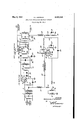
- the drawing shows a schematicdiagram of the invention disclosed.
- each of I. F. selector circuits l, 2, 3 and 4 will be tuned to the operating I. F. value of 'l2 mc., with sufficient dampingA being introduced by respective shunt damping resistors l', 2.', 3' and 4 to impart a passband width of about 12 mc. to each selector circuit.
- Each reso* nant selector circuit prior to circuit l will, also, have a suitable pass band width of the ordery of l2 mc.
- the selector circuit l may be coupled to the output electrodes of a suitable converter tube (not shown), or to the output electrodes of a preceding I. F. amplifier tube.
- the coils of selector circuits I to 4 inclusive are schematically indicated by arrows as being of the adjustable in ductance type, more particularly of the adjustable iron core type.
- Selector circuit 3 couples the output electrodes of tube 5 to the input electrodes of tube 6.
- the use of a single selector circuit 3 between tubes 5 and 6 tends tc provide less phase shift than would be the case with a double-tuned circuit.
- the use of the single selector circuit 3 tends to minimize phase shift and to insure against the circuits going into oscillation.
- the increased gain resulting from the use of doubletuned selector circuits may be considered as more than compensating for the increase of phase shift, and, therefore, the single selector circuit 3 may be replaced by a pair of coupled selector circuits, if desired.
- the FM detector circuit is not shown. but may be of any well-known type. For example. it may be constructed in the manner shown by S W. Seeley in his U. S. Patent No. 2.121.103. granted June 21, 1938, it may follow the teachings disclosed. by G. L. Usselman in his U. S. Patent No. 1,794,932; granted March 3, 1931, or itrmay be constructed along the lines of the detector circuit shown by J. D. Reid in his U. S. Patent No. 2.341.240, granted February 8, 1944.
- the Seeley detector circuit is preferred sincaas widely used, it utilizes a discriminator input circuit tuned to the I. F. value thereby facilitating alignment with the prior selector circuits. Whatever the nature of the FM detector circuit.
- AM components may appear on.
- the FM wave duringr the passage of the energy from the transmitter to the circuit 4.
- an amplifier tube whose characteristics were chosen to provide ready saturation of the tube for signals above a desired amplitude.
- Such a limiter device ref o russias a relatively high signal level at the input thereof.
- the usual limiters of the prior art do not function satisfactorily.
- MyV present invention overcomes these objections to the prior limiters, and provides a reliable and quick-acting means for substantially eliminating AM components on the FM wave prior to frequency discrimination.
- the AM component of the FM wave is subjected to detection, but without interfering with the normal I. F. amplification of the FM wave. This detection is secured in the circuit of tube S.
- the detected AM voltage is then applied, after amplification by tube 1, to prior amplier tube 5 in a sense to degenerate the gain thereof for the AM component.
- these functions are accomplished by virtue of the following circuit connections.
- Amplifier tube 5 has its control grid 8 connected to a source 9 of suitable negative bias through a path consisting of the coil of selector circuit 2, choke coil I0, resistor I I and slidable tap I2.
- the direct current source 9 is shunted by resistor I3 of the potentiometer I2, I3.
- the tap I2 also determines the xed operating bias for amplifier 1, since control grid I4 of tube 'I is connected to tap I2 through resistor I5.
- the cathodes of both tubes 5 and 'I are grounded.
- selector circuit 2 The low potential side of selector circuit 2 is returned to ground for I. F. currents by condenser I5.
- the plate II of amplifier tube 5 is connected to the -l-B voltage supply terminal through resistor 3', while the screen grid of the tube is operated at a suitable lower positive potential by virtue of voltage-reducing resistor I8.
- the screen grid is shunted to ground by condenser I9, which may be a 20 microfarad electrolytic condenser and which bypasses any detected AM voltage component (the degenerating voltage), and by condenser 20 which may be a paper condenser of 1500 micromicrofarads and which bypasses the I. F. currents.
- and I8 comprise a. voltage divider for deriving the correct tube voltages.
- the tube 6 has its control grid 22 coupled to the high alternating potential side of circuit 3 by condenser 23.
- the resistor 24 connects grid 22 to the grounded cathode of tube 6.
- Condensers 25 and 25 connected from the low potential side of selector circuit 3 may correspond respectively to condensers I9 and 20 and bypass to ground respectively the degenerative AM voltage and the I. F. voltage.
- the condenser 23 and grid leak resistor 24 cooperate to provide the usual leaky grid condenser network for an amplitude modulation detector operating on the principle of grid circuit rectification.
- the plate 21 of the tube B is connected to the +B voltage supply terminal through a lpath consisting of the coil of selector circuit 4, choke coil 28, resistor 29 and resistor 30.
- bypasses to ground the detected AM component, while condenser 32 returns the low potential side of circuit 4 to the grounded cathode of tube 6 for I. F. currents. Condenser 3l assists in getting the correct relation between phase shift and gain in the feedback loop.
- the screen grid 33 of tube 6 is bypassed to ground by condensers I9 and 20 which act respectively to bypass the ldegenerative AM component and the I. F. current, as in the case of the screen grid circuit of tube 5.
- the resistors 2l and I8 function to obtain correct screen. grid voltage, as in the case of resistors 2l and I8.
- the grid leak detector tube circuit concurrently detects any AM variations on the FM carrier wave and amplies the 'FM wave per se. Since the detector input circuit 3 is tuned to the operating I. F. value, and since no frequency discrim ⁇ tected AM voltage output of tube E.
- any AM components existing on the FMcarrier wave will be rectified by the Well known grid rectiiication action of thegridk leak detector tube.
- The. grid Vcircuit of tube ly effectivelyv functions like a diode circuit, the cathode and' grid 22. functioning as the diode, and provides rectified voltage of amplitude modulation frequency across resistor 2d.
- This rectified Voltage is applied to th'econtrol grid 22' of the tube which acts also as a screen grid amplifier tube for the detected AM voltage.
- 'Ihe amplified AM voltage output of tube is transmitted to the grid I4 of amplifier tube i. This is accomplished by connecting grid i4 through the coupling condenser d to the lower end or choke coil 28.
- the cathode 4l of tube 'l is grounded, while the control grid M is established at a desired negative bias by virtue of the adjustment of potentiometer tap i2.
- Th'e screen grid 42 of tube 'i is connected through resistor M to the +B terminal which supplies the plate 43, the resistor i5 functioning as the output load resistor of the amplifier tube 1.
- Screen grid 42 is, furthermore, returned to ground through a resistor 45 bypassed by condenser 41.
- Resistors 44 and 46 provide a voltage divider for obtaining correct screen voltage for tube 1.
- the voltage developed across resistor 45 is am plified voltage of amplitude modulation frequency, and it is applied to the control grid 8 of the I. F. amplifier tube 5.
- the voltage is applied to the control grid 8 in a degenerative sense.
- the path including condenser 50 and choke coil lli which has a relatively low impedance for the AM voltage but a relatively high impedance for I. F. currents, is a degenerative AM feedback path.
- The4 condenser 5l! is connected from the plate end of resistor e5 to the junction of resistor il and choke coil itl Hence, the AM voltage is employed inversely to modulate the FM wave energy applied to the control grid 8 by the selector circuits l and 2.
- each of tubes 5 and'l will include respective cathode bias resistorsof suitable value.
- the capacitance in each of the selector circuits may be provided by the inherent control grid to cathode capacity of each of the amplifier tubes. Suchinherent capacitance may be sufficient to provide the necessary tuning capacity for each selector circuit.
- a sourceV of angle modulated carrier waves an amplifier for the modulated Waves, a second amplifier for the amplied modulated Waves; means operatively associated with said second amplifier to render it operative as a detector' of'undesired amplitude variations in the ampliiiedi angle modulatedcarrier waves applied thereto, means for deriving from the output of said second amplier voltage representativev of detected undesired amplitude-variations, and a circuit for applying said derived voltage to said first ampliiier in a sense substantially to reduce' said undesired amplitude variations.
- a sourceV of anglemodulated carrier Waves coupled to the input electrodes of the first amplifier tube, at least one selector circuit tuned to a' desi-'redoperating frequency coupling the output i electrodes of thefir-st amplifier tube and theY input electrodes of'thevsecond amplifier tube, a leaky grid condenser network connected to the input' electrodesV of the second amplifier tube thereby ren-dering the latter operativeas a grid leak detectorfor undesired amplitude variations which may exist on said angle modulated carrier waves, a resonant selector circuit coupled to the output electrodes ofthe second amplifier tube across which is developed said angle modulated carrier Waves in amplified form, means in circuit with the output electrodes of the second amplifier tube for deriving therefrom detected amplitude variation voltage, and means for applying such detected voltage to the input, electrodes of said first amplifier tube in a degenerative sense thereby substantially to reduce said undesired amplitude variations.
- a source of phase or frequency modulated carrier Waves an amplifier foi' amplifying said waves, said amplifier producing undesired amplitude variations in the amplied waves, a grid leak detector tube circuit having input electrodes coupled to said amplifier, means in the output circuit of the grid leak detector tube for developing amplified phase or frequency modulated waves, and means responsive to detected amplitude variation voltage in the output circuit of said grid leak detector tube for controlling the gain of said amplifier in such a way as to balance or neutralize substantially all of said undesired amplitude variations.
- a first amplifier for the modulated waves a second amplifier for said modulated waves.
- a signalling system comprising a source f angle modulated carrier waves coupled to the input electrodes of a first amplier tube, a selector circuit tuned to a desired operating frequency coupling the output electrodes of the first amplifier tube to the input electrodes of a second amplifier tube, means connected to the input electrodes of the second amplifier tube for rendering the latter operative as a detector for undesired amplitude variations which may exist on -said angle modulated carrier Waves, means coupled to the output electrodes of the second amplifier tube to utilize angle modulated carrier Waves in amplified form, means in circuit with the output electrodes of the second amplifier tube for deriving therefrom detected amplitude variation voltage. and means for applying such detected volterfe to the input electrodes of 'said first amplifier tube in a degenerative sense thereby substantially to reduce said undesired amplitude variations.
- a source of phase or freo uency modulated carrier Waves an amplifier for amplifying said waves, said amplifier producing undesired amplitude variations in the amplified waves, a detector tube circuit having input electrodes coupled to said amplifier, mean-s in the output circuit of the detector tube for developing amplified phase or frequency modulated waves, and means responsive to detected amplitude variation vcltage in the output circuit of said detector tube for controlling the gain of said amplifier in such a way as to reduce substantially all of said undesired amplitude variations.
- a source of angle modulated carrier waves a source of angle modulated carrier waves.
- a source of angle modulated carrier waves a transmission network for the modulated Waves, an amplifier for the transmitted modulated Waves, means operatively associated with said amplifier to render it operative as a detector of undesired amplitude variations in the angle modulated carrier waves applied thereto, means for deriving from the output of said amplifier Voltage representative of detected undesired amplitude variations, and a circuit for utilizingsaid derived voltage to control the trans-4 mission of said network in a sense substantially to reduce said undesired amplitude variations.
- a pair of cascaded amplifier tubes a source of frequency modulated carrier Waves coupled to the input electrodes of the first amplifier tube, at least one selector ⁇ circuit timed to a desired operating frequency of the order of 72 megacycles coupling the output electrodes of the first amplifier tube and the input electrodes of the second amplifier tube, said selector circuit having a pass band Width of the order of 12 megacycles, a leaky grid condenser network connected to the input electrodes of the second amplier tube thereby rendering the latter operative as a grid leak detector for undesired amplitude variations which may exist on said frequency modulated carrier waves, a resonant selector circuit coupled to the output electrodes of the second amplifier tube across which is developed said frequency modulated carrier waves in amplified form, means in circuit with the output electrodes of the second amplifier tube for deriving therefrom detected amplitude variation voltage, and an amplifier for applying such detected voltage in amplified form to the input electrodes of said first amplier tube in a degenerative sense thereby substantially to
- a first amplifier for the modulated Waves a second amplier for said modulated waves
- means to render said second amplifier operative as a detector of undesired amplitude variations in the amplified angle modulated carrier waves applied thereto
Description
Mays, 1947.
N. l. KORMAN v AMPL'ITUDE MODULATION REDUCING CIRCUIT Filed July 29, 1944 Patented May 6, 1947 LITUDE MODULATIGN REDUCING CIRCUIT Nathaniel I. Korman, Camden, N. J., assigner to Radio Corporation of America, a corporation of vDelaware Application July 29, 1944, Serial No. 547,116
Claims. l
My present invention relates generally to a novel and improved system for substantially reducing undesired wave amplitude variations in a signalling system employing angle modulated carrier waves.
One of the important objects of my invention is to provide an improved means for eliminating, or at least substantially reducing, undesired amplitude variations or modulation oi angle modulated carrier waves by deriving from the latter any amplitude variation component which may exist on the waves, and then applying the derived component to a wave amplier in a sense to inversely .modulate= or degenerate, the amplier with respect to the amplitude variation compo nent of the modulated carrier waves whereby the undesired amplitude variations are effectively reduced.
Another important object of my present invention is to provide a circuit arrangement for a frequency modulation (FM) receiver, wherein amplitude modulation (AM) existing on the FM carrier wave is detected in a grid leak type ci detector whose output circuit concurrently feeds FM wave energy to a following FM demodulator network, the detected AM voltage being amplied and applied to an ampliiier stage preceding the demodulator in such a phase as degeneratively to decrease the amplitude modulation on the FM carrier wave.
Another object of my invention is to provide an improved system for removing amplitude variations from FM carrier waves which is efficient and effective for ultra-high frequencies as high as 100 megacycles (mc.) or higher, and which is not dependent upon a relatively high level of input signal energy as is the case with the various known forms of limiters of the readily-saturable ampliiier type.
While my present invention is described herein as embodied in the intermediate frequency (I. F.) ampliiier section of a receiver of the superheterodyne type, it is t0 be understood that such an embodiment is purely illustrative. My invention is readily applicable to any signalling system employing angle modulated carrier waves, be the system a receiver or a transmitter. The generic term angle modulated carrier wave includes an FM carrier wave or a phase modulated (PM) carrier wave, or carrier waves modulated by hybrid, or mixed, FM and PM characteristics. As those skilled in the art of radio communication well know, an FM wave is one whose carrier frequency is varied or deviated from the normal or center frequency value in accordance with the de-emphasis or correction networks at the modulation signal amplifier of the receiver.
Assuming for the purposes of this application that the system described is an FM receiverv of the superheterodyne type, only so much of they receiver as includes the I. F. amplier is shown in the drawing since my invention is applicable to that portion of the system.A However, the invention is equally applicable to any other part of the system prior to the I. F. networks, in that the carrier frequency range and theV frequency variation range` of each received modulated carrier Wave are not critical so far as the operationY of my invention is concerned. For example, my improved limiting circuit will function in a satis-v factory manner in the presently-assigned 42 to 50 megacycles (me.) FM broadcast band where each transmitter is permitted an overall frequency swing of 150 kilocycles (kc). The present limiting circuit has advantages for the -very high radio frequencies, those for example inthe range of 3000 to 30,000 mc. The I. F. value of the receiver could suitably be chosen from a range of 2 to the order of mc., and the overall frequency swing can be over relatively narrow ranges below kc. or over wide ranges as high as 12 mc. or above. The modulating signals may be in the audio frequency range, or in the video frequency range. l'n the latter case the overall frequency swing of the transmitter carrier will be relatively high.
The drawing shows a schematicdiagram of the invention disclosed.
Before describing the details of construction of my invention, it is pointed out` that it is assumed that the operating I. F. valueV is 72 mc., and that the selector circuits are constructed to accommodate and pass an overall frequency swing of 12 mc.y In such case each of I. F. selector circuits l, 2, 3 and 4 will be tuned to the operating I. F. value of 'l2 mc., with sufficient dampingA being introduced by respective shunt damping resistors l', 2.', 3' and 4 to impart a passband width of about 12 mc. to each selector circuit. Each reso* nant selector circuit prior to circuit l will, also, have a suitable pass band width of the ordery of l2 mc. The selector circuit l may be coupled to the output electrodes of a suitable converter tube (not shown), or to the output electrodes of a preceding I. F. amplifier tube. The coils of selector circuits I to 4 inclusive are schematically indicated by arrows as being of the adjustable in ductance type, more particularly of the adjustable iron core type.
The I. F. amplifier tubes 5 and I5, which for example may be 6AK5 type tubes, are cascaded. Selector circuit 3 couples the output electrodes of tube 5 to the input electrodes of tube 6.
The use of a single selector circuit 3 between tubes 5 and 6 tends tc provide less phase shift than would be the case with a double-tuned circuit. Hence, in the present degenerative circuit the use of the single selector circuit 3 tends to minimize phase shift and to insure against the circuits going into oscillation. However, the increased gain resulting from the use of doubletuned selector circuits may be considered as more than compensating for the increase of phase shift, and, therefore, the single selector circuit 3 may be replaced by a pair of coupled selector circuits, if desired. After the desired amplification by tubes 5 and 5 the I. F. signal energy is transmitted to any suitable FM detector circuit. In other words the amplified I. F. signal voltage developed across the tuned selector circuit 4, arranged in the plate circuit of tube 5, is demodulated to provide the modulation signals which originally were applied to the carrier at the transmitter.
The FM detector circuit is not shown. but may be of any well-known type. For example. it may be constructed in the manner shown by S W. Seeley in his U. S. Patent No. 2.121.103. granted June 21, 1938, it may follow the teachings disclosed. by G. L. Usselman in his U. S. Patent No. 1,794,932; granted March 3, 1931, or itrmay be constructed along the lines of the detector circuit shown by J. D. Reid in his U. S. Patent No. 2.341.240, granted February 8, 1944. The Seeley detector circuit is preferred sincaas widely used, it utilizes a discriminator input circuit tuned to the I. F. value thereby facilitating alignment with the prior selector circuits. Whatever the nature of the FM detector circuit. there should be developed across selector circuit 4 signal energy which varies in frequency and not in amplitude. Any AM component or effect which may exist on the FM carrier wave will be evidenced in the FM discriminator-detector output as a distortion product since it is not desired that any amplitude variation exist at the transmitter.
However. there are many reasons why AM components may appear on. the FM wave duringr the passage of the energy from the transmitter to the circuit 4. Noise impulses, selective fading. curvature of Yreceiver selector response curves, tube noise, power supply ripples: these are but a few sources of amplitude modulation of the FM carrier. In the past there has been employed as an amplitude limiting device an amplifier tube whose characteristics were chosen to provide ready saturation of the tube for signals above a desired amplitude. Such a limiter device ref o uires a relatively high signal level at the input thereof. Further, at the very high radio frequencies the usual limiters of the prior art do not function satisfactorily.
MyV present invention overcomes these objections to the prior limiters, and provides a reliable and quick-acting means for substantially eliminating AM components on the FM wave prior to frequency discrimination. According to my method the AM component of the FM wave is subjected to detection, but without interfering with the normal I. F. amplification of the FM wave. This detection is secured in the circuit of tube S. The detected AM voltage is then applied, after amplification by tube 1, to prior amplier tube 5 in a sense to degenerate the gain thereof for the AM component. Specifically, these functions are accomplished by virtue of the following circuit connections. Amplifier tube 5 has its control grid 8 connected to a source 9 of suitable negative bias through a path consisting of the coil of selector circuit 2, choke coil I0, resistor I I and slidable tap I2. The direct current source 9 is shunted by resistor I3 of the potentiometer I2, I3. The tap I2 also determines the xed operating bias for amplifier 1, since control grid I4 of tube 'I is connected to tap I2 through resistor I5. The cathodes of both tubes 5 and 'I are grounded.
The low potential side of selector circuit 2 is returned to ground for I. F. currents by condenser I5. The plate II of amplifier tube 5 is connected to the -l-B voltage supply terminal through resistor 3', while the screen grid of the tube is operated at a suitable lower positive potential by virtue of voltage-reducing resistor I8. The screen grid is shunted to ground by condenser I9, which may be a 20 microfarad electrolytic condenser and which bypasses any detected AM voltage component (the degenerating voltage), and by condenser 20 which may be a paper condenser of 1500 micromicrofarads and which bypasses the I. F. currents. 'I'he reason for using both condensers I9 and 20 is that the relatively large electrolytic condenser I9 may nevertheless have substantial impedance to the I. F. currents. Resistors 2| and I8 comprise a. voltage divider for deriving the correct tube voltages.
The tube 6 has its control grid 22 coupled to the high alternating potential side of circuit 3 by condenser 23. The resistor 24 connects grid 22 to the grounded cathode of tube 6. Condensers 25 and 25 connected from the low potential side of selector circuit 3 may correspond respectively to condensers I9 and 20 and bypass to ground respectively the degenerative AM voltage and the I. F. voltage. The condenser 23 and grid leak resistor 24 cooperate to provide the usual leaky grid condenser network for an amplitude modulation detector operating on the principle of grid circuit rectification. The plate 21 of the tube B is connected to the +B voltage supply terminal through a lpath consisting of the coil of selector circuit 4, choke coil 28, resistor 29 and resistor 30. Condenser 3| bypasses to ground the detected AM component, while condenser 32 returns the low potential side of circuit 4 to the grounded cathode of tube 6 for I. F. currents. Condenser 3l assists in getting the correct relation between phase shift and gain in the feedback loop.
The screen grid 33 of tube 6 is bypassed to ground by condensers I9 and 20 which act respectively to bypass the ldegenerative AM component and the I. F. current, as in the case of the screen grid circuit of tube 5. The resistors 2l and I8 function to obtain correct screen. grid voltage, as in the case of resistors 2l and I8. The grid leak detector tube circuit concurrently detects any AM variations on the FM carrier wave and amplies the 'FM wave per se. Since the detector input circuit 3 is tuned to the operating I. F. value, and since no frequency discrim` tected AM voltage output of tube E.
5. inationtakes place at circuit 3 so asto'translate the FM Wave into a corresponding AM wave, the grid rleak detector action will not aflect the rcproduction by the FM detector circuit of the frequency Variations of the FM carrier Wave. In otherwords the tube 6 will actin .the'manner of an I. F. amplifier for the FM carrier Wave energy.
However, any AM components existing on the FMcarrier wave will be rectified by the Well known grid rectiiication action of thegridk leak detector tube. The. grid Vcircuit of tube ly effectivelyv functions like a diode circuit, the cathode and' grid 22. functioning as the diode, and provides rectified voltage of amplitude modulation frequency across resistor 2d. This rectified Voltage is applied to th'econtrol grid 22' of the tube which acts also as a screen grid amplifier tube for the detected AM voltage. 'Ihe amplified AM voltage output of tube is transmitted to the grid I4 of amplifier tube i. This is accomplished by connecting grid i4 through the coupling condenser d to the lower end or choke coil 28. The cathode 4l of tube 'l is grounded, while the control grid M is established at a desired negative bias by virtue of the adjustment of potentiometer tap i2. Th'e screen grid 42 of tube 'i is connected through resistor M to the +B terminal which supplies the plate 43, the resistor i5 functioning as the output load resistor of the amplifier tube 1. Screen grid 42 is, furthermore, returned to ground through a resistor 45 bypassed by condenser 41. Resistors 44 and 46 provide a voltage divider for obtaining correct screen voltage for tube 1.
The voltage developed across resistor 45 is am plified voltage of amplitude modulation frequency, and it is applied to the control grid 8 of the I. F. amplifier tube 5. The voltage is applied to the control grid 8 in a degenerative sense. In other words the path including condenser 50 and choke coil lli, which has a relatively low impedance for the AM voltage but a relatively high impedance for I. F. currents, is a degenerative AM feedback path. The4 condenser 5l! is connected from the plate end of resistor e5 to the junction of resistor il and choke coil itl Hence, the AM voltage is employed inversely to modulate the FM wave energy applied to the control grid 8 by the selector circuits l and 2. This inverse modulation of the FM wavel energy is actually a degenerative control of the gain of amplifier tube 5. In other Words the gain control of tubeE is in accordance with the AM envelope of the de- It may, also, be said that the tube 6, including the amplifier 1, and its connection back to the control grid circuit of tube 5 functions as a fast-acting gain control circuit which acts to reduce the gain of tube 5 in proportion to thetendency of the AM eects on the FM carrier Wave to increase.
Let it be assumed; in explaining the operation of the circuit more fully, th'at for one reason or another the FM carrier Wave energy at the receiving system becomes amplitude modulated. There will' then be developed across the resistor 24 rectified Voltage of amplitude modulation frequency Whose Wave form follows that of the amplitude modulation of the FM carrier Wave. This means that the grid end of resistor 24 will becomel increasingly negative as the amplitude of the FM carrier Wave increases, and thus Will reduce the plate current ow through resistors 2% and 3i?. As a result the plate end of resistor 29 will become increasingly positive in potential with the result that the control grid voltage of tube 1 willincrease. This causesthe space current owthrough resistor to increase thereby rendering the plate end of resistor 45 Vless positive. The plate end of resistor 45 being connected back to thegrid of tubev 5, this grid Will becomer morer negative and thus act to decreasel the gain of tube 5for the FM Wave. Th'us, the action of the circuit is tov oppose any change in the amplitude of the FM Wave.
Since the modulation component of voltage drop across resistor 24 depends upon the existence of amplitude modulation on the FM carrier wave, it necessarily` follows that when the amplitude modulation on the carrier Wave disappears the voltageY across resistor 2d will also'disappear. As a result the tube 6 will operate with its normal space current ow, andv tube 1 will not have any alternating voltage applied to its grid. It should be noted that th'e gain of tube 1 is not changed by the presence of amplitude modulation. In the same Way the disappearance of the AM component of the FM carrier Wave will result in tube 5 functioning as a normal I. F. ampliiier. It will, therefore,` be seen that the controlfaction is automatic; and responds at once to the appearance of any AM. component on the FM carrier wave. In this WayV there is' delivered to the FM detector circuit modulated carrier wave energy which is frequency-variable and is substantially free of any amplitude modulation.
It may be desirable in Asome instances to eliminate the source of negative bias 9 and the common potentiometer IZ, YI3 for the control grids 8 and I4. In such case the cathode circuit of each of tubes 5 and'l will include respective cathode bias resistorsof suitable value. Furthermore, in the case Where the operating frequency in the system is sufficiently high, the capacitance in each of the selector circuits may be provided by the inherent control grid to cathode capacity of each of the amplifier tubes. Suchinherent capacitance may be sufficient to provide the necessary tuning capacity for each selector circuit.
While I have indicated and described a system for carrying my invention into effect, it Will'be apparent to one skilled in the art that my invention is by no means limited to thel particular organization shown and described, but th'at many modiiications may be made without departing from the scope of my invention.
What I claim is:
l. In combination. a sourceV of angle modulated carrier waves, an amplifier for the modulated Waves, a second amplifier for the amplied modulated Waves; means operatively associated with said second amplifier to render it operative as a detector' of'undesired amplitude variations in the ampliiiedi angle modulatedcarrier waves applied thereto, means for deriving from the output of said second amplier voltage representativev of detected undesired amplitude-variations, and a circuit for applying said derived voltage to said first ampliiier in a sense substantially to reduce' said undesired amplitude variations.
2. In combination, apairl of cascadedamplifier tubes, a sourceV of anglemodulated carrier Waves coupled to the input electrodes of the first amplifier tube, at least one selector circuit tuned to a' desi-'redoperating frequency coupling the output i electrodes of thefir-st amplifier tube and theY input electrodes of'thevsecond amplifier tube, a leaky grid condenser network connected to the input' electrodesV of the second amplifier tube thereby ren-dering the latter operativeas a grid leak detectorfor undesired amplitude variations which may exist on said angle modulated carrier waves, a resonant selector circuit coupled to the output electrodes ofthe second amplifier tube across which is developed said angle modulated carrier Waves in amplified form, means in circuit with the output electrodes of the second amplifier tube for deriving therefrom detected amplitude variation voltage, and means for applying such detected voltage to the input, electrodes of said first amplifier tube in a degenerative sense thereby substantially to reduce said undesired amplitude variations.
3. In combination, a source of phase or frequency modulated carrier Waves, an amplifier foi' amplifying said waves, said amplifier producing undesired amplitude variations in the amplied waves, a grid leak detector tube circuit having input electrodes coupled to said amplifier, means in the output circuit of the grid leak detector tube for developing amplified phase or frequency modulated waves, and means responsive to detected amplitude variation voltage in the output circuit of said grid leak detector tube for controlling the gain of said amplifier in such a way as to balance or neutralize substantially all of said undesired amplitude variations.
4. In combination with a source of frequency modulated carrier waves, a first amplifier for the modulated waves, a second amplifier for said modulated waves. means to render said second amplifier operative as a detector of undesired amplitude variations in the amplified angle modulated carrier waves applied thereto, means for deriving from the output of said second amplifier detected undesired amplitude variation voltage, and means for applying said derived voltage to said first amplifier in a degenerative sense thereby to reduce said undesired amplitude variations.
5. A signalling system comprising a source f angle modulated carrier waves coupled to the input electrodes of a first amplier tube, a selector circuit tuned to a desired operating frequency coupling the output electrodes of the first amplifier tube to the input electrodes of a second amplifier tube, means connected to the input electrodes of the second amplifier tube for rendering the latter operative as a detector for undesired amplitude variations which may exist on -said angle modulated carrier Waves, means coupled to the output electrodes of the second amplifier tube to utilize angle modulated carrier Waves in amplified form, means in circuit with the output electrodes of the second amplifier tube for deriving therefrom detected amplitude variation voltage. and means for applying such detected volterfe to the input electrodes of 'said first amplifier tube in a degenerative sense thereby substantially to reduce said undesired amplitude variations.
6. In combination, a source of phase or freo uency modulated carrier Waves, an amplifier for amplifying said waves, said amplifier producing undesired amplitude variations in the amplified waves, a detector tube circuit having input electrodes coupled to said amplifier, mean-s in the output circuit of the detector tube for developing amplified phase or frequency modulated waves, and means responsive to detected amplitude variation vcltage in the output circuit of said detector tube for controlling the gain of said amplifier in such a way as to reduce substantially all of said undesired amplitude variations.
'7. In combination. a source of angle modulated carrier waves. a first tube for transmitting said waves, said tube producing undesired amplitude variations in the amplified waves, a detectorl tube circuit having input electrodes coupled to said first tube, means in the output circuit of the detector tube for developing angle modulated waves, and means responsive to' detected amplitude variation voltage in the output circuit of said detector tube for degeneratively controlling the gain of said first tube in such a way as to neutralize substantially all of said undesired amplitude variations.
8. In combination, a source of angle modulated carrier waves, a transmission network for the modulated Waves, an amplifier for the transmitted modulated Waves, means operatively associated with said amplifier to render it operative as a detector of undesired amplitude variations in the angle modulated carrier waves applied thereto, means for deriving from the output of said amplifier Voltage representative of detected undesired amplitude variations, and a circuit for utilizingsaid derived voltage to control the trans-4 mission of said network in a sense substantially to reduce said undesired amplitude variations.
9. In combination, a pair of cascaded amplifier tubes, a source of frequency modulated carrier Waves coupled to the input electrodes of the first amplifier tube, at least one selector` circuit timed to a desired operating frequency of the order of 72 megacycles coupling the output electrodes of the first amplifier tube and the input electrodes of the second amplifier tube, said selector circuit having a pass band Width of the order of 12 megacycles, a leaky grid condenser network connected to the input electrodes of the second amplier tube thereby rendering the latter operative as a grid leak detector for undesired amplitude variations which may exist on said frequency modulated carrier waves, a resonant selector circuit coupled to the output electrodes of the second amplifier tube across which is developed said frequency modulated carrier waves in amplified form, means in circuit with the output electrodes of the second amplifier tube for deriving therefrom detected amplitude variation voltage, and an amplifier for applying such detected voltage in amplified form to the input electrodes of said first amplier tube in a degenerative sense thereby substantially to reduce said undesired amplitude variations.
10. In combination with a source of frequency modulated carrier waves, a first amplifier for the modulated Waves, a second amplier for said modulated waves, means to render said second amplifier operative as a detector of undesired amplitude variations in the amplified angle modulated carrier waves applied thereto, means for deriving from the output of said Second amplifier detected undesired amplitude variation voltage, an amplifier for said detectedY voltage, and a capacity feedback path for applying said amplified detected voltage to said first amplifier in a degenerative sense thereby to reduce said undesired amplitude variations.
N ATHANIEL I. KORMAN.
REFERENCES CITED The following references are of record in the filelof this patent:
UNITED STATES PATENTS Number Name Date 2,250,862 Farrington July 29, 1941 2,282,092 Roberts May 5, 1942
Priority Applications (1)
| Application Number | Priority Date | Filing Date | Title |
|---|---|---|---|
| US547116A US2420249A (en) | 1944-07-29 | 1944-07-29 | Amplitude modulation reducing circuit |
Applications Claiming Priority (1)
| Application Number | Priority Date | Filing Date | Title |
|---|---|---|---|
| US547116A US2420249A (en) | 1944-07-29 | 1944-07-29 | Amplitude modulation reducing circuit |
Publications (1)
| Publication Number | Publication Date |
|---|---|
| US2420249A true US2420249A (en) | 1947-05-06 |
Family
ID=24183400
Family Applications (1)
| Application Number | Title | Priority Date | Filing Date |
|---|---|---|---|
| US547116A Expired - Lifetime US2420249A (en) | 1944-07-29 | 1944-07-29 | Amplitude modulation reducing circuit |
Country Status (1)
| Country | Link |
|---|---|
| US (1) | US2420249A (en) |
Cited By (7)
| Publication number | Priority date | Publication date | Assignee | Title |
|---|---|---|---|---|
| US2510640A (en) * | 1946-05-31 | 1950-06-06 | Rca Corp | Stabilized high-frequency amplifier |
| US2654026A (en) * | 1948-10-27 | 1953-09-29 | Hartford Nat Bank & Trust Co | Radio circuit arrangement |
| US2686259A (en) * | 1950-08-30 | 1954-08-10 | Rca Corp | Reduction of amplitude modulation in frequency modulation receivers |
| US2698899A (en) * | 1948-12-02 | 1955-01-04 | Hartford Nat Bank & Trust Co | Circuit arrangement for receiving and demodulating frequency-modulated oscillations |
| US2790943A (en) * | 1951-08-27 | 1957-04-30 | Honeywell Regulator Co | Multiple gain amplifier for servo control |
| US3027519A (en) * | 1959-04-21 | 1962-03-27 | Bendix Corp | Gain-versus-bandwidth control amplifier particularly adapted for television circuitry |
| US3155917A (en) * | 1959-05-07 | 1964-11-03 | Honeywell Inc | Electronic apparatus |
Citations (2)
| Publication number | Priority date | Publication date | Assignee | Title |
|---|---|---|---|---|
| US2250862A (en) * | 1940-07-16 | 1941-07-29 | Hazeltine Corp | Combination amplitude-modulationfrequency-modulation receiver |
| US2282092A (en) * | 1941-03-26 | 1942-05-05 | Rca Corp | Frequency modulation receiver |
-
1944
- 1944-07-29 US US547116A patent/US2420249A/en not_active Expired - Lifetime
Patent Citations (2)
| Publication number | Priority date | Publication date | Assignee | Title |
|---|---|---|---|---|
| US2250862A (en) * | 1940-07-16 | 1941-07-29 | Hazeltine Corp | Combination amplitude-modulationfrequency-modulation receiver |
| US2282092A (en) * | 1941-03-26 | 1942-05-05 | Rca Corp | Frequency modulation receiver |
Cited By (7)
| Publication number | Priority date | Publication date | Assignee | Title |
|---|---|---|---|---|
| US2510640A (en) * | 1946-05-31 | 1950-06-06 | Rca Corp | Stabilized high-frequency amplifier |
| US2654026A (en) * | 1948-10-27 | 1953-09-29 | Hartford Nat Bank & Trust Co | Radio circuit arrangement |
| US2698899A (en) * | 1948-12-02 | 1955-01-04 | Hartford Nat Bank & Trust Co | Circuit arrangement for receiving and demodulating frequency-modulated oscillations |
| US2686259A (en) * | 1950-08-30 | 1954-08-10 | Rca Corp | Reduction of amplitude modulation in frequency modulation receivers |
| US2790943A (en) * | 1951-08-27 | 1957-04-30 | Honeywell Regulator Co | Multiple gain amplifier for servo control |
| US3027519A (en) * | 1959-04-21 | 1962-03-27 | Bendix Corp | Gain-versus-bandwidth control amplifier particularly adapted for television circuitry |
| US3155917A (en) * | 1959-05-07 | 1964-11-03 | Honeywell Inc | Electronic apparatus |
Similar Documents
| Publication | Publication Date | Title |
|---|---|---|
| US2152515A (en) | Automatic signal interference control | |
| US2410983A (en) | Discriminator-rectifier circuit | |
| US2412482A (en) | Discriminator-rectifier circuits | |
| US2286442A (en) | Amplitude limiter circuit | |
| US2420249A (en) | Amplitude modulation reducing circuit | |
| US2361625A (en) | Frequency and phase modulation receiver | |
| US2273097A (en) | Frequency modulated wave receiver | |
| US2519890A (en) | Angle modulated wave receiver | |
| US3172040A (en) | Am/fm receiver having automatic gain control | |
| US2410981A (en) | Superregenerative receiver circuits | |
| US2262841A (en) | Automatic gain expansion circuit | |
| US2245685A (en) | Automatic frequency control system | |
| US2273110A (en) | Frequency modulated wave receiver | |
| US2496818A (en) | Angle modulation detector | |
| US2473790A (en) | Automatic frequency control circuits | |
| US2177713A (en) | Frequency-selective network | |
| US2528182A (en) | Frequency discriminator network | |
| US2488410A (en) | Control circuits for alternating current transmission networks | |
| US2128996A (en) | Automatic volume control circuits | |
| US2144935A (en) | Automatic volume control circuits | |
| US2286410A (en) | Frequency modulation receiver tuning indicator | |
| US2488606A (en) | Frequency modulation receiver | |
| US2344699A (en) | Amplitude modulation limiter circuit | |
| US2489948A (en) | Radio receiving system | |
| US2595441A (en) | Angle modulated carrier wave receiver |