US20150177458A1 - Bonding of heterogeneous material grown on silicon to a silicon photonic circuit - Google Patents
Bonding of heterogeneous material grown on silicon to a silicon photonic circuit Download PDFInfo
- Publication number
- US20150177458A1 US20150177458A1 US14/577,938 US201414577938A US2015177458A1 US 20150177458 A1 US20150177458 A1 US 20150177458A1 US 201414577938 A US201414577938 A US 201414577938A US 2015177458 A1 US2015177458 A1 US 2015177458A1
- Authority
- US
- United States
- Prior art keywords
- wafer
- iii
- layer
- silicon
- epitaxial layer
- Prior art date
- Legal status (The legal status is an assumption and is not a legal conclusion. Google has not performed a legal analysis and makes no representation as to the accuracy of the status listed.)
- Granted
Links
- XUIMIQQOPSSXEZ-UHFFFAOYSA-N Silicon Chemical compound [Si] XUIMIQQOPSSXEZ-UHFFFAOYSA-N 0.000 title claims abstract description 107
- 229910052710 silicon Inorganic materials 0.000 title claims abstract description 107
- 239000010703 silicon Substances 0.000 title claims abstract description 107
- 239000000463 material Substances 0.000 title description 26
- 239000004065 semiconductor Substances 0.000 claims abstract description 91
- 239000000758 substrate Substances 0.000 claims abstract description 71
- 238000004519 manufacturing process Methods 0.000 claims abstract description 30
- 238000000151 deposition Methods 0.000 claims abstract description 4
- 235000012431 wafers Nutrition 0.000 claims description 140
- 238000000034 method Methods 0.000 claims description 34
- VYPSYNLAJGMNEJ-UHFFFAOYSA-N Silicium dioxide Chemical compound O=[Si]=O VYPSYNLAJGMNEJ-UHFFFAOYSA-N 0.000 claims description 25
- 229910052751 metal Inorganic materials 0.000 claims description 20
- 239000002184 metal Substances 0.000 claims description 20
- 230000005693 optoelectronics Effects 0.000 claims description 20
- 230000003287 optical effect Effects 0.000 claims description 17
- 230000008569 process Effects 0.000 claims description 16
- 239000000377 silicon dioxide Substances 0.000 claims description 12
- 235000012239 silicon dioxide Nutrition 0.000 claims description 8
- 238000000137 annealing Methods 0.000 claims description 7
- 239000012212 insulator Substances 0.000 claims description 7
- 238000012545 processing Methods 0.000 claims description 7
- 229910000577 Silicon-germanium Inorganic materials 0.000 claims description 6
- 239000002096 quantum dot Substances 0.000 claims description 6
- LEVVHYCKPQWKOP-UHFFFAOYSA-N [Si].[Ge] Chemical compound [Si].[Ge] LEVVHYCKPQWKOP-UHFFFAOYSA-N 0.000 claims description 3
- 239000006096 absorbing agent Substances 0.000 claims description 3
- 229910052732 germanium Inorganic materials 0.000 claims description 3
- GNPVGFCGXDBREM-UHFFFAOYSA-N germanium atom Chemical compound [Ge] GNPVGFCGXDBREM-UHFFFAOYSA-N 0.000 claims description 3
- 230000010287 polarization Effects 0.000 claims description 3
- VEALVRVVWBQVSL-UHFFFAOYSA-N strontium titanate Chemical compound [Sr+2].[O-][Ti]([O-])=O VEALVRVVWBQVSL-UHFFFAOYSA-N 0.000 claims description 3
- 230000002209 hydrophobic effect Effects 0.000 claims description 2
- 229920000642 polymer Polymers 0.000 claims description 2
- 229910000679 solder Inorganic materials 0.000 claims description 2
- 230000008878 coupling Effects 0.000 description 12
- 238000010168 coupling process Methods 0.000 description 12
- 238000005859 coupling reaction Methods 0.000 description 12
- 238000004891 communication Methods 0.000 description 9
- 230000008901 benefit Effects 0.000 description 7
- 238000013459 approach Methods 0.000 description 4
- 230000007547 defect Effects 0.000 description 4
- RYGMFSIKBFXOCR-UHFFFAOYSA-N Copper Chemical compound [Cu] RYGMFSIKBFXOCR-UHFFFAOYSA-N 0.000 description 3
- KRHYYFGTRYWZRS-UHFFFAOYSA-N Fluorane Chemical compound F KRHYYFGTRYWZRS-UHFFFAOYSA-N 0.000 description 3
- FTWRSWRBSVXQPI-UHFFFAOYSA-N alumanylidynearsane;gallanylidynearsane Chemical compound [As]#[Al].[As]#[Ga] FTWRSWRBSVXQPI-UHFFFAOYSA-N 0.000 description 3
- 229910052802 copper Inorganic materials 0.000 description 3
- 239000010949 copper Substances 0.000 description 3
- 238000000407 epitaxy Methods 0.000 description 3
- 230000010354 integration Effects 0.000 description 3
- IJGRMHOSHXDMSA-UHFFFAOYSA-N Atomic nitrogen Chemical compound N#N IJGRMHOSHXDMSA-UHFFFAOYSA-N 0.000 description 2
- 229910052581 Si3N4 Inorganic materials 0.000 description 2
- UMIVXZPTRXBADB-UHFFFAOYSA-N benzocyclobutene Chemical compound C1=CC=C2CCC2=C1 UMIVXZPTRXBADB-UHFFFAOYSA-N 0.000 description 2
- 238000005516 engineering process Methods 0.000 description 2
- 238000002248 hydride vapour-phase epitaxy Methods 0.000 description 2
- HQVNEWCFYHHQES-UHFFFAOYSA-N silicon nitride Chemical compound N12[Si]34N5[Si]62N3[Si]51N64 HQVNEWCFYHHQES-UHFFFAOYSA-N 0.000 description 2
- 125000006850 spacer group Chemical group 0.000 description 2
- JBRZTFJDHDCESZ-UHFFFAOYSA-N AsGa Chemical compound [As]#[Ga] JBRZTFJDHDCESZ-UHFFFAOYSA-N 0.000 description 1
- GYHNNYVSQQEPJS-UHFFFAOYSA-N Gallium Chemical compound [Ga] GYHNNYVSQQEPJS-UHFFFAOYSA-N 0.000 description 1
- JMASRVWKEDWRBT-UHFFFAOYSA-N Gallium nitride Chemical compound [Ga]#N JMASRVWKEDWRBT-UHFFFAOYSA-N 0.000 description 1
- GPXJNWSHGFTCBW-UHFFFAOYSA-N Indium phosphide Chemical compound [In]#P GPXJNWSHGFTCBW-UHFFFAOYSA-N 0.000 description 1
- OAICVXFJPJFONN-UHFFFAOYSA-N Phosphorus Chemical compound [P] OAICVXFJPJFONN-UHFFFAOYSA-N 0.000 description 1
- 229910052782 aluminium Inorganic materials 0.000 description 1
- XAGFODPZIPBFFR-UHFFFAOYSA-N aluminium Chemical compound [Al] XAGFODPZIPBFFR-UHFFFAOYSA-N 0.000 description 1
- MDPILPRLPQYEEN-UHFFFAOYSA-N aluminium arsenide Chemical compound [As]#[Al] MDPILPRLPQYEEN-UHFFFAOYSA-N 0.000 description 1
- 229910052787 antimony Inorganic materials 0.000 description 1
- WATWJIUSRGPENY-UHFFFAOYSA-N antimony atom Chemical compound [Sb] WATWJIUSRGPENY-UHFFFAOYSA-N 0.000 description 1
- 229910052785 arsenic Inorganic materials 0.000 description 1
- RQNWIZPPADIBDY-UHFFFAOYSA-N arsenic atom Chemical compound [As] RQNWIZPPADIBDY-UHFFFAOYSA-N 0.000 description 1
- 238000005229 chemical vapour deposition Methods 0.000 description 1
- 238000007796 conventional method Methods 0.000 description 1
- 238000001816 cooling Methods 0.000 description 1
- 239000013078 crystal Substances 0.000 description 1
- 238000013500 data storage Methods 0.000 description 1
- 230000007123 defense Effects 0.000 description 1
- 230000001419 dependent effect Effects 0.000 description 1
- 239000003989 dielectric material Substances 0.000 description 1
- 229910052733 gallium Inorganic materials 0.000 description 1
- HZXMRANICFIONG-UHFFFAOYSA-N gallium phosphide Chemical compound [Ga]#P HZXMRANICFIONG-UHFFFAOYSA-N 0.000 description 1
- 229910021478 group 5 element Inorganic materials 0.000 description 1
- 238000010438 heat treatment Methods 0.000 description 1
- 229910052738 indium Inorganic materials 0.000 description 1
- RPQDHPTXJYYUPQ-UHFFFAOYSA-N indium arsenide Chemical compound [In]#[As] RPQDHPTXJYYUPQ-UHFFFAOYSA-N 0.000 description 1
- APFVFJFRJDLVQX-UHFFFAOYSA-N indium atom Chemical compound [In] APFVFJFRJDLVQX-UHFFFAOYSA-N 0.000 description 1
- 238000012986 modification Methods 0.000 description 1
- 230000004048 modification Effects 0.000 description 1
- 238000001451 molecular beam epitaxy Methods 0.000 description 1
- 229910021421 monocrystalline silicon Inorganic materials 0.000 description 1
- QPJSUIGXIBEQAC-UHFFFAOYSA-N n-(2,4-dichloro-5-propan-2-yloxyphenyl)acetamide Chemical compound CC(C)OC1=CC(NC(C)=O)=C(Cl)C=C1Cl QPJSUIGXIBEQAC-UHFFFAOYSA-N 0.000 description 1
- 229910052757 nitrogen Inorganic materials 0.000 description 1
- 239000012071 phase Substances 0.000 description 1
- 229910052698 phosphorus Inorganic materials 0.000 description 1
- 239000011574 phosphorus Substances 0.000 description 1
- 230000009467 reduction Effects 0.000 description 1
- 238000011160 research Methods 0.000 description 1
- 229910052814 silicon oxide Inorganic materials 0.000 description 1
- 238000005476 soldering Methods 0.000 description 1
- 238000000927 vapour-phase epitaxy Methods 0.000 description 1
Images


Classifications
-
- G—PHYSICS
- G02—OPTICS
- G02B—OPTICAL ELEMENTS, SYSTEMS OR APPARATUS
- G02B6/00—Light guides; Structural details of arrangements comprising light guides and other optical elements, e.g. couplings
- G02B6/10—Light guides; Structural details of arrangements comprising light guides and other optical elements, e.g. couplings of the optical waveguide type
- G02B6/12—Light guides; Structural details of arrangements comprising light guides and other optical elements, e.g. couplings of the optical waveguide type of the integrated circuit kind
- G02B6/12007—Light guides; Structural details of arrangements comprising light guides and other optical elements, e.g. couplings of the optical waveguide type of the integrated circuit kind forming wavelength selective elements, e.g. multiplexer, demultiplexer
-
- G—PHYSICS
- G02—OPTICS
- G02B—OPTICAL ELEMENTS, SYSTEMS OR APPARATUS
- G02B6/00—Light guides; Structural details of arrangements comprising light guides and other optical elements, e.g. couplings
- G02B6/10—Light guides; Structural details of arrangements comprising light guides and other optical elements, e.g. couplings of the optical waveguide type
- G02B6/12—Light guides; Structural details of arrangements comprising light guides and other optical elements, e.g. couplings of the optical waveguide type of the integrated circuit kind
- G02B6/12002—Three-dimensional structures
-
- G—PHYSICS
- G02—OPTICS
- G02B—OPTICAL ELEMENTS, SYSTEMS OR APPARATUS
- G02B6/00—Light guides; Structural details of arrangements comprising light guides and other optical elements, e.g. couplings
- G02B6/10—Light guides; Structural details of arrangements comprising light guides and other optical elements, e.g. couplings of the optical waveguide type
- G02B6/12—Light guides; Structural details of arrangements comprising light guides and other optical elements, e.g. couplings of the optical waveguide type of the integrated circuit kind
- G02B6/13—Integrated optical circuits characterised by the manufacturing method
- G02B6/131—Integrated optical circuits characterised by the manufacturing method by using epitaxial growth
Definitions
- the present disclosure relates to integrated circuit fabrication, and in particular to fabrication of optoelectronic integrated circuits.
- Data communication or “Datacom” has traditionally relied on copper wires to transmit data from point to point.
- a copper communication bus may provide communication between a processor and a data storage medium in a household PC, or between servers in a data center. Communication via a traditional copper communication bus is well understood and benefits from the fact that both the endpoint and communication medium are electrical devices.
- Optical communication systems offer the promise of greater bandwidth and speed.
- optical communication systems suffer from the interface required between the optical communication system and electrical devices.
- coupling of optical components and electrical components typically results in electrical and optical coupling losses and/or signal distortions.
- PIC Photonic Integrated Circuit
- Si semiconductor material silicon
- III-V type semiconductors III-V type semiconductors
- These semiconductor materials include combinations of group III elements Aluminum (Al), Gallium (Ga), Indium (In) with group V elements Nitrogen (N), Phosphorus (P), Arsenic (As), and Antimony (Sb), and include combinations such as Gallium Arsenide (GaAs), Indium Phosphide (InP), Gallium Phosphide (GaP), Gallium Nitride (GaN), and Aluminum Gallium Arsenide (AlGaAs).
- a characteristic of III-V type semiconductors is the direct band gap, which allows for the fabrication of active optoelectronic devices such as lasers, photodetectors, and light-emitting diodes.
- III-V type semiconductor material is deposited directly on a silicon substrate or processed silicon layer.
- lattice constant differences between silicon and III-V type semiconductor materials results in fatal defects (e.g., dislocations) near the silicon/III-V interface.
- a buffer layer can be deposited between the silicon/III-V interface.
- thin layers can still represent a source of random, lossy defects that negatively impacts coupling between the active III-V devices and the passive silicon components (e.g., electrical circuits, waveguides, etc.).
- III-V type semiconductor material is grown on a native III-V type substrate having the same or similar lattice constant and then transferred to a silicon substrate.
- this approach is costly as the cost of producing III-V type semiconductor substrates is far greater than the cost of producing a silicon substrate.
- placement of the processed, active III-V device requires precise alignment between the device and the passive component (e.g., waveguide, etc.) to which it is coupled.
- a method of fabricating a heterogeneous semiconductor wafer includes depositing a III-V type semiconductor epitaxial layer on a first wafer having a semiconductor substrate. The first wafer is then bonded to a second wafer having a patterned silicon layer formed on a semiconductor substrate, wherein the III-V type semiconductor epitaxial layer is bonded to the patterned silicon layer of the second wafer. The semiconductor substrate associated with the first wafer is removed to expose the III-V type semiconductor epitaxial layer.
- a heterogeneous wafer includes a first wafer and a second wafer.
- the first wafer is comprised of a semiconductor substrate and a patterned silicon layer, wherein the patterned silicon layer is formed on the semiconductor substrate.
- the second wafer is comprised of a semiconductor substrate and a III-V type semiconductor epitaxial layer. The second wafer is bonded to the first wafer such that the III-V type semiconductor epitaxial layer is bonded to the patterned silicon layer.
- FIGS. 1A-1E are cross-sectional views illustrating fabrication of a photonic integrated circuit via heterogeneous integration of a III-V type semiconductor epitaxy deposited on a silicon wafer and bonded to another silicon substrate wafer according to an embodiment of the present invention.
- FIGS. 2A-2B are cross-sectional views illustrating in additional detail the bonding of a wafer having a silicon substrate and a III-V epitaxial layer with another silicon wafer according to an embodiment of the present invention.
- the present disclosure is directed generally to the fabrication of photonic integrated circuits (PICs), and in particular to methods that allow PICs to be fabricated on a cost-effective scale.
- the fabrication process deposits a III-V type semiconductor epitaxial layer on a silicon growth substrate, which allows the wafer to be scaled to the same size as traditional silicon wafers (e.g., 300-450 mm diameters).
- the III-V type semiconductor epitaxial layer is then bonded to a patterned silicon wafer in a wafer-to-wafer bonding procedure. After bonding, the silicon growth substrate is removed or reclaimed, leaving exposed for subsequent processing the III-V type semiconductor epitaxial layer. Processing of the III-V type epitaxial layer allows individual and potentially diverse active optoelectronic devices to be defined and coupled to the previously patterned silicon wafer to which the III-V epitaxy layer is bonded.
- This method of fabrication is in contrast to typical coupling of III-V type semiconductor devices with silicon wafers in which III-V type semiconductor devices not wafers are individually bonded to a patterned silicon wafer. Not only does this process require precise alignment between the optoelectronic device and the processed silicon wafer but also typically relies on fabrication of the III-V optoelectronic device on III-V type substrates, which are many times as expensive to fabrication as silicon wafers.
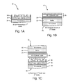
- FIGS. 1A-1E are cross-sectional views illustrating fabrication of an photonic integrated circuit (PIC) via heterogeneous integration of a III-V type semiconductor epitaxial layer deposited on a semiconductor wafer, and bonded to another semiconductor wafer according to an embodiment of the present invention.
- FIG. 1A illustrates fabrication of first wafer 10 , which includes a patterned silicon layer formed on a semiconductor substrate.
- FIG. 1B illustrates fabrication of a second wafer 12 that includes III-V type semiconductor epitaxial layer deposited on a semiconductor substrate.
- FIG. 1C illustrates bonding of first wafer 10 with second wafer 12 , and in particular to bonding of the III-V type semiconductor epitaxial layer of second wafer 12 to the patterned silicon layer of first wafer 10 .
- FIG. 1A illustrates fabrication of first wafer 10 , which includes a patterned silicon layer formed on a semiconductor substrate.
- FIG. 1B illustrates fabrication of a second wafer 12 that includes III-V type semiconductor epitaxial layer deposited on
- FIG. 1D illustrates reclamation of the semiconductor substrate associated with second wafer 12
- FIG. 1E illustrates processing of III-V type semiconductor epitaxial layer from second wafer 12 to define one or more active, optoelectronic devices (e.g., lasers, photodetectors, light-emitting diodes, etc.).
- the semiconductor substrates associated with first and second wafers are silicon (Si) substrates, selected for the low-cost associated with fabrication.
- FIGS. 1A-1E illustrate fabrication of active photonic integrated circuits (PICs) capable of taking advantage of the low-cost associated with silicon substrates.
- PICs active photonic integrated circuits
- first wafer 10 is fabricated to include silicon substrate 14 , buried oxide layer (BOX) 16 , and patterned silicon layer 18 .
- the embodiment shown in FIG. 1A is referred to as a silicon-on-insulator PIC, wherein silicon layer 18 is patterned as desired to form passive optical devices such waveguides, filters, splitters, etc. in addition to or in conjunction with non-optical devices.
- the embodiment shown in FIG. 1A may include passive waveguides, wherein light is carried in a core made of pure single-crystal silicon, typically formed in the active region of a silicon-on-insulator (SOI) wafer.
- SOI silicon-on-insulator
- passive devices such as waveguides may utilize dielectric waveguides to carry light in a central core made of an amorphous dielectric material, such as silicon nitride or silicon dioxide, which may not require a silicon-on-insulator (SOI) wafer.
- amorphous dielectric material such as silicon nitride or silicon dioxide
- SOI silicon-on-insulator
- Embodiments of the present invention may utilize either of these silicon-based photonic integrated circuits, or other well-known silicon-based photonic configurations.
- first wafer 10 with its silicon substrate—may be fabricated as a 300 millimeter (mm) diameter wafer, a 450 mm diameter wafer, or larger if available.
- mm millimeter
- PICs photonic integrated circuits
- second wafer 12 similarly includes silicon substrate 20 , buffer layer 22 , release layer 24 , and III-V type semiconductor epitaxial layer 26 (referred to herein as III-V epitaxial layer 26 ).
- III-V epitaxial layer 26 III-V type semiconductor epitaxial layer 26 Due to lattice constant differences between materials of different type such as silicon and III-V type materials, attempts to grow III-V type semiconductor layers directly on silicon typically results in a substantial number of defects which significantly degrades material quality and subsequent performance of processed devices. As a result, III-V epitaxial layers are typically grown on a substrate native to its material group (e.g., a III-V substrate as opposed to a silicon substrate). However, III-V type wafers are significantly more expensive than silicon wafers, and are not typically available on the same scale (e.g., 300-450 mm) as silicon wafers.
- the present invention utilizes buffer layer 22 between silicon substrate 20 and III-V epitaxial layer 26 to accommodate the lattice constant differences.
- silicon substrate 20 is fabricated as a wafer having a diameter equal to the diameter of first wafer 10 shown in FIG. 1A (e.g., 300-450 mm).
- Buffer layer 22 is deposited on silicon substrate 20 , and may include Germanium (Ge), Silicon Germanium (SiGe), Strontium Titanate (SrTO 3 ), Silicon dioxide (SiO 2 ), as well as combinations of one or more of these materials.
- the III-V epitaxial layer 26 is grown/deposited on buffer layer 22 .
- Epitaxial layer 26 may be comprised of a stack of layers grown/deposited via one or more of Molecular-Beam Epitaxy (MBE), Metal-Organic Chemical Vapor Deposition (MOCVD), Metal-Organic Vapor Phase Epitaxy (MOVPE), Hydride Vapor Phase Epitaxy (HVPE), and/or other well understood crystal growth processes.
- MBE Molecular-Beam Epitaxy
- MOCVD Metal-Organic Chemical Vapor Deposition
- MOVPE Metal-Organic Vapor Phase Epitaxy
- HVPE Hydride Vapor Phase Epitaxy
- III-V epitaxial layer 26 includes heterostructures with quantum dots grown in conjunction with wider band semiconductors.
- quantum dots comprised of Indium Arsenide (InAs) may be clad or surrounded by Aluminum Gallium Arsenide (Al x Ga y As) layers.
- InAs Indium Arsenide
- Al x Ga y As Aluminum Gallium Arsenide
- other configurations and materials may be utilized to form III-V epitaxial layer 26 such as those disclosed in U.S. Pat. No. 7,732,237 titled “Quantum Dot Based Optoelectronic Device and Method of Making Same”, by Ya-Hong Xie, incorporated by reference herein.
- other quantum structures may be utilized as part of III-V epitaxial layer 26 , including quantum dots, quantum wells, quantum wires, quantum dashes.
- first wafer 10 (shown in FIG. 1A ) has been fabricated and partially or completely processed.
- Second wafer 12 (shown in FIG. 1B ) has been fabricated to include III-V epitaxial layer 26 on silicon substrate 20 , but epitaxial layer 26 remains unprocessed. Because both first wafer 10 and second wafer 12 utilized silicon substrates, both can be fabricated on a scale commonly available for fabrication of silicon wafers (e.g., 300 mm-450 mm diameter wafer). As a result of each wafer being the same size, the respective wafers can be bonded to one another, as shown at FIG. 1C .
- III-V epitaxial layer 26 is unprocessed (i.e., no devices have yet been formed within III-V epitaxial layer 26 ), the alignment between the respective wafers can be relatively coarse.
- each surface should be sufficiently smoothed/polished to allow a good bond to be formed.
- a chemical-mechanical polish (CMP) step may be utilized on one or both surfaces prior to bonding the two wafers.
- second wafer 12 is flipped such that III-V epitaxial layer 26 is oriented to face patterned silicon layer 18 .
- the respective wafers are bonded together using one or more bonding processes, such as hydrophilic, hydrophobic, plasma assisted, solder/metal, and/or polymer (e.g., benzocyclobutene (BCB)) bonding.
- bonding processes such as hydrophilic, hydrophobic, plasma assisted, solder/metal, and/or polymer (e.g., benzocyclobutene (BCB)) bonding.
- BCB benzocyclobutene
- One of the benefits of the present invention is that both first wafer 10 and second wafer 12 are based on silicon substrates, and therefore share the same coefficient of expansion.
- the bonding process may take advantage of high-temperature annealing processes to form the desired mechanical bond between the respective wafers.
- III-V epitaxial layer 26 has not yet been processed, alignment of the III-V epitaxial layer 26 with patterned silicon layer 18 does not require specific or precise alignment between the respective wafers. Rather, only the subsequent processing of the III-V epitaxial layer 26 need be precise. Because III-V epitaxial layer 26 is bonded directly to patterned silicon layer 18 , optical coupling between active optoelectronic devices subsequently formed in III-V epitaxial layer 26 and passive opto-electronic devices formed in patterned silicon layer 18 is straightforward that is, does not require light to pass through intermediate layers for coupling between the respective optical devices.
- some embodiments may require electrical conductivity between patterned silicon layer 18 and optoelectronic devices subsequently formed in III-V epitaxial layer 26 .
- first wafer 10 and second wafer 12 utilize a silicon substrate resulting in similar coefficients of expansion between the respective wafers a high-temperature bonding and annealing process can be utilized to provide electrical conductivity between the respective wafers.
- this type of electrical conductivity between bonded wafers requires metal contact pads associated with each wafer or individual device to be aligned prior to soldering or otherwise forming an electrical contact between the respective contact pads.
- release layer 24 is positioned between buffer layer 22 and III-V epitaxial layer 26 , and is selectively etched away as shown in FIG. 1D to separate buffer layer 22 and silicon substrate 20 from III-V epitaxial layer 26 .
- release layer 24 is comprised of Aluminum Arsenide (AlAs), and can be selectively etched via hydrofluoric acid (HF), without damaging or otherwise removing III-V epitaxy layer 26 .
- both the growth substrate 20 and buffer layer 22 are etched and/or mechanically lapped and then the remaining ⁇ 10 s microns of Si can be selectively etched.
- III-V epitaxial layer 26 is exposed to allow for subsequent processing of the III-V epitaxial layer.
- III-V epitaxial layer 26 is processed to create the desired active optoelectronic devices, such as lasers, photodetectors, light-emitting diodes, etc.
- the completed photonic integrated circuit includes silicon substrate 14 , buried oxide layer (BOX) 16 , patterned silicon layer 18 , patterned III-V epitaxial layer 26 , which in this embodiment includes III-V type semiconductor spacer layer 30 , III-V type semiconductor quantum structure layer 32 , contacts 34 , bulk semiconductor layer 36 , insulator material 38 , and contact 40 .
- Gaps 42 may be air gaps (as shown in FIG. 1E ), or may utilize one or more materials to form the desired waveguide, such as silicon oxide, silicon oxynitride, silicon nitride, etc.
- the shape of gaps 42 may be linear (in a direction into the page) or in the form of others shapes such as bends, rings, and/or discs depending on the function of the particular waveguide.
- the combination of III-V spacer layer 36 , III-V quantum structure layer 32 , contacts 34 and 40 and bulk semiconductor layer 36 form an optically active region that may be incorporated into devices such as light emitting diodes, laser diodes, photodetectors, modulators, phase tuning elements, interferometric devices, wavelength multiplexers, polarization splitters, couplers, and/or saturable absorbers.
- the active optoelectronic devices found within III-V epitaxial layer 26 are optically coupled to passive optical devices (e.g., waveguides) formed in patterned silicon layer 18 associated with first wafer 10 .
- bonding of the first wafer and second wafer includes electrically coupling patterned silicon layer 18 (or metal contacts formed thereon) with active optoelectronic devices formed in III-V epitaxial layer 26 .
- Benefits of the embodiment shown in FIGS. 1A-1E include the ability to utilize wafers with silicon substrates as opposed to the more expensive III-V type substrates. As a result of both wafers utilizing the same substrate material and therefore sharing the same coefficient of thermal expansion the wafers can be bonded together using high temperature bonding/annealing processes. Finally, the III-V epitaxial layer 26 is not processed until after the wafers have been bonded. As a result, bonding of the wafers does not require precise alignment of the wafers as is required when bonding a processed device to a wafer.
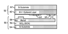
- FIGS. 2A-2B are cross-sectional views illustrating in additional detail the bonding of first wafer 50 to second wafer 52 according to an embodiment of the present invention, wherein the second wafer once again includes a III-V type semiconductor epitaxial layer formed on a silicon substrate.
- the embodiment shown in FIGS. 2A-2B illustrates the capability of bonding between semiconductor material (such as III-V type semiconductor material) and metal.
- semiconductor material such as III-V type semiconductor material
- metal electrical coupling or conductivity paths can be created between first wafer 50 and second wafer 52 , in addition to optical coupling described with respect to FIGS. 1A-1E .
- mechanical bonding is done between semiconductors, and electrical bonding is done between respective metal contacts.
- first wafer 50 includes silicon substrate 54 , buried silicon dioxide layer (SiO 2 ) 56 , and metal layer 58 .
- second wafer 52 includes III-V epitaxial layer 60 and silicon growth substrate 62 .
- the embodiment shown in FIG. 2A-2B may be utilized in conjunction with the fabrication steps described with respect to FIGS. 1A-1E .
- Typical bonding between devices requires alignment between metal contacts fabricated on each processed device, which again requires precise alignment between the respective devices. Because the present invention takes advantage of bonding the III-V epitaxial layer to the patterned silicon substrate, precise alignment is not required.
- first wafer 50 is bonded to second wafer 52 .
- the bonding process utilizes one or more well-known bonding techniques such as plasma-assisted bonding, followed by an anneal process under pressure.
- the bonding may utilize bonding techniques such as plasma-assisted bonding combined with annealing under pressure to form the requisite mechanical bond between the respective wafers.
- covalent bonds are formed between silicon dioxide layer 56 and III-V epitaxial layer 60 .
- metal layer 58 includes thin contact portion 64 located on a surface of first wafer exposed to bonding with second wafer 52 .
- Thin contact portion 64 may be formed within silicon dioxide layer 56 such that at least a small portion of thin contact portion 64 extends beyond the silicon dioxide layer 56 .
- Thin metal contact portion 64 will both expand and then contract during heating and cooling associated with the bonding/annealing process, resulting in small areas surrounding each thin metal contact portion 64 that is not bonded to III-V epitaxial layer 60 .
- the net result of this process is that bonding via covalent bonds is provided between semiconductor materials and bonding via interdiffusion is provided between metal contacts and a semiconductor material such as III-V epitaxial layer 60 to provide both a mechanical and electrical bond between the respective first and second wafers.
- metal layer 58 may also extend to silicon substrate 54 , and contacts may be included therein to allow an electrical connection to be formed between first wafer 50 and an external device.
Landscapes
- Physics & Mathematics (AREA)
- Engineering & Computer Science (AREA)
- Microelectronics & Electronic Packaging (AREA)
- General Physics & Mathematics (AREA)
- Optics & Photonics (AREA)
- Semiconductor Lasers (AREA)
- Recrystallisation Techniques (AREA)
- Light Receiving Elements (AREA)
Abstract
Description
- This application claims priority to U.S. Provisional Application No. 61/919,417, titled “Bonding of Heterogeneous Material Grown on Silicon to Silicon Photonic Circuits” and filed on Dec. 20, 2013, which is incorporated herein by reference. A claim of priority is made.
- This invention was made with Government support under contract number HR0011-12-C-0006 awarded by the Defense Advanced Research Projects Agency. The Government has certain rights in this invention.
- The present disclosure relates to integrated circuit fabrication, and in particular to fabrication of optoelectronic integrated circuits.
- Data communication or “Datacom” has traditionally relied on copper wires to transmit data from point to point. For example, a copper communication bus may provide communication between a processor and a data storage medium in a household PC, or between servers in a data center. Communication via a traditional copper communication bus is well understood and benefits from the fact that both the endpoint and communication medium are electrical devices.
- Optical communication systems offer the promise of greater bandwidth and speed. However, optical communication systems suffer from the interface required between the optical communication system and electrical devices. In particular, coupling of optical components and electrical components typically results in electrical and optical coupling losses and/or signal distortions. These and other obstacles have been addressed by integrating the optical devices onto the integrated circuits in what is referred to as a Photonic Integrated Circuit (PIC). That is, the optical components/devices are created on semiconductor substrates that allow for integration with traditional semiconductor devices.
- The semiconductor material silicon (Si) has been the backbone of integrated circuit technology for many years. However, due to the indirect bandgap of silicon—which complicates the production of light—fabrication of active optoelectronic devices has relied on a different class of semiconductor material referred to herein as III-V type semiconductors. These semiconductor materials include combinations of group III elements Aluminum (Al), Gallium (Ga), Indium (In) with group V elements Nitrogen (N), Phosphorus (P), Arsenic (As), and Antimony (Sb), and include combinations such as Gallium Arsenide (GaAs), Indium Phosphide (InP), Gallium Phosphide (GaP), Gallium Nitride (GaN), and Aluminum Gallium Arsenide (AlGaAs). A characteristic of III-V type semiconductors is the direct band gap, which allows for the fabrication of active optoelectronic devices such as lasers, photodetectors, and light-emitting diodes.
- Conventional methods for integrating III-V type semiconductors with traditional silicon integrated circuits have tended to follow two approaches. In the first approach, III-V type semiconductor material is deposited directly on a silicon substrate or processed silicon layer. However, lattice constant differences between silicon and III-V type semiconductor materials results in fatal defects (e.g., dislocations) near the silicon/III-V interface. To overcome these defects, a buffer layer can be deposited between the silicon/III-V interface. However, while progress has been made to decrease the thickness of the buffer layer, thin layers can still represent a source of random, lossy defects that negatively impacts coupling between the active III-V devices and the passive silicon components (e.g., electrical circuits, waveguides, etc.). In the second approach, III-V type semiconductor material is grown on a native III-V type substrate having the same or similar lattice constant and then transferred to a silicon substrate. However, this approach is costly as the cost of producing III-V type semiconductor substrates is far greater than the cost of producing a silicon substrate. In addition, placement of the processed, active III-V device requires precise alignment between the device and the passive component (e.g., waveguide, etc.) to which it is coupled.
- According to one embodiment of the present invention, a method of fabricating a heterogeneous semiconductor wafer is described that includes depositing a III-V type semiconductor epitaxial layer on a first wafer having a semiconductor substrate. The first wafer is then bonded to a second wafer having a patterned silicon layer formed on a semiconductor substrate, wherein the III-V type semiconductor epitaxial layer is bonded to the patterned silicon layer of the second wafer. The semiconductor substrate associated with the first wafer is removed to expose the III-V type semiconductor epitaxial layer.
- According to another embodiment, a heterogeneous wafer includes a first wafer and a second wafer. The first wafer is comprised of a semiconductor substrate and a patterned silicon layer, wherein the patterned silicon layer is formed on the semiconductor substrate. The second wafer is comprised of a semiconductor substrate and a III-V type semiconductor epitaxial layer. The second wafer is bonded to the first wafer such that the III-V type semiconductor epitaxial layer is bonded to the patterned silicon layer.
-
FIGS. 1A-1E are cross-sectional views illustrating fabrication of a photonic integrated circuit via heterogeneous integration of a III-V type semiconductor epitaxy deposited on a silicon wafer and bonded to another silicon substrate wafer according to an embodiment of the present invention. -
FIGS. 2A-2B are cross-sectional views illustrating in additional detail the bonding of a wafer having a silicon substrate and a III-V epitaxial layer with another silicon wafer according to an embodiment of the present invention. - The present disclosure is directed generally to the fabrication of photonic integrated circuits (PICs), and in particular to methods that allow PICs to be fabricated on a cost-effective scale. The fabrication process deposits a III-V type semiconductor epitaxial layer on a silicon growth substrate, which allows the wafer to be scaled to the same size as traditional silicon wafers (e.g., 300-450 mm diameters). The III-V type semiconductor epitaxial layer is then bonded to a patterned silicon wafer in a wafer-to-wafer bonding procedure. After bonding, the silicon growth substrate is removed or reclaimed, leaving exposed for subsequent processing the III-V type semiconductor epitaxial layer. Processing of the III-V type epitaxial layer allows individual and potentially diverse active optoelectronic devices to be defined and coupled to the previously patterned silicon wafer to which the III-V epitaxy layer is bonded.
- This method of fabrication is in contrast to typical coupling of III-V type semiconductor devices with silicon wafers in which III-V type semiconductor devices not wafers are individually bonded to a patterned silicon wafer. Not only does this process require precise alignment between the optoelectronic device and the processed silicon wafer but also typically relies on fabrication of the III-V optoelectronic device on III-V type substrates, which are many times as expensive to fabrication as silicon wafers.
-
FIGS. 1A-1E are cross-sectional views illustrating fabrication of an photonic integrated circuit (PIC) via heterogeneous integration of a III-V type semiconductor epitaxial layer deposited on a semiconductor wafer, and bonded to another semiconductor wafer according to an embodiment of the present invention. In particular,FIG. 1A illustrates fabrication offirst wafer 10, which includes a patterned silicon layer formed on a semiconductor substrate.FIG. 1B illustrates fabrication of asecond wafer 12 that includes III-V type semiconductor epitaxial layer deposited on a semiconductor substrate.FIG. 1C illustrates bonding offirst wafer 10 withsecond wafer 12, and in particular to bonding of the III-V type semiconductor epitaxial layer ofsecond wafer 12 to the patterned silicon layer offirst wafer 10.FIG. 1D illustrates reclamation of the semiconductor substrate associated withsecond wafer 12, andFIG. 1E illustrates processing of III-V type semiconductor epitaxial layer fromsecond wafer 12 to define one or more active, optoelectronic devices (e.g., lasers, photodetectors, light-emitting diodes, etc.). In the embodiments shown inFIGS. 1A-1E , the semiconductor substrates associated with first and second wafers are silicon (Si) substrates, selected for the low-cost associated with fabrication. The embodiments shown inFIGS. 1A-1E illustrate fabrication of active photonic integrated circuits (PICs) capable of taking advantage of the low-cost associated with silicon substrates. However, it should be understood that other type of semiconductor substrates may be utilized if so desired. - At the fabrication stage shown in
FIG. 1A ,first wafer 10 is fabricated to includesilicon substrate 14, buried oxide layer (BOX) 16, and patternedsilicon layer 18. The embodiment shown inFIG. 1A is referred to as a silicon-on-insulator PIC, whereinsilicon layer 18 is patterned as desired to form passive optical devices such waveguides, filters, splitters, etc. in addition to or in conjunction with non-optical devices. For example, the embodiment shown inFIG. 1A may include passive waveguides, wherein light is carried in a core made of pure single-crystal silicon, typically formed in the active region of a silicon-on-insulator (SOI) wafer. However, in other embodiments, passive devices such as waveguides may utilize dielectric waveguides to carry light in a central core made of an amorphous dielectric material, such as silicon nitride or silicon dioxide, which may not require a silicon-on-insulator (SOI) wafer. Embodiments of the present invention may utilize either of these silicon-based photonic integrated circuits, or other well-known silicon-based photonic configurations. - A benefit of silicon-based PICs is that fabrication and processing is conducted via standard and well understood CMOS technology, thereby enabling mass-fabrication and cost reduction due to economies of scale. For example,
first wafer 10—with its silicon substrate—may be fabricated as a 300 millimeter (mm) diameter wafer, a 450 mm diameter wafer, or larger if available. Although a silicon-on-insulator type device is illustrated in the embodiment shown inFIG. 1A , other types of silicon based photonic integrated circuits (PICs) may be utilized according to embodiments of the present invention. - At the fabrication stage shown in
FIG. 1B ,second wafer 12 similarly includessilicon substrate 20,buffer layer 22,release layer 24, and III-V type semiconductor epitaxial layer 26 (referred to herein as III-V epitaxial layer 26). Due to lattice constant differences between materials of different type such as silicon and III-V type materials, attempts to grow III-V type semiconductor layers directly on silicon typically results in a substantial number of defects which significantly degrades material quality and subsequent performance of processed devices. As a result, III-V epitaxial layers are typically grown on a substrate native to its material group (e.g., a III-V substrate as opposed to a silicon substrate). However, III-V type wafers are significantly more expensive than silicon wafers, and are not typically available on the same scale (e.g., 300-450 mm) as silicon wafers. - To overcome these issues, the present invention utilizes
buffer layer 22 betweensilicon substrate 20 and III-V epitaxial layer 26 to accommodate the lattice constant differences. In the embodiment shown inFIG. 1B ,silicon substrate 20 is fabricated as a wafer having a diameter equal to the diameter offirst wafer 10 shown inFIG. 1A (e.g., 300-450 mm).Buffer layer 22 is deposited onsilicon substrate 20, and may include Germanium (Ge), Silicon Germanium (SiGe), Strontium Titanate (SrTO3), Silicon dioxide (SiO2), as well as combinations of one or more of these materials. It should be understood that this list is not exhaustive, and that other such materials may be used to bridge the lattice constant difference ofsilicon substrate 20 and the III-V epitaxial layer 26. Further, the selection of materials forbuffer layer 22 is dependent on the selection of material for III-V epitaxial layer 26, in order to reduce the strain betweensilicon substrate 20 and III-V epitaxial layer 26. - In the embodiment shown in
FIG. 1B , having depositedbuffer layer 22 onsilicon substrate 20, the III-V epitaxial layer 26 is grown/deposited onbuffer layer 22.Epitaxial layer 26 may be comprised of a stack of layers grown/deposited via one or more of Molecular-Beam Epitaxy (MBE), Metal-Organic Chemical Vapor Deposition (MOCVD), Metal-Organic Vapor Phase Epitaxy (MOVPE), Hydride Vapor Phase Epitaxy (HVPE), and/or other well understood crystal growth processes. In one embodiment, III-V epitaxial layer 26 includes heterostructures with quantum dots grown in conjunction with wider band semiconductors. For example, quantum dots comprised of Indium Arsenide (InAs) may be clad or surrounded by Aluminum Gallium Arsenide (AlxGayAs) layers. In other embodiments, other configurations and materials may be utilized to form III-V epitaxial layer 26 such as those disclosed in U.S. Pat. No. 7,732,237 titled “Quantum Dot Based Optoelectronic Device and Method of Making Same”, by Ya-Hong Xie, incorporated by reference herein. In other embodiments, other quantum structures may be utilized as part of III-V epitaxial layer 26, including quantum dots, quantum wells, quantum wires, quantum dashes. - At this stage in the fabrication process, first wafer 10 (shown in
FIG. 1A ) has been fabricated and partially or completely processed. Second wafer 12 (shown inFIG. 1B ) has been fabricated to include III-V epitaxial layer 26 onsilicon substrate 20, butepitaxial layer 26 remains unprocessed. Because bothfirst wafer 10 andsecond wafer 12 utilized silicon substrates, both can be fabricated on a scale commonly available for fabrication of silicon wafers (e.g., 300 mm-450 mm diameter wafer). As a result of each wafer being the same size, the respective wafers can be bonded to one another, as shown atFIG. 1C . In addition, because III-V epitaxial layer 26 is unprocessed (i.e., no devices have yet been formed within III-V epitaxial layer 26), the alignment between the respective wafers can be relatively coarse. Prior to bonding, however, the respective surfaces to be bond together—patternedsilicon layer 18 onfirst wafer 10 and III-V epitaxial layer 24 onsecond wafer 12—must be properly prepared. For example, each surface should be sufficiently smoothed/polished to allow a good bond to be formed. For example, a chemical-mechanical polish (CMP) step may be utilized on one or both surfaces prior to bonding the two wafers. - In the embodiment shown in
FIG. 1C ,second wafer 12 is flipped such that III-V epitaxial layer 26 is oriented to face patternedsilicon layer 18. The respective wafers are bonded together using one or more bonding processes, such as hydrophilic, hydrophobic, plasma assisted, solder/metal, and/or polymer (e.g., benzocyclobutene (BCB)) bonding. One of the benefits of the present invention, however, is that bothfirst wafer 10 andsecond wafer 12 are based on silicon substrates, and therefore share the same coefficient of expansion. As a result, the bonding process may take advantage of high-temperature annealing processes to form the desired mechanical bond between the respective wafers. In addition, because the III-V epitaxial layer 26 has not yet been processed, alignment of the III-V epitaxial layer 26 with patternedsilicon layer 18 does not require specific or precise alignment between the respective wafers. Rather, only the subsequent processing of the III-V epitaxial layer 26 need be precise. Because III-V epitaxial layer 26 is bonded directly to patternedsilicon layer 18, optical coupling between active optoelectronic devices subsequently formed in III-V epitaxial layer 26 and passive opto-electronic devices formed in patternedsilicon layer 18 is straightforward that is, does not require light to pass through intermediate layers for coupling between the respective optical devices. - As described in more detail with respect to
FIGS. 2A-2B , some embodiments may require electrical conductivity between patternedsilicon layer 18 and optoelectronic devices subsequently formed in III-V epitaxial layer 26. Because bothfirst wafer 10 andsecond wafer 12 utilize a silicon substrate resulting in similar coefficients of expansion between the respective wafers a high-temperature bonding and annealing process can be utilized to provide electrical conductivity between the respective wafers. Typically, this type of electrical conductivity between bonded wafers requires metal contact pads associated with each wafer or individual device to be aligned prior to soldering or otherwise forming an electrical contact between the respective contact pads. - Following bonding of the respective wafers as shown in
FIG. 1C , in the fabrication step shown inFIG. 1D ,silicon substrate 20 associated withsecond wafer 10 is reclaimed for subsequent use. In the embodiment shown inFIG. 1D ,release layer 24 is positioned betweenbuffer layer 22 and III-V epitaxial layer 26, and is selectively etched away as shown inFIG. 1D to separatebuffer layer 22 andsilicon substrate 20 from III-V epitaxial layer 26. For example, in one embodiment,release layer 24 is comprised of Aluminum Arsenide (AlAs), and can be selectively etched via hydrofluoric acid (HF), without damaging or otherwise removing III-V epitaxy layer 26. In another embodiment (not shown), rather than attempt to reclaimsilicon growth substrate 20, both thegrowth substrate 20 andbuffer layer 22 are etched and/or mechanically lapped and then the remaining ˜10 s microns of Si can be selectively etched. At the end of this fabrication step, III-V epitaxial layer 26 is exposed to allow for subsequent processing of the III-V epitaxial layer. - At the fabrication step shown in
FIG. 1E , III-V epitaxial layer 26 is processed to create the desired active optoelectronic devices, such as lasers, photodetectors, light-emitting diodes, etc. In the embodiment shown inFIG. 1E , the completed photonic integrated circuit includessilicon substrate 14, buried oxide layer (BOX) 16, patternedsilicon layer 18, patterned III-V epitaxial layer 26, which in this embodiment includes III-V typesemiconductor spacer layer 30, III-V type semiconductorquantum structure layer 32,contacts 34,bulk semiconductor layer 36,insulator material 38, andcontact 40. - In addition, the bonding of patterned
silicon layer 18 to III-Vtype epitaxial layer 26 results in the creation of a number ofgaps 42 within the patterned silicon layer that in this embodiment serve as waveguides for light created by the active regions within the III-Vtype epitaxial layer 26.Gaps 42 may be air gaps (as shown inFIG. 1E ), or may utilize one or more materials to form the desired waveguide, such as silicon oxide, silicon oxynitride, silicon nitride, etc. In addition, the shape ofgaps 42 may be linear (in a direction into the page) or in the form of others shapes such as bends, rings, and/or discs depending on the function of the particular waveguide. - In the embodiment shown in
FIG. 1E , the combination of III-V spacer layer 36, III-Vquantum structure layer 32,contacts bulk semiconductor layer 36 form an optically active region that may be incorporated into devices such as light emitting diodes, laser diodes, photodetectors, modulators, phase tuning elements, interferometric devices, wavelength multiplexers, polarization splitters, couplers, and/or saturable absorbers. In some embodiments, the active optoelectronic devices found within III-V epitaxial layer 26 are optically coupled to passive optical devices (e.g., waveguides) formed in patternedsilicon layer 18 associated withfirst wafer 10. However, while optical coupling is possible in other embodiments, no coupling is required between patternedsilicon layer 18 and devices formed in III-V epitaxial layer 26. In still other embodiments such as that shown inFIGS. 2A-2B , bonding of the first wafer and second wafer includes electrically coupling patterned silicon layer 18 (or metal contacts formed thereon) with active optoelectronic devices formed in III-V epitaxial layer 26. - Benefits of the embodiment shown in
FIGS. 1A-1E include the ability to utilize wafers with silicon substrates as opposed to the more expensive III-V type substrates. As a result of both wafers utilizing the same substrate material and therefore sharing the same coefficient of thermal expansion the wafers can be bonded together using high temperature bonding/annealing processes. Finally, the III-V epitaxial layer 26 is not processed until after the wafers have been bonded. As a result, bonding of the wafers does not require precise alignment of the wafers as is required when bonding a processed device to a wafer. -
FIGS. 2A-2B are cross-sectional views illustrating in additional detail the bonding offirst wafer 50 tosecond wafer 52 according to an embodiment of the present invention, wherein the second wafer once again includes a III-V type semiconductor epitaxial layer formed on a silicon substrate. In particular, the embodiment shown inFIGS. 2A-2B illustrates the capability of bonding between semiconductor material (such as III-V type semiconductor material) and metal. As a result, electrical coupling or conductivity paths can be created betweenfirst wafer 50 andsecond wafer 52, in addition to optical coupling described with respect toFIGS. 1A-1E . Typically, mechanical bonding is done between semiconductors, and electrical bonding is done between respective metal contacts. The embodiments shown inFIGS. 2A-2B provides for bonding between semiconductor and metal. In the embodiment shown inFIGS. 2A-2B ,first wafer 50 includessilicon substrate 54, buried silicon dioxide layer (SiO2) 56, andmetal layer 58. In addition,second wafer 52 includes III-V epitaxial layer 60 andsilicon growth substrate 62. The embodiment shown inFIG. 2A-2B may be utilized in conjunction with the fabrication steps described with respect toFIGS. 1A-1E . - Typical bonding between devices requires alignment between metal contacts fabricated on each processed device, which again requires precise alignment between the respective devices. Because the present invention takes advantage of bonding the III-V epitaxial layer to the patterned silicon substrate, precise alignment is not required.
- In the embodiment shown in
FIG. 2A ,first wafer 50 is bonded tosecond wafer 52. The bonding process utilizes one or more well-known bonding techniques such as plasma-assisted bonding, followed by an anneal process under pressure. The bonding may utilize bonding techniques such as plasma-assisted bonding combined with annealing under pressure to form the requisite mechanical bond between the respective wafers. As a result of this process, covalent bonds are formed betweensilicon dioxide layer 56 and III-V epitaxial layer 60. - In addition to the covalent bonds formed between the respective semiconductor materials of each wafer, a bond is also formed between
metal layer 58 and III-V epitaxial layer 60 to provide an electrically conductive coupling or path between the respective wafers. In particular, in the embodiment shown inFIGS. 2A-2B ,metal layer 58 includesthin contact portion 64 located on a surface of first wafer exposed to bonding withsecond wafer 52.Thin contact portion 64 may be formed withinsilicon dioxide layer 56 such that at least a small portion ofthin contact portion 64 extends beyond thesilicon dioxide layer 56. During the bonding and annealing process, interdiffusion occurs betweenthin contact portion 64 and III-V epitaxial layer 60 to form a bond between the two layers. Thinmetal contact portion 64 will both expand and then contract during heating and cooling associated with the bonding/annealing process, resulting in small areas surrounding each thinmetal contact portion 64 that is not bonded to III-V epitaxial layer 60. However, the net result of this process is that bonding via covalent bonds is provided between semiconductor materials and bonding via interdiffusion is provided between metal contacts and a semiconductor material such as III-V epitaxial layer 60 to provide both a mechanical and electrical bond between the respective first and second wafers. Although not shown inFIGS. 2A and 2B ,metal layer 58 may also extend tosilicon substrate 54, and contacts may be included therein to allow an electrical connection to be formed betweenfirst wafer 50 and an external device. - While the invention has been described with reference to an exemplary embodiment(s), it will be understood by those skilled in the art that various changes may be made and equivalents may be substituted for elements thereof without departing from the scope of the invention. In addition, many modifications may be made to adapt a particular situation or material to the teachings of the invention without departing from the essential scope thereof. Therefore, it is intended that the invention not be limited to the particular embodiment(s) disclosed, but that the invention will include all embodiments falling within the scope of the appended claims.
Claims (25)
Priority Applications (2)
| Application Number | Priority Date | Filing Date | Title |
|---|---|---|---|
| US14/577,938 US9360623B2 (en) | 2013-12-20 | 2014-12-19 | Bonding of heterogeneous material grown on silicon to a silicon photonic circuit |
| US15/172,963 US20170227708A1 (en) | 2013-12-20 | 2016-06-03 | Bonding of a heterogeneous material grown on silicon to a silicon photonic circuit |
Applications Claiming Priority (2)
| Application Number | Priority Date | Filing Date | Title |
|---|---|---|---|
| US201361919417P | 2013-12-20 | 2013-12-20 | |
| US14/577,938 US9360623B2 (en) | 2013-12-20 | 2014-12-19 | Bonding of heterogeneous material grown on silicon to a silicon photonic circuit |
Related Child Applications (1)
| Application Number | Title | Priority Date | Filing Date |
|---|---|---|---|
| US15/172,963 Division US20170227708A1 (en) | 2013-12-20 | 2016-06-03 | Bonding of a heterogeneous material grown on silicon to a silicon photonic circuit |
Publications (2)
| Publication Number | Publication Date |
|---|---|
| US20150177458A1 true US20150177458A1 (en) | 2015-06-25 |
| US9360623B2 US9360623B2 (en) | 2016-06-07 |
Family
ID=53399803
Family Applications (2)
| Application Number | Title | Priority Date | Filing Date |
|---|---|---|---|
| US14/577,938 Active US9360623B2 (en) | 2013-12-20 | 2014-12-19 | Bonding of heterogeneous material grown on silicon to a silicon photonic circuit |
| US15/172,963 Abandoned US20170227708A1 (en) | 2013-12-20 | 2016-06-03 | Bonding of a heterogeneous material grown on silicon to a silicon photonic circuit |
Family Applications After (1)
| Application Number | Title | Priority Date | Filing Date |
|---|---|---|---|
| US15/172,963 Abandoned US20170227708A1 (en) | 2013-12-20 | 2016-06-03 | Bonding of a heterogeneous material grown on silicon to a silicon photonic circuit |
Country Status (2)
| Country | Link |
|---|---|
| US (2) | US9360623B2 (en) |
| CN (1) | CN104882368B (en) |
Cited By (27)
| Publication number | Priority date | Publication date | Assignee | Title |
|---|---|---|---|---|
| US20160163917A1 (en) * | 2013-07-29 | 2016-06-09 | Epistar Corporation | Method of selectively transferring semiconductor device |
| US20170025377A1 (en) * | 2014-02-27 | 2017-01-26 | Commissariat à l'énergie atomique et aux énergies alternatives | Process for producing a structure by assembling at least two elements by direct adhesive bonding |
| US20170227709A1 (en) * | 2016-02-08 | 2017-08-10 | Skorpios Technologies, Inc. | Stepped optical bridge for connecting semiconductor waveguides |
| WO2017210534A1 (en) * | 2016-06-03 | 2017-12-07 | University Of Central Florida Research Foundation, Inc. | Hetero-structure-based integrated photonic devices, methods and applications |
| US10109983B2 (en) | 2016-04-28 | 2018-10-23 | Hewlett Packard Enterprise Development Lp | Devices with quantum dots |
| US10366883B2 (en) | 2014-07-30 | 2019-07-30 | Hewlett Packard Enterprise Development Lp | Hybrid multilayer device |
| US10381801B1 (en) | 2018-04-26 | 2019-08-13 | Hewlett Packard Enterprise Development Lp | Device including structure over airgap |
| US10396521B2 (en) | 2017-09-29 | 2019-08-27 | Hewlett Packard Enterprise Development Lp | Laser |
| US20190273356A1 (en) * | 2018-03-02 | 2019-09-05 | Cisco Technology, Inc. | Silicon photonics co-integrated with quantum dot lasers on silicon |
| WO2019169318A1 (en) * | 2018-03-02 | 2019-09-06 | Cisco Technology, Inc. | Quantum dot lasers integrated on silicon submount with mechanical features and through-silicon vias |
| US10461495B2 (en) | 2018-03-02 | 2019-10-29 | Cisco Technology, Inc. | Substrate technology for quantum dot lasers integrated on silicon |
| US10509163B2 (en) | 2016-02-08 | 2019-12-17 | Skorpios Technologies, Inc. | High-speed optical transmitter with a silicon substrate |
| US10566765B2 (en) | 2016-10-27 | 2020-02-18 | Hewlett Packard Enterprise Development Lp | Multi-wavelength semiconductor lasers |
| US10586847B2 (en) * | 2016-01-15 | 2020-03-10 | Hewlett Packard Enterprise Development Lp | Multilayer device |
| US10658177B2 (en) | 2015-09-03 | 2020-05-19 | Hewlett Packard Enterprise Development Lp | Defect-free heterogeneous substrates |
| WO2020106359A1 (en) * | 2018-11-21 | 2020-05-28 | The Research Foundation For The State University Of New York | Photonics optoelectrical system |
| US10680407B2 (en) | 2017-04-10 | 2020-06-09 | Hewlett Packard Enterprise Development Lp | Multi-wavelength semiconductor comb lasers |
| US10732349B2 (en) | 2016-02-08 | 2020-08-04 | Skorpios Technologies, Inc. | Broadband back mirror for a III-V chip in silicon photonics |
| US10734788B2 (en) * | 2018-03-02 | 2020-08-04 | Cisco Technology, Inc. | Quantum dot lasers integrated on silicon submount with mechanical features and through-silicon vias |
| US10928588B2 (en) | 2017-10-13 | 2021-02-23 | Skorpios Technologies, Inc. | Transceiver module for optical communication |
| US10935722B1 (en) * | 2019-09-14 | 2021-03-02 | Dong Li | CMOS compatible material platform for photonic integrated circuits |
| US11029466B2 (en) | 2018-11-21 | 2021-06-08 | The Research Foundation For The State University Of New York | Photonics structure with integrated laser |
| US11081620B2 (en) | 2016-12-16 | 2021-08-03 | Osram Oled Gmbh | Method of producing a semiconductor component |
| US11088244B2 (en) | 2016-03-30 | 2021-08-10 | Hewlett Packard Enterprise Development Lp | Devices having substrates with selective airgap regions |
| US11742451B2 (en) | 2020-11-24 | 2023-08-29 | Cisco Technology, Inc. | Integrate stressor with Ge photodiode using a substrate removal process |
| US11804525B2 (en) * | 2019-10-11 | 2023-10-31 | The Regents Of The University Of California | Dislocation glide suppression for misfit dislocation free heteroepitaxy |
| US11971575B2 (en) * | 2020-06-30 | 2024-04-30 | Openlight Photonics, Inc. | Integrated bandgap temperature sensor |
Families Citing this family (11)
| Publication number | Priority date | Publication date | Assignee | Title |
|---|---|---|---|---|
| CN105676368A (en) * | 2016-03-18 | 2016-06-15 | 中国电子科技集团公司第五十五研究所 | Method for manufacturing silicon-based micro ring filter and indium phosphide-based photo-detector heterogeneous integrated monochip |
| CN107046228B (en) * | 2017-04-07 | 2019-08-06 | 华南师范大学 | A kind of Electroabsorption Modulated Laser and preparation method thereof |
| CN109686658B (en) * | 2018-12-13 | 2021-03-09 | 中国科学院微电子研究所 | Semiconductor device and method for manufacturing the same |
| CN110518032B (en) * | 2019-09-02 | 2022-12-23 | 电子科技大学 | Polycrystalline silicon SOI substrate type photoelectric coupler, integrated circuit thereof and preparation method |
| CN110491967B (en) * | 2019-09-02 | 2021-03-02 | 电子科技大学 | Reverse bias type silicon light-emitting SOI photoelectric isolator, integrated circuit thereof and manufacturing method |
| CN110854017B (en) * | 2019-11-22 | 2022-07-12 | 中国科学院微电子研究所 | Integration method of germanium-based detector |
| US11340512B2 (en) * | 2020-04-27 | 2022-05-24 | Raytheon Bbn Technologies Corp. | Integration of electronics with Lithium Niobate photonics |
| CN112652676A (en) * | 2020-12-02 | 2021-04-13 | 广东省大湾区集成电路与系统应用研究院 | Integration structure and integration method of detector |
| CN112713215A (en) * | 2020-12-03 | 2021-04-27 | 广东省大湾区集成电路与系统应用研究院 | Integration structure and integration method of detector |
| CN115881555A (en) * | 2022-12-23 | 2023-03-31 | 杰创半导体(苏州)有限公司 | Manufacturing method of semiconductor device and semiconductor device structure |
| CN116314169B (en) * | 2023-05-23 | 2023-08-11 | 之江实验室 | Packaging structure of silicon-based integrated light receiving chip |
Citations (11)
| Publication number | Priority date | Publication date | Assignee | Title |
|---|---|---|---|---|
| US20020009612A1 (en) * | 2000-07-24 | 2002-01-24 | Motorola, Inc. | Microelectronic piezoelectric structure and method of forming the same |
| US6962835B2 (en) * | 2003-02-07 | 2005-11-08 | Ziptronix, Inc. | Method for room temperature metal direct bonding |
| US20060281203A1 (en) * | 2005-06-09 | 2006-12-14 | Lumileds Lighting U.S, Llc | Method of removing the growth substrate of a semiconductor light emitting device |
| US7535089B2 (en) * | 2005-11-01 | 2009-05-19 | Massachusetts Institute Of Technology | Monolithically integrated light emitting devices |
| US20090245298A1 (en) * | 2008-01-18 | 2009-10-01 | The Regents Of The University Of California | Hybrid silicon laser-quantum well intermixing wafer bonded integration platform for advanced photonic circuits with electroabsorption modulators |
| US7732237B2 (en) * | 2005-06-27 | 2010-06-08 | The Regents Of The University Of California | Quantum dot based optoelectronic device and method of making same |
| US7851780B2 (en) * | 2006-08-02 | 2010-12-14 | Intel Corporation | Semiconductor buffer architecture for III-V devices on silicon substrates |
| US20110158278A1 (en) * | 2009-12-30 | 2011-06-30 | Koch Brian R | Hybrid silicon vertical cavity laser with in-plane coupling |
| US8110823B2 (en) * | 2006-01-20 | 2012-02-07 | The Regents Of The University Of California | III-V photonic integration on silicon |
| US20120189317A1 (en) * | 2011-01-20 | 2012-07-26 | John Heck | Hybrid iii-v silicon laser formed by direct bonding |
| US20120288995A1 (en) * | 2011-05-10 | 2012-11-15 | Ostendo Technologies, Inc. | Semiconductor Wafer Bonding Incorporating Electrical and Optical Interconnects |
Family Cites Families (12)
| Publication number | Priority date | Publication date | Assignee | Title |
|---|---|---|---|---|
| US5897341A (en) * | 1998-07-02 | 1999-04-27 | Fujitsu Limited | Diffusion bonded interconnect |
| US6905945B1 (en) * | 1999-04-22 | 2005-06-14 | California Institute Of Technology | Microwave bonding of MEMS component |
| JP2006082260A (en) * | 2004-09-14 | 2006-03-30 | Oki Data Corp | Semiconductor composite device, its manufacturing method, led head using the same and image forming apparatus using the led head |
| US7683370B2 (en) * | 2005-08-17 | 2010-03-23 | Kobe Steel, Ltd. | Source/drain electrodes, transistor substrates and manufacture methods, thereof, and display devices |
| CN1979901A (en) * | 2005-12-02 | 2007-06-13 | 中国科学院半导体研究所 | Efficient adjustable optical detector with double absorbing region structure |
| US20080002929A1 (en) * | 2006-06-30 | 2008-01-03 | Bowers John E | Electrically pumped semiconductor evanescent laser |
| US8377797B1 (en) * | 2009-07-28 | 2013-02-19 | Science Research Laboratory, Inc. | Method for bonding of semiconductor component to a substrate |
| CN102117820B (en) * | 2009-12-31 | 2012-12-05 | 中国科学院微电子研究所 | Silica-based photoelectric foreign substance integrating method and silica-based photoelectric foreign substance integrating chip |
| JP5996871B2 (en) * | 2010-02-09 | 2016-09-21 | 日亜化学工業株式会社 | Light emitting device and method for manufacturing light emitting device |
| US8693509B2 (en) * | 2010-06-30 | 2014-04-08 | The Regents Of The University Of California | Loss modulated silicon evanescent lasers |
| CN102487046A (en) * | 2010-12-06 | 2012-06-06 | 中国科学院微电子研究所 | Silicon-based photoelectric heterogeneous medium integration method applicable to optical interconnection system in chip |
| CN103367370B (en) * | 2012-03-27 | 2016-04-06 | 北京邮电大学 | Silica-based wide spectral integrated light detector of sub-wave length grating reflection enhancement type and preparation method thereof |
-
2014
- 2014-12-19 US US14/577,938 patent/US9360623B2/en active Active
- 2014-12-22 CN CN201410806944.8A patent/CN104882368B/en not_active Expired - Fee Related
-
2016
- 2016-06-03 US US15/172,963 patent/US20170227708A1/en not_active Abandoned
Patent Citations (17)
| Publication number | Priority date | Publication date | Assignee | Title |
|---|---|---|---|---|
| US20020009612A1 (en) * | 2000-07-24 | 2002-01-24 | Motorola, Inc. | Microelectronic piezoelectric structure and method of forming the same |
| US6962835B2 (en) * | 2003-02-07 | 2005-11-08 | Ziptronix, Inc. | Method for room temperature metal direct bonding |
| US20060281203A1 (en) * | 2005-06-09 | 2006-12-14 | Lumileds Lighting U.S, Llc | Method of removing the growth substrate of a semiconductor light emitting device |
| US7754507B2 (en) * | 2005-06-09 | 2010-07-13 | Philips Lumileds Lighting Company, Llc | Method of removing the growth substrate of a semiconductor light emitting device |
| US7732237B2 (en) * | 2005-06-27 | 2010-06-08 | The Regents Of The University Of California | Quantum dot based optoelectronic device and method of making same |
| US7535089B2 (en) * | 2005-11-01 | 2009-05-19 | Massachusetts Institute Of Technology | Monolithically integrated light emitting devices |
| US8110823B2 (en) * | 2006-01-20 | 2012-02-07 | The Regents Of The University Of California | III-V photonic integration on silicon |
| US7851780B2 (en) * | 2006-08-02 | 2010-12-14 | Intel Corporation | Semiconductor buffer architecture for III-V devices on silicon substrates |
| US8559478B2 (en) * | 2008-01-18 | 2013-10-15 | The Regents Of The University Of California | Hybrid silicon laser-quantum well intermixing wafer bonded integration platform for advanced photonic circuits with electroabsorption modulators |
| US20090245298A1 (en) * | 2008-01-18 | 2009-10-01 | The Regents Of The University Of California | Hybrid silicon laser-quantum well intermixing wafer bonded integration platform for advanced photonic circuits with electroabsorption modulators |
| US20110158278A1 (en) * | 2009-12-30 | 2011-06-30 | Koch Brian R | Hybrid silicon vertical cavity laser with in-plane coupling |
| US8257990B2 (en) * | 2009-12-30 | 2012-09-04 | Intel Corporation | Hybrid silicon vertical cavity laser with in-plane coupling |
| US20130208752A1 (en) * | 2009-12-30 | 2013-08-15 | Brian R. Koch | Hybrid silicon vertical cavity laser with in-plane coupling |
| US8604577B2 (en) * | 2009-12-30 | 2013-12-10 | Intel Corporation | Hybrid silicon vertical cavity laser with in-plane coupling |
| US20120189317A1 (en) * | 2011-01-20 | 2012-07-26 | John Heck | Hybrid iii-v silicon laser formed by direct bonding |
| US20120288995A1 (en) * | 2011-05-10 | 2012-11-15 | Ostendo Technologies, Inc. | Semiconductor Wafer Bonding Incorporating Electrical and Optical Interconnects |
| US8912017B2 (en) * | 2011-05-10 | 2014-12-16 | Ostendo Technologies, Inc. | Semiconductor wafer bonding incorporating electrical and optical interconnects |
Non-Patent Citations (2)
| Title |
|---|
| Park et al., "Photonic Integration on the Hybrid Silicon Evanescent Device Platform," Advances in Optical Technologies, vol. 2008, Article ID 682978, 17 pages, 2008. doi:10.1155/2008/682978 * |
| Roelkens et al., "III-V/silicon photonics for on-chip and intra-chip optical interconnects, Laser & Photonics Review (Impact Factor: 8.01). 11/2010; 4(6):751 - 779. DOI: 10.1002/lpor.200900033" * |
Cited By (46)
| Publication number | Priority date | Publication date | Assignee | Title |
|---|---|---|---|---|
| US11901478B2 (en) | 2013-07-29 | 2024-02-13 | Epistar Corporation | Method of selectively transferring semiconductor device |
| US9508894B2 (en) * | 2013-07-29 | 2016-11-29 | Epistar Corporation | Method of selectively transferring semiconductor device |
| US10553747B2 (en) | 2013-07-29 | 2020-02-04 | Epistar Corporation | Method of selectively transferring semiconductor device |
| US20160163917A1 (en) * | 2013-07-29 | 2016-06-09 | Epistar Corporation | Method of selectively transferring semiconductor device |
| US10693034B2 (en) | 2013-07-29 | 2020-06-23 | Epistar Corporation | Method of selectively transferring semiconductor device |
| US11211522B2 (en) | 2013-07-29 | 2021-12-28 | Epistar Corporation | Method of selectively transferring semiconductor device |
| US20170025377A1 (en) * | 2014-02-27 | 2017-01-26 | Commissariat à l'énergie atomique et aux énergies alternatives | Process for producing a structure by assembling at least two elements by direct adhesive bonding |
| US9922953B2 (en) * | 2014-02-27 | 2018-03-20 | Commissariat A L'energie Atomique Et Aux Energies Alternatives | Process for producing a structure by assembling at least two elements by direct adhesive bonding |
| US10366883B2 (en) | 2014-07-30 | 2019-07-30 | Hewlett Packard Enterprise Development Lp | Hybrid multilayer device |
| US11004681B2 (en) | 2015-09-03 | 2021-05-11 | Hewlett Packard Enterprise Development Lp | Defect-free heterogeneous substrates |
| US10658177B2 (en) | 2015-09-03 | 2020-05-19 | Hewlett Packard Enterprise Development Lp | Defect-free heterogeneous substrates |
| US10586847B2 (en) * | 2016-01-15 | 2020-03-10 | Hewlett Packard Enterprise Development Lp | Multilayer device |
| US11002907B2 (en) * | 2016-02-08 | 2021-05-11 | Skorpios Technologies, Inc. | Stepped optical bridge for connecting semiconductor waveguides |
| US10234626B2 (en) * | 2016-02-08 | 2019-03-19 | Skorpios Technologies, Inc. | Stepped optical bridge for connecting semiconductor waveguides |
| US10732349B2 (en) | 2016-02-08 | 2020-08-04 | Skorpios Technologies, Inc. | Broadband back mirror for a III-V chip in silicon photonics |
| WO2017139350A1 (en) * | 2016-02-08 | 2017-08-17 | Skorpios Technologies, Inc | Stepped optical bridge for connecting semiconductor waveguides |
| US10509163B2 (en) | 2016-02-08 | 2019-12-17 | Skorpios Technologies, Inc. | High-speed optical transmitter with a silicon substrate |
| US20190384002A1 (en) * | 2016-02-08 | 2019-12-19 | Skorpios Technologies, Inc. | Stepped optical bridge for connecting semiconductor waveguides |
| US20170227709A1 (en) * | 2016-02-08 | 2017-08-10 | Skorpios Technologies, Inc. | Stepped optical bridge for connecting semiconductor waveguides |
| US11088244B2 (en) | 2016-03-30 | 2021-08-10 | Hewlett Packard Enterprise Development Lp | Devices having substrates with selective airgap regions |
| US20190089129A1 (en) * | 2016-04-28 | 2019-03-21 | Hewlett Packard Enterprise Development Lp | Devices with quantum dots |
| US10804678B2 (en) * | 2016-04-28 | 2020-10-13 | Hewlett Packard Enterprise Development Lp | Devices with quantum dots |
| US10109983B2 (en) | 2016-04-28 | 2018-10-23 | Hewlett Packard Enterprise Development Lp | Devices with quantum dots |
| WO2017210534A1 (en) * | 2016-06-03 | 2017-12-07 | University Of Central Florida Research Foundation, Inc. | Hetero-structure-based integrated photonic devices, methods and applications |
| US10916918B2 (en) | 2016-06-03 | 2021-02-09 | University Of Central Florida Research Foundation, Inc. | Hetero-structure-based integrated photonic devices, methods and applications |
| US10566765B2 (en) | 2016-10-27 | 2020-02-18 | Hewlett Packard Enterprise Development Lp | Multi-wavelength semiconductor lasers |
| US10797468B2 (en) | 2016-10-27 | 2020-10-06 | Hewlett Packard Enterprise Development Lp | Multi-wavelength semiconductor lasers |
| US11081620B2 (en) | 2016-12-16 | 2021-08-03 | Osram Oled Gmbh | Method of producing a semiconductor component |
| US10680407B2 (en) | 2017-04-10 | 2020-06-09 | Hewlett Packard Enterprise Development Lp | Multi-wavelength semiconductor comb lasers |
| US11177631B2 (en) | 2017-04-10 | 2021-11-16 | Hewlett Packard Enterprise Development Lp | Multi-wavelength semiconductor comb lasers |
| US10396521B2 (en) | 2017-09-29 | 2019-08-27 | Hewlett Packard Enterprise Development Lp | Laser |
| US10928588B2 (en) | 2017-10-13 | 2021-02-23 | Skorpios Technologies, Inc. | Transceiver module for optical communication |
| CN111727535A (en) * | 2018-03-02 | 2020-09-29 | 思科技术公司 | Quantum dot laser integrated on silicon substrate by using mechanical features and through-silicon vias |
| US10734785B2 (en) * | 2018-03-02 | 2020-08-04 | Cisco Technology, Inc. | Silicon photonics co-integrated with quantum dot lasers on silicon |
| US10734788B2 (en) * | 2018-03-02 | 2020-08-04 | Cisco Technology, Inc. | Quantum dot lasers integrated on silicon submount with mechanical features and through-silicon vias |
| US20190273356A1 (en) * | 2018-03-02 | 2019-09-05 | Cisco Technology, Inc. | Silicon photonics co-integrated with quantum dot lasers on silicon |
| WO2019169318A1 (en) * | 2018-03-02 | 2019-09-06 | Cisco Technology, Inc. | Quantum dot lasers integrated on silicon submount with mechanical features and through-silicon vias |
| US10461495B2 (en) | 2018-03-02 | 2019-10-29 | Cisco Technology, Inc. | Substrate technology for quantum dot lasers integrated on silicon |
| US10381801B1 (en) | 2018-04-26 | 2019-08-13 | Hewlett Packard Enterprise Development Lp | Device including structure over airgap |
| WO2020106359A1 (en) * | 2018-11-21 | 2020-05-28 | The Research Foundation For The State University Of New York | Photonics optoelectrical system |
| US11029466B2 (en) | 2018-11-21 | 2021-06-08 | The Research Foundation For The State University Of New York | Photonics structure with integrated laser |
| US11550099B2 (en) | 2018-11-21 | 2023-01-10 | The Research Foundation For The State University Of New York | Photonics optoelectrical system |
| US10935722B1 (en) * | 2019-09-14 | 2021-03-02 | Dong Li | CMOS compatible material platform for photonic integrated circuits |
| US11804525B2 (en) * | 2019-10-11 | 2023-10-31 | The Regents Of The University Of California | Dislocation glide suppression for misfit dislocation free heteroepitaxy |
| US11971575B2 (en) * | 2020-06-30 | 2024-04-30 | Openlight Photonics, Inc. | Integrated bandgap temperature sensor |
| US11742451B2 (en) | 2020-11-24 | 2023-08-29 | Cisco Technology, Inc. | Integrate stressor with Ge photodiode using a substrate removal process |
Also Published As
| Publication number | Publication date |
|---|---|
| US20170227708A1 (en) | 2017-08-10 |
| CN104882368A (en) | 2015-09-02 |
| CN104882368B (en) | 2018-04-24 |
| US9360623B2 (en) | 2016-06-07 |
Similar Documents
| Publication | Publication Date | Title |
|---|---|---|
| US9360623B2 (en) | Bonding of heterogeneous material grown on silicon to a silicon photonic circuit | |
| US9568676B2 (en) | Method for producing an integrated optical circuit | |
| US6680495B2 (en) | Silicon wafer with embedded optoelectronic material for monolithic OEIC | |
| US9864134B2 (en) | Semiconductor structure and method for manufacturing a semiconductor structure | |
| US10192857B2 (en) | Direct bandgap semiconductor bonded to silicon photonics | |
| CN106953234B (en) | Silicon-based monolithic integrated laser and manufacturing method thereof | |
| US9322996B2 (en) | Simultaneous processing of multiple photonic device layers | |
| US10096971B2 (en) | Hybrid semiconductor lasers | |
| CN111244227B (en) | Silicon-based photon integrated module and preparation method thereof | |
| US20210384700A1 (en) | Method for Processing a Laser Device | |
| US20190293864A1 (en) | Frontend integration of electronics and photonics | |
| US9989703B2 (en) | Semiconductor structure and method for manufacturing a semiconductor structure | |
| US10782475B2 (en) | III-V component with multi-layer silicon photonics waveguide platform | |
| US20230086803A1 (en) | Process for fabricating a photonics-on-silicon optoelectronic system comprising an optical device coupled to an integrated photonic circuit | |
| US20240159961A1 (en) | Method for manufacturing a photonic device provided with at least two photonic chips, and photonic device | |
| US11018473B1 (en) | Selective-area growth of III-V materials for integration with silicon photonics | |
| US20240072511A1 (en) | Heterogeneous Integration Using a Germanium Handle Substrate | |
| JP2022509946A (en) | Photonics opto-electrical system |
Legal Events
| Date | Code | Title | Description |
|---|---|---|---|
| AS | Assignment |
Owner name: THE REGENTS OF THE UNIVERSITY OF CALIFORNIA, CALIF Free format text: ASSIGNMENT OF ASSIGNORS INTEREST;ASSIGNORS:BOWERS, JOHN E.;BOVINGTON, JOCK;REEL/FRAME:035057/0226 Effective date: 20150105 |
|
| STCF | Information on status: patent grant |
Free format text: PATENTED CASE |
|
| MAFP | Maintenance fee payment |
Free format text: PAYMENT OF MAINTENANCE FEE, 4TH YR, SMALL ENTITY (ORIGINAL EVENT CODE: M2551); ENTITY STATUS OF PATENT OWNER: SMALL ENTITY Year of fee payment: 4 |
|
| MAFP | Maintenance fee payment |
Free format text: PAYMENT OF MAINTENANCE FEE, 8TH YR, SMALL ENTITY (ORIGINAL EVENT CODE: M2552); ENTITY STATUS OF PATENT OWNER: SMALL ENTITY Year of fee payment: 8 |