US20130241753A1 - Analog digital converter (adc) and correction circuit and correction method therefor - Google Patents
Analog digital converter (adc) and correction circuit and correction method therefor Download PDFInfo
- Publication number
- US20130241753A1 US20130241753A1 US13/790,815 US201313790815A US2013241753A1 US 20130241753 A1 US20130241753 A1 US 20130241753A1 US 201313790815 A US201313790815 A US 201313790815A US 2013241753 A1 US2013241753 A1 US 2013241753A1
- Authority
- US
- United States
- Prior art keywords
- coefficient
- setting
- adaptive filter
- adc
- skew
- Prior art date
- Legal status (The legal status is an assumption and is not a legal conclusion. Google has not performed a legal analysis and makes no representation as to the accuracy of the status listed.)
- Granted
Links
Images

Classifications
-
- H—ELECTRICITY
- H03—ELECTRONIC CIRCUITRY
- H03M—CODING; DECODING; CODE CONVERSION IN GENERAL
- H03M1/00—Analogue/digital conversion; Digital/analogue conversion
- H03M1/12—Analogue/digital converters
-
- H—ELECTRICITY
- H03—ELECTRONIC CIRCUITRY
- H03M—CODING; DECODING; CODE CONVERSION IN GENERAL
- H03M1/00—Analogue/digital conversion; Digital/analogue conversion
- H03M1/06—Continuously compensating for, or preventing, undesired influence of physical parameters
- H03M1/0617—Continuously compensating for, or preventing, undesired influence of physical parameters characterised by the use of methods or means not specific to a particular type of detrimental influence
- H03M1/0626—Continuously compensating for, or preventing, undesired influence of physical parameters characterised by the use of methods or means not specific to a particular type of detrimental influence by filtering
-
- H—ELECTRICITY
- H03—ELECTRONIC CIRCUITRY
- H03M—CODING; DECODING; CODE CONVERSION IN GENERAL
- H03M1/00—Analogue/digital conversion; Digital/analogue conversion
- H03M1/06—Continuously compensating for, or preventing, undesired influence of physical parameters
-
- H—ELECTRICITY
- H03—ELECTRONIC CIRCUITRY
- H03M—CODING; DECODING; CODE CONVERSION IN GENERAL
- H03M1/00—Analogue/digital conversion; Digital/analogue conversion
- H03M1/06—Continuously compensating for, or preventing, undesired influence of physical parameters
- H03M1/08—Continuously compensating for, or preventing, undesired influence of physical parameters of noise
- H03M1/0836—Continuously compensating for, or preventing, undesired influence of physical parameters of noise of phase error, e.g. jitter
-
- H—ELECTRICITY
- H03—ELECTRONIC CIRCUITRY
- H03M—CODING; DECODING; CODE CONVERSION IN GENERAL
- H03M1/00—Analogue/digital conversion; Digital/analogue conversion
- H03M1/12—Analogue/digital converters
- H03M1/1205—Multiplexed conversion systems
- H03M1/121—Interleaved, i.e. using multiple converters or converter parts for one channel
- H03M1/1215—Interleaved, i.e. using multiple converters or converter parts for one channel using time-division multiplexing
Definitions
- the present embodiments relate to an ADC and a correction circuit and a correction method for the ADC.
- An analog digital converter is a circuit that converts an analog input signal into a digital output signal.
- ADC analog digital converter
- a time interleave ADC is proposed in which a plurality of ADCs (ADC channels) are provided and the plurality of ADCs convert an analog input signal into a digital output signal in order in a time division manner.
- the time interleave ADC is described in Japanese Patent Application Laid-Open No. 2005-348156 and Japanese Patent Application Laid-Open No. 2008-11189.
- the time interleave ADC enables a high-speed operation.
- an S/N ratio sometimes falls.
- foreground calibration and background calibration are proposed.
- the former requires time for correction other than normal operation time of the ADCs.
- the latter performs correction during a normal operation of the ADCs, it corrects, in background, an error caused by aged deterioration, a temperature change, or the like.
- a background calibration circuit is described in S. M. Jamal, et al., “A 10 b 120 Msample/s Time-Interleaved Analog-to-Digital Converter With Digital Background Calibration”, JSSC 2002.
- an adaptive filter is provided in at least one of a plurality of ADC channels that operate in a time interleave (time division) manner.
- a coefficient of the adaptive filter is calculated on the basis of an added-up output obtained by adding up outputs of the plurality of ADC channels.
- the coefficient of the adaptive filter is controlled to suppress a spurious signal component of the added-up output. Consequently, a spurious signal component (an error signal component or an image signal component), which is an error (a skew error) caused by deviation (skew) of sampling timing of the time interleave, is suppressed.
- a sinc function is used instead of a delta function as the coefficient of the adaptive filter
- a desired phase shift control is possible as long as phase shift control is performed at accuracy of a tap of the adaptive filter.
- a characteristic of the adaptive filter has frequency dependency when the phase shift control is performed at accuracy smaller than the accuracy of the tap. Therefore, when an analog input signal has a high frequency, the desired phase shift control is difficult or impossible because of the frequency dependency.
- ADC analog digital converter
- the ADC including:
- ADC channels configured to convert the analog input signal into the digital output signal in a time interleave manner
- a channel combiner configured to combine channel digital signals respectively output by the plurality of ADC channels and generate the digital output signal
- an adaptive filter provided between an output of at least one of the plurality of ADC channels and the channel combiner
- a correction circuit configured to detect a skew error included in the digital output signal, generate a coefficient of the adaptive filter according to the skew error, and set the coefficient in the adaptive filter, wherein
- the correction circuit sets, according to the skew error, the coefficient such that the adaptive filter phase-shifts to one direction for advancing or delaying a phase of the channel digital signal and, in a second setting, the correction circuit sets, according to the skew error, the coefficient such that the adaptive filter phase-shifts to an opposite direction to the one direction and sets, in the adaptive filter, a coefficient with which the skew error is suppressed to a desired level.
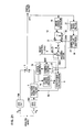
- FIG. 1 is a diagram illustrating a time interleave type ADC.
- FIG. 2 is a diagram illustrating an example of the frequency-divided sampling clocks ⁇ A and ⁇ B.
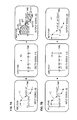
- FIGS. 3A to 3C are diagrams illustrating a skew error.
- FIG. 4 is a diagram illustrating an example of an ADC of the time interleave type.
- FIGS. 5A and 5B are diagrams for explaining the skew-error detecting circuit 10 .
- FIG. 6 is a circuit diagram of the adaptive filter 7 .
- FIGS. 7A and 7B are diagrams illustrating the operation of the adaptive filter.
- FIG. 8 is a diagram illustrating a waveform of the sinc function.
- FIG. 9 is a diagram illustrating the operation of the adaptive filter that uses filter coefficients by sinc functions.
- FIG. 10 is a diagram illustrating a waveform in an example in which the phase shift amount (delay amount) FD of the sinc function h(n) is a non-integer.
- FIG. 11 is a diagram illustrating a frequency characteristic of the transfer function.
- FIG. 12 is a diagram illustrating a characteristic of the differential value H′.
- FIG. 13 is a diagram illustrating a frequency characteristic of the group delay D( ⁇ ).
- FIG. 14 is a diagram illustrating specific waveform examples of the group delay characteristic D( ⁇ ) and the frequency characteristic H( ⁇ ).
- FIGS. 15A and 15B are diagrams illustrating a frequency characteristic of the group delay D( ⁇ ) and skew correction control of the adaptive filter in which the coefficient by the sinc function is set.
- FIGS. 16A and 16B are diagrams illustrating a problem of the skew correction control performed when an input signal has a high frequency.
- FIG. 17 is a diagram for explaining a first skew correction method in this embodiment.
- FIG. 18 is a diagram for explaining a second skew correction method in this embodiment.
- FIG. 19 is a configuration diagram of the time interleave ADC in the first embodiment.
- FIG. 20 is a flowchart for explaining the operation of the skew correction circuit 20 of the time interleave ADC illustrated in FIG. 19 .
- FIG. 21 is a configuration diagram of a time interleave ADC in a second embodiment.
- FIG. 22 is a flowchart for explaining the operation of the skew correction circuit 20 of the time interleave ADC illustrated in FIG. 21 .
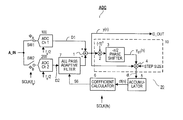
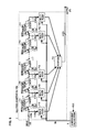
- FIG. 1 is a diagram illustrating a time interleave type ADC.
- the time interleave type ADC includes a plurality of (two in an example illustrated in FIG. 1 ) ADC channels 100 and 200 configured to convert an analog input signal A_IN into a digital output signal in a time interleave manner and a channel combiner 1 configured to combine channel digital signals D 1 and D 2 respectively output by the plurality of ADC channels 100 and 200 to generate a digital output signal D_OUT.
- the channel combiner 1 is, for example, an adder.
- the analog input signal A_IN is input to the ADC channels 100 and 200 respectively via switches SW 1 and SW 2 .
- the switches SW 1 and SW 2 repeat ON and OFF in a time interleave manner in synchronization with a sampling clock SCLK having a sampling frequency fs.
- the switches SW 1 and SW 2 are turned on in synchronization with rising edges (or falling edges) of sampling clocks ⁇ A and ⁇ B having a frequency fs/2 obtained by dividing the sampling clock SCLK having the sampling frequency fs by two (by N when the number of channels is N).
- the switches SW 1 and SW 2 respectively input the analog input signals A_IN to the ADC channels 100 and 200 corresponding thereto while the sampling clocks ⁇ A and ⁇ B are at an H level (or an L level).
- the ADC channels 100 and 200 respectively include ADC circuits and convert the analog input signal A_IN into digital signals D 1 and D 2 .
- the ADC circuits included in the ADC channels perform AD conversion at a period of a frequency fs/2 obtained by dividing the sampling clock SCLK of the sampling frequency fs by two, i.e., at a period 2/fs twice as long as the period of the sampling frequency fs. Therefore, the ADC circuits of the ADC channels only have to perform the AD conversion at a period twice as long as a sampling period.
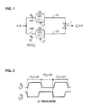
- FIG. 2 is a diagram illustrating an example of the frequency-divided sampling clocks ⁇ A and ⁇ B.
- an ON duty ratio of the sampling clock ⁇ A is 50%.
- timing of a rising edge of the sampling clock ⁇ B, a phase of which is inverted from a phase of the sampling clock ⁇ A is earlier than ideal timing 1/fs by ⁇ t/2.
- a skew error occurs in the AD-converted channel digital output signals D 1 and D 2 because of such deviation (skew) of the sampling timing of the ADCs.
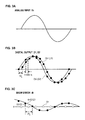
- FIGS. 3A to 3C are diagrams illustrating a skew error.
- An analog input signal fin is illustrated in FIG. 3A .
- the sampling timing of the period 1/fs and digital output signals D 1 , D 2 AD-converted by the ADC channels 100 and 200 are illustrated in FIG. 3B .
- the analog input signal A_IN is a sine wave or a cosine wave.
- FIG. 2 when a skew ⁇ t is present between sampling timings of both the channels, the other ADC channel is sampled at timing deviating from timing just in the middle of the sampling timing of one ADC channel.
- FIG. 3B when the digital output signals D 1 and D 2 of both the ADC channels are seen at the sampling timing of the period 1/fs, the digital output signals D 1 and D 2 have a phase difference corresponding to the skew ⁇ t.
- the digital output signal D 1 on the ADC channel 100 side has a phase later than a phase of the digital output signal D 2 on the ADC channel 200 side.
- a combined digital output signal D_OUT has a skew error dt illustrated in FIG. 3C with respect to the original analog input signal A_IN.
- the skew error dt is a difference D 2 ⁇ D 1 between the digital output signals D 1 and D 2 .
- the amplitude of the skew error dt is larger.
- the skew ⁇ t of the sampling clocks is zero, the phases of the digital output signals D 1 and D 2 illustrated in FIG. 3B coincide with each other.
- the skew error dt illustrated in FIG. 3C is zero at all the sampling timings.
- a difference between waveforms of the two digital outputs D 1 and D 2 is an error caused by the skew of the sampling clocks, i.e., a skew error.
- the difference is included in the digital output signal D_OUT obtained by combining the outputs of the two ADC channels.
- a skew error is zero as indicated by white circles on the abscissa in FIG. 3C .
- a value obtained by sampling and AD-converting the digital output D 2 has an error corresponding to the difference D 2 ⁇ D 1 of the digital outputs D 2 and D 1 as indicated by black circles in FIG. 3C .
- the combined digital output signal D_OUT includes an image signal component (a spurious component) due to the skew error, which is the difference between the digital outputs D 1 and D 2 at the sampling clock ⁇ B, in addition to an analog input signal component (a value of the digital output D 1 ).
- the skew error occurs at every period 2/fs of the sampling clock ⁇ B (frequency fs/2).
- the skew error has a value corresponding to a value of an envelope of a period 1/fin of the analog input signal (a waveform of D 1 ).
- a phase of the skew error shifts by ⁇ /2 from the phase of the analog input signal. Therefore, the image signal component due to the skew error is a waveform having a high frequency fs/2, which is a half of the sampling frequency fs and a low frequency of a frequency fin of the analog input signal (the waveform of D 1 ).
- a frequency of the image signal component is fs/2 ⁇ fin.
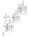
- FIG. 4 is a diagram illustrating an example of an ADC of the time interleave type.
- This example is an ADC that calibrates an image signal component, which is a skew error, on the background.
- This example is also an example including the two ADC channels 100 and 200 .
- the ADC of the time interleave type illustrated in FIG. 4 includes the two ADC channels 100 and 200 and the adder 1 configured to combine the digital outputs D 1 and D 2 of the ADC channels 100 and 200 . Further, the ADC includes an adaptive filter 7 for performing a phase shift for advancing or delaying the phase of the digital output D 2 of the ADC 200 of the second channel.
- the ADC illustrated in FIG. 4 includes a correction circuit 20 .
- the correction circuit 20 detects a skew error from the digital output signal D_OUT combined by the adder 1 , and generates a coefficient S 6 of the adaptive filter 7 so as to perform a phase shift according to the skew of the digital output D 2 , and suppress or eliminate the skew error of the combined digital output signal D_OUT.
- the correction circuit 20 includes a skew-error detecting circuit 10 configured to detect a skew error from the combined digital output signal D_OUT, an accumulator 5 configured to generate an average dt(n) of the skew error, and a coefficient calculator 6 configured to generate the coefficient S 6 of the adaptive filter 7 on the basis of the average dt(n) of the skew error.
- the correction circuit 20 calculates the average dt(n) (also referred to as skew error estimated amount) of the skew error as a value corresponding to the skew ⁇ t and sets, in the adaptive filter 7 , the coefficient S 6 for suppressing the average dt(n) of the skew error.
- the correction circuit 20 sets, in the adaptive filter 7 , the coefficient S 6 for performing a phase shift corresponding to the skew ⁇ t illustrated in FIG. 3B .
- the correction circuit 20 calculates the skew error estimated amount dt(n) from the digital output signal D_OUT using the skew-error detecting circuit 10 and the accumulator 5 and calculates the filter coefficient S 6 on the basis of the estimated amount using the coefficient calculator 6 .
- n represents the number of times of sampling.
- the adaptive filter 7 corrects the digital output D 2 of the second ADC channel 200 to a digital value of a phase-shifted signal according to the filter coefficient S 6 .
- the correction circuit 20 calculates the skew error estimated amount dt(n) again from the digital output signal D_OUT obtained as a result of the correction and calculates the filter coefficient S 6 .
- the correction circuit 20 repeats such processing until the skew error estimated amount dt(n) becomes asymptotic to near zero, whereby the skew error is corrected.
- FIGS. 5A and 5B are diagrams for explaining the skew-error detecting circuit 10 .
- an analog input signal component (frequency fin) and an image component (frequency fs/2 ⁇ fin) due to a skew error are illustrated with a normalized frequency plotted on the abscissa and power plotted on the ordinate.
- the skew-error detecting circuit 10 includes a frequency shift circuit 2 configured to multiply the combined digital output signal D_OUT (or y(n)) with a signal ( ⁇ 1) n , a sign of which is inverted to +1, ⁇ 1, +1, and ⁇ 1 at every sampling timing n.
- the signal ( ⁇ 1) n is a signal that changes at the period 2/fs twice as long as the sampling period 1/fs.
- a frequency of the signal ( ⁇ 1) n is fs/2.
- the frequency shift circuit 2 is a kind of mixer circuit including a multiplication circuit. Therefore, in an output yd 1 ( n ) of the frequency shift circuit 2 , as illustrated in FIG. 5B , an image component of the frequency fs/2 ⁇ fin is shifted to the frequency fin, which is a difference between the frequency fs/2 ⁇ fin and the frequency fs/2 of the signal ( ⁇ 1) n . An input signal of the frequency fin is shifted to the frequency fs/2 ⁇ fin, which is a difference between the frequency fin and the frequency fs/2 of the signal ( ⁇ 1) n .
- the skew-error detecting circuit 10 includes a phase shift circuit 3 configured to shift a phase of an output of the frequency shift circuit 2 by ⁇ /2.
- the input signal component and the image component of the combined digital output signal y(n) illustrated in FIG. 5A change to signals, phases of which are the same or inverted. The same applies to an image component and an input signal component of the output signal yd 1 ( n ) of the phase shift circuit 3 illustrated in FIG. 5B .
- a signal obtained by shifting the skew error dt by ⁇ /2 has a phase opposite to or the same as the phase of the input signal D 2 depending on whether a phase of an ADC channel Ch 2 side is delayed or advanced with respect to a Ch 1 side.
- the multiplier 4 in the skew-error detecting circuit 10 multiplies together the combined digital output signal y(n) and the output signal yd 1 ( n ) of the phase shift circuit 3 , and outputs a value obtained by adding up a multiplication value of the input signal component (fin) of the combined digital output signal y(n) and the image component (fin) of the output signal yd 1 ( n ) of the phase shift circuit 3 , and a multiplication value of the image component (fs/2 ⁇ fin) of the combined digital output signal y(n) and the input signal component (fs/2 ⁇ fin) of the output signal yd 1 ( n ) of the phase shift circuit 3 .
- the multiplier 4 outputs a value proportional to the amplitude of the image component. Moreover, the polarity of the skew error dt of the output of the multiplier 4 is opposite depending on whether a phase of the ADC channel Ch 2 side is delayed or advanced with respect to the Ch 1 side. Since frequencies of the multiplied signals coincide with each other, the output does not include a frequency component.
- the accumulator 5 in the correction circuit 20 integrates and averages the output of the multiplier 4 and removes an AC component of the output. Therefore, the average dt(n) of the skew error output by the accumulator 5 is an average updated at every sampling timing and is a value corresponding to the magnitude of the skew ⁇ t.
- the average dt(n) of the skew error indicates the direction of the skew as polarity.
- a coefficient calculating circuit 6 calculates, on the basis of the average dt(n) of the skew error corresponding to the magnitude of the skew, the coefficients S 6 for setting a phase shift amount of the adaptive filter 7 to suppress the skew error and sets the coefficient S 6 in the adaptive filter 7 .
- This feedback control is repeated in synchronization with the sampling clock (or a clock obtained by dividing the sampling clock), whereby the average dt(n) of the skew error is suppressed to be close to zero.
- a step size is given to the multiplier 4 as a coefficient.
- the step size is a coefficient for controlling the speed of the feedback control. When the step size is large, although the feedback control settles faster, overshoot and undershoot also increase. When the step size is small, although overshoot and undershoot decrease, the feedback control settles slowly.
- FIG. 6 is a circuit diagram of the adaptive filter 7 .
- the adaptive filter 7 outputs an output digital signal y(t) obtained by correcting an n-bit input digital signal x(t) to a desired waveform according to the coefficient S 6 .
- the adaptive filter 7 outputs the output digital signal y(t) obtained by shifting a phase of the input digital signal x(t) by a desired phase shift amount according to the coefficient S 6 .
- This phase shift amount of the adaptive filter 7 is a correction amount.
- the adaptive filter 7 includes a plurality of delay circuits 11 including, by the number of bits, delay flip-flops DFF for delaying the input digital signal x(t) by one clock. Further, the adaptive filter 7 includes a plurality of multipliers 712 including input nodes and output nodes of the delay circuits 711 as taps and configured to respectively multiply digital values of the taps and the coefficient S 6 output by the coefficient calculating circuit 6 and set in the taps, and an adder 713 configured to add up outputs of the multipliers 712 . A digital output of the adder 713 is an output digital signal y(t).
- the adaptive filter 7 illustrated in FIG. 6 is a higher-order filter as the number of taps is larger.
- FIGS. 7A and 7B are diagrams illustrating the operation of the adaptive filter.
- the input digital signal x(t), a delta function ⁇ (t) used as the coefficient S 6 , and the output digital signal y(t) are illustrated.
- the abscissa is a time axis.
- the abscissa represents tap positions in the adaptive filter illustrated in FIG. 6 .
- the adaptive filter 7 is an all-pass filter that allows all the input digital signal x(t) to pass. Therefore, the adaptive filter 7 executes a convolutional operation of the input digital signal x(t) and the Dirac delta function ⁇ (t) as indicated by the following Expression (1):
- T represents a constant and N represents the number of taps.
- the input digital signal x(t) is a digital value that changes at a sampling interval of time T.
- the adaptive filter 7 sequentially outputs, in synchronization with a sampling dock, input digital values of the center tap of the input digital signal x(t) delay-shifted at a sampling interval.
- the output digital signal y(t) sequentially have different digital values at every sampling period centering on respective sampling timings.
- the coefficient calculating circuit 6 shifts the delta function ⁇ (t) to the right side on the time axis (i.e., shifts the tap positions to the right side) to set the coefficient S 6 to, for example, a predetermined value other than zero at time 2T and zero at time other than the time 2T.
- the coefficient S 6 is set to such a coefficient
- the output digital signal y(t) at time nT output by the adaptive filter 7 in FIG. 7B has a digital value at time (n+2)T of the input digital signal x(t).
- the 7B is a signal obtained by shifting the phase of the input digital signal x(t) to the left by two taps, i.e., delaying the phase.
- the input digital signal x(t) shifts to the plurality of taps in the adaptive filter 7 as time elapses. Therefore, shifting the tap positions to the left means outputting a signal two docks in the past.
- the phase of the input digital signal is delayed. Conversely, when the delta function ⁇ (t) is shifted to the left side, it is possible to advance the phase.
- the phase of the delta function ⁇ (t) is shifted to set the coefficient in the adaptive filter 7 . Consequently, the adaptive filter 7 shifts the phase of the input digital signal in any direction and output the input digital signal.
- the correction circuit 20 and the adaptive filter 7 illustrated in FIG. 4 are explained above.
- the coefficient S 6 is a sinc function rather than the Dirac delta function.
- the coefficient calculating circuit 6 of the correction circuit 20 illustrated in FIG. 4 is realized with a coefficient by the sinc function rather than an ideal coefficient such as the Dirac delta function because of a circuit configuration.
- a filter coefficient by the sinc function points explained below is improved.
- FIG. 8 is a diagram illustrating a waveform of the sinc function.
- a sinc function h(n) is represented by the following Expression (2):
- FD represents a phase shift amount (or delay amount) in the abscissa direction corresponding to the plurality of taps of the adaptive filter 7 .
- FIG. 9 is a diagram illustrating the operation of the adaptive filter that uses filter coefficients by sinc functions.
- a filter function by a sinc function h 3 When a filter function by a sinc function h 3 is used, the input digital signal x(t) in a tap mT is output.
- a filter coefficient by a sinc function h 5 When a filter coefficient by a sinc function h 5 is used, the input digital signal x(t) in a tap (m+2) T is output and a phase is shifted (delayed).
- phase shift amount (delay amount) FD is an integer
- the phase shift amount (delay amount) FD needs to be set at accuracy of a non-integer (a number after the decimal point).
- FIG. 10 is a diagram illustrating a waveform in an example in which the phase shift amount (delay amount) FD of the sinc function h(n) is a non-integer.
- Expression (3) represents a transfer function Hd of the adaptive filter 7 in the case of the waveform in which, as illustrated in FIG. 8 , a coefficient of only one tap is 1 and coefficients of the other tamps are 0, i.e., an ideal transfer function Hd.
- the output digital signal y(t) obtained by shifting the phase of the input digital signal x(t) by FD is generated.
- a transfer function H of the adaptive filter that uses the coefficient of the sinc function is as represented by the following Expression (4).
- the sinc function h(n) is adopted, an error is added to the ideal transfer function Hd.
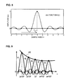
- FIG. 11 is a diagram illustrating a frequency characteristic of the transfer function.
- the error indicated by Expressions (5) and (6) is a negligible degree when the input digital signal x(t) has a low frequency.
- the transfer function H is the ideal value 1. However, when the input digital signal x(t) has a high frequency, the error increases.
- the transfer function H decreases in a high frequency band when the phase shift amount FD is positive and increases when the phase shift amount FD is negative (a broken line). “a” in FIG. 11 is an arbitrary value.
- the transfer function H of the adaptive filter 7 has the frequency characteristic illustrated in FIG. 11 .
- the filter coefficient by the sinc function illustrated in FIG. 10 has small amplitude and is positive and negative at values other than the peak value in the center. Therefore, when the analog input signal fin has a low frequency, the amplitude in the plurality of taps in the adaptive filter 7 gently changes.
- cumulative values of multiplication values of the taps other than the tap in the center are offset by a positive coefficient and a negative coefficient. A value close to the ideal value is output. This is the reason why the transfer function H is 1 in a low frequency domain in FIG. 11 .
- the analog input signal fin has a high frequency
- the amplitude of input signals in the plurality of taps in the adaptive filter substantially fluctuates.
- the offset effect by the positive and negative values of the filter coefficient is weakened and the error increases.
- the transfer function H falls or rises from the ideal value 1.
- the falling or rising of the transfer function H from the ideal value 1 means that an output signal of the adaptive filter 7 is not equal to an input signal and has an error.
- the offset effect is intensified and the frequency characteristic H is 1 up to a high frequency. Conversely, when the number of taps is small, the offset effect is weakened and the transfer function H falls or rises from 1 even at a low frequency.
- a group delay amount (a phase shift amount) of the adaptive filter is explained.
- the following Expression (7) represents a frequency response of the adaptive filter 7 .
- a frequency characteristic of the adaptive filter 7 has an amplitude characteristic G( ⁇ ) and a phase characteristic ⁇ ( ⁇ ).
- Expression (7) corresponds to the transfer function H of Expression (4).
- G( ⁇ ) represents an amplitude characteristic and ⁇ ( ⁇ ) represents a phase characteristic.
- a group delay characteristic (a phase shift amount) D( ⁇ ) of the adaptive filter 7 is obtained by differentiating the phase characteristic ⁇ ( ⁇ ) with respect to the angular frequency ⁇ from Expression (7).
- the group delay characteristic D( ⁇ ) is as represented by the following Expression (8):
- F D represents a delay amount of the filter.
- the group delay D( ⁇ ) has a characteristic corresponding to a differential value H′ of the transfer function H of Expression (7), i.e., Expression (4).
- the differential value H′ is obtained by differentiating the characteristic illustrated in FIG. 11 with respect to the angular frequency ⁇ .
- FIG. 12 is a diagram illustrating a characteristic of the differential value H′.
- the gradient of the graph of the transfer function H illustrated in FIG. 11 is H′. Therefore, the differential value H′ in FIG. 12 is 0 in a low frequency domain. In a high frequency domain, the differential value H′ is minus when the transfer function H falls and is plus when the transfer function H rises.
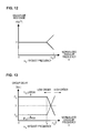
- FIG. 13 is a diagram illustrating a frequency characteristic of the group delay D( ⁇ ).
- the phase shift amount FD is added to H′. Therefore, when FD is positive, a characteristic chart illustrated in FIG. 13 is a characteristic indicated by a solid line shifted in the positive direction of the ordinate. When FD is negative, the characteristic chart is a characteristic indicated by a broken line shifted in the negative direction of the ordinate.
- the positive phase shift amount FD When an absolute value of the positive phase shift amount FD is increased, the characteristic shifts in the positive direction.
- an absolute value of the negative phase shift amount FD is increased, the characteristic shifts in the negative direction.
- a frequency f 4 at which the group delay falls or rises is higher as the adoptive filter 7 is a higher-order filter (having a larger number of taps) and is lower as the adaptive filter 7 is a lower-order filter (having a smaller number of taps).
- FIG. 14 is a diagram illustrating specific waveform examples of the group delay characteristic D( ⁇ ) and the frequency characteristic H( ⁇ ).
- the frequency characteristic H( ⁇ ) of the transfer function of the adaptive filter 7 slightly falls in a high-frequency domain. The fall is seen in an enlarged view of H( ⁇ ).
- the group delay characteristic D( ⁇ ) corresponding to a differential value of H( ⁇ ) falls to the minus side in the high-frequency domain.
- the specific waveform example in FIG. 14 coincides with the frequency characteristic of the group delay illustrated in FIG. 13 .
- the coefficient by the sinc function is set in the adaptive filter 7 and a phase is about to be shifted.
- a phase is about to be shifted.
- the input signal has a low frequency
- the input signal has a high frequency
- the direction of the phase shift is opposite to the direction corresponding to the delay amount FD.
- the gradient of the fall indicated by the solid line (or the rise indicated by the broken line) in a frequency domain higher than the frequency f 4 is steeper when the delay amount FD is increased.
- the group delay amount D( ⁇ ) has a peculiar frequency characteristic. Because of such a frequency characteristic, it is preferable to contrive the feedback control of the skew error suppression by the correction circuit 20 illustrated in FIG. 4 . This point is explained below.
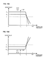
- FIGS. 15A and 15B are diagrams illustrating a frequency characteristic of the group delay D( ⁇ ) and skew correction control of the adaptive filter in which the coefficient by the sinc function is set. It is assumed that a frequency of an input signal to the adaptive filter is fin. The frequency fin is sufficiently low compared with the sampling frequency fs/2.
- a phase shift amount (a delay amount) necessary in the adaptive filter in order to suppress a skew included in the digital signal D 2 on the ADC channel 200 side is SK 1 .
- a phase shift amount of the sinc function also needs to be set to SK 1 . Therefore, in this case, the coefficient calculating circuit 6 illustrated in FIG. 4 calculates a coefficient while controlling the phase shift amount FD of the sinc function to ⁇ t 1 and ⁇ t 2 in a skew correction direction SCD 1 indicated by an arrow and sets the coefficient in the adaptive filter. Consequently, it is possible to suppress the average dt(n) of the skew error and then match the phase shift amount FD to the target phase shift amount SK 1 .
- a sign of a phase shift amount (a delay amount) SK 2 necessary for suppressing a skew included in the digital signal D 2 on the ADC channel 200 side is opposite to the sign of the phase shift amount SK 1 .
- the coefficient calculating circuit 6 illustrated in FIG. 4 calculates a coefficient while controlling the phase shift amount FD of the sinc function to ⁇ t 1 and ⁇ t 2 in a skew correction direction SCD 2 indicated by an arrow and sets the coefficient in the adaptive filter. Consequently, it is possible to suppress the average dt(n) of the skew error and then match the phase shift amount FD to the target phase shift amount SK 2 .
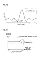
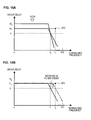
- FIGS. 16A and 16B are diagrams illustrating a problem of the skew correction control performed when an input signal has a high frequency.
- the frequency fin of the input signal is a high frequency closer to the sampling frequency fs/2 and is higher than a frequency f 1 at a zero-cross point where the group delay of the adaptive filter becomes polarity opposite to the set delay amount FD.
- a phase shift amount (a delay amount) necessary for skew correction is SK 3 .
- the coefficient calculating circuit 6 calculates a coefficient while controlling the phase shift amount FD of the sinc function to ⁇ t 1 and ⁇ t 2 in a skew correction direction SCD 3 and sets the coefficient in the adaptive filter as in FIG. 15A , since the frequency fin of the input signal is higher than the frequency f 1 at the zero-cross point, a delay amount of the adaptive filter changes in a direction of the opposite polarity. Therefore, it is impossible to set the delay amount of the adaptive filter to the delay amount SK 3 necessary for the skew correction irrespective of how much the phase shift amount FD is increased in the skew correction direction SCD 3 .
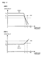
- FIG. 17 is a diagram for explaining a first skew correction method in this embodiment.
- a phase shift amount (a delay amount) necessary for skew correction is SK 4 .
- the frequency fin of the input signal is higher than the frequency f 1 at the zero-cross point, i.e., f 1 ⁇ fin ⁇ fs/2.
- the coefficient calculating circuit 6 calculates a coefficient for controlling the phase shift amount FD of the sinc function to ⁇ t 1 and ⁇ t 2 in a skew correction direction SCD 4 - 1 and sets the coefficient in the adaptive filter such that the phase shift amount (the delay amount) SK 4 is obtained.
- the skew error dt(t) increases to the contrary. This is because, as illustrated in FIG. 17 , as the frequency characteristic of the group delay, in a frequency domain higher than the frequency f 1 at the zero-cross point, the phase shift of the adaptive filter increases in the negative direction as the phase shift amount FD is increased in the positive direction.
- the phase shift amount FD is negative, the phase shift of the adaptive filter is in the positive direction at the frequency fin (>f 1 ).
- the absolute value of the phase shift amount FD is increased, the phase shift amount (the delay amount) increases in the positive direction.
- Step 2 in FIG. 17 it is possible to give the necessary phase shift SK 4 to the adaptive filter.
- the skew error dt(t) is suppressed.
- the phase shift amount (the delay amount) necessary for skew correction is SK 4 in the positive direction.
- the same control is possible when the phase shift amount is a negative phase shift amount.
- the coefficient calculating circuit 6 only has to perform control the coefficient to gradually increase the FD absolute value of the phase shift amount FD from a negative value and, when the absolute value reaches a maximum value, invert the polarity and gradually increase the absolute value of FD from a positive value.
- FIG. 18 is a diagram for explaining a second skew correction method in this embodiment.
- the frequency fin of the input signal is lower than the frequency f 1 at the zero-cross point and higher than a frequency f 2 at which the group delay starts to decrease (when the group delay has negative polarity, a frequency at which the group delay starts to increase), i.e., f 2 ⁇ fin ⁇ f 1 .
- f 2 ⁇ fin ⁇ f 1
- correction control in Step 1 and Step 2 is the same as the correction control in FIG. 17 .
- the coefficient calculating circuit 6 performs control the coefficient to gradually increase the FD absolute value of the phase shift amount FD from a positive value and, when the absolute value reaches a maximum value, in Step 2, inverts the polarity and gradually increases the absolute value of FD from a negative value.
- the frequency fin is in the relation f 2 ⁇ fin ⁇ f 1 , it is impossible to adjust the group delay with respect to the frequency fin of the adaptive filter to SK 5 .
- the coefficient calculating circuit 6 reduces the number of taps of the adaptive filter and reduces a filter order.
- a coefficient set in the multipliers 712 at both end sides of the adaptive filter only has to be set to zero to prevent outputs of the both sides multipliers 712 from being added to the adder 713 .
- the order of the filter decreases, in the frequency characteristic of the group delay, a frequency f 2 at which a group delay amount falls (or rises) is low. Therefore, the order of the filter is reduced until the frequency fin of the input signal becomes higher than the frequency f 1 at the zero-cross point.
- Step 2 the absolute value of the phase shift amount FD is gradually increased from a negative value.
- the group delay amount increases in the positive direction at the frequency fin of the input signal. It is possible to give a necessary group delay amount of the delay amount SK 5 to the frequency fin.
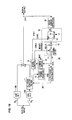
- FIG. 19 is a configuration diagram of the time interleave ADC in the first embodiment.
- a polarity inverting circuit 12 that inverts the polarity of the skew error dt is provided between the skew-error detecting circuit 10 and the accumulator 5 and a comparator 17 that determines whether the average dt(n) of the skew error reaches a maximum allowable value MAX, a state control circuit 18 that controls Steps 1, 2, and 3 explained in FIGS. 16A and 16B and FIG. 17 , and a filter-order deciding circuit 19 that determines the order of the adaptive filter 7 are provided.
- the polarity inverting circuit 12 includes a multiplier 14 configured to multiply the skew error dt with ( ⁇ 1) to invert polarity and a multiplexer 13 configured to select, on the basis of a control signal S 18 - 1 , whether an output of the skew-error detecting circuit 10 is output without inverting the polarity or after inverting the polarity.
- the accumulator 5 includes a delay FF circuit 15 configured to delay an output of the polarity inverting circuit 12 by one clock and an adder 16 configured to add an output of the delay circuit 15 to the present skew error dt, which is the output of the polarity inverting circuit 12 .
- an output of the accumulator 5 is the average dt(n) of a skew error obtained by accumulating the skew error dt reduced at a predetermined ratio according to the step size in the skew-error detecting circuit 10 .
- the state control circuit 18 controls, with a case control signal S 18 - 1 , presence or absence of the polarity inversion by the polarity inverting circuit 12 and resets, with a reset control signal S 18 - 2 , an accumulation value of the accumulator 5 .
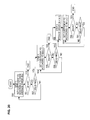
- FIG. 20 is a flowchart for explaining the operation of the skew correction circuit 20 of the time interleave ADC illustrated in FIG. 19 .
- the skew correction circuit 20 performs the three steps in FIG. 18 in order as skew correction.
- the operation of the skew correction circuit 20 illustrated in FIG. 19 is explained below according to the flowchart of FIG. 20 .
- the state control circuit 18 sets the case control signal S 18 - 1 to 0 to control the polarity inverting circuit 12 to non-inverting and sets the reset control signal S 18 - 2 to a reset state to reset the delay FF circuit 15 in the accumulator 5 for resetting the accumulation value.
- the coefficient calculating circuit 6 calculates the necessary phase shift amount (delay amount) FD, calculates the coefficient S 6 using the sinc function, and sets the coefficient S 6 in the multipliers 12 (see FIG. 6 ) of the taps of the adaptive filter 7 (S 50 ).
- the skew correction control ends (YES in S 51 ).
- the state control circuit 18 repeats Step S 50 while an absolute value of the average dt(n) does not reach the allowable maximum value MAX (NO in S 52 ) or the phase shift amount FD corresponding to the coefficient S 6 does not reach the maximum amount. Consequently, the average dt(n) of the skew error is asymptotic to zero.
- the comparator 17 determines whether the absolute value of the average dt(n) of the skew error reaches the maximum value MAX.
- the comparator 17 informs the state control circuit 18 of a result of the determination.
- the coefficient calculation circuit 6 determines whether FD corresponding to S 6 reaches to the maximum, and informs to the state control circuit 18 of the determination.
- the skew correction control in Step 1 is as explained with reference to FIGS. 17 and 18 .
- the coefficient calculating circuit 6 determines the polarity of the necessary phase shift amount (delay amount) FD according to the polarity of the average dt(n) of the skew error.
- the coefficient calculating circuit 6 determines the magnitude of the necessary phase shift amount (delay amount) FD according to the magnitude of the average dt(n) of the skew error.
- the phase shift amount (the delay amount) FD corresponds to the group delay amount on the ordinate in FIGS. 17 and 18 .
- the state control circuit 18 sets the case control signal S 18 - 1 to 1, sets the reset control signal S 18 - 2 to the reset state, and shifts to the control in Step 2. Consequently, the polarity of the skew error dt output by the skew-error detecting circuit 10 is inverted and the accumulation value is reset.
- the coefficient calculating circuit 6 calculates the necessary phase shift amount (delay amount) FD, calculates the coefficient S 6 using the sinc function, and sets the coefficient S 6 in the multipliers 12 of the taps of the adaptive filter 7 (S 54 ). Step S 54 is repeated while the average dt(n) of the skew error does not decrease to zero (NO in S 55 ) and the absolute value of the average dt(n) does not reach the maximum MAX or FD does not reach the maximum (No in S 56 ).
- Step 2 according to the polarity inversion of the polarity inverting circuit 12 , the coefficient calculating circuit 6 sets the coefficient S 6 according to an imaginary phase shift amount ⁇ SK 4 obtained by inverting the polarity of the phase shift amount SK 4 necessary for the adaptive filter 7 . Therefore, the correction circuit 20 performs correction control to gradually increase the absolute value of the phase shift amount FD on the negative side and suppress the average dt(n) of the skew error.
- Step 2 the coefficient S 6 corresponding to the phase shift amount SK 4 necessary for the adaptive filter is set, the average of the skew error is appropriately controlled, and the skew correction control ends.
- the average dt(n) of the skew error is not appropriately controlled and reaches the maximum value MAX or FD reaches to the maximum (YES in S 56 ).
- the state control circuit 18 sets the reset control signal S 18 - 2 to the reset state, keeps the case control signal S 18 - 1 at 1, and controls the filter-order deciding circuit 19 to reduce the filter order (S 58 ). Consequently, the skew correction shifts to Step 3.
- the coefficient calculating circuit 6 sets the coefficient to the multipliers 12 at both the ends of the adaptive filter 7 to zero.
- Step 2 according to the magnitude and the polarity of the average value dt(n) of the skew error, the coefficient calculating circuit 6 calculates the necessary phase shift amount (delay amount) FD, calculates the coefficient S 6 using the sinc function, and sets the coefficient S 6 in the multipliers 12 of the taps of the adaptive filter 7 (S 59 ).
- Step S 59 is repeated while the average dt(n) of the skew error does not decrease to zero (NO in S 60 ) and the absolute value of the average dt(n) does not reach the maximum MAX or FD does not reach to the maximum (No in S 61 ).
- the state control circuit 18 sets the reset control signal S 18 - 2 to the reset state again, performs control for reducing the order of the adaptive filter 7 (S 58 ), and repeats the control in Step 2 in the same manner. Then, when the average dt(n) of the skew error is appropriately suppressed, the state control circuit 18 ends the skew correction.
- the skew correction circuit 20 appropriately sets the coefficient of the adaptive filter 7 , controls the order to an appropriate level, and performs the skew correction.
- FIG. 21 is a configuration diagram of a time interleave ADC in a second embodiment.
- the time interleave ADC additionally includes a case-control-signal generating circuit 30 including a band-pass filter 21 and an amplitude determining circuit 22 and configured to supply a case control signal to the multiplexer 13 of the polarity inverting circuit 12 and an AND gate 23 configured to input the average dt(n) of the skew error to the comparator 17 when the case control signal is 1.
- the case-control-signal generating circuit 30 determine, on the basis of a frequency of the combined digital output signal y(n), whether skew correction control of a case 1 is performed or the polarity of the skew error dt is inverted and skew correction control in cases 2 and 3 is performed. In other words, the case-control-signal generating circuit 30 determines whether the frequency fin of the input signal included in the combined digital output signal y(n) is in the relation of f 2 ⁇ fin in FIGS. 17 and 18 .
- the band-pass filter 21 is a low-pass filter that allows a frequency lower than the frequency f 2 to pass, therefore, fin ⁇ f 2 is determined when the amplitude of an output of the filter 21 is larger than a reference value, and the case control signal is set to 0 so that the polarity inverting circuit 12 does not invert the polarity. In this case, only Step 1 of the skew correction control is executed. On the other hand, when the amplitude of the output of the filter 21 is smaller than the reference value, it is determined that f 2 ⁇ fin, and the polarity inverting circuit 12 inverts the polarity. In this case, Steps 2 and 3 of the skew correction control are executed. The comparator 17 determines switching from Step 2 to Step 3. Therefore, the AND gate 23 inputs the average dt(n) of the skew error to the comparator 17 only when the case control signal is 1.
- the case-control-signal generating circuit 30 may receive an output of the ADC channel 100 or 200 .
- FIG. 22 is a flowchart for explaining the operation of the skew correction circuit 20 of the time interleave ADC illustrated in FIG. 21 .
- the skew correction circuit 20 performs control in Step 1 (S 50 to S 52 ) or performs control Steps 2 and 3 (S 54 to S 61 ) according to a case control signal of the case-control-signal generating circuit 30 (S 62 ). Therefore, unlike the operation flowchart of FIG. 20 in the first embodiment, the skew correction circuit 20 does not perform Steps 1, 2, and 3 in order but performs Step 1 or performs Steps 2 and 3. Therefore, it is possible to set the skew correction process shorter than the skew correction process in the first embodiment.
- the skew correction control in Steps 1, 2, and 3 is the same as the skew correction control in the first embodiment.
Landscapes
- Engineering & Computer Science (AREA)
- Theoretical Computer Science (AREA)
- Analogue/Digital Conversion (AREA)
Abstract
Description
- This application is based upon and claims the benefit of priority of the prior Japanese Patent Application No. 2012-55489, filed on Mar. 13, 2012, the entire contents of which are incorporated herein by reference.
- The present embodiments relate to an ADC and a correction circuit and a correction method for the ADC.
- An analog digital converter (ADC) is a circuit that converts an analog input signal into a digital output signal. In order to increase a sampling frequency of analog digital conversion, a time interleave ADC is proposed in which a plurality of ADCs (ADC channels) are provided and the plurality of ADCs convert an analog input signal into a digital output signal in order in a time division manner. The time interleave ADC is described in Japanese Patent Application Laid-Open No. 2005-348156 and Japanese Patent Application Laid-Open No. 2008-11189.
- The time interleave ADC enables a high-speed operation. However, when characteristics of the ADCs are different or a relation among timings when the ADCs operate deviates, an S/N ratio sometimes falls. As a method of correcting an error among the ADC channels, foreground calibration and background calibration are proposed. The former requires time for correction other than normal operation time of the ADCs. On the other hand, since the latter performs correction during a normal operation of the ADCs, it corrects, in background, an error caused by aged deterioration, a temperature change, or the like. A background calibration circuit is described in S. M. Jamal, et al., “A 10
b 120 Msample/s Time-Interleaved Analog-to-Digital Converter With Digital Background Calibration”, JSSC 2002. - In the background calibration circuit, an adaptive filter is provided in at least one of a plurality of ADC channels that operate in a time interleave (time division) manner. A coefficient of the adaptive filter is calculated on the basis of an added-up output obtained by adding up outputs of the plurality of ADC channels. The coefficient of the adaptive filter is controlled to suppress a spurious signal component of the added-up output. Consequently, a spurious signal component (an error signal component or an image signal component), which is an error (a skew error) caused by deviation (skew) of sampling timing of the time interleave, is suppressed.
- However, when a sinc function is used instead of a delta function as the coefficient of the adaptive filter, a desired phase shift control is possible as long as phase shift control is performed at accuracy of a tap of the adaptive filter. However, a characteristic of the adaptive filter has frequency dependency when the phase shift control is performed at accuracy smaller than the accuracy of the tap. Therefore, when an analog input signal has a high frequency, the desired phase shift control is difficult or impossible because of the frequency dependency.
- One aspect of an embodiment is an analog digital converter (hereinafter ADC) that samples an analog input signal at a sampling frequency and converts the analog input signal into a digital output signal,
- the ADC including:
- a plurality of ADC channels configured to convert the analog input signal into the digital output signal in a time interleave manner;
- a channel combiner configured to combine channel digital signals respectively output by the plurality of ADC channels and generate the digital output signal;
- an adaptive filter provided between an output of at least one of the plurality of ADC channels and the channel combiner; and
- a correction circuit configured to detect a skew error included in the digital output signal, generate a coefficient of the adaptive filter according to the skew error, and set the coefficient in the adaptive filter, wherein
- in a first setting, the correction circuit sets, according to the skew error, the coefficient such that the adaptive filter phase-shifts to one direction for advancing or delaying a phase of the channel digital signal and, in a second setting, the correction circuit sets, according to the skew error, the coefficient such that the adaptive filter phase-shifts to an opposite direction to the one direction and sets, in the adaptive filter, a coefficient with which the skew error is suppressed to a desired level.
- The object and advantages of the invention will be realized and attained by means of the elements and combinations particularly pointed out in the claims.
- It is to be understood that both the foregoing general description and the following detailed description are exemplary and explanatory and are not restrictive of the invention.
-
FIG. 1 is a diagram illustrating a time interleave type ADC. -
FIG. 2 is a diagram illustrating an example of the frequency-divided sampling clocks ΦA and ΦB. -
FIGS. 3A to 3C are diagrams illustrating a skew error. -
FIG. 4 is a diagram illustrating an example of an ADC of the time interleave type. -
FIGS. 5A and 5B are diagrams for explaining the skew-error detecting circuit 10. -
FIG. 6 is a circuit diagram of theadaptive filter 7. -
FIGS. 7A and 7B are diagrams illustrating the operation of the adaptive filter. -
FIG. 8 is a diagram illustrating a waveform of the sinc function. -
FIG. 9 is a diagram illustrating the operation of the adaptive filter that uses filter coefficients by sinc functions. -
FIG. 10 is a diagram illustrating a waveform in an example in which the phase shift amount (delay amount) FD of the sinc function h(n) is a non-integer. -
FIG. 11 is a diagram illustrating a frequency characteristic of the transfer function. -
FIG. 12 is a diagram illustrating a characteristic of the differential value H′. -
FIG. 13 is a diagram illustrating a frequency characteristic of the group delay D(ω). -
FIG. 14 is a diagram illustrating specific waveform examples of the group delay characteristic D(ω) and the frequency characteristic H(ω). -
FIGS. 15A and 15B are diagrams illustrating a frequency characteristic of the group delay D(ω) and skew correction control of the adaptive filter in which the coefficient by the sinc function is set. -
FIGS. 16A and 16B are diagrams illustrating a problem of the skew correction control performed when an input signal has a high frequency. -
FIG. 17 is a diagram for explaining a first skew correction method in this embodiment. -
FIG. 18 is a diagram for explaining a second skew correction method in this embodiment. -
FIG. 19 is a configuration diagram of the time interleave ADC in the first embodiment. -
FIG. 20 is a flowchart for explaining the operation of theskew correction circuit 20 of the time interleave ADC illustrated inFIG. 19 . -
FIG. 21 is a configuration diagram of a time interleave ADC in a second embodiment. -
FIG. 22 is a flowchart for explaining the operation of theskew correction circuit 20 of the time interleave ADC illustrated inFIG. 21 . -
FIG. 1 is a diagram illustrating a time interleave type ADC. The time interleave type ADC includes a plurality of (two in an example illustrated inFIG. 1 )ADC channels ADC channels channel combiner 1 is, for example, an adder. - The analog input signal A_IN is input to the
ADC channels FIG. 1 , since the ADC includes the two ADC channels, the switches SW1 and SW2 are turned on in synchronization with rising edges (or falling edges) of sampling clocks ΦA and ΦB having a frequency fs/2 obtained by dividing the sampling clock SCLK having the sampling frequency fs by two (by N when the number of channels is N). The switches SW1 and SW2 respectively input the analog input signals A_IN to theADC channels - The
ADC channels period 2/fs twice as long as the period of the sampling frequency fs. Therefore, the ADC circuits of the ADC channels only have to perform the AD conversion at a period twice as long as a sampling period. -
FIG. 2 is a diagram illustrating an example of the frequency-divided sampling clocks ΦA and ΦB. Ideally, an ON duty ratio of the sampling clock ΦA is 50%. However, as illustrated inFIG. 2 , when a period of the H level is 1/fs+Δt/2 and a period of the L level is 1/fs−Δt/2, timing of a rising edge of the sampling clock ΦB, a phase of which is inverted from a phase of the sampling clock ΦA, is earlier thanideal timing 1/fs by −Δt/2. A skew error occurs in the AD-converted channel digital output signals D1 and D2 because of such deviation (skew) of the sampling timing of the ADCs. -
FIGS. 3A to 3C are diagrams illustrating a skew error. An analog input signal fin is illustrated inFIG. 3A . The sampling timing of theperiod 1/fs and digital output signals D1, D2 AD-converted by theADC channels FIG. 3B . As an example, the analog input signal A_IN is a sine wave or a cosine wave. As illustrated inFIG. 2 , when a skew Δt is present between sampling timings of both the channels, the other ADC channel is sampled at timing deviating from timing just in the middle of the sampling timing of one ADC channel. As a result, as illustrated inFIG. 3B , when the digital output signals D1 and D2 of both the ADC channels are seen at the sampling timing of theperiod 1/fs, the digital output signals D1 and D2 have a phase difference corresponding to the skew Δt. - In an example illustrated in
FIG. 3B , the digital output signal D1 on theADC channel 100 side has a phase later than a phase of the digital output signal D2 on theADC channel 200 side. - As a result, when the digital output signals D1 and D2 are combined by the
combiner 1, a combined digital output signal D_OUT has a skew error dt illustrated inFIG. 3C with respect to the original analog input signal A_IN. The skew error dt is a difference D2−D1 between the digital output signals D1 and D2. As the skew Δt is larger, the amplitude of the skew error dt is larger. When the skew Δt of the sampling clocks is zero, the phases of the digital output signals D1 and D2 illustrated inFIG. 3B coincide with each other. The skew error dt illustrated inFIG. 3C is zero at all the sampling timings. - As explained above, a difference between waveforms of the two digital outputs D1 and D2 is an error caused by the skew of the sampling clocks, i.e., a skew error. The difference is included in the digital output signal D_OUT obtained by combining the outputs of the two ADC channels. In a value obtained by sampling and AD-converting the digital output D1, a skew error is zero as indicated by white circles on the abscissa in
FIG. 3C . However, a value obtained by sampling and AD-converting the digital output D2 has an error corresponding to the difference D2−D1 of the digital outputs D2 and D1 as indicated by black circles inFIG. 3C . In other words, the combined digital output signal D_OUT includes an image signal component (a spurious component) due to the skew error, which is the difference between the digital outputs D1 and D2 at the sampling clock ΦB, in addition to an analog input signal component (a value of the digital output D1). - As illustrated in
FIG. 3C , the skew error occurs at everyperiod 2/fs of the sampling clock ΦB (frequency fs/2). The skew error has a value corresponding to a value of an envelope of aperiod 1/fin of the analog input signal (a waveform of D1). A phase of the skew error shifts by π/2 from the phase of the analog input signal. Therefore, the image signal component due to the skew error is a waveform having a high frequency fs/2, which is a half of the sampling frequency fs and a low frequency of a frequency fin of the analog input signal (the waveform of D1). A frequency of the image signal component is fs/2−fin. -
FIG. 4 is a diagram illustrating an example of an ADC of the time interleave type. This example is an ADC that calibrates an image signal component, which is a skew error, on the background. This example is also an example including the twoADC channels - Like the ADC illustrated in
FIG. 1 , the ADC of the time interleave type illustrated inFIG. 4 includes the twoADC channels adder 1 configured to combine the digital outputs D1 and D2 of theADC channels adaptive filter 7 for performing a phase shift for advancing or delaying the phase of the digital output D2 of theADC 200 of the second channel. The ADC illustrated inFIG. 4 includes acorrection circuit 20. Thecorrection circuit 20 detects a skew error from the digital output signal D_OUT combined by theadder 1, and generates a coefficient S6 of theadaptive filter 7 so as to perform a phase shift according to the skew of the digital output D2, and suppress or eliminate the skew error of the combined digital output signal D_OUT. Thecorrection circuit 20 includes a skew-error detecting circuit 10 configured to detect a skew error from the combined digital output signal D_OUT, anaccumulator 5 configured to generate an average dt(n) of the skew error, and acoefficient calculator 6 configured to generate the coefficient S6 of theadaptive filter 7 on the basis of the average dt(n) of the skew error. - Specifically, as illustrated in
FIGS. 3A to 3C , the skew error dt occurs at theperiod 2/fs twice as long as thesampling period 1/fs and fluctuates at an amplitude proportional to the magnitude of the skew Δt. Therefore, thecorrection circuit 20 calculates the average dt(n) (also referred to as skew error estimated amount) of the skew error as a value corresponding to the skew Δt and sets, in theadaptive filter 7, the coefficient S6 for suppressing the average dt(n) of the skew error. In other words, thecorrection circuit 20 sets, in theadaptive filter 7, the coefficient S6 for performing a phase shift corresponding to the skew Δt illustrated inFIG. 3B . - More specifically, the
correction circuit 20 calculates the skew error estimated amount dt(n) from the digital output signal D_OUT using the skew-error detecting circuit 10 and theaccumulator 5 and calculates the filter coefficient S6 on the basis of the estimated amount using thecoefficient calculator 6. In the skew error estimated amount dt(n), n represents the number of times of sampling. Theadaptive filter 7 corrects the digital output D2 of thesecond ADC channel 200 to a digital value of a phase-shifted signal according to the filter coefficient S6. Thecorrection circuit 20 calculates the skew error estimated amount dt(n) again from the digital output signal D_OUT obtained as a result of the correction and calculates the filter coefficient S6. Thecorrection circuit 20 repeats such processing until the skew error estimated amount dt(n) becomes asymptotic to near zero, whereby the skew error is corrected. -
FIGS. 5A and 5B are diagrams for explaining the skew-error detecting circuit 10. InFIG. 5A , an analog input signal component (frequency fin) and an image component (frequency fs/2−fin) due to a skew error are illustrated with a normalized frequency plotted on the abscissa and power plotted on the ordinate. - The skew-
error detecting circuit 10 includes afrequency shift circuit 2 configured to multiply the combined digital output signal D_OUT (or y(n)) with a signal (−1)n, a sign of which is inverted to +1, −1, +1, and −1 at every sampling timing n. The signal (−1)n is a signal that changes at theperiod 2/fs twice as long as thesampling period 1/fs. A frequency of the signal (−1)n is fs/2. - Therefore, the
frequency shift circuit 2 is a kind of mixer circuit including a multiplication circuit. Therefore, in an output yd1(n) of thefrequency shift circuit 2, as illustrated inFIG. 5B , an image component of the frequency fs/2−fin is shifted to the frequency fin, which is a difference between the frequency fs/2−fin and the frequency fs/2 of the signal (−1)n. An input signal of the frequency fin is shifted to the frequency fs/2−fin, which is a difference between the frequency fin and the frequency fs/2 of the signal (−1)n. - Further, as illustrated in
FIG. 3C , phases of the input signal fin and a signal of the image component (a skew error signal) deviate by π/2. Therefore, the skew-error detecting circuit 10 includes aphase shift circuit 3 configured to shift a phase of an output of thefrequency shift circuit 2 by −π/2. According to the −π/2 shift by thephase shift circuit 3, the input signal component and the image component of the combined digital output signal y(n) illustrated inFIG. 5A change to signals, phases of which are the same or inverted. The same applies to an image component and an input signal component of the output signal yd1(n) of thephase shift circuit 3 illustrated inFIG. 5B . - In short, as explained with reference to
FIGS. 3B and 3C , a signal obtained by shifting the skew error dt by −π/2 has a phase opposite to or the same as the phase of the input signal D2 depending on whether a phase of an ADC channel Ch2 side is delayed or advanced with respect to a Ch1 side. - Therefore, the
multiplier 4 in the skew-error detecting circuit 10 multiplies together the combined digital output signal y(n) and the output signal yd1(n) of thephase shift circuit 3, and outputs a value obtained by adding up a multiplication value of the input signal component (fin) of the combined digital output signal y(n) and the image component (fin) of the output signal yd1(n) of thephase shift circuit 3, and a multiplication value of the image component (fs/2−fin) of the combined digital output signal y(n) and the input signal component (fs/2−fin) of the output signal yd1(n) of thephase shift circuit 3. As a result, themultiplier 4 outputs a value proportional to the amplitude of the image component. Moreover, the polarity of the skew error dt of the output of themultiplier 4 is opposite depending on whether a phase of the ADC channel Ch2 side is delayed or advanced with respect to the Ch1 side. Since frequencies of the multiplied signals coincide with each other, the output does not include a frequency component. - Although the output dt of the
multiplier 4 has a value corresponding to the skew error, the skew error fluctuates as illustrated inFIG. 3C . Therefore, theaccumulator 5 in thecorrection circuit 20 integrates and averages the output of themultiplier 4 and removes an AC component of the output. Therefore, the average dt(n) of the skew error output by theaccumulator 5 is an average updated at every sampling timing and is a value corresponding to the magnitude of the skew Δt. The average dt(n) of the skew error indicates the direction of the skew as polarity. - Finally, in synchronization with the sampling clock SCLK(fs), a
coefficient calculating circuit 6 calculates, on the basis of the average dt(n) of the skew error corresponding to the magnitude of the skew, the coefficients S6 for setting a phase shift amount of theadaptive filter 7 to suppress the skew error and sets the coefficient S6 in theadaptive filter 7. This feedback control is repeated in synchronization with the sampling clock (or a clock obtained by dividing the sampling clock), whereby the average dt(n) of the skew error is suppressed to be close to zero. - A step size is given to the
multiplier 4 as a coefficient. The step size is a coefficient for controlling the speed of the feedback control. When the step size is large, although the feedback control settles faster, overshoot and undershoot also increase. When the step size is small, although overshoot and undershoot decrease, the feedback control settles slowly. -
FIG. 6 is a circuit diagram of theadaptive filter 7. Theadaptive filter 7 outputs an output digital signal y(t) obtained by correcting an n-bit input digital signal x(t) to a desired waveform according to the coefficient S6. In this embodiment, theadaptive filter 7 outputs the output digital signal y(t) obtained by shifting a phase of the input digital signal x(t) by a desired phase shift amount according to the coefficient S6. This phase shift amount of theadaptive filter 7 is a correction amount. - The
adaptive filter 7 includes a plurality ofdelay circuits 11 including, by the number of bits, delay flip-flops DFF for delaying the input digital signal x(t) by one clock. Further, theadaptive filter 7 includes a plurality ofmultipliers 712 including input nodes and output nodes of thedelay circuits 711 as taps and configured to respectively multiply digital values of the taps and the coefficient S6 output by thecoefficient calculating circuit 6 and set in the taps, and anadder 713 configured to add up outputs of themultipliers 712. A digital output of theadder 713 is an output digital signal y(t). Theadaptive filter 7 illustrated inFIG. 6 is a higher-order filter as the number of taps is larger. -
FIGS. 7A and 7B are diagrams illustrating the operation of the adaptive filter. InFIGS. 7A and 7B , the input digital signal x(t), a delta function δ(t) used as the coefficient S6, and the output digital signal y(t) are illustrated. The abscissa is a time axis. The abscissa represents tap positions in the adaptive filter illustrated inFIG. 6 . - The
adaptive filter 7 is an all-pass filter that allows all the input digital signal x(t) to pass. Therefore, theadaptive filter 7 executes a convolutional operation of the input digital signal x(t) and the Dirac delta function δ(t) as indicated by the following Expression (1): -
- where, T represents a constant and N represents the number of taps.
- As indicated by
FIG. 7A and Expression (1), the input digital signal x(t) is a digital value that changes at a sampling interval of time T. The delta function δ(t) has predetermined magnitude at time t=0 (in the center tap) and hasmagnitude 0 in the other times. Therefore, the plurality ofmultipliers 12 of theadaptive filter 7 multiply the input digital signal x(t) of the center tap (t=0) with a value of the delta function δ(t) at time t=0, multiply the input digital signal x(t) of the other taps (other than t=0) with avalue 0 other than time t=0, and output an added-up value of multiplication values obtained by the multiplication. Theadaptive filter 7 sequentially outputs, in synchronization with a sampling dock, input digital values of the center tap of the input digital signal x(t) delay-shifted at a sampling interval. In other words, as illustrated inFIG. 7A , the output digital signal y(t) sequentially have different digital values at every sampling period centering on respective sampling timings. - The phase shift by the coefficient S6 is explained. As illustrated in
FIG. 7B , thecoefficient calculating circuit 6 shifts the delta function δ(t) to the right side on the time axis (i.e., shifts the tap positions to the right side) to set the coefficient S6 to, for example, a predetermined value other than zero attime 2T and zero at time other than thetime 2T. When the coefficient S6 is set to such a coefficient, the output digital signal y(t) at time nT output by theadaptive filter 7 inFIG. 7B has a digital value at time (n+2)T of the input digital signal x(t). In other words, the output digital signal y(t) inFIG. 7B is a signal obtained by shifting the phase of the input digital signal x(t) to the left by two taps, i.e., delaying the phase. The input digital signal x(t) shifts to the plurality of taps in theadaptive filter 7 as time elapses. Therefore, shifting the tap positions to the left means outputting a signal two docks in the past. The phase of the input digital signal is delayed. Conversely, when the delta function δ(t) is shifted to the left side, it is possible to advance the phase. - As explained above, the phase of the delta function δ(t) is shifted to set the coefficient in the
adaptive filter 7. Consequently, theadaptive filter 7 shifts the phase of the input digital signal in any direction and output the input digital signal. Thecorrection circuit 20 and theadaptive filter 7 illustrated inFIG. 4 are explained above. - Points to be Improved of the Adaptive Filter
- In the following explanation, the coefficient S6 is a sinc function rather than the Dirac delta function. The
coefficient calculating circuit 6 of thecorrection circuit 20 illustrated inFIG. 4 is realized with a coefficient by the sinc function rather than an ideal coefficient such as the Dirac delta function because of a circuit configuration. However, when a filter coefficient by the sinc function is used, points explained below is improved. -
FIG. 8 is a diagram illustrating a waveform of the sinc function. A sinc function h(n) is represented by the following Expression (2): -
- where, FD represents a phase shift amount (or delay amount) in the abscissa direction corresponding to the plurality of taps of the
adaptive filter 7. As it is evident fromFIG. 8 , when a value n of the abscissa is equal to the phase shift amount FD (FD=3 inFIG. 8 ) (n=FD=3), an output of the sinc function h(n) is 1. When the value n of the abscissa is other than the phase shift amount FD (FD=3), the output of the sinc function h(n) is 0. When theadaptive filter 7 uses the filter coefficient by the above sinc function h(n), theadaptive filter 7 is an all-pass filter like the filter that uses the filter coefficient by the delta function δ(t). -
FIG. 9 is a diagram illustrating the operation of the adaptive filter that uses filter coefficients by sinc functions. When a filter function by a sinc function h3 is used, the input digital signal x(t) in a tap mT is output. When a filter coefficient by a sinc function h5 is used, the input digital signal x(t) in a tap (m+2) T is output and a phase is shifted (delayed). - Even when the coefficients by the sinc functions are set as explained above, when the phase shift amount (delay amount) FD is an integer, it is possible to perform phase shift control same as the phase shift control performed by using the coefficient by the delta function. However, a skew amount between the ADC channels in the time interleave ADC is time shorter than a period of a sampling clock. Therefore, the phase shift amount (delay amount) FD needs to be set at accuracy of a non-integer (a number after the decimal point).
-
FIG. 10 is a diagram illustrating a waveform in an example in which the phase shift amount (delay amount) FD of the sinc function h(n) is a non-integer. In this example, the phase shift amount FD is 3.2, which is a non-integer. Therefore, although a coefficient input to the multipliers of the taps in theadaptive filter 7 takes a large value close to 1 at n=3, the coefficient is not zero at n=−2 to 2 and 4 to 8. However, the phase shift amount FD is controlled to n=3.2 according to a large value at n=3 and a relatively large value at n=4. The corresponding multipliers in theadaptive filter 7 output relatively small multiplication values according to relatively small values at the values other than n=3 and 4. Therefore, when the phase-shift amount FD is a non-integer, the output digital signal y(t) of theadaptive filter 7 is a value different from the input digital signal x(t). - The following Expression (3) represents a transfer function Hd of the
adaptive filter 7 in the case of the waveform in which, as illustrated inFIG. 8 , a coefficient of only one tap is 1 and coefficients of the other tamps are 0, i.e., an ideal transfer function Hd. -
[E 3] -
H d(e jω)=e −jωFD , |ω|≦|π| (3) - In other words, according to the transfer function Hd, the output digital signal y(t) obtained by shifting the phase of the input digital signal x(t) by FD is generated.
- A transfer function H of the adaptive filter that uses the coefficient of the sinc function is as represented by the following Expression (4). In other words, since the sinc function h(n) is adopted, an error is added to the ideal transfer function Hd.
-
- As a result, a difference between Expressions (4) and (3) is an error E, which is as represented by the following Expression (5):
-
- The error E is a Nyquist angular frequency ωs, i.e., when ω=π, the error E is as represented by the following Expression (6).
-
[E 6] -
|E(e jω)|ω=π|=√{square root over ({H(−1)−cos(πF D)}2+{sin(πF D)}2)}{square root over ({H(−1)−cos(πF D)}2+{sin(πF D)}2)}{square root over ({H(−1)−cos(πF D)}2+{sin(πF D)}2)}≧|sin(πF D)| (6) -
FIG. 11 is a diagram illustrating a frequency characteristic of the transfer function. The error indicated by Expressions (5) and (6) is a negligible degree when the input digital signal x(t) has a low frequency. The transfer function H is theideal value 1. However, when the input digital signal x(t) has a high frequency, the error increases. The transfer function H decreases in a high frequency band when the phase shift amount FD is positive and increases when the phase shift amount FD is negative (a broken line). “a” inFIG. 11 is an arbitrary value. - When the coefficient by the sinc function is set, the transfer function H of the
adaptive filter 7 has the frequency characteristic illustrated inFIG. 11 . A reason for this is as explained below. The filter coefficient by the sinc function illustrated inFIG. 10 has small amplitude and is positive and negative at values other than the peak value in the center. Therefore, when the analog input signal fin has a low frequency, the amplitude in the plurality of taps in theadaptive filter 7 gently changes. In the convolutional operation with the coefficient illustrated inFIG. 10 , cumulative values of multiplication values of the taps other than the tap in the center are offset by a positive coefficient and a negative coefficient. A value close to the ideal value is output. This is the reason why the transfer function H is 1 in a low frequency domain inFIG. 11 . The transfer function H=1 means that theadaptive filter 7 allows an input signal to pass and outputs the input signal as it is. - On the other hand, when the analog input signal fin has a high frequency, the amplitude of input signals in the plurality of taps in the adaptive filter substantially fluctuates. The offset effect by the positive and negative values of the filter coefficient is weakened and the error increases. As a result, in a high frequency domain, the transfer function H falls or rises from the
ideal value 1. The falling or rising of the transfer function H from theideal value 1 means that an output signal of theadaptive filter 7 is not equal to an input signal and has an error. - When the number of taps of the
adaptive filter 7 is large, the offset effect is intensified and the frequency characteristic H is 1 up to a high frequency. Conversely, when the number of taps is small, the offset effect is weakened and the transfer function H falls or rises from 1 even at a low frequency. - A group delay amount (a phase shift amount) of the adaptive filter is explained. The following Expression (7) represents a frequency response of the
adaptive filter 7. A frequency characteristic of theadaptive filter 7 has an amplitude characteristic G(ω) and a phase characteristic θ(ω). Expression (7) corresponds to the transfer function H of Expression (4). -
[E 7] -
H(e jω)=G(ω)e jθ(ω) (7) - where, G(ω) represents an amplitude characteristic and θ(ω) represents a phase characteristic.
- On the other hand, a group delay characteristic (a phase shift amount) D(ω) of the
adaptive filter 7 is obtained by differentiating the phase characteristic θ(ω) with respect to the angular frequency ω from Expression (7). The group delay characteristic D(ω) is as represented by the following Expression (8): -
- where, FD represents a delay amount of the filter.
- Therefore, when a logarithm of Expression (7) is calculated, the following Expression (9) is derived.
-
[E 9] -
ln H(e jω)=ln G(ω)+jθ(ω) (9) - where, ln represents a logarithm.
- When Expression (9) is differentiated with respect to the angular frequency ω, the following Expression (10) is obtained.
-
- Therefore, when Expression (10) is substituted in Expression (8), the group delay D(ω) of the
adaptive filter 7 is as represented by the following Expression (11): -
- From Expression (11), it is understood that the group delay D(ω) has a characteristic corresponding to a differential value H′ of the transfer function H of Expression (7), i.e., Expression (4). The differential value H′ is obtained by differentiating the characteristic illustrated in
FIG. 11 with respect to the angular frequency ω. -
FIG. 12 is a diagram illustrating a characteristic of the differential value H′. The gradient of the graph of the transfer function H illustrated inFIG. 11 is H′. Therefore, the differential value H′ inFIG. 12 is 0 in a low frequency domain. In a high frequency domain, the differential value H′ is minus when the transfer function H falls and is plus when the transfer function H rises. -
FIG. 13 is a diagram illustrating a frequency characteristic of the group delay D(ω). In Expression (11), the phase shift amount FD is added to H′. Therefore, when FD is positive, a characteristic chart illustrated inFIG. 13 is a characteristic indicated by a solid line shifted in the positive direction of the ordinate. When FD is negative, the characteristic chart is a characteristic indicated by a broken line shifted in the negative direction of the ordinate. When an absolute value of the positive phase shift amount FD is increased, the characteristic shifts in the positive direction. When an absolute value of the negative phase shift amount FD is increased, the characteristic shifts in the negative direction. A frequency f4 at which the group delay falls or rises is higher as theadoptive filter 7 is a higher-order filter (having a larger number of taps) and is lower as theadaptive filter 7 is a lower-order filter (having a smaller number of taps). -
FIG. 14 is a diagram illustrating specific waveform examples of the group delay characteristic D(ω) and the frequency characteristic H(ω). As illustrated inFIG. 14 , the frequency characteristic H(ω) of the transfer function of theadaptive filter 7 slightly falls in a high-frequency domain. The fall is seen in an enlarged view of H(ω). According to the fall of the frequency characteristic H(ω), the group delay characteristic D(ω) corresponding to a differential value of H(ω) falls to the minus side in the high-frequency domain. In this way, the specific waveform example inFIG. 14 coincides with the frequency characteristic of the group delay illustrated inFIG. 13 . - As explained above, the coefficient by the sinc function is set in the
adaptive filter 7 and a phase is about to be shifted. In such case, when an input signal has a low frequency, it is possible to shift the phase in a direction corresponding to the delay amount FD. However, when the input signal has a high frequency, it is not always possible to shift the phase in the direction. When the input signal has a high frequency, the direction of the phase shift is opposite to the direction corresponding to the delay amount FD. Moreover, in the characteristic illustrated inFIG. 13 , it is confirmed that the gradient of the fall indicated by the solid line (or the rise indicated by the broken line) in a frequency domain higher than the frequency f4 is steeper when the delay amount FD is increased. - As explained in
FIG. 13 , in the case where the adaptive filter uses the coefficient by the sinc function, the group delay amount D(ω) has a peculiar frequency characteristic. Because of such a frequency characteristic, it is preferable to contrive the feedback control of the skew error suppression by thecorrection circuit 20 illustrated inFIG. 4 . This point is explained below. -
FIGS. 15A and 15B are diagrams illustrating a frequency characteristic of the group delay D(ω) and skew correction control of the adaptive filter in which the coefficient by the sinc function is set. It is assumed that a frequency of an input signal to the adaptive filter is fin. The frequency fin is sufficiently low compared with the sampling frequency fs/2. - In
FIG. 15A , a phase shift amount (a delay amount) necessary in the adaptive filter in order to suppress a skew included in the digital signal D2 on theADC channel 200 side is SK1. To set the phase shift amount to SK1 in the adaptive filter, a phase shift amount of the sinc function also needs to be set to SK1. Therefore, in this case, thecoefficient calculating circuit 6 illustrated inFIG. 4 calculates a coefficient while controlling the phase shift amount FD of the sinc function to Δt1 and Δt2 in a skew correction direction SCD1 indicated by an arrow and sets the coefficient in the adaptive filter. Consequently, it is possible to suppress the average dt(n) of the skew error and then match the phase shift amount FD to the target phase shift amount SK1. - On the other hand, in
FIG. 15B , a sign of a phase shift amount (a delay amount) SK2 necessary for suppressing a skew included in the digital signal D2 on theADC channel 200 side is opposite to the sign of the phase shift amount SK1. In this case, as in the case illustrated inFIG. 15A , thecoefficient calculating circuit 6 illustrated inFIG. 4 calculates a coefficient while controlling the phase shift amount FD of the sinc function to −Δt1 and −Δt2 in a skew correction direction SCD2 indicated by an arrow and sets the coefficient in the adaptive filter. Consequently, it is possible to suppress the average dt(n) of the skew error and then match the phase shift amount FD to the target phase shift amount SK2. -
FIGS. 16A and 16B are diagrams illustrating a problem of the skew correction control performed when an input signal has a high frequency. In an example illustrated inFIGS. 16A and 16B , the frequency fin of the input signal is a high frequency closer to the sampling frequency fs/2 and is higher than a frequency f1 at a zero-cross point where the group delay of the adaptive filter becomes polarity opposite to the set delay amount FD. - In
FIG. 16A , a phase shift amount (a delay amount) necessary for skew correction is SK3. In this case, even if thecoefficient calculating circuit 6 calculates a coefficient while controlling the phase shift amount FD of the sinc function to Δt1 and Δt2 in a skew correction direction SCD3 and sets the coefficient in the adaptive filter as inFIG. 15A , since the frequency fin of the input signal is higher than the frequency f1 at the zero-cross point, a delay amount of the adaptive filter changes in a direction of the opposite polarity. Therefore, it is impossible to set the delay amount of the adaptive filter to the delay amount SK3 necessary for the skew correction irrespective of how much the phase shift amount FD is increased in the skew correction direction SCD3. - When the number of taps of the adaptive filter is increased to raise an order as illustrated in
FIG. 16B , it is possible to shift the frequency characteristic in an arrow direction (a high-frequency direction). The coefficient control for the adaptive filter only has to be performed as illustrated inFIGS. 15A and 15B . However, when the number of taps of the adaptive filter is increased, a circuit size increases and power consumption and a chip area increase. Therefore, this is not a desirable method. -
FIG. 17 is a diagram for explaining a first skew correction method in this embodiment. In an example illustrated inFIG. 17 , as inFIGS. 16A and 16B , a phase shift amount (a delay amount) necessary for skew correction is SK4. The frequency fin of the input signal is higher than the frequency f1 at the zero-cross point, i.e., f1<fin<fs/2. - In the first skew correction method, as illustrated in
Step 1 inFIG. 17 , thecoefficient calculating circuit 6 calculates a coefficient for controlling the phase shift amount FD of the sinc function to Δt1 and Δt2 in a skew correction direction SCD4-1 and sets the coefficient in the adaptive filter such that the phase shift amount (the delay amount) SK4 is obtained. However, in the example illustrated inFIGS. 16A and 16B andFIG. 17 , since the frequency fin of the input signal is higher than the frequency f1 at the zero-cross point, a shape shift direction is opposite. Therefore, the skew error dt(t) increases to the contrary. This is because, as illustrated inFIG. 17 , as the frequency characteristic of the group delay, in a frequency domain higher than the frequency f1 at the zero-cross point, the phase shift of the adaptive filter increases in the negative direction as the phase shift amount FD is increased in the positive direction. - Therefore, when the average dt(t) of the skew error is not suppressed in
Step 1, even if the phase shift amount FD corresponding to the coefficient (FD in fin<f2, f1) reaches an allowable maximum value, as illustrated inStep 2, thecoefficient calculating circuit 6 inverts the polarity of the phase shift amount FD of the sinc function and calculates and controls a coefficient to increase an absolute value of FD from FD=−Δt3 in a skew correction direction SCD4-2. When the phase shift amount FD is negative, the phase shift of the adaptive filter is in the positive direction at the frequency fin (>f1). When the absolute value of the phase shift amount FD is increased, the phase shift amount (the delay amount) increases in the positive direction. In other words, the gradient of the frequency characteristic becomes steeper at a frequency higher than f1. Therefore, as illustrated inStep 2 inFIG. 17 , it is possible to give the necessary phase shift SK4 to the adaptive filter. The skew error dt(t) is suppressed. - In
FIG. 17 , the phase shift amount (the delay amount) necessary for skew correction is SK4 in the positive direction. However, the same control is possible when the phase shift amount is a negative phase shift amount. In other words, first, thecoefficient calculating circuit 6 only has to perform control the coefficient to gradually increase the FD absolute value of the phase shift amount FD from a negative value and, when the absolute value reaches a maximum value, invert the polarity and gradually increase the absolute value of FD from a positive value. -
FIG. 18 is a diagram for explaining a second skew correction method in this embodiment. In an example illustrated inFIG. 18 , unlikeFIG. 17 , the frequency fin of the input signal is lower than the frequency f1 at the zero-cross point and higher than a frequency f2 at which the group delay starts to decrease (when the group delay has negative polarity, a frequency at which the group delay starts to increase), i.e., f2<fin<f1. When the frequency fin of the input signal is lower than the frequency f1 at the zero-cross point in this way, it is often impossible to suppress a skew with the first skew correction method illustrated inFIG. 17 . - In the second skew correction method illustrated in
FIG. 18 , correction control inStep 1 andStep 2 is the same as the correction control inFIG. 17 . InStep 1, thecoefficient calculating circuit 6 performs control the coefficient to gradually increase the FD absolute value of the phase shift amount FD from a positive value and, when the absolute value reaches a maximum value, inStep 2, inverts the polarity and gradually increases the absolute value of FD from a negative value. However, since the frequency fin is in the relation f2<fin<f1, it is impossible to adjust the group delay with respect to the frequency fin of the adaptive filter to SK5. - Therefore, when the absolute value of the phase shift amount FD corresponding to the coefficient reaches the maximum value in
Step 2, inStep 3, thecoefficient calculating circuit 6 reduces the number of taps of the adaptive filter and reduces a filter order. To reduce the number of taps, a coefficient set in themultipliers 712 at both end sides of the adaptive filter only has to be set to zero to prevent outputs of the bothsides multipliers 712 from being added to theadder 713. When the order of the filter decreases, in the frequency characteristic of the group delay, a frequency f2 at which a group delay amount falls (or rises) is low. Therefore, the order of the filter is reduced until the frequency fin of the input signal becomes higher than the frequency f1 at the zero-cross point. Then, as inStep 2, the absolute value of the phase shift amount FD is gradually increased from a negative value. As a result, the group delay amount increases in the positive direction at the frequency fin of the input signal. It is possible to give a necessary group delay amount of the delay amount SK5 to the frequency fin. -
FIG. 19 is a configuration diagram of the time interleave ADC in the first embodiment. As components different from the components illustrated inFIG. 4 , apolarity inverting circuit 12 that inverts the polarity of the skew error dt is provided between the skew-error detecting circuit 10 and theaccumulator 5 and acomparator 17 that determines whether the average dt(n) of the skew error reaches a maximum allowable value MAX, astate control circuit 18 that controlsSteps FIGS. 16A and 16B andFIG. 17 , and a filter-order deciding circuit 19 that determines the order of theadaptive filter 7 are provided. - The
polarity inverting circuit 12 includes amultiplier 14 configured to multiply the skew error dt with (−1) to invert polarity and amultiplexer 13 configured to select, on the basis of a control signal S18-1, whether an output of the skew-error detecting circuit 10 is output without inverting the polarity or after inverting the polarity. Theaccumulator 5 includes adelay FF circuit 15 configured to delay an output of thepolarity inverting circuit 12 by one clock and anadder 16 configured to add an output of thedelay circuit 15 to the present skew error dt, which is the output of thepolarity inverting circuit 12. Therefore, an output of theaccumulator 5 is the average dt(n) of a skew error obtained by accumulating the skew error dt reduced at a predetermined ratio according to the step size in the skew-error detecting circuit 10. Thestate control circuit 18 controls, with a case control signal S18-1, presence or absence of the polarity inversion by thepolarity inverting circuit 12 and resets, with a reset control signal S18-2, an accumulation value of theaccumulator 5. -
FIG. 20 is a flowchart for explaining the operation of theskew correction circuit 20 of the time interleave ADC illustrated inFIG. 19 . Theskew correction circuit 20 performs the three steps inFIG. 18 in order as skew correction. The operation of theskew correction circuit 20 illustrated inFIG. 19 is explained below according to the flowchart ofFIG. 20 . -
Step 1 - First, in
Step 1, thestate control circuit 18 sets the case control signal S18-1 to 0 to control thepolarity inverting circuit 12 to non-inverting and sets the reset control signal S18-2 to a reset state to reset thedelay FF circuit 15 in theaccumulator 5 for resetting the accumulation value. According to the magnitude and the polarity of the average value dt(n) of the skew error, thecoefficient calculating circuit 6 calculates the necessary phase shift amount (delay amount) FD, calculates the coefficient S6 using the sinc function, and sets the coefficient S6 in the multipliers 12 (seeFIG. 6 ) of the taps of the adaptive filter 7 (S50). As a result, when the average dt(n) of the obtained skew error decreases to zero (or suppressed to a desired small level), the skew correction control ends (YES in S51). However, when the average dt(n) of the skew error does not decrease to zero (NO in S51), thestate control circuit 18 repeats Step S50 while an absolute value of the average dt(n) does not reach the allowable maximum value MAX (NO in S52) or the phase shift amount FD corresponding to the coefficient S6 does not reach the maximum amount. Consequently, the average dt(n) of the skew error is asymptotic to zero. Thecomparator 17 determines whether the absolute value of the average dt(n) of the skew error reaches the maximum value MAX. Thecomparator 17 informs thestate control circuit 18 of a result of the determination. Or, thecoefficient calculation circuit 6 determines whether FD corresponding to S6 reaches to the maximum, and informs to thestate control circuit 18 of the determination. - The skew correction control in
Step 1 is as explained with reference toFIGS. 17 and 18 . Thecoefficient calculating circuit 6 determines the polarity of the necessary phase shift amount (delay amount) FD according to the polarity of the average dt(n) of the skew error. Thecoefficient calculating circuit 6 determines the magnitude of the necessary phase shift amount (delay amount) FD according to the magnitude of the average dt(n) of the skew error. The phase shift amount (the delay amount) FD corresponds to the group delay amount on the ordinate inFIGS. 17 and 18 . -
Step 2 - When the
comparator 17 detects that the average dt(n) of the skew error reaches the maximum value MAX in Step 1 (YES in S52), or when the FD corresponding to S6 reaches to the maximum, thestate control circuit 18 sets the case control signal S18-1 to 1, sets the reset control signal S18-2 to the reset state, and shifts to the control inStep 2. Consequently, the polarity of the skew error dt output by the skew-error detecting circuit 10 is inverted and the accumulation value is reset. - According to the magnitude and the polarity of the average dt(n) of the skew error, the
coefficient calculating circuit 6 calculates the necessary phase shift amount (delay amount) FD, calculates the coefficient S6 using the sinc function, and sets the coefficient S6 in themultipliers 12 of the taps of the adaptive filter 7 (S54). Step S54 is repeated while the average dt(n) of the skew error does not decrease to zero (NO in S55) and the absolute value of the average dt(n) does not reach the maximum MAX or FD does not reach the maximum (No in S56). - In
Step 2, according to the polarity inversion of thepolarity inverting circuit 12, thecoefficient calculating circuit 6 sets the coefficient S6 according to an imaginary phase shift amount −SK4 obtained by inverting the polarity of the phase shift amount SK4 necessary for theadaptive filter 7. Therefore, thecorrection circuit 20 performs correction control to gradually increase the absolute value of the phase shift amount FD on the negative side and suppress the average dt(n) of the skew error. - In the case of the example illustrated in
FIG. 17 , inStep 2, the coefficient S6 corresponding to the phase shift amount SK4 necessary for the adaptive filter is set, the average of the skew error is appropriately controlled, and the skew correction control ends. However, in the case of the example illustrated inFIG. 18 , inStep 2, the average dt(n) of the skew error is not appropriately controlled and reaches the maximum value MAX or FD reaches to the maximum (YES in S56). -
Step 3 - When the
comparator 17 detects inStep 2 that the average dt(n) of the skew error reaches the maximum value MAX or FD reaches to the maximum (YES in S56), thestate control circuit 18 sets the reset control signal S18-2 to the reset state, keeps the case control signal S18-1 at 1, and controls the filter-order deciding circuit 19 to reduce the filter order (S58). Consequently, the skew correction shifts toStep 3. In response to the control for reducing the filter order, thecoefficient calculating circuit 6 sets the coefficient to themultipliers 12 at both the ends of theadaptive filter 7 to zero. - As in
Step 2, according to the magnitude and the polarity of the average value dt(n) of the skew error, thecoefficient calculating circuit 6 calculates the necessary phase shift amount (delay amount) FD, calculates the coefficient S6 using the sinc function, and sets the coefficient S6 in themultipliers 12 of the taps of the adaptive filter 7 (S59). Step S59 is repeated while the average dt(n) of the skew error does not decrease to zero (NO in S60) and the absolute value of the average dt(n) does not reach the maximum MAX or FD does not reach to the maximum (No in S61). - When the absolute value of the average dt(n) of the skew error reaches the maximum value MAX or FD reaches to the maximum (YES in S61), in response to a detection signal of the
comparator 17 or thecoefficient calculator 6, thestate control circuit 18 sets the reset control signal S18-2 to the reset state again, performs control for reducing the order of the adaptive filter 7 (S58), and repeats the control inStep 2 in the same manner. Then, when the average dt(n) of the skew error is appropriately suppressed, thestate control circuit 18 ends the skew correction. - According to the skew correction control, even when the frequency fin of the input signal is larger than the frequency f1 at the zero-cross point or between the frequencies f2 and f1, the
skew correction circuit 20 appropriately sets the coefficient of theadaptive filter 7, controls the order to an appropriate level, and performs the skew correction. -
FIG. 21 is a configuration diagram of a time interleave ADC in a second embodiment. As components different from the components illustrated inFIG. 19 , the time interleave ADC additionally includes a case-control-signal generating circuit 30 including a band-pass filter 21 and anamplitude determining circuit 22 and configured to supply a case control signal to themultiplexer 13 of thepolarity inverting circuit 12 and an ANDgate 23 configured to input the average dt(n) of the skew error to thecomparator 17 when the case control signal is 1. - The case-control-
signal generating circuit 30 determine, on the basis of a frequency of the combined digital output signal y(n), whether skew correction control of acase 1 is performed or the polarity of the skew error dt is inverted and skew correction control incases signal generating circuit 30 determines whether the frequency fin of the input signal included in the combined digital output signal y(n) is in the relation of f2<fin inFIGS. 17 and 18 . - The band-
pass filter 21 is a low-pass filter that allows a frequency lower than the frequency f2 to pass, therefore, fin<f2 is determined when the amplitude of an output of thefilter 21 is larger than a reference value, and the case control signal is set to 0 so that thepolarity inverting circuit 12 does not invert the polarity. In this case, onlyStep 1 of the skew correction control is executed. On the other hand, when the amplitude of the output of thefilter 21 is smaller than the reference value, it is determined that f2<fin, and thepolarity inverting circuit 12 inverts the polarity. In this case, Steps 2 and 3 of the skew correction control are executed. Thecomparator 17 determines switching fromStep 2 toStep 3. Therefore, the ANDgate 23 inputs the average dt(n) of the skew error to thecomparator 17 only when the case control signal is 1. - The case-control-
signal generating circuit 30 may receive an output of theADC channel -
FIG. 22 is a flowchart for explaining the operation of theskew correction circuit 20 of the time interleave ADC illustrated inFIG. 21 . In skew correction of theskew correction circuit 20, theskew correction circuit 20 performs control in Step 1 (S50 to S52) or performscontrol Steps 2 and 3 (S54 to S61) according to a case control signal of the case-control-signal generating circuit 30 (S62). Therefore, unlike the operation flowchart ofFIG. 20 in the first embodiment, theskew correction circuit 20 does not performSteps Step 1 or performsSteps - In the second embodiment, the skew correction control in
Steps - As explained above, with the time interleave ADC in this embodiment, even when the frequency fin of the input signal is high, it is possible to appropriately perform the skew correction control.
- All examples and conditional language provided herein are intended for the pedagogical purposes of aiding the reader in understanding the invention and the concepts contributed by the inventor to further the art, and are not to be construed as limitations to such specifically recited examples and conditions, nor does the organization of such examples in the specification relate to a showing of the superiority and inferiority of the invention. Although one or more embodiments of the present invention have been described in detail, it should be understood that the various changes, substitutions, and alterations could be made hereto without departing from the spirit and scope of the invention.
Claims (20)
Applications Claiming Priority (2)
| Application Number | Priority Date | Filing Date | Title |
|---|---|---|---|
| JP2012055489A JP5835031B2 (en) | 2012-03-13 | 2012-03-13 | Analog-to-digital converter (ADC), correction circuit thereof, and correction method thereof |
| JP2012-055489 | 2012-03-13 |
Publications (2)
| Publication Number | Publication Date |
|---|---|
| US20130241753A1 true US20130241753A1 (en) | 2013-09-19 |
| US8836551B2 US8836551B2 (en) | 2014-09-16 |
Family
ID=49137177
Family Applications (1)
| Application Number | Title | Priority Date | Filing Date |
|---|---|---|---|
| US13/790,815 Expired - Fee Related US8836551B2 (en) | 2012-03-13 | 2013-03-08 | Analog digital converter (ADC) and correction circuit and correction method therefor |
Country Status (4)
| Country | Link |
|---|---|
| US (1) | US8836551B2 (en) |
| JP (1) | JP5835031B2 (en) |
| KR (1) | KR101461784B1 (en) |
| CN (1) | CN103312328B (en) |
Cited By (29)
| Publication number | Priority date | Publication date | Assignee | Title |
|---|---|---|---|---|
| US9106249B1 (en) * | 2014-09-04 | 2015-08-11 | Semtech Corporation | Calibration of a time-interleaved analog-to-digital converter |
| US9369142B2 (en) | 2014-06-25 | 2016-06-14 | Huawei Technologies Co., Ltd. | Multi-channel time-interleaved analog-to-digital converter |
| WO2016207756A1 (en) * | 2015-06-25 | 2016-12-29 | Intel IP Corporation | Apparatuses and methods for shifting a digital signal by a shift time to provide a shifted signal |
| US9553598B2 (en) | 2014-09-24 | 2017-01-24 | Socionext Inc. | Analog-to-digital converter and semiconductor integrated circuit |
| US20170093415A1 (en) * | 2015-09-30 | 2017-03-30 | Multiphy Ltd. | Background calibration of interleave timing errors in time-interleaved analog to digital converters |
| US9774342B1 (en) | 2014-03-05 | 2017-09-26 | Cirrus Logic, Inc. | Multi-path analog front end and analog-to-digital converter for a signal processing system |
| US9780800B1 (en) | 2016-09-19 | 2017-10-03 | Cirrus Logic, Inc. | Matching paths in a multiple path analog-to-digital converter |
| US9807504B2 (en) | 2015-12-29 | 2017-10-31 | Cirrus Logic, Inc. | Multi-path analog front end and analog-to-digital converter for a signal processing system with low-pass filter between paths |
| US9813814B1 (en) | 2016-08-23 | 2017-11-07 | Cirrus Logic, Inc. | Enhancing dynamic range based on spectral content of signal |
| US9831843B1 (en) | 2013-09-05 | 2017-11-28 | Cirrus Logic, Inc. | Opportunistic playback state changes for audio devices |
| US9838072B1 (en) * | 2015-06-24 | 2017-12-05 | Marvell International Ltd. | Systems and methods to mitigate electro-magnetic interference in single twisted-pair-based communication systems |
| US9880802B2 (en) | 2016-01-21 | 2018-01-30 | Cirrus Logic, Inc. | Systems and methods for reducing audio artifacts from switching between paths of a multi-path signal processing system |
| US9917557B1 (en) | 2017-04-17 | 2018-03-13 | Cirrus Logic, Inc. | Calibration for amplifier with configurable final output stage |
| US9929703B1 (en) | 2016-09-27 | 2018-03-27 | Cirrus Logic, Inc. | Amplifier with configurable final output stage |
| US9955254B2 (en) | 2015-11-25 | 2018-04-24 | Cirrus Logic, Inc. | Systems and methods for preventing distortion due to supply-based modulation index changes in an audio playback system |
| US9959856B2 (en) | 2015-06-15 | 2018-05-01 | Cirrus Logic, Inc. | Systems and methods for reducing artifacts and improving performance of a multi-path analog-to-digital converter |
| US9967665B2 (en) | 2016-10-05 | 2018-05-08 | Cirrus Logic, Inc. | Adaptation of dynamic range enhancement based on noise floor of signal |
| US9998823B2 (en) | 2014-09-11 | 2018-06-12 | Cirrus Logic, Inc. | Systems and methods for reduction of audio artifacts in an audio system with dynamic range enhancement |
| US9998826B2 (en) | 2016-06-28 | 2018-06-12 | Cirrus Logic, Inc. | Optimization of performance and power in audio system |
| US10008992B1 (en) | 2017-04-14 | 2018-06-26 | Cirrus Logic, Inc. | Switching in amplifier with configurable final output stage |
| US10263630B2 (en) | 2016-08-11 | 2019-04-16 | Cirrus Logic, Inc. | Multi-path analog front end with adaptive path |
| US10284217B1 (en) | 2014-03-05 | 2019-05-07 | Cirrus Logic, Inc. | Multi-path analog front end and analog-to-digital converter for a signal processing system |
| US10321230B2 (en) | 2017-04-07 | 2019-06-11 | Cirrus Logic, Inc. | Switching in an audio system with multiple playback paths |
| US10545561B2 (en) | 2016-08-10 | 2020-01-28 | Cirrus Logic, Inc. | Multi-path digitation based on input signal fidelity and output requirements |
| US10693485B1 (en) * | 2019-03-22 | 2020-06-23 | Avago Technologies International Sales Pte. Limited | Adaptive background ADC calibration |
| US10720888B2 (en) | 2014-10-27 | 2020-07-21 | Cirrus Logic, Inc. | Systems and methods for dynamic range enhancement using an open-loop modulator in parallel with a closed-loop modulator |
| CN111478702A (en) * | 2019-01-23 | 2020-07-31 | 创意电子股份有限公司 | Analog-to-digital converter device and clock skew correction method |
| US10785568B2 (en) | 2014-06-26 | 2020-09-22 | Cirrus Logic, Inc. | Reducing audio artifacts in a system for enhancing dynamic range of audio signal path |
| CN112448719A (en) * | 2019-08-30 | 2021-03-05 | 创意电子股份有限公司 | Analog-to-digital converter device and clock skew correction method |
Families Citing this family (21)
| Publication number | Priority date | Publication date | Assignee | Title |
|---|---|---|---|---|
| EP2882106A1 (en) * | 2013-12-06 | 2015-06-10 | Nxp B.V. | Sigma-delta modulator |
| KR102188059B1 (en) * | 2013-12-23 | 2020-12-07 | 삼성전자 주식회사 | LDO regulator, power management system and LDO voltage control method |
| JP6230417B2 (en) * | 2013-12-27 | 2017-11-15 | ルネサスエレクトロニクス株式会社 | A / D conversion circuit and semiconductor integrated circuit |
| CN105814798B (en) * | 2013-12-30 | 2019-07-16 | 西门子公司 | Combining unit and method for operating combining unit |
| US9306588B2 (en) | 2014-04-14 | 2016-04-05 | Cirrus Logic, Inc. | Switchable secondary playback path |
| JP6429072B2 (en) * | 2014-11-13 | 2018-11-28 | セイコーエプソン株式会社 | Conveying apparatus and recording apparatus |
| KR101603144B1 (en) * | 2015-04-22 | 2016-03-14 | 국방과학연구소 | Digital receiver for preventing analog-to-digital converter saturation |
| US10254160B2 (en) * | 2016-05-16 | 2019-04-09 | Apple Inc. | Color ambient light sensor circuitry for electronic devices |
| KR102474441B1 (en) * | 2016-06-09 | 2022-12-06 | 주식회사 엘엑스세미콘 | Display driving device and display device including the same |
| CN106375252B (en) * | 2016-09-05 | 2019-05-03 | 广东顺德中山大学卡内基梅隆大学国际联合研究院 | A kind of modification method and system of IQ and TIADC frequency Combine distortion |
| US9762255B1 (en) | 2016-09-19 | 2017-09-12 | Cirrus Logic, Inc. | Reconfiguring paths in a multiple path analog-to-digital converter |
| CN108322217B (en) * | 2017-01-17 | 2021-03-09 | 瑞昱半导体股份有限公司 | Correction circuit and correction method for time-interleaved analog-to-digital converter |
| CN106992784B (en) * | 2017-04-06 | 2020-03-31 | 电子科技大学 | Sampling time mismatch correction method for time-interleaved ADC (analog to digital converter) based on correction direction judgment |
| CN108696464B (en) * | 2017-04-10 | 2022-05-17 | 广东顺德中山大学卡内基梅隆大学国际联合研究院 | IQ and 4-channel TIADC combined distortion blind estimation and correction method |
| KR102503212B1 (en) * | 2017-11-27 | 2023-02-24 | 삼성전자 주식회사 | An radio frequency(RF) integrated circuit supporting carrier aggregation and a wireless communication apparatus including the same |
| US10608655B1 (en) * | 2018-12-06 | 2020-03-31 | Analog Devices, Inc. | Inter-stage gain calibration in double conversion analog-to-digital converter |
| US11476857B2 (en) * | 2019-10-25 | 2022-10-18 | Texas Instruments Incorporated | Interleaving errors sources and their correction for RF DACs |
| CN113114241B (en) * | 2021-03-10 | 2022-04-19 | 电子科技大学 | Correction method for frequency response mismatch error in time-interleaved architecture acquisition system |
| KR20220142213A (en) | 2021-04-14 | 2022-10-21 | 삼성전자주식회사 | An Analog-to-Digital conversion circuit and receiver including the same |
| US20240014825A1 (en) * | 2022-07-11 | 2024-01-11 | Applied Materials, Inc. | Algorithm for accurately converting a wide range of photo signals into an electrical current |
| KR102639920B1 (en) | 2022-08-31 | 2024-02-23 | (주)넥스윌 | Device for sample-time mismatch calibration, time-interleaved analog-to-digital converter and analog-to-digital conversion method |
Citations (7)
| Publication number | Priority date | Publication date | Assignee | Title |
|---|---|---|---|---|
| US6621862B1 (en) * | 2000-01-04 | 2003-09-16 | Alcatel Internetworking (Pe), Inc. | Equalization for multichannel receiving node |
| US6924755B1 (en) * | 2002-12-02 | 2005-08-02 | Analog Devices, Inc. | Multi-channel analog to digital converter which facilitates calibration of the analog to digital converter and respective input channels to the analog to digital converter, and a method for calibrating the analog to digital converter |
| US7053804B1 (en) * | 2004-11-18 | 2006-05-30 | Analog Devices, Inc. | Phase-error reduction methods and controllers for time-interleaved analog-to-digital systems |
| US7292170B2 (en) * | 2005-06-13 | 2007-11-06 | Texas Instruments Incorporated | System and method for improved time-interleaved analog-to-digital converter arrays |
| US7466250B2 (en) * | 2006-01-06 | 2008-12-16 | Thales | Time interleaved analogue/digital conversion device with self adaptive equalisation |
| US7834786B2 (en) * | 2008-05-08 | 2010-11-16 | Semiconductor Technology Academic Research Center | Sample hold circuit for use in time-interleaved A/D converter apparatus including paralleled low-speed pipeline A/D converters |
| US20130027233A1 (en) * | 2011-07-29 | 2013-01-31 | Fujitsu Semiconductor Limited | Analog digital converter |
Family Cites Families (5)
| Publication number | Priority date | Publication date | Assignee | Title |
|---|---|---|---|---|
| JP4544915B2 (en) | 2004-06-03 | 2010-09-15 | ルネサスエレクトロニクス株式会社 | Receiver and analog / digital converter |
| JP2008011189A (en) | 2006-06-29 | 2008-01-17 | Nec Electronics Corp | Time interleave a/d conversion apparatus |
| JP5189837B2 (en) * | 2007-12-27 | 2013-04-24 | 株式会社日立製作所 | Analog-digital converter, communication device using the same, and wireless transceiver |
| US8558725B2 (en) * | 2010-10-27 | 2013-10-15 | Intersil Americas Inc. | Robust gain and phase calibration method for a time-interleaved analog-to-digital converter |
| CN102006073B (en) * | 2010-12-24 | 2012-08-01 | 复旦大学 | Fast convergence multichannel time interweaving analog-to-digital (A/D) converter and calibrating system thereof |
-
2012
- 2012-03-13 JP JP2012055489A patent/JP5835031B2/en not_active Expired - Fee Related
-
2013
- 2013-03-08 US US13/790,815 patent/US8836551B2/en not_active Expired - Fee Related
- 2013-03-08 KR KR1020130025053A patent/KR101461784B1/en not_active IP Right Cessation
- 2013-03-12 CN CN201310078554.9A patent/CN103312328B/en not_active Expired - Fee Related
Patent Citations (7)
| Publication number | Priority date | Publication date | Assignee | Title |
|---|---|---|---|---|
| US6621862B1 (en) * | 2000-01-04 | 2003-09-16 | Alcatel Internetworking (Pe), Inc. | Equalization for multichannel receiving node |
| US6924755B1 (en) * | 2002-12-02 | 2005-08-02 | Analog Devices, Inc. | Multi-channel analog to digital converter which facilitates calibration of the analog to digital converter and respective input channels to the analog to digital converter, and a method for calibrating the analog to digital converter |
| US7053804B1 (en) * | 2004-11-18 | 2006-05-30 | Analog Devices, Inc. | Phase-error reduction methods and controllers for time-interleaved analog-to-digital systems |
| US7292170B2 (en) * | 2005-06-13 | 2007-11-06 | Texas Instruments Incorporated | System and method for improved time-interleaved analog-to-digital converter arrays |
| US7466250B2 (en) * | 2006-01-06 | 2008-12-16 | Thales | Time interleaved analogue/digital conversion device with self adaptive equalisation |
| US7834786B2 (en) * | 2008-05-08 | 2010-11-16 | Semiconductor Technology Academic Research Center | Sample hold circuit for use in time-interleaved A/D converter apparatus including paralleled low-speed pipeline A/D converters |
| US20130027233A1 (en) * | 2011-07-29 | 2013-01-31 | Fujitsu Semiconductor Limited | Analog digital converter |
Cited By (34)
| Publication number | Priority date | Publication date | Assignee | Title |
|---|---|---|---|---|
| US9831843B1 (en) | 2013-09-05 | 2017-11-28 | Cirrus Logic, Inc. | Opportunistic playback state changes for audio devices |
| US9774342B1 (en) | 2014-03-05 | 2017-09-26 | Cirrus Logic, Inc. | Multi-path analog front end and analog-to-digital converter for a signal processing system |
| US10284217B1 (en) | 2014-03-05 | 2019-05-07 | Cirrus Logic, Inc. | Multi-path analog front end and analog-to-digital converter for a signal processing system |
| US9369142B2 (en) | 2014-06-25 | 2016-06-14 | Huawei Technologies Co., Ltd. | Multi-channel time-interleaved analog-to-digital converter |
| US10785568B2 (en) | 2014-06-26 | 2020-09-22 | Cirrus Logic, Inc. | Reducing audio artifacts in a system for enhancing dynamic range of audio signal path |
| US9106249B1 (en) * | 2014-09-04 | 2015-08-11 | Semtech Corporation | Calibration of a time-interleaved analog-to-digital converter |
| US9998823B2 (en) | 2014-09-11 | 2018-06-12 | Cirrus Logic, Inc. | Systems and methods for reduction of audio artifacts in an audio system with dynamic range enhancement |
| US9553598B2 (en) | 2014-09-24 | 2017-01-24 | Socionext Inc. | Analog-to-digital converter and semiconductor integrated circuit |
| US10720888B2 (en) | 2014-10-27 | 2020-07-21 | Cirrus Logic, Inc. | Systems and methods for dynamic range enhancement using an open-loop modulator in parallel with a closed-loop modulator |
| US9959856B2 (en) | 2015-06-15 | 2018-05-01 | Cirrus Logic, Inc. | Systems and methods for reducing artifacts and improving performance of a multi-path analog-to-digital converter |
| US10044406B1 (en) | 2015-06-24 | 2018-08-07 | Marvell International Ltd. | Interference mitigation in single twisted-pair communications |
| US9838072B1 (en) * | 2015-06-24 | 2017-12-05 | Marvell International Ltd. | Systems and methods to mitigate electro-magnetic interference in single twisted-pair-based communication systems |
| US10432173B2 (en) | 2015-06-25 | 2019-10-01 | Intel IP Corporation | Apparatuses and methods for shifting a digital signal by a shift time to provide a shifted signal |
| US11575364B2 (en) | 2015-06-25 | 2023-02-07 | Apple Inc. | Apparatuses and methods for shifting a digital signal by a shift time to provide a shifted signal |
| WO2016207756A1 (en) * | 2015-06-25 | 2016-12-29 | Intel IP Corporation | Apparatuses and methods for shifting a digital signal by a shift time to provide a shifted signal |
| US9866228B2 (en) * | 2015-09-30 | 2018-01-09 | Multiphy Ltd. | Background calibration of interleave timing errors in time-interleaved analog to digital converters |
| US20170093415A1 (en) * | 2015-09-30 | 2017-03-30 | Multiphy Ltd. | Background calibration of interleave timing errors in time-interleaved analog to digital converters |
| US9955254B2 (en) | 2015-11-25 | 2018-04-24 | Cirrus Logic, Inc. | Systems and methods for preventing distortion due to supply-based modulation index changes in an audio playback system |
| US9807504B2 (en) | 2015-12-29 | 2017-10-31 | Cirrus Logic, Inc. | Multi-path analog front end and analog-to-digital converter for a signal processing system with low-pass filter between paths |
| US9880802B2 (en) | 2016-01-21 | 2018-01-30 | Cirrus Logic, Inc. | Systems and methods for reducing audio artifacts from switching between paths of a multi-path signal processing system |
| US9998826B2 (en) | 2016-06-28 | 2018-06-12 | Cirrus Logic, Inc. | Optimization of performance and power in audio system |
| US10545561B2 (en) | 2016-08-10 | 2020-01-28 | Cirrus Logic, Inc. | Multi-path digitation based on input signal fidelity and output requirements |
| US10263630B2 (en) | 2016-08-11 | 2019-04-16 | Cirrus Logic, Inc. | Multi-path analog front end with adaptive path |
| US9813814B1 (en) | 2016-08-23 | 2017-11-07 | Cirrus Logic, Inc. | Enhancing dynamic range based on spectral content of signal |
| GB2553864A (en) * | 2016-09-19 | 2018-03-21 | Cirrus Logic Int Semiconductor Ltd | Matching paths in a multiple path analog-to-digital converter |
| US9780800B1 (en) | 2016-09-19 | 2017-10-03 | Cirrus Logic, Inc. | Matching paths in a multiple path analog-to-digital converter |
| US9929703B1 (en) | 2016-09-27 | 2018-03-27 | Cirrus Logic, Inc. | Amplifier with configurable final output stage |
| US9967665B2 (en) | 2016-10-05 | 2018-05-08 | Cirrus Logic, Inc. | Adaptation of dynamic range enhancement based on noise floor of signal |
| US10321230B2 (en) | 2017-04-07 | 2019-06-11 | Cirrus Logic, Inc. | Switching in an audio system with multiple playback paths |
| US10008992B1 (en) | 2017-04-14 | 2018-06-26 | Cirrus Logic, Inc. | Switching in amplifier with configurable final output stage |
| US9917557B1 (en) | 2017-04-17 | 2018-03-13 | Cirrus Logic, Inc. | Calibration for amplifier with configurable final output stage |
| CN111478702A (en) * | 2019-01-23 | 2020-07-31 | 创意电子股份有限公司 | Analog-to-digital converter device and clock skew correction method |
| US10693485B1 (en) * | 2019-03-22 | 2020-06-23 | Avago Technologies International Sales Pte. Limited | Adaptive background ADC calibration |
| CN112448719A (en) * | 2019-08-30 | 2021-03-05 | 创意电子股份有限公司 | Analog-to-digital converter device and clock skew correction method |
Also Published As
| Publication number | Publication date |
|---|---|
| KR101461784B1 (en) | 2014-11-13 |
| KR20130105401A (en) | 2013-09-25 |
| CN103312328A (en) | 2013-09-18 |
| JP2013191956A (en) | 2013-09-26 |
| CN103312328B (en) | 2017-06-30 |
| US8836551B2 (en) | 2014-09-16 |
| JP5835031B2 (en) | 2015-12-24 |
Similar Documents
| Publication | Publication Date | Title |
|---|---|---|
| US8836551B2 (en) | Analog digital converter (ADC) and correction circuit and correction method therefor | |
| US8519875B2 (en) | System and method for background calibration of time interleaved analog to digital converters | |
| US8860591B2 (en) | Analog digital converter | |
| US8922407B2 (en) | Analog/digital converter and semiconductor integrated circuit device | |
| US10291245B2 (en) | Device and method for correcting error estimation of analog-to-digital converter | |
| US8933831B2 (en) | Analog-to-digital converter and wireless receiver | |
| US7839323B2 (en) | Error estimation and correction in a two-channel time-interleaved analog-to-digital converter | |
| US8749410B1 (en) | Calibration of interleaving errors in a multi-lane analog-to-digital converter | |
| US7466251B2 (en) | Time-interleaved A/D converter device | |
| US10784882B2 (en) | Analog to digital converter device and method of calibrating clock skew | |
| US9584145B1 (en) | Circuit for and method of compensating for mismatch in a time-interleaved analog-to-digital converter | |
| TWI704773B (en) | Analog to digital converter device and method for calibrating clock skew | |
| US10917103B2 (en) | Analog-to-digital converter device and method for calibrating clock skew | |
| US9178525B2 (en) | Mismatch corrector | |
| US20100309033A1 (en) | Correction of sampling mismatch in time-interleaved analog-to-digital converters | |
| TW202130128A (en) | Analog to digital converter device and method for calibrating clock skew | |
| Salib et al. | A low-complexity correlation-based time skew estimation technique for time-interleaved SAR ADCs | |
| JP5286420B2 (en) | Analog-digital converter and semiconductor integrated circuit device using the same | |
| KR20150067622A (en) | Apparatus and method for converting digital signal to analog signal | |
| TW202145720A (en) | Analog to digital converter device and method for calibrating clock skew | |
| US11476861B2 (en) | Error correction method and time-interleaved analog-to-digital converter | |
| CN113162622B (en) | Analog-to-digital converter device and clock skew correction method | |
| Zelinskaya et al. | CORRECTION ALGORITHM OF DEPLOYED FUNCTION OF A SIGMA-DELTA ANALOG-TO-DIGITAL CONVERTER IN ALTERNATING WEIGHTING FUNCTION IMPLEMENTATION |
Legal Events
| Date | Code | Title | Description |
|---|---|---|---|
| AS | Assignment |
Owner name: FUJITSU SEMICONDUCTOR LIMITED, JAPAN Free format text: ASSIGNMENT OF ASSIGNORS INTEREST;ASSIGNOR:NOZAKI, TAKESHI;REEL/FRAME:030047/0992 Effective date: 20130222 |
|
| STCF | Information on status: patent grant |
Free format text: PATENTED CASE |
|
| AS | Assignment |
Owner name: SOCIONEXT INC., JAPAN Free format text: ASSIGNMENT OF ASSIGNORS INTEREST;ASSIGNOR:FUJITSU SEMICONDUCTOR LIMITED;REEL/FRAME:035508/0637 Effective date: 20150302 |
|
| MAFP | Maintenance fee payment |
Free format text: PAYMENT OF MAINTENANCE FEE, 4TH YEAR, LARGE ENTITY (ORIGINAL EVENT CODE: M1551) Year of fee payment: 4 |
|
| FEPP | Fee payment procedure |
Free format text: MAINTENANCE FEE REMINDER MAILED (ORIGINAL EVENT CODE: REM.); ENTITY STATUS OF PATENT OWNER: LARGE ENTITY |
|
| LAPS | Lapse for failure to pay maintenance fees |
Free format text: PATENT EXPIRED FOR FAILURE TO PAY MAINTENANCE FEES (ORIGINAL EVENT CODE: EXP.); ENTITY STATUS OF PATENT OWNER: LARGE ENTITY |
|
| STCH | Information on status: patent discontinuation |
Free format text: PATENT EXPIRED DUE TO NONPAYMENT OF MAINTENANCE FEES UNDER 37 CFR 1.362 |
|
| FP | Lapsed due to failure to pay maintenance fee |
Effective date: 20220916 |