US20120249459A1 - Touch panel device and electronic device having the same - Google Patents
Touch panel device and electronic device having the same Download PDFInfo
- Publication number
- US20120249459A1 US20120249459A1 US13/431,619 US201213431619A US2012249459A1 US 20120249459 A1 US20120249459 A1 US 20120249459A1 US 201213431619 A US201213431619 A US 201213431619A US 2012249459 A1 US2012249459 A1 US 2012249459A1
- Authority
- US
- United States
- Prior art keywords
- touch panel
- glass substrate
- piezo vibration
- panel device
- stepped portions
- Prior art date
- Legal status (The legal status is an assumption and is not a legal conclusion. Google has not performed a legal analysis and makes no representation as to the accuracy of the status listed.)
- Granted
Links
Images


Classifications
-
- G—PHYSICS
- G06—COMPUTING; CALCULATING OR COUNTING
- G06F—ELECTRIC DIGITAL DATA PROCESSING
- G06F3/00—Input arrangements for transferring data to be processed into a form capable of being handled by the computer; Output arrangements for transferring data from processing unit to output unit, e.g. interface arrangements
- G06F3/01—Input arrangements or combined input and output arrangements for interaction between user and computer
- G06F3/03—Arrangements for converting the position or the displacement of a member into a coded form
- G06F3/041—Digitisers, e.g. for touch screens or touch pads, characterised by the transducing means
-
- G—PHYSICS
- G06—COMPUTING; CALCULATING OR COUNTING
- G06F—ELECTRIC DIGITAL DATA PROCESSING
- G06F1/00—Details not covered by groups G06F3/00 - G06F13/00 and G06F21/00
- G06F1/16—Constructional details or arrangements
- G06F1/1613—Constructional details or arrangements for portable computers
- G06F1/1626—Constructional details or arrangements for portable computers with a single-body enclosure integrating a flat display, e.g. Personal Digital Assistants [PDAs]
-
- G—PHYSICS
- G06—COMPUTING; CALCULATING OR COUNTING
- G06F—ELECTRIC DIGITAL DATA PROCESSING
- G06F1/00—Details not covered by groups G06F3/00 - G06F13/00 and G06F21/00
- G06F1/16—Constructional details or arrangements
- G06F1/1613—Constructional details or arrangements for portable computers
- G06F1/1633—Constructional details or arrangements of portable computers not specific to the type of enclosures covered by groups G06F1/1615 - G06F1/1626
- G06F1/1637—Details related to the display arrangement, including those related to the mounting of the display in the housing
- G06F1/1643—Details related to the display arrangement, including those related to the mounting of the display in the housing the display being associated to a digitizer, e.g. laptops that can be used as penpads
-
- G—PHYSICS
- G06—COMPUTING; CALCULATING OR COUNTING
- G06F—ELECTRIC DIGITAL DATA PROCESSING
- G06F3/00—Input arrangements for transferring data to be processed into a form capable of being handled by the computer; Output arrangements for transferring data from processing unit to output unit, e.g. interface arrangements
- G06F3/01—Input arrangements or combined input and output arrangements for interaction between user and computer
- G06F3/016—Input arrangements with force or tactile feedback as computer generated output to the user
Definitions
- the present disclosure relates to a touch panel device, and more particularly to a touch panel device with a force feedback function (or haptic function) using a piezo vibration element.
- the present disclosure also relates to an electronic device having such a touch panel device.
- Such a touch sensitive switch may comprise a display panel such as liquid crystal panel and a pressure sensitive or capacitance type input device.
- Such touch sensitive switches tend to have a shorter stroke than ordinary mechanical switches. Users sometimes cannot perceive such a short stroke.
- developments have been made to provide touch panel devices that can produce vibration or other mechanical movements in concert with a push-down operation by a user so that the user can recognize that their push-down operation was actually made.
- Haptic feedback can be generated by various conventional driving sources including a piezoelectric actuator, as described in Japanese Patent Application Publication No. 2010-157037, and an electromagnetic actuator, as described in Japanese Patent Application Publication No. 2006-146611. These actuators are disposed on non-displaying areas of a display panel so as to provide vibration without preventing a user from viewing displayed images on the display panel.
- Haptic feedbacks can also be provided by other conventional configurations, such as a structure configured by stacking a liquid crystal panel, touch panel, and haptic panel, as described in Japanese Patent Application Publication No. 2011-2926.
- a haptic actuator can be disposed beneath a liquid crystal panel, as described in Japanese Patent Application Publication No. 2010-152889.
- an actuator in response to a user's pressure contact with a touch panel, an actuator is configured to deform such that the deformation can be conveyed from the touch panel to the user's finger so as to provide the user with a sense that the user made sufficiently contact with the touch panel.
- An input signal to such an actuator can be a simple sinusoidal signal or square wave signal.
- a special signal such as a kick-in pulse or braking pulse also can be used as an input signal, as described in Japanese Patent Application Publication No. 2010-287231.
- An actuator signal is also input to an actuator to cause the entire panel to vibrate and operate as a speaker for reproducing a recorded sound of music or voice.
- a haptic actuator is disposed on the bottom or rear surface of a heavy liquid crystal panel or touch panel.
- This arrangement requires an actuator to generate a large actuator force and displacement in order to provide sufficient haptic effects.
- a high voltage input needs to be applied.
- Such a high voltage is difficult to use in electronic devices such as mobile phones.
- an actuator is needed separately from the liquid crystal panel and touch panel. Therefore, the resulting display device become thicker and cannot be made thin.
- the present disclosure provides a low-profile touch panel device and electronic device for providing enhanced haptic effects by effectively transmitting vibration generated by an actuator with relatively small force output and small displacement to the front surface of the touch panel device.
- the present invention provides a touch panel device including a touch panel; a display unit disposed on a rear side of the touch panel; a transparent protective substrate disposed on a front side of the touch panel, the protective substrate being configured by joining a first glass substrate residing on a front side and a second glass substrate residing on a touch panel side, wherein either one of the first and second glass substrates is configured to have one or more stepped portions formed either on a rear surface of the first glass substrate or a front surface of the second glass substrate, the rear surface of the first glass substrate and the front surface of the second glass substrate facing one another; and one or more piezo vibration elements each disposed within one of the stepped portions so as to be acoustically coupled with the first glass substrate, wherein each of said one or more stepped portions is configured thicker than the corresponding piezo vibration element.
- At least one of the stepped portions is formed on the second glass substrate. In another aspect, at least one of the stepped portions is formed as a through-hole. In yet another aspect, one or more buffers are disposed between one of the piezo vibration elements and the touch panel. In further still another aspect, the first glass substrate is configured thinner than the second glass substrate. In another aspect, the at least one of the stepped portions is formed to have a tapered wall configured such that a cross section of said at least one of the stepped portions becomes wider as approaching the first glass substrate. In another aspect, at least one of the piezo vibration elements includes a plurality of piezoelectric layers and a plurality of electrode layers laminated in an alternate manner. In another aspect, at least one of the piezo vibration elements has a bimorph structure. In yet another aspect, each of vibrations generated by the piezo vibration elements is conveyed to the first glass substrate in a form of a surface elastic wave.
- an electronic device comprises one of the above-described touch panel devices.
- a transparent protective substrate for protecting a display unit and touch panel is configured by joining the first and second glass substrates, wherein either the first or second glass substrate is formed to have one or more stepped portions on their joined surface side thickness so as to be thicker than the piezo vibration element.
- the first and second glass substrates are joined such that the piezo vibration element is embedded within the stepped portion.
- FIG. 1 shows an electronic device in accordance with one embodiment of the present disclosure, and more particularly, FIG. 1(A) shows a perspective view of the electronic device; and FIG. 1(B) shows an exploded perspective view of a panel display unit of the electronic device.
- FIG. 2 shows a cross section of a piezo vibration element mounting portion viewed from arrow #A in FIG. 1(A) .
- FIG. 3 shows a cross section of a piezo vibration element viewed from arrow #B in FIG. 1(B) .
- FIG. 4 shows another embodiment of the present disclosure.
- FIGS. 1-3 one embodiment of the present disclosure will be described.
- the present disclosure relates to technologies for providing haptic effects for various electronic devices that include a display unit and touch panel device associated therewith.
- Those electronic devices include mobile phones, smartphones, car navigation devices and game consoles, but those devices are not limiting.
- Such haptic effects are provided to a user for sensory perception during input operation.
- FIG. 1 shows a smartphone as an example of an electronic device in accordance with one aspect of the present disclosure.
- smartphone 10 in accordance with one embodiment includes a display unit 18 and a touch panel 20 housed within a storage portion 14 of a housing 12 .
- the almost entire front surface of the smartphone 10 is covered by a transparent protective panel 22 (protective substrate).
- the protective panel 22 is supported by an edge 16 of the housing 12 .
- the term “transparent” is intended to describe the fact that images displayed on the display unit is visible to a user through the protective substrate although the display unit is disposed rear of the protective substrate.
- the protective panel 22 is provided with an opening 24 for a receiver and an opening 28 for an operation switch 26 .
- a display area 46 on which images are displayed exists in a specific area around the center of the protective panel 22 .
- the protective panel 22 is a joined substrate configured by joining a first glass substrate 22 A disposed on the front surface side and a second glass substrate 22 B disposed on the touch panel 20 side.
- the first and second glass substrates 22 A and 22 B may be made of chemically reinforced glass.
- front or “upper” and “rear” (or “lower”) is used herein from the point of view of a user viewing displayed images.
- the touch panel 20 is disposed on the lower side (or rear side) of the protective panel 22 .
- the touch panel 20 may be any type of known touch panel device including a capacitance type touch panel and a resistive touch display.
- the display unit 18 is disposed beneath the touch panel 20 .
- the display unit 18 may be a liquid crystal display device, an organic EL, or any type of known display devices.
- the protective panel 22 is fixed to the touch panel 20 via, for example, an optically transparent glue (not shown) or adhesive tape (not shown).
- the touch panel 20 is also fixed to the display unit 18 in the same manner.
- the glue may include epoxy or any other ordinary bonding material.
- the adhesive material may include acrylic adhesive or any other ordinary adhesive materials.
- the illustrated protective panel 22 is provided with a pair of piezo vibration elements 40 .
- the lower glass substrate 22 B is provided with a pair of stepped portions 30 A and 30 B (also referred to as recesses 30 A and 30 B), each accommodating one of the piezo vibration elements 40 .
- the illustrated touch panel device has a pair of piezo vibration elements 40
- the number of piezo vibration elements 40 is not limited, but any number of piezo vibration elements 40 may be used depending on a particular configuration of an electronic device on which the touch panel device is mounted.
- a single piezo vibration element 40 or three piezo vibration elements 40 may be mounted on a touch panel device.
- the recesses 30 A and 30 B may be formed on the glass substrate 22 B on its front surface side.
- the height of the stepped portions 30 A and 30 B may be configured to be greater than the thickness of the piezo vibration elements 40 .
- the thickness of the piezo vibration element 40 refers to the sum of at least the thickness of the piezo vibration element 40 without deformation and the amount of the possible displacement of the piezo vibration element 40 .
- the upper surface of each of the piezo vibration elements 40 is attached to the upper glass substrate 22 A via a glue, adhesive, or double-faced tape; and the lower surface of the piezo vibration elements 40 is supported on the bottom surfaces of the recesses 30 A and 30 B. As shown in the illustrated embodiment, each of the piezo vibration elements 40 is formed rectangular in plan view.
- the piezo vibration elements 40 may be mounted on the recesses 30 A and 30 B in the manner that the both lateral ends thereof are stiffly fixed and the mid portions thereof are flexibly fixed to the corresponding recesses 30 A and 30 B, thereby efficiently conveying the generated vibrations to the glass substrate 22 .
- the peripheral portions (or both ends) of the piezo vibration elements 40 are attached to the corresponding recesses 30 A and 30 B using a rigid glue such as epoxy or double-faced tape whose substrate is made of PET, while the mid portions are preferably attached via a flexible glue such as urethane or silicon or flexible double-faced tape whose substrate is made of rubber or elastomer.
- the dimensions of the recesses 30 A and 30 B may be determined in accordance with the dimensions of the piezo vibration elements 40 .
- the thickness of the protective panel 22 including the glass substrates 22 A and 22 B may vary depending on particular arrangements of electronic devices on which the protective panel 22 is mounted, but is preferably less than 1 mm.
- the upper glass substrate 22 A is formed thinner than the lower glass substrate 22 B so as to effectively convey the vibrations generated with a smaller actuator force.
- each of the piezo vibration elements 40 is disposed such that it does not face the touch panel 20 in plan view, thereby preventing the touch panel 20 from interrupting the vibration of the piezo vibration elements 40 .
- the piezo vibration element 40 is configured by alternately stacking a plurality of piezoelectric layers 42 and electrode layers 44 .
- the piezo vibration elements 40 in the illustrated embodiment may be a bimorph piezoelectric vibrator wherein the upper portion 40 A and the lower portion 40 B have different polarization directions therebetween.
- the piezo vibration element 40 may alternatively have either a single plate structure or a unimorph structure.
- the piezo vibration element 40 is a unimorph type element, all the piezoelectric layers forming the element 40 are polarized in the same direction depending on a particular arrangement of the electronic device on which the piezo vibration element 40 is mounted.
- the laminated structure is preferable because it can operate with a lower voltage input.
- the bimorph structure is preferable if larger displacement or actuator force is desired.
- the piezoelectric layers 42 may be made of various piezoelectric ceramics known to a person skilled in the art such as lead zirconate titanate with appropriate additives.
- the electrode layers 44 may be made of various electrode materials including silver or platinum. Those materials for the piezoelectric layers 42 and electrode layers 44 are not limiting, but any suitable materials may be used.
- Each of the piezo vibration elements 40 is embedded within the glass substrate 22 B.
- Each of the piezo vibration elements 40 is preferably configured thick enough to convey the generated displacement or actuator force and to function as the protective panel. Accordingly, the thickness of each of the piezo vibration elements 40 may be in the range of 0.4 mm-0.6 mm in one embodiment.
- the suitable width and length of the piezo vibration elements 40 may depend on the electronic device on which the element 40 is mounted. In the case of the illustrated smartphone 10 , the dimensions preferably are the length of 60 mm or less and the width of 5 mm or less. The width of more than 2 mm is more preferable so as to sufficiently convey the generated vibration to the glass surface.
- the piezo vibration elements 40 may be configured to have the thickness of 0.5 mm, the length of 50 mm, and the width of 3 mm.
- the thickness of each of the illustrated piezoelectric layers 42 may be 18 ⁇ m and the piezo vibration elements 40 may have 26 layers of the piezoelectric layer 42 .
- the number of laminated piezoelectric layers 42 is not limited, and any number of piezoelectric layers 42 may be used to form the piezo vibration element 40 .
- One of the electrode layers 44 may be formed on the front surface of each of the piezo vibration elements 40 and connected to a driving circuit (not shown).
- Conducting paths for connecting the electrode layer 44 with the driving circuit may be formed on the front surface of the glass substrates 22 A and/or 22 B by printing or sputtering, for example.
- the conducting path may also be formed of ultrafine metal lines.
- a touch panel device (or a panel display unit thereof) for providing haptic effects in accordance with the present disclosure may be fabricated by laminating the above display unit 18 , the touch panel 20 , and the protective panel 22 having the piezo vibration elements 40 .
- each of the vibrations generated by the piezo vibration elements 40 in the recesses 30 A and 30 B of the glass substrate 22 B is transmitted in the form of a surface elastic wave and is conveyed to the finger or the pen tip of a stylus that pressed the protective panel 22 .
- enhanced perception that a switch was sufficiently pressed can be conveyed to a user with a smaller actuator force as compared to a conventional arrangement in which a generated vibration is conveyed through the entire thickness of the glass substrate (protective panel 22 ).
- the signal input to each of the piezo vibration elements 40 may be a simple sinusoidal signal, square wave signal or combination thereof.
- the signal may also be any signal disclosed in Japanese Patent Application Publication No. 2010-287231, which is incorporated in its entirety herein by reference, such as a kick-in pulse or braking pulse.
- the amplitude or phase of each of the input signals to the pair of piezo vibration elements 40 may be controlled such that a strong vibration can be generated in a particular area in the protective panel 22 .
- the signal may also be controlled so as to selectively vibrate an area contacted by a user's finger.
- the amount of displacement of the protective panel 22 of the touch panel device in accordance with one embodiment was measured using a 200 Hz, 8 Vrms input signal.
- a human's finger is the most sensitive to a 200 Hz vibration.
- an acoustic pressure of the sound generated by the same touch panel device was measured via a microphone disposed 10 cm away from the front surface of the protective panel 22 using a 100 Hz sinusoidal input signal.
- the measured amount of displacement was 4 ⁇ m and the measured acoustic pressure was 90 dB.
- Another touch panel device was prepared as a comparative example.
- the comparative touch panel device was provided with a pair of piezo vibration elements that are disposed beneath a display device.
- the amount of displacement and acoustic pressure of the sound generated by the comparative touch panel device was measured.
- the measured displacement for the comparative touch panel device was 0.3 ⁇ m and the measured acoustic pressure was 70 dB.
- the amount of displacement and the acoustic pressure generated by the touch panel device in accordance with one embodiment of the present disclosure were significantly improved.
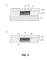
- FIG. 4(A) shows an alternative embodiment, which is similar to the embodiment shown in FIGS. 1-3 except that a through-hole 50 is formed on the glass substrate 22 B and buffer 52 is disposed between the embedded piezo vibration element 40 and the touch panel 20 .
- the embedded piezo vibration element 40 is supported by the touch panel 20 via the buffer 52 .
- the buffer 52 may have a modulus of elasticity of 10-100 MPa. The buffer 52 may prevent the touch panel 20 from interrupting the transmission of the vibration from the piezo vibration element 40 to the protective panel 22 .
- FIG. 4(B) shows an alternative embodiment, which is similar to the embodiment shown in FIGS. 1-3 except that the glass substrate 22 B has recess(es) (or stepped portion) 60 having a pair of tapered walls 62 extending upwardly at an angle of approximately 20° with respect to the vertical, instead of the recesses 30 A and 30 B.
- the piezo vibration element 40 may be mounted within the recess 60 .
- the tapered shape of the recess 60 may enhance efficiency of vibration transmission.
- the transparent protective panel 22 for protecting the display unit 18 and touch panel 20 is configured by joining two glass substrates 22 A and 22 B; and the recesses 30 A and 30 B (or through-hole 50 or recess 60 ) are formed in the glass substrate 22 B disposed on the touch panel 20 side from the surface facing the glass substrate 22 A such that the depth of each of the recesses 30 A and 30 B is greater than the thickness of the corresponding piezo vibration element 40 , wherein the piezo vibration elements 40 are disposed within the recesses 30 A and 30 B (or through-hole 50 or recess 60 ) and joined with the glass substrate 22 A.
- each of the vibrations generated by the piezo vibration elements 40 may be transmitted as a surface elastic wave to the front surface of the protective panel 22 , thereby vibrating the front surface of the protective panel 22 sufficiently to convey an enhanced sensory perception to a user's finger even with a small displacement and actuator force.
- the touch panel device according to the present disclosure may provide sufficient haptic effects while maintaining a low-profile configuration.
- the piezo vibration element 40 can be disposed without overlapping the touch panel 20 . This way, the touch panel 20 does not inhibit the vibration generated by the piezo vibration elements 40 .
- the glass substrate 22 A residing on the front surface side is formed thinner than the glass substrate 22 B residing on the touch panel side, thereby efficiently conveying the vibration generated by each of the piezo vibration elements 40 with a smaller actuator force.
- the touch panel device according to one embodiment is provided with two separate piezo vibration elements 40 that can be controlled by separate input signals each having different amplitudes and phases from one another. Those separate signals may control corresponding piezo vibration elements 40 respectively and independently so as to selectively vibrate an area contacted by a user's finger by, for example, generating a stronger vibration at a particular position.
- the piezo vibration element 40 may be formed rectangular in plan view and mounted on the recesses 30 A and 30 B (or through-hole 50 or recess 60 ) stiffly at the both ends thereof while flexibly at the mid portions thereof, thereby efficiently conveying the generated vibrations to the glass substrate 22 .
- the piezo vibration element 40 is configured by alternately laminating a plurality of piezoelectric layers 42 and a plurality of electrode layers 44 so that it can operate with a lower input voltage.
- the piezo vibration element 40 is configured to have a bimorph structure which may generate larger displacement or actuator force.
- the piezo vibration element 40 may be formed rectangular but the particular shapes and sizes described above are not limiting. Rather, the piezo vibration element 40 may be configured to have any length, width, and thickness within the spirit and scope of the present invention.
- the piezo vibration element 40 may be formed annular.
- a transparent protective substrate for protecting a display unit and touch panel is configured by joining first and second glass substrates, wherein either the first or second glass substrate is formed to have one or more stepped portions on their facing surfaces such that the stepped portions may be formed thicker than the corresponding piezo vibration element.
- the first and second glass substrates are joined while maintaining each of the piezo vibration elements within the corresponding stepped portion.
- a small vibration or displacement may be transmitted to the front surface of the protective substrate in such a manner as to sufficiently provide haptic effects to a user via the protective substrate.
- various embodiments of the present disclosure may be applied to various touch panel devices or electronic devices having the same.
- the touch panel devices may be implemented in various low-profile devices for enhanced haptic effects.
Landscapes
- Engineering & Computer Science (AREA)
- General Engineering & Computer Science (AREA)
- Theoretical Computer Science (AREA)
- Human Computer Interaction (AREA)
- Physics & Mathematics (AREA)
- General Physics & Mathematics (AREA)
- Computer Hardware Design (AREA)
- Position Input By Displaying (AREA)
- User Interface Of Digital Computer (AREA)
Abstract
Description
- This application is based upon and claims the benefit of priority from prior Japanese Patent Application 2011-071250 filed on Mar. 28, 2011 titled “touch panel device and electronic device,” the entire contents of which are incorporated herein by reference.
- The present disclosure relates to a touch panel device, and more particularly to a touch panel device with a force feedback function (or haptic function) using a piezo vibration element. The present disclosure also relates to an electronic device having such a touch panel device.
- Electronic devices such as mobile phones use a touch sensitive switch. Such a touch sensitive switch may comprise a display panel such as liquid crystal panel and a pressure sensitive or capacitance type input device. Such touch sensitive switches tend to have a shorter stroke than ordinary mechanical switches. Users sometimes cannot perceive such a short stroke. Hence, developments have been made to provide touch panel devices that can produce vibration or other mechanical movements in concert with a push-down operation by a user so that the user can recognize that their push-down operation was actually made.
- Haptic feedback can be generated by various conventional driving sources including a piezoelectric actuator, as described in Japanese Patent Application Publication No. 2010-157037, and an electromagnetic actuator, as described in Japanese Patent Application Publication No. 2006-146611. These actuators are disposed on non-displaying areas of a display panel so as to provide vibration without preventing a user from viewing displayed images on the display panel. Haptic feedbacks can also be provided by other conventional configurations, such as a structure configured by stacking a liquid crystal panel, touch panel, and haptic panel, as described in Japanese Patent Application Publication No. 2011-2926. A haptic actuator can be disposed beneath a liquid crystal panel, as described in Japanese Patent Application Publication No. 2010-152889.
- In such conventional haptic feedback devices, in response to a user's pressure contact with a touch panel, an actuator is configured to deform such that the deformation can be conveyed from the touch panel to the user's finger so as to provide the user with a sense that the user made sufficiently contact with the touch panel. An input signal to such an actuator can be a simple sinusoidal signal or square wave signal. A special signal such as a kick-in pulse or braking pulse also can be used as an input signal, as described in Japanese Patent Application Publication No. 2010-287231. An actuator signal is also input to an actuator to cause the entire panel to vibrate and operate as a speaker for reproducing a recorded sound of music or voice.
- However, in those conventional haptic mechanisms described in the above references, a haptic actuator is disposed on the bottom or rear surface of a heavy liquid crystal panel or touch panel. This arrangement requires an actuator to generate a large actuator force and displacement in order to provide sufficient haptic effects. To achieve such a large actuator force and displacement, a high voltage input needs to be applied. Such a high voltage is difficult to use in electronic devices such as mobile phones. Moreover, an actuator is needed separately from the liquid crystal panel and touch panel. Therefore, the resulting display device become thicker and cannot be made thin.
- The present disclosure provides a low-profile touch panel device and electronic device for providing enhanced haptic effects by effectively transmitting vibration generated by an actuator with relatively small force output and small displacement to the front surface of the touch panel device.
- Additional or separate features and advantages of the invention will be set forth in the descriptions that follow and in part will be apparent from the description, or may be learned by practice of the invention. The objectives and other advantages of the invention will be realized and attained by the structure particularly pointed out in the written description and claims thereof as well as the appended drawings.
- To achieve these and other advantages and in accordance with the purpose of the present invention, as embodied and broadly described, in one aspect, the present invention provides a touch panel device including a touch panel; a display unit disposed on a rear side of the touch panel; a transparent protective substrate disposed on a front side of the touch panel, the protective substrate being configured by joining a first glass substrate residing on a front side and a second glass substrate residing on a touch panel side, wherein either one of the first and second glass substrates is configured to have one or more stepped portions formed either on a rear surface of the first glass substrate or a front surface of the second glass substrate, the rear surface of the first glass substrate and the front surface of the second glass substrate facing one another; and one or more piezo vibration elements each disposed within one of the stepped portions so as to be acoustically coupled with the first glass substrate, wherein each of said one or more stepped portions is configured thicker than the corresponding piezo vibration element.
- In one aspect, at least one of the stepped portions is formed on the second glass substrate. In another aspect, at least one of the stepped portions is formed as a through-hole. In yet another aspect, one or more buffers are disposed between one of the piezo vibration elements and the touch panel. In further still another aspect, the first glass substrate is configured thinner than the second glass substrate. In another aspect, the at least one of the stepped portions is formed to have a tapered wall configured such that a cross section of said at least one of the stepped portions becomes wider as approaching the first glass substrate. In another aspect, at least one of the piezo vibration elements includes a plurality of piezoelectric layers and a plurality of electrode layers laminated in an alternate manner. In another aspect, at least one of the piezo vibration elements has a bimorph structure. In yet another aspect, each of vibrations generated by the piezo vibration elements is conveyed to the first glass substrate in a form of a surface elastic wave.
- In one aspect, an electronic device according to the present disclosure comprises one of the above-described touch panel devices. In addition to the illustrative aspects, embodiments, and features described above, further aspects, embodiments, and features will become apparent by reference to the drawings and the following detailed description.
- According to the present disclosure, a transparent protective substrate for protecting a display unit and touch panel is configured by joining the first and second glass substrates, wherein either the first or second glass substrate is formed to have one or more stepped portions on their joined surface side thickness so as to be thicker than the piezo vibration element. The first and second glass substrates are joined such that the piezo vibration element is embedded within the stepped portion. Thus, even a small vibration or displacement generated by the piezo vibration element may be transmitted to the protective substrate front surface in such a manner as to sufficiently provide haptic effects to a user.
- It is to be understood that both the foregoing general description and the following detailed description are exemplary and explanatory, and are intended to provide further explanation of the invention as claimed.
-
FIG. 1 shows an electronic device in accordance with one embodiment of the present disclosure, and more particularly,FIG. 1(A) shows a perspective view of the electronic device; andFIG. 1(B) shows an exploded perspective view of a panel display unit of the electronic device. -
FIG. 2 shows a cross section of a piezo vibration element mounting portion viewed from arrow #A inFIG. 1(A) . -
FIG. 3 shows a cross section of a piezo vibration element viewed from arrow #B inFIG. 1(B) . -
FIG. 4 shows another embodiment of the present disclosure. - Embodiments of the present disclosure will be described below.
- With reference to
FIGS. 1-3 , one embodiment of the present disclosure will be described. The present disclosure relates to technologies for providing haptic effects for various electronic devices that include a display unit and touch panel device associated therewith. Those electronic devices include mobile phones, smartphones, car navigation devices and game consoles, but those devices are not limiting. Such haptic effects are provided to a user for sensory perception during input operation.FIG. 1 shows a smartphone as an example of an electronic device in accordance with one aspect of the present disclosure. - As shown in
FIGS. 1 and 2 ,smartphone 10 in accordance with one embodiment includes adisplay unit 18 and atouch panel 20 housed within astorage portion 14 of ahousing 12. The almost entire front surface of thesmartphone 10 is covered by a transparent protective panel 22 (protective substrate). Theprotective panel 22 is supported by anedge 16 of thehousing 12. The term “transparent” is intended to describe the fact that images displayed on the display unit is visible to a user through the protective substrate although the display unit is disposed rear of the protective substrate. Theprotective panel 22 is provided with anopening 24 for a receiver and anopening 28 for anoperation switch 26. Adisplay area 46 on which images are displayed exists in a specific area around the center of theprotective panel 22. Theprotective panel 22 is a joined substrate configured by joining afirst glass substrate 22A disposed on the front surface side and asecond glass substrate 22B disposed on thetouch panel 20 side. The first andsecond glass substrates - The
touch panel 20 is disposed on the lower side (or rear side) of theprotective panel 22. Thetouch panel 20 may be any type of known touch panel device including a capacitance type touch panel and a resistive touch display. Thedisplay unit 18 is disposed beneath thetouch panel 20. Thedisplay unit 18 may be a liquid crystal display device, an organic EL, or any type of known display devices. Theprotective panel 22 is fixed to thetouch panel 20 via, for example, an optically transparent glue (not shown) or adhesive tape (not shown). Thetouch panel 20 is also fixed to thedisplay unit 18 in the same manner. The glue may include epoxy or any other ordinary bonding material. The adhesive material may include acrylic adhesive or any other ordinary adhesive materials. - The illustrated
protective panel 22 is provided with a pair ofpiezo vibration elements 40. In the illustrated embodiment, thelower glass substrate 22B is provided with a pair of steppedportions recesses piezo vibration elements 40. Although the illustrated touch panel device has a pair ofpiezo vibration elements 40, the number ofpiezo vibration elements 40 is not limited, but any number ofpiezo vibration elements 40 may be used depending on a particular configuration of an electronic device on which the touch panel device is mounted. For example, a singlepiezo vibration element 40 or threepiezo vibration elements 40 may be mounted on a touch panel device. Therecesses glass substrate 22B on its front surface side. The height of the steppedportions recesses piezo vibration elements 40. The thickness of thepiezo vibration element 40 refers to the sum of at least the thickness of thepiezo vibration element 40 without deformation and the amount of the possible displacement of thepiezo vibration element 40. The upper surface of each of thepiezo vibration elements 40 is attached to theupper glass substrate 22A via a glue, adhesive, or double-faced tape; and the lower surface of thepiezo vibration elements 40 is supported on the bottom surfaces of therecesses piezo vibration elements 40 is formed rectangular in plan view. Thepiezo vibration elements 40 may be mounted on therecesses corresponding recesses glass substrate 22. Preferably, the peripheral portions (or both ends) of thepiezo vibration elements 40 are attached to thecorresponding recesses recesses piezo vibration elements 40. - The thickness of the
protective panel 22 including theglass substrates protective panel 22 is mounted, but is preferably less than 1 mm. In the illustrated embodiment, theupper glass substrate 22A is formed thinner than thelower glass substrate 22B so as to effectively convey the vibrations generated with a smaller actuator force. As shown inFIG. 2 , each of thepiezo vibration elements 40 is disposed such that it does not face thetouch panel 20 in plan view, thereby preventing thetouch panel 20 from interrupting the vibration of thepiezo vibration elements 40. - Next, with reference to
FIG. 3 , thepiezo vibration elements 40 will be described in further detail. As shown inFIG. 3 , thepiezo vibration element 40 is configured by alternately stacking a plurality ofpiezoelectric layers 42 and electrode layers 44. Thepiezo vibration elements 40 in the illustrated embodiment may be a bimorph piezoelectric vibrator wherein theupper portion 40A and thelower portion 40B have different polarization directions therebetween. Alternatively, thepiezo vibration element 40 may alternatively have either a single plate structure or a unimorph structure. If thepiezo vibration element 40 is a unimorph type element, all the piezoelectric layers forming theelement 40 are polarized in the same direction depending on a particular arrangement of the electronic device on which thepiezo vibration element 40 is mounted. The laminated structure is preferable because it can operate with a lower voltage input. In addition, the bimorph structure is preferable if larger displacement or actuator force is desired. Thepiezoelectric layers 42 may be made of various piezoelectric ceramics known to a person skilled in the art such as lead zirconate titanate with appropriate additives. The electrode layers 44 may be made of various electrode materials including silver or platinum. Those materials for thepiezoelectric layers 42 andelectrode layers 44 are not limiting, but any suitable materials may be used. - Each of the
piezo vibration elements 40 is embedded within theglass substrate 22B. Each of thepiezo vibration elements 40 is preferably configured thick enough to convey the generated displacement or actuator force and to function as the protective panel. Accordingly, the thickness of each of thepiezo vibration elements 40 may be in the range of 0.4 mm-0.6 mm in one embodiment. The suitable width and length of thepiezo vibration elements 40 may depend on the electronic device on which theelement 40 is mounted. In the case of the illustratedsmartphone 10, the dimensions preferably are the length of 60 mm or less and the width of 5 mm or less. The width of more than 2 mm is more preferable so as to sufficiently convey the generated vibration to the glass surface. In the illustrated embodiment, thepiezo vibration elements 40 may be configured to have the thickness of 0.5 mm, the length of 50 mm, and the width of 3 mm. The thickness of each of the illustratedpiezoelectric layers 42 may be 18 μm and thepiezo vibration elements 40 may have 26 layers of thepiezoelectric layer 42. The number of laminatedpiezoelectric layers 42 is not limited, and any number ofpiezoelectric layers 42 may be used to form thepiezo vibration element 40. - One of the electrode layers 44 may be formed on the front surface of each of the
piezo vibration elements 40 and connected to a driving circuit (not shown). Conducting paths for connecting theelectrode layer 44 with the driving circuit may be formed on the front surface of theglass substrates 22A and/or 22B by printing or sputtering, for example. The conducting path may also be formed of ultrafine metal lines. A touch panel device (or a panel display unit thereof) for providing haptic effects in accordance with the present disclosure may be fabricated by laminating theabove display unit 18, thetouch panel 20, and theprotective panel 22 having thepiezo vibration elements 40. - In operation, in response to a pressure contact by a user with the
protective panel 22 at an area corresponding to an image displayed on thedisplay area 46, it is detected that thetouch panel 20 is pressed down. Upon detection of the press-down operation, a signal is supplied to one or more of thepiezo vibration elements 40 for activation. Since the glass surrounding (or the glass on the lateral sides of) thepiezo vibration elements 40 is thicker and more rigid than the glass on the upper side (i.e., theglass substrate 22A) of the same, each of the vibrations generated by thepiezo vibration elements 40 in therecesses glass substrate 22B is transmitted in the form of a surface elastic wave and is conveyed to the finger or the pen tip of a stylus that pressed theprotective panel 22. Thus, enhanced perception that a switch was sufficiently pressed can be conveyed to a user with a smaller actuator force as compared to a conventional arrangement in which a generated vibration is conveyed through the entire thickness of the glass substrate (protective panel 22). - The signal input to each of the
piezo vibration elements 40 may be a simple sinusoidal signal, square wave signal or combination thereof. The signal may also be any signal disclosed in Japanese Patent Application Publication No. 2010-287231, which is incorporated in its entirety herein by reference, such as a kick-in pulse or braking pulse. In the illustrated embodiments, the amplitude or phase of each of the input signals to the pair ofpiezo vibration elements 40 may be controlled such that a strong vibration can be generated in a particular area in theprotective panel 22. The signal may also be controlled so as to selectively vibrate an area contacted by a user's finger. - The amount of displacement of the
protective panel 22 of the touch panel device in accordance with one embodiment (panel display unit) was measured using a 200 Hz, 8 Vrms input signal. A human's finger is the most sensitive to a 200 Hz vibration. In addition, an acoustic pressure of the sound generated by the same touch panel device was measured via a microphone disposed 10 cm away from the front surface of theprotective panel 22 using a 100 Hz sinusoidal input signal. The measured amount of displacement was 4 μm and the measured acoustic pressure was 90 dB. Another touch panel device was prepared as a comparative example. The comparative touch panel device was provided with a pair of piezo vibration elements that are disposed beneath a display device. The amount of displacement and acoustic pressure of the sound generated by the comparative touch panel device was measured. The measured displacement for the comparative touch panel device was 0.3 μm and the measured acoustic pressure was 70 dB. Thus, it was found that the amount of displacement and the acoustic pressure generated by the touch panel device in accordance with one embodiment of the present disclosure were significantly improved. - Now, with reference to
FIG. 4 , other embodiments of the present disclosure will be described.FIG. 4(A) shows an alternative embodiment, which is similar to the embodiment shown inFIGS. 1-3 except that a through-hole 50 is formed on theglass substrate 22B andbuffer 52 is disposed between the embeddedpiezo vibration element 40 and thetouch panel 20. Thus, the embeddedpiezo vibration element 40 is supported by thetouch panel 20 via thebuffer 52. Thebuffer 52 may have a modulus of elasticity of 10-100 MPa. Thebuffer 52 may prevent thetouch panel 20 from interrupting the transmission of the vibration from thepiezo vibration element 40 to theprotective panel 22. -
FIG. 4(B) shows an alternative embodiment, which is similar to the embodiment shown inFIGS. 1-3 except that theglass substrate 22B has recess(es) (or stepped portion) 60 having a pair of taperedwalls 62 extending upwardly at an angle of approximately 20° with respect to the vertical, instead of therecesses piezo vibration element 40 may be mounted within therecess 60. The tapered shape of therecess 60 may enhance efficiency of vibration transmission. - The above-described touch panel device in accordance with various embodiments provides the following advantageous effects:
- (1) In one embodiment, the transparent
protective panel 22 for protecting thedisplay unit 18 andtouch panel 20 is configured by joining twoglass substrates recesses hole 50 or recess 60) are formed in theglass substrate 22B disposed on thetouch panel 20 side from the surface facing theglass substrate 22A such that the depth of each of therecesses piezo vibration element 40, wherein thepiezo vibration elements 40 are disposed within therecesses hole 50 or recess 60) and joined with theglass substrate 22A. Accordingly, each of the vibrations generated by thepiezo vibration elements 40 may be transmitted as a surface elastic wave to the front surface of theprotective panel 22, thereby vibrating the front surface of theprotective panel 22 sufficiently to convey an enhanced sensory perception to a user's finger even with a small displacement and actuator force. Thus, the touch panel device according to the present disclosure may provide sufficient haptic effects while maintaining a low-profile configuration. - (2) Because the bottom surface of the
recesses glass substrate 22B supports thepiezo vibration elements 40, thepiezo vibration element 40 can be disposed without overlapping thetouch panel 20. This way, thetouch panel 20 does not inhibit the vibration generated by thepiezo vibration elements 40. (3) Theglass substrate 22A residing on the front surface side is formed thinner than theglass substrate 22B residing on the touch panel side, thereby efficiently conveying the vibration generated by each of thepiezo vibration elements 40 with a smaller actuator force. (4) The touch panel device according to one embodiment is provided with two separatepiezo vibration elements 40 that can be controlled by separate input signals each having different amplitudes and phases from one another. Those separate signals may control correspondingpiezo vibration elements 40 respectively and independently so as to selectively vibrate an area contacted by a user's finger by, for example, generating a stronger vibration at a particular position. - (5) The
piezo vibration element 40 may be formed rectangular in plan view and mounted on therecesses hole 50 or recess 60) stiffly at the both ends thereof while flexibly at the mid portions thereof, thereby efficiently conveying the generated vibrations to theglass substrate 22. (6) In one embodiment, thepiezo vibration element 40 is configured by alternately laminating a plurality ofpiezoelectric layers 42 and a plurality of electrode layers 44 so that it can operate with a lower input voltage. (7) In one embodiment, thepiezo vibration element 40 is configured to have a bimorph structure which may generate larger displacement or actuator force. - The foregoing illustrated embodiments have been provided solely to illustrate the structural and functional principles of the present invention, and should not be regarded as limiting. To the contrary, the present invention is intended to encompass all modifications, substitutions, and alterations within the spirit and scope of the following claims. For example, the sizes and shapes of various components of the touch panel devices in accordance with various embodiments may vary. As noted above, the
piezo vibration element 40 may be formed rectangular but the particular shapes and sizes described above are not limiting. Rather, thepiezo vibration element 40 may be configured to have any length, width, and thickness within the spirit and scope of the present invention. For example, thepiezo vibration element 40 may be formed annular. - According to the above-described embodiments of the present disclosure, a transparent protective substrate for protecting a display unit and touch panel is configured by joining first and second glass substrates, wherein either the first or second glass substrate is formed to have one or more stepped portions on their facing surfaces such that the stepped portions may be formed thicker than the corresponding piezo vibration element. The first and second glass substrates are joined while maintaining each of the piezo vibration elements within the corresponding stepped portion. Thus, even a small vibration or displacement may be transmitted to the front surface of the protective substrate in such a manner as to sufficiently provide haptic effects to a user via the protective substrate. As such, various embodiments of the present disclosure may be applied to various touch panel devices or electronic devices having the same. The touch panel devices may be implemented in various low-profile devices for enhanced haptic effects.
Claims (10)
Applications Claiming Priority (2)
| Application Number | Priority Date | Filing Date | Title |
|---|---|---|---|
| JP2011071250A JP5597583B2 (en) | 2011-03-28 | 2011-03-28 | Touch panel device and electronic device |
| JP2011-071250 | 2011-03-28 |
Publications (2)
| Publication Number | Publication Date |
|---|---|
| US20120249459A1 true US20120249459A1 (en) | 2012-10-04 |
| US8884897B2 US8884897B2 (en) | 2014-11-11 |
Family
ID=46926541
Family Applications (1)
| Application Number | Title | Priority Date | Filing Date |
|---|---|---|---|
| US13/431,619 Active 2032-08-11 US8884897B2 (en) | 2011-03-28 | 2012-03-27 | Touch panel device and electronic device with improved haptic feedback |
Country Status (2)
| Country | Link |
|---|---|
| US (1) | US8884897B2 (en) |
| JP (1) | JP5597583B2 (en) |
Cited By (33)
| Publication number | Priority date | Publication date | Assignee | Title |
|---|---|---|---|---|
| US20140232679A1 (en) * | 2013-02-17 | 2014-08-21 | Microsoft Corporation | Systems and methods to protect against inadvertant actuation of virtual buttons on touch surfaces |
| US20140230575A1 (en) * | 2013-02-17 | 2014-08-21 | Microsoft Corporation | Piezo-actuated virtual buttons for touch surfaces |
| US8884897B2 (en) * | 2011-03-28 | 2014-11-11 | Taiyo Yuden Co., Ltd. | Touch panel device and electronic device with improved haptic feedback |
| US20150062458A1 (en) * | 2012-03-29 | 2015-03-05 | Kyocera Corporation | Input device, display device, and electronic device |
| DE102014000829A1 (en) * | 2014-01-21 | 2015-07-23 | Harald Kobolla | Portable computer with a haptic output device |
| US20150247765A1 (en) * | 2013-01-18 | 2015-09-03 | Murata Manufacturing Co., Ltd. | Displacement detection sensor and operation input device |
| CN105378613A (en) * | 2013-07-11 | 2016-03-02 | 太阳诱电株式会社 | Vibration device and electronic device using same |
| US20160127524A1 (en) * | 2013-07-18 | 2016-05-05 | Kyocera Corporation | Electronic apparatus |
| WO2016093414A1 (en) * | 2014-12-09 | 2016-06-16 | 엘지전자 주식회사 | Sensor-actuator for touch input apparatus, and terminal apparatus using same |
| US9448631B2 (en) | 2013-12-31 | 2016-09-20 | Microsoft Technology Licensing, Llc | Input device haptics and pressure sensing |
| US9451069B2 (en) | 2012-12-25 | 2016-09-20 | Kyocera Corporation | Mobile terminal device, lock release method, and non-transitory computer readable storage medium |
| US9459160B2 (en) | 2012-06-13 | 2016-10-04 | Microsoft Technology Licensing, Llc | Input device sensor configuration |
| US9621700B2 (en) | 2012-12-25 | 2017-04-11 | Kyocera Corporation | Mobile terminal device |
| US9696891B2 (en) | 2012-12-25 | 2017-07-04 | Kyocera Corporation | Mobile terminal device, screen control method, and non-transitory computer readable storage medium |
| CN107506092A (en) * | 2017-09-30 | 2017-12-22 | 联想(北京)有限公司 | A kind of input control method and terminal |
| US20180070180A1 (en) * | 2016-09-08 | 2018-03-08 | Microsoft Technology Licensing, Llc | Display structure having a visual display and an audio output |
| US9949036B2 (en) | 2013-12-26 | 2018-04-17 | Kyocera Corporation | Electronic device |
| US10061385B2 (en) | 2016-01-22 | 2018-08-28 | Microsoft Technology Licensing, Llc | Haptic feedback for a touch input device |
| JP2018169809A (en) * | 2017-03-30 | 2018-11-01 | 京セラディスプレイ株式会社 | Display |
| US10162466B2 (en) | 2014-01-29 | 2018-12-25 | Kyocera Corporation | Portable device and method of modifying touched position |
| US20190050024A1 (en) * | 2017-08-10 | 2019-02-14 | Samsung Display Co. Ltd. | Display panel, bracket and display device including the same |
| US10222889B2 (en) | 2015-06-03 | 2019-03-05 | Microsoft Technology Licensing, Llc | Force inputs and cursor control |
| US10228770B2 (en) | 2012-06-13 | 2019-03-12 | Microsoft Technology Licensing, Llc | Input device configuration having capacitive and pressure sensors |
| US10265826B2 (en) | 2013-06-07 | 2019-04-23 | 3M Innovative Properties Company | Method of forming a recess in a substrate |
| US10416799B2 (en) | 2015-06-03 | 2019-09-17 | Microsoft Technology Licensing, Llc | Force sensing and inadvertent input control of an input device |
| US20190339779A1 (en) * | 2017-01-04 | 2019-11-07 | Hap2U | Vibrating tactile tile |
| CN110869233A (en) * | 2017-07-13 | 2020-03-06 | 宝马股份公司 | Display device and motor vehicle with display device |
| CN111124127A (en) * | 2019-12-25 | 2020-05-08 | 吉林大学 | Digital key touch rendering method and device based on vibration and squeeze film effect |
| CN111602106A (en) * | 2018-01-22 | 2020-08-28 | 株式会社丸和制作所 | Tactile sensation imparting device and program |
| JP2021028802A (en) * | 2019-08-09 | 2021-02-25 | Tdk株式会社 | Vibration unit |
| US20210060611A1 (en) * | 2019-08-29 | 2021-03-04 | Taiyo Yuden Co., Ltd. | Vibration panel and electronic apparatus |
| US11466672B2 (en) * | 2018-01-22 | 2022-10-11 | Maruwa Corporation | Actuator |
| US11978276B2 (en) | 2020-05-13 | 2024-05-07 | Samsung Electronics Co., Ltd. | Electronic device comprising optical sensor module |
Families Citing this family (18)
| Publication number | Priority date | Publication date | Assignee | Title |
|---|---|---|---|---|
| US8405618B2 (en) * | 2006-03-24 | 2013-03-26 | Northwestern University | Haptic device with indirect haptic feedback |
| JP5926950B2 (en) * | 2011-12-22 | 2016-05-25 | 京セラ株式会社 | Electronics |
| JP5909682B2 (en) * | 2012-10-09 | 2016-04-27 | パナソニックIpマネジメント株式会社 | Electronics |
| JP5960587B2 (en) * | 2012-12-19 | 2016-08-02 | 京セラ株式会社 | Input device, display device, and electronic device |
| JP6133619B2 (en) * | 2013-02-22 | 2017-05-24 | 京セラ株式会社 | Vibration device, electronic device, and portable terminal |
| JP6001482B2 (en) * | 2013-03-25 | 2016-10-05 | 京セラ株式会社 | Input device and electronic device |
| JP2015005426A (en) * | 2013-06-21 | 2015-01-08 | 株式会社東芝 | Nonaqueous electrolyte battery |
| WO2014208691A1 (en) | 2013-06-26 | 2014-12-31 | 京セラ株式会社 | Portable device and method for controlling portable device |
| JP5815612B2 (en) * | 2013-07-29 | 2015-11-17 | 京セラ株式会社 | Electronics |
| CN105378614B (en) * | 2013-08-06 | 2019-05-21 | 株式会社村田制作所 | Pressing detection sensors |
| CN105765750B (en) * | 2013-11-21 | 2018-07-20 | 3M创新有限公司 | multi-layer piezoelectric polymer film device and method |
| JP6272022B2 (en) * | 2013-12-26 | 2018-01-31 | 京セラ株式会社 | Electronics |
| JP2015153406A (en) * | 2014-02-19 | 2015-08-24 | Fdk株式会社 | tactile transmission device |
| JP6360367B2 (en) | 2014-06-26 | 2018-07-18 | 京セラ株式会社 | Portable electronic device, control method and program for portable electronic device |
| JP2016080465A (en) * | 2014-10-15 | 2016-05-16 | 日本写真印刷株式会社 | Pressure detector |
| JP6062519B1 (en) | 2015-09-28 | 2017-01-18 | 京セラ株式会社 | Electronic device and method of operating electronic device |
| DE102015226321A1 (en) | 2015-12-21 | 2017-06-22 | Zf Friedrichshafen Ag | Gear selector switch for a motor vehicle and method for detecting actuation of a gear selector switch for a motor vehicle |
| JP6143838B2 (en) * | 2015-12-24 | 2017-06-07 | 京セラ株式会社 | Electronics |
Citations (35)
| Publication number | Priority date | Publication date | Assignee | Title |
|---|---|---|---|---|
| US6087198A (en) * | 1998-02-12 | 2000-07-11 | Texas Instruments Incorporated | Low cost packaging for thin-film resonators and thin-film resonator-based filters |
| US6205226B1 (en) * | 1998-06-22 | 2001-03-20 | Hokuriku Electric Industry Co., Ltd. | Piezoelectric acoustic device |
| US20040232802A1 (en) * | 2002-07-31 | 2004-11-25 | Yoshihiro Koshido | Piezoelectric component and method for manufacturing the same |
| US20050035685A1 (en) * | 2002-11-13 | 2005-02-17 | Elo Touchsystems, Inc. | Acoustic wave touch detecting apparatus |
| US20060097996A1 (en) * | 2004-11-10 | 2006-05-11 | Alps Electric Co., Ltd. | Input device |
| US7184027B2 (en) * | 2000-10-13 | 2007-02-27 | Denso Corporation | Touch panel, display device and method of producing touch panel |
| US7199788B2 (en) * | 2002-10-04 | 2007-04-03 | Smk Corporation | Pointing input device |
| US7242395B2 (en) * | 2003-03-10 | 2007-07-10 | Fujitsu Component Limited | Input device and driving device thereof |
| US7439824B2 (en) * | 2004-03-09 | 2008-10-21 | Infineon Technologies Ag | Bulk acoustic wave filter and method for eliminating unwanted side passbands |
| US20080315717A1 (en) * | 2005-10-26 | 2008-12-25 | Martin Schroder | Piezoelectric Actuator and Method for Producing the Same |
| US20090267902A1 (en) * | 2005-09-21 | 2009-10-29 | Smk Corporation | Touch Panel |
| US20090284485A1 (en) * | 2007-03-21 | 2009-11-19 | Northwestern University | Vibrating substrate for haptic interface |
| US20100141580A1 (en) * | 2007-08-22 | 2010-06-10 | Oh Eui Jin | Piezo-electric sensing unit and data input device using piezo-electric sensing |
| US20100231550A1 (en) * | 2009-03-12 | 2010-09-16 | Immersion Corporation | Systems and Methods for Friction Displays and Additional Haptic Effects |
| US20100253648A1 (en) * | 2009-04-06 | 2010-10-07 | 3M Innovative Properties Company | Touch sensor with modular sensing components |
| US20100277439A1 (en) * | 2009-04-30 | 2010-11-04 | Motorola, Inc. | Dual Sided Transparent Display Module and Portable Electronic Device Incorporating the Same |
| US20100295807A1 (en) * | 2009-05-19 | 2010-11-25 | Beijing Boe Optoelectronics Technology Co., Ltd. | Touch screen, color filter substrate and manufacturing methods thereof |
| US20100321330A1 (en) * | 2009-06-19 | 2010-12-23 | Samsung Electronics Co., Ltd. | Touch panel and electronic device including the same |
| US20110050406A1 (en) * | 2009-04-02 | 2011-03-03 | Pi Ceramic Gmbh | Device for producing a haptic feedback from a keyless input unit |
| US20110050604A1 (en) * | 2009-09-02 | 2011-03-03 | Kwon Do-Hyun | Organic light emitting display apparatus |
| US20110096013A1 (en) * | 2009-01-08 | 2011-04-28 | Krumpelman Douglas M | Techniques for tactile feedback technology |
| US20110102342A1 (en) * | 2009-11-02 | 2011-05-05 | Smk Corporation | Holding structure for a touch panel |
| US20110148795A1 (en) * | 2008-12-22 | 2011-06-23 | Kyocera Corporation | Input apparatus |
| US20110242055A1 (en) * | 2010-04-02 | 2011-10-06 | Samsung Electronics Co., Ltd. | Composite touch screen panel |
| US20110248788A1 (en) * | 2009-02-25 | 2011-10-13 | Youichi Fujihira | Glass substrate polishing method, package manufacturing method, piezoelectric vibrator, oscillator, electronic device and radio timepiece |
| US20110261021A1 (en) * | 2010-04-23 | 2011-10-27 | Immersion Corporation | Transparent composite piezoelectric combined touch sensor and haptic actuator |
| US20110260585A1 (en) * | 2010-04-27 | 2011-10-27 | Nihon Dempa Kogyo Co., Ltd. | Surface-mountable piezoelectric devices including eutectic-bonded packages |
| US20120075221A1 (en) * | 2010-09-27 | 2012-03-29 | Stanley Electric Co., Ltd. | Touchscreen panel input device manufacturing method, piezoelectric element and touchscreen panel input device |
| US20120105400A1 (en) * | 2010-10-29 | 2012-05-03 | Mathew Dinesh C | Camera lens structures and display structures for electronic devices |
| US20120105333A1 (en) * | 2010-11-02 | 2012-05-03 | Apple Inc. | Methods and systems for providing haptic control |
| US20120113031A1 (en) * | 2010-11-10 | 2012-05-10 | Sunghoon Lee | Electrophoresis display having touch screen and method for driving the touch screen |
| US20120223543A1 (en) * | 2005-10-13 | 2012-09-06 | Magna International, Inc. | Acoustical window assembly for vehicle |
| US8467177B2 (en) * | 2010-10-29 | 2013-06-18 | Apple Inc. | Displays with polarizer windows and opaque masking layers for electronic devices |
| US8576186B2 (en) * | 2009-11-02 | 2013-11-05 | Smk Corporation | Holding structure for a touch panel |
| US8717314B2 (en) * | 2009-11-02 | 2014-05-06 | Smk Corporation | Holding structure for a touch panel |
Family Cites Families (13)
| Publication number | Priority date | Publication date | Assignee | Title |
|---|---|---|---|---|
| JP2001218001A (en) * | 2000-02-04 | 2001-08-10 | Ricoh Co Ltd | Original reader |
| JP4527315B2 (en) * | 2001-05-14 | 2010-08-18 | セイコーインスツル株式会社 | Display device |
| JP3834494B2 (en) * | 2001-09-19 | 2006-10-18 | 株式会社ケンウッド | Piezoelectric speaker device |
| JP2004125571A (en) * | 2002-10-01 | 2004-04-22 | National Institute Of Advanced Industrial & Technology | Transparent piezoelectric sensor and input device having the same |
| JP2006146611A (en) | 2004-11-19 | 2006-06-08 | Fujitsu Component Ltd | Haptic panel device |
| JP2007065800A (en) * | 2005-08-29 | 2007-03-15 | Seiko Epson Corp | Touch panel device |
| EP2202619A1 (en) | 2008-12-23 | 2010-06-30 | Research In Motion Limited | Portable electronic device including tactile touch-sensitive input device and method of controlling same |
| JP2010157037A (en) | 2008-12-26 | 2010-07-15 | Nissha Printing Co Ltd | Panel member having oscillating element |
| KR101885740B1 (en) * | 2009-03-12 | 2018-08-06 | 임머숀 코퍼레이션 | Systems and methods for providing features in a friction display |
| JP5343871B2 (en) * | 2009-03-12 | 2013-11-13 | 株式会社リコー | Touch panel device, display device with touch panel including the same, and control method for touch panel device |
| US10401961B2 (en) | 2009-06-09 | 2019-09-03 | Immersion Corporation | Method and apparatus for generating haptic effects using actuators |
| JP2011002926A (en) | 2009-06-17 | 2011-01-06 | Hitachi Ltd | Display device with tactile exhibition function |
| JP5597583B2 (en) * | 2011-03-28 | 2014-10-01 | 太陽誘電株式会社 | Touch panel device and electronic device |
-
2011
- 2011-03-28 JP JP2011071250A patent/JP5597583B2/en active Active
-
2012
- 2012-03-27 US US13/431,619 patent/US8884897B2/en active Active
Patent Citations (35)
| Publication number | Priority date | Publication date | Assignee | Title |
|---|---|---|---|---|
| US6087198A (en) * | 1998-02-12 | 2000-07-11 | Texas Instruments Incorporated | Low cost packaging for thin-film resonators and thin-film resonator-based filters |
| US6205226B1 (en) * | 1998-06-22 | 2001-03-20 | Hokuriku Electric Industry Co., Ltd. | Piezoelectric acoustic device |
| US7184027B2 (en) * | 2000-10-13 | 2007-02-27 | Denso Corporation | Touch panel, display device and method of producing touch panel |
| US20040232802A1 (en) * | 2002-07-31 | 2004-11-25 | Yoshihiro Koshido | Piezoelectric component and method for manufacturing the same |
| US7199788B2 (en) * | 2002-10-04 | 2007-04-03 | Smk Corporation | Pointing input device |
| US20050035685A1 (en) * | 2002-11-13 | 2005-02-17 | Elo Touchsystems, Inc. | Acoustic wave touch detecting apparatus |
| US7242395B2 (en) * | 2003-03-10 | 2007-07-10 | Fujitsu Component Limited | Input device and driving device thereof |
| US7439824B2 (en) * | 2004-03-09 | 2008-10-21 | Infineon Technologies Ag | Bulk acoustic wave filter and method for eliminating unwanted side passbands |
| US20060097996A1 (en) * | 2004-11-10 | 2006-05-11 | Alps Electric Co., Ltd. | Input device |
| US20090267902A1 (en) * | 2005-09-21 | 2009-10-29 | Smk Corporation | Touch Panel |
| US20120223543A1 (en) * | 2005-10-13 | 2012-09-06 | Magna International, Inc. | Acoustical window assembly for vehicle |
| US20080315717A1 (en) * | 2005-10-26 | 2008-12-25 | Martin Schroder | Piezoelectric Actuator and Method for Producing the Same |
| US20090284485A1 (en) * | 2007-03-21 | 2009-11-19 | Northwestern University | Vibrating substrate for haptic interface |
| US20100141580A1 (en) * | 2007-08-22 | 2010-06-10 | Oh Eui Jin | Piezo-electric sensing unit and data input device using piezo-electric sensing |
| US20110148795A1 (en) * | 2008-12-22 | 2011-06-23 | Kyocera Corporation | Input apparatus |
| US20110096013A1 (en) * | 2009-01-08 | 2011-04-28 | Krumpelman Douglas M | Techniques for tactile feedback technology |
| US20110248788A1 (en) * | 2009-02-25 | 2011-10-13 | Youichi Fujihira | Glass substrate polishing method, package manufacturing method, piezoelectric vibrator, oscillator, electronic device and radio timepiece |
| US20100231550A1 (en) * | 2009-03-12 | 2010-09-16 | Immersion Corporation | Systems and Methods for Friction Displays and Additional Haptic Effects |
| US20110050406A1 (en) * | 2009-04-02 | 2011-03-03 | Pi Ceramic Gmbh | Device for producing a haptic feedback from a keyless input unit |
| US20100253648A1 (en) * | 2009-04-06 | 2010-10-07 | 3M Innovative Properties Company | Touch sensor with modular sensing components |
| US20100277439A1 (en) * | 2009-04-30 | 2010-11-04 | Motorola, Inc. | Dual Sided Transparent Display Module and Portable Electronic Device Incorporating the Same |
| US20100295807A1 (en) * | 2009-05-19 | 2010-11-25 | Beijing Boe Optoelectronics Technology Co., Ltd. | Touch screen, color filter substrate and manufacturing methods thereof |
| US20100321330A1 (en) * | 2009-06-19 | 2010-12-23 | Samsung Electronics Co., Ltd. | Touch panel and electronic device including the same |
| US20110050604A1 (en) * | 2009-09-02 | 2011-03-03 | Kwon Do-Hyun | Organic light emitting display apparatus |
| US20110102342A1 (en) * | 2009-11-02 | 2011-05-05 | Smk Corporation | Holding structure for a touch panel |
| US8717314B2 (en) * | 2009-11-02 | 2014-05-06 | Smk Corporation | Holding structure for a touch panel |
| US8576186B2 (en) * | 2009-11-02 | 2013-11-05 | Smk Corporation | Holding structure for a touch panel |
| US20110242055A1 (en) * | 2010-04-02 | 2011-10-06 | Samsung Electronics Co., Ltd. | Composite touch screen panel |
| US20110261021A1 (en) * | 2010-04-23 | 2011-10-27 | Immersion Corporation | Transparent composite piezoelectric combined touch sensor and haptic actuator |
| US20110260585A1 (en) * | 2010-04-27 | 2011-10-27 | Nihon Dempa Kogyo Co., Ltd. | Surface-mountable piezoelectric devices including eutectic-bonded packages |
| US20120075221A1 (en) * | 2010-09-27 | 2012-03-29 | Stanley Electric Co., Ltd. | Touchscreen panel input device manufacturing method, piezoelectric element and touchscreen panel input device |
| US20120105400A1 (en) * | 2010-10-29 | 2012-05-03 | Mathew Dinesh C | Camera lens structures and display structures for electronic devices |
| US8467177B2 (en) * | 2010-10-29 | 2013-06-18 | Apple Inc. | Displays with polarizer windows and opaque masking layers for electronic devices |
| US20120105333A1 (en) * | 2010-11-02 | 2012-05-03 | Apple Inc. | Methods and systems for providing haptic control |
| US20120113031A1 (en) * | 2010-11-10 | 2012-05-10 | Sunghoon Lee | Electrophoresis display having touch screen and method for driving the touch screen |
Cited By (45)
| Publication number | Priority date | Publication date | Assignee | Title |
|---|---|---|---|---|
| US8884897B2 (en) * | 2011-03-28 | 2014-11-11 | Taiyo Yuden Co., Ltd. | Touch panel device and electronic device with improved haptic feedback |
| US20150062458A1 (en) * | 2012-03-29 | 2015-03-05 | Kyocera Corporation | Input device, display device, and electronic device |
| US10228770B2 (en) | 2012-06-13 | 2019-03-12 | Microsoft Technology Licensing, Llc | Input device configuration having capacitive and pressure sensors |
| US9952106B2 (en) | 2012-06-13 | 2018-04-24 | Microsoft Technology Licensing, Llc | Input device sensor configuration |
| US9459160B2 (en) | 2012-06-13 | 2016-10-04 | Microsoft Technology Licensing, Llc | Input device sensor configuration |
| US9451069B2 (en) | 2012-12-25 | 2016-09-20 | Kyocera Corporation | Mobile terminal device, lock release method, and non-transitory computer readable storage medium |
| US9621700B2 (en) | 2012-12-25 | 2017-04-11 | Kyocera Corporation | Mobile terminal device |
| US9696891B2 (en) | 2012-12-25 | 2017-07-04 | Kyocera Corporation | Mobile terminal device, screen control method, and non-transitory computer readable storage medium |
| US20150247765A1 (en) * | 2013-01-18 | 2015-09-03 | Murata Manufacturing Co., Ltd. | Displacement detection sensor and operation input device |
| US10101220B2 (en) * | 2013-01-18 | 2018-10-16 | Murata Manufacturing Co., Ltd. | Displacement detection sensor and operation input device |
| US20140230575A1 (en) * | 2013-02-17 | 2014-08-21 | Microsoft Corporation | Piezo-actuated virtual buttons for touch surfaces |
| US10578499B2 (en) * | 2013-02-17 | 2020-03-03 | Microsoft Technology Licensing, Llc | Piezo-actuated virtual buttons for touch surfaces |
| US20140232679A1 (en) * | 2013-02-17 | 2014-08-21 | Microsoft Corporation | Systems and methods to protect against inadvertant actuation of virtual buttons on touch surfaces |
| US10265826B2 (en) | 2013-06-07 | 2019-04-23 | 3M Innovative Properties Company | Method of forming a recess in a substrate |
| CN105378613A (en) * | 2013-07-11 | 2016-03-02 | 太阳诱电株式会社 | Vibration device and electronic device using same |
| US20160127524A1 (en) * | 2013-07-18 | 2016-05-05 | Kyocera Corporation | Electronic apparatus |
| US9949036B2 (en) | 2013-12-26 | 2018-04-17 | Kyocera Corporation | Electronic device |
| US9448631B2 (en) | 2013-12-31 | 2016-09-20 | Microsoft Technology Licensing, Llc | Input device haptics and pressure sensing |
| US10359848B2 (en) | 2013-12-31 | 2019-07-23 | Microsoft Technology Licensing, Llc | Input device haptics and pressure sensing |
| DE102014000829A1 (en) * | 2014-01-21 | 2015-07-23 | Harald Kobolla | Portable computer with a haptic output device |
| DE102014000829B4 (en) | 2014-01-21 | 2019-02-28 | Harald Kobolla | Portable computer with a haptic output device |
| US10162466B2 (en) | 2014-01-29 | 2018-12-25 | Kyocera Corporation | Portable device and method of modifying touched position |
| WO2016093414A1 (en) * | 2014-12-09 | 2016-06-16 | 엘지전자 주식회사 | Sensor-actuator for touch input apparatus, and terminal apparatus using same |
| US10416799B2 (en) | 2015-06-03 | 2019-09-17 | Microsoft Technology Licensing, Llc | Force sensing and inadvertent input control of an input device |
| US10222889B2 (en) | 2015-06-03 | 2019-03-05 | Microsoft Technology Licensing, Llc | Force inputs and cursor control |
| US10061385B2 (en) | 2016-01-22 | 2018-08-28 | Microsoft Technology Licensing, Llc | Haptic feedback for a touch input device |
| US10206044B2 (en) * | 2016-09-08 | 2019-02-12 | Microsoft Technology Licensing, Llc | Display structure having a visual display and an audio output |
| US20180070180A1 (en) * | 2016-09-08 | 2018-03-08 | Microsoft Technology Licensing, Llc | Display structure having a visual display and an audio output |
| US10955923B2 (en) * | 2017-01-04 | 2021-03-23 | Hap2U | Vibrating tactile tile |
| US20190339779A1 (en) * | 2017-01-04 | 2019-11-07 | Hap2U | Vibrating tactile tile |
| JP2018169809A (en) * | 2017-03-30 | 2018-11-01 | 京セラディスプレイ株式会社 | Display |
| CN110869233A (en) * | 2017-07-13 | 2020-03-06 | 宝马股份公司 | Display device and motor vehicle with display device |
| US11079792B2 (en) | 2017-08-10 | 2021-08-03 | Samsung Display Co., Ltd. | Display panel, bracket and display device including the same |
| US10671114B2 (en) * | 2017-08-10 | 2020-06-02 | Samsung Display Co., Ltd. | Display panel, bracket and display device including the same |
| US20190050024A1 (en) * | 2017-08-10 | 2019-02-14 | Samsung Display Co. Ltd. | Display panel, bracket and display device including the same |
| CN107506092A (en) * | 2017-09-30 | 2017-12-22 | 联想(北京)有限公司 | A kind of input control method and terminal |
| CN111602106A (en) * | 2018-01-22 | 2020-08-28 | 株式会社丸和制作所 | Tactile sensation imparting device and program |
| US11054909B2 (en) * | 2018-01-22 | 2021-07-06 | Maruwa Corporation | Tactile sense provision apparatus and a control method |
| US11466672B2 (en) * | 2018-01-22 | 2022-10-11 | Maruwa Corporation | Actuator |
| JP2021028802A (en) * | 2019-08-09 | 2021-02-25 | Tdk株式会社 | Vibration unit |
| JP7243517B2 (en) | 2019-08-09 | 2023-03-22 | Tdk株式会社 | vibration unit |
| US20210060611A1 (en) * | 2019-08-29 | 2021-03-04 | Taiyo Yuden Co., Ltd. | Vibration panel and electronic apparatus |
| US11571712B2 (en) * | 2019-08-29 | 2023-02-07 | Taiyo Yuden Co., Ltd. | Vibration panel and electronic apparatus |
| CN111124127A (en) * | 2019-12-25 | 2020-05-08 | 吉林大学 | Digital key touch rendering method and device based on vibration and squeeze film effect |
| US11978276B2 (en) | 2020-05-13 | 2024-05-07 | Samsung Electronics Co., Ltd. | Electronic device comprising optical sensor module |
Also Published As
| Publication number | Publication date |
|---|---|
| US8884897B2 (en) | 2014-11-11 |
| JP2012203895A (en) | 2012-10-22 |
| JP5597583B2 (en) | 2014-10-01 |
Similar Documents
| Publication | Publication Date | Title |
|---|---|---|
| US8884897B2 (en) | Touch panel device and electronic device with improved haptic feedback | |
| JP5820846B2 (en) | Vibrating device and electronic device using the same | |
| US9740288B2 (en) | Electronic device | |
| JP5570640B2 (en) | Piezoelectric element and electronic device | |
| JP5558577B2 (en) | Piezoelectric vibration device and portable terminal using the same | |
| JP4697095B2 (en) | Touch panel display device, electronic device and game device | |
| JP2022106937A (en) | Flexible vibration module and display device including the same | |
| US10664054B2 (en) | Vibrating device | |
| JP6187703B2 (en) | Vibration device | |
| US9444370B2 (en) | Electronic device | |
| JP2011060261A (en) | Touch screen device | |
| CN113473338B (en) | Vibration generating device and display apparatus including the same | |
| JP5738105B2 (en) | Touch panel device and electronic device | |
| KR20210018703A (en) | Display device | |
| WO2012137443A1 (en) | Electronic apparatus | |
| JP2015185819A (en) | Driver of bimorph piezoelectric element and portable terminal including the same, acoustic generator, acoustic generation device, electronic apparatus | |
| JP6215746B2 (en) | SOUND GENERATOR AND SOUND GENERATION DEVICE, ELECTRONIC DEVICE, AND PORTABLE TERMINAL HAVING THE SAME | |
| JP5894850B2 (en) | Panel device | |
| WO2023008053A1 (en) | Display device, and electronic instrument | |
| WO2013094744A1 (en) | Portable device and method for using same | |
| JP2024063247A (en) | FLEXIBLE VIBRATION MODULE AND DISPLAY DEVICE INCLUDING THE SAME | |
| KR20230103738A (en) | Apparatus | |
| JP2023018249A (en) | Display apparatus and electronic apparatus | |
| CN114420832A (en) | Substrate module integrated with piezoelectric component |
Legal Events
| Date | Code | Title | Description |
|---|---|---|---|
| AS | Assignment |
Owner name: TAIYO YUDEN CO., LTD., JAPAN Free format text: ASSIGNMENT OF ASSIGNORS INTEREST;ASSIGNORS:SASHIDA, NORIKAZU;ISHII, SHIGEO;WATANABE, YOSHIYUKI;SIGNING DATES FROM 20120413 TO 20120424;REEL/FRAME:028137/0714 |
|
| STCF | Information on status: patent grant |
Free format text: PATENTED CASE |
|
| FEPP | Fee payment procedure |
Free format text: PAYOR NUMBER ASSIGNED (ORIGINAL EVENT CODE: ASPN); ENTITY STATUS OF PATENT OWNER: LARGE ENTITY |
|
| MAFP | Maintenance fee payment |
Free format text: PAYMENT OF MAINTENANCE FEE, 4TH YEAR, LARGE ENTITY (ORIGINAL EVENT CODE: M1551) Year of fee payment: 4 |
|
| MAFP | Maintenance fee payment |
Free format text: PAYMENT OF MAINTENANCE FEE, 8TH YEAR, LARGE ENTITY (ORIGINAL EVENT CODE: M1552); ENTITY STATUS OF PATENT OWNER: LARGE ENTITY Year of fee payment: 8 |