US20120249447A1 - Touch panel and touch display device using the same - Google Patents
Touch panel and touch display device using the same Download PDFInfo
- Publication number
- US20120249447A1 US20120249447A1 US13/353,987 US201213353987A US2012249447A1 US 20120249447 A1 US20120249447 A1 US 20120249447A1 US 201213353987 A US201213353987 A US 201213353987A US 2012249447 A1 US2012249447 A1 US 2012249447A1
- Authority
- US
- United States
- Prior art keywords
- transparent electrode
- electrode layer
- display device
- touch
- layer
- Prior art date
- Legal status (The legal status is an assumption and is not a legal conclusion. Google has not performed a legal analysis and makes no representation as to the accuracy of the status listed.)
- Abandoned
Links
Images


Classifications
-
- G—PHYSICS
- G06—COMPUTING; CALCULATING OR COUNTING
- G06F—ELECTRIC DIGITAL DATA PROCESSING
- G06F3/00—Input arrangements for transferring data to be processed into a form capable of being handled by the computer; Output arrangements for transferring data from processing unit to output unit, e.g. interface arrangements
- G06F3/01—Input arrangements or combined input and output arrangements for interaction between user and computer
- G06F3/03—Arrangements for converting the position or the displacement of a member into a coded form
- G06F3/041—Digitisers, e.g. for touch screens or touch pads, characterised by the transducing means
- G06F3/0412—Digitisers structurally integrated in a display
-
- G—PHYSICS
- G02—OPTICS
- G02F—OPTICAL DEVICES OR ARRANGEMENTS FOR THE CONTROL OF LIGHT BY MODIFICATION OF THE OPTICAL PROPERTIES OF THE MEDIA OF THE ELEMENTS INVOLVED THEREIN; NON-LINEAR OPTICS; FREQUENCY-CHANGING OF LIGHT; OPTICAL LOGIC ELEMENTS; OPTICAL ANALOGUE/DIGITAL CONVERTERS
- G02F1/00—Devices or arrangements for the control of the intensity, colour, phase, polarisation or direction of light arriving from an independent light source, e.g. switching, gating or modulating; Non-linear optics
- G02F1/01—Devices or arrangements for the control of the intensity, colour, phase, polarisation or direction of light arriving from an independent light source, e.g. switching, gating or modulating; Non-linear optics for the control of the intensity, phase, polarisation or colour
- G02F1/165—Devices or arrangements for the control of the intensity, colour, phase, polarisation or direction of light arriving from an independent light source, e.g. switching, gating or modulating; Non-linear optics for the control of the intensity, phase, polarisation or colour based on translational movement of particles in a fluid under the influence of an applied field
- G02F1/166—Devices or arrangements for the control of the intensity, colour, phase, polarisation or direction of light arriving from an independent light source, e.g. switching, gating or modulating; Non-linear optics for the control of the intensity, phase, polarisation or colour based on translational movement of particles in a fluid under the influence of an applied field characterised by the electro-optical or magneto-optical effect
- G02F1/167—Devices or arrangements for the control of the intensity, colour, phase, polarisation or direction of light arriving from an independent light source, e.g. switching, gating or modulating; Non-linear optics for the control of the intensity, phase, polarisation or colour based on translational movement of particles in a fluid under the influence of an applied field characterised by the electro-optical or magneto-optical effect by electrophoresis
-
- G—PHYSICS
- G02—OPTICS
- G02F—OPTICAL DEVICES OR ARRANGEMENTS FOR THE CONTROL OF LIGHT BY MODIFICATION OF THE OPTICAL PROPERTIES OF THE MEDIA OF THE ELEMENTS INVOLVED THEREIN; NON-LINEAR OPTICS; FREQUENCY-CHANGING OF LIGHT; OPTICAL LOGIC ELEMENTS; OPTICAL ANALOGUE/DIGITAL CONVERTERS
- G02F1/00—Devices or arrangements for the control of the intensity, colour, phase, polarisation or direction of light arriving from an independent light source, e.g. switching, gating or modulating; Non-linear optics
- G02F1/01—Devices or arrangements for the control of the intensity, colour, phase, polarisation or direction of light arriving from an independent light source, e.g. switching, gating or modulating; Non-linear optics for the control of the intensity, phase, polarisation or colour
- G02F1/165—Devices or arrangements for the control of the intensity, colour, phase, polarisation or direction of light arriving from an independent light source, e.g. switching, gating or modulating; Non-linear optics for the control of the intensity, phase, polarisation or colour based on translational movement of particles in a fluid under the influence of an applied field
- G02F1/1675—Constructional details
- G02F1/1677—Structural association of cells with optical devices, e.g. reflectors or illuminating devices
-
- G—PHYSICS
- G06—COMPUTING; CALCULATING OR COUNTING
- G06F—ELECTRIC DIGITAL DATA PROCESSING
- G06F3/00—Input arrangements for transferring data to be processed into a form capable of being handled by the computer; Output arrangements for transferring data from processing unit to output unit, e.g. interface arrangements
- G06F3/01—Input arrangements or combined input and output arrangements for interaction between user and computer
- G06F3/03—Arrangements for converting the position or the displacement of a member into a coded form
- G06F3/041—Digitisers, e.g. for touch screens or touch pads, characterised by the transducing means
- G06F3/045—Digitisers, e.g. for touch screens or touch pads, characterised by the transducing means using resistive elements, e.g. a single continuous surface or two parallel surfaces put in contact
Definitions
- the present invention relates to an electrophoretic display (EPD). More particularly, the present invention relates to a touch electrophoretic display.
- the Liquid Crystal Display device LCD
- the Plasma Display device the LCD
- OLED Organic Light Emitting Diode display devices
- the electrophoretic display device and display of other types are familiar.
- the electrophoretic display device without light source is more power-saving. Therefore, the electrophoretic display device has been increasingly widely used in the electronic paper or other portable electronic devices.
- the touch electrophoretic display device having a touch panel is thus developed.
- the touch electrophoretic display device consists of two parts, one part is the electrophoretic display panel, and the other part is the touch panel, the resistive touch panel for example.
- the resistive touch panel is mainly composed of the transparent electrode film and the transparent electrode glass substrate, and the gap exists between the transparent electrode film and the transparent electrode glass substrate. Specific voltage is imposed across the electrode film and the glass substrate. By touching the transparent electrode film with the fingers or a pen, the transparent electrode film sinks toward and contacts with the transparent electrode glass substrate, and a voltage variation presenting the touched position occurs. The instructions and the following actions in accordance with the touched position are thus executed.
- the additional touch panel except the electrophoretic display panels is required to sense the touching of the users, that is, two sets of panel devices are required, which increase the manufacturing cost and device size of the electrophoretic display devices.
- a touch panel in which the touch panel includes a first substrate, a color filter layer, a lot of spacers, a first transparent electrode layer, and a second transparent electrode layer.
- the color filter layer is disposed on the first substrate; the spacers are also disposed on the first substrate; the first transparent electrode layer covers the color filter layer and some of the spacers, in which the spacers covered by the first transparent electrode layer form a plurality of touch sensors; the second transparent electrode layer is disposed corresponding to the first transparent electrode layer, in which a voltage variation signal identifying a touched location is generated when the touch panel is touched to make the first transparent electrode layer sink to contact with the second transparent electrode layer.
- a touch display device in which the touch display device includes the above-mentioned touch panel and a display device.
- the display device is disposed adjacent to the touch panel for displaying images.
- FIG. 1 is the block diagram of the touch display device according to one embodiment of the present invention.
- FIG. 2A is the structure diagram of the touch display device according to one embodiment of the present invention.
- FIG. 2B is the structure diagram of the touch display device according to another embodiment of the present invention.
- FIG. 1 is the block diagram of the touch display device according to one embodiment of the present invention.
- the touch display device may be a touch electrophoresis display device 101 .
- the touch electrophoresis display device 101 executes the actions in accordance with a user's touch, in which the touch electrophoresis display device 101 substantially includes the a touch panel 105 , a display device 107 , the analog digital controller 109 , and the processor 111 .
- the display device 107 is disposed adjacent to the touch panel 105 for displaying the images.
- a voltage variation signal identifying a touched location is generated.
- the analog digital controller 109 receives the voltage variation signal and converts the voltage variation signal into a digital signal
- the processor 111 computes the touched location according to the digital signal.
- FIG. 2A is the structure diagram of the touch display device according to one embodiment of the present invention.
- the touch display device 201 executes the actions in accordance with the user's touch. For example, if the user's finger 200 or a pen presses the icon representing the social group website on the touch display device 201 , the social group website application program is executed. Then the user can link the social group website to check his/her friend's state and other information therein.
- the touch display device 201 includes a touch panel 215 and a display device 213 .
- the touch panel 215 includes a first substrate 203 , a color filter layer 219 , several photo spacers 207 / 209 , a first transparent electrode layer (Indium Tin oxide; ITO) 205 , and a second transparent electrode layer 211 .
- ITO Indium Tin oxide
- the color filter layer 219 is disposed on the first substrate 203 .
- the color filter layer 219 is usually employed to process the light of a single color to produce the colorful images.
- the color filter layer 219 is mainly composed of the red color filter 219 a, the green color filter 219 b, and the blue color filter 219 c.
- the red, the green, and the blue (primary colors) organic materials are formed within each pixel on the glass substrate to produce the color filter ( 219 a, 219 b, 219 c ). Due to the high precision, better light resistance, and better heat endurance, the pigment dispersion method becomes the mainstream to produce the color filters of the current TFT.
- the photo spacer 207 / 209 are disposed on the first substrate 203 ; the first transparent electrode layer 205 covers the color filter layer 219 and some of the photo spacer 207 , in which the photo spacer 207 covered by the first transparent electrode layer 205 form the touch sensors.
- the photo spacer 209 is taken for separating the first transparent electrode layer 205 and the second transparent electrode layer 211 , such that the two transparent electrode layers 205 / 211 do not contact each other and perform error action unconsciously.
- the second transparent electrode layer 211 is disposed corresponding to the first transparent electrode layer 205 and is disposed on a surface of the display device 213 toward the touch panel 215 , in which a voltage variation signal identifying a touched location is generated when the touch panel 215 is touched to make the first transparent electrode layer 205 sink to contact with the second transparent electrode layer 211 .
- the analog digital controller 109 receives the voltage variation signal and converts the voltage variation signal into a digital signal, and the processor 111 computes the location to perform the touching function according to the digital signal, as illustrated in FIG. 1 .
- the touched location is computed and the touching function is performed, and the additional touch panel is no longer required, which reduces the manufacture costs.
- the display device 213 such as an electrophoresis display device, is disposed adjacent to the second transparent electrode layer 211 of the touch panel 215 for display the images, in which the display device 213 is closely contacted with the touch panel 215 .
- the display device 213 substantially includes the transistor array substrate 213 b and the electrophoresis display layer 213 a.
- the transistor array substrate 213 b has a lot of transistors disposed thereon (not shown), in which the transistor array substrate 213 b can be a rigid substrate or a flexible substrate.
- the electrophoresis display layer 213 a is disposed on the transistor array substrate 213 b and also disposed between the transistor array substrate 213 b and the second transparent electrode layer 211 , in which the electrophoresis display layer 213 a can be a microcapsule type electrophoresis display layer controlled by the transistors on the transistor array substrate 213 b to show the images.
- the electrophoretic display layer 213 a includes a lot of microcapsules, each microcapsule contains several first charged particles and several second charged particles.
- the first charged particles and second charged particles have different colors and different electrical properties; that is, the first charged particles and the second charged particles respectively carry the positive charges and the negative charges.
- the transistors of the transistor arrays substrate 213 b vary the electric field, the first charged particles and the second charged particles are moved, so that the display device 213 can display various pictures.
- FIG. 2B is the structure diagram of the touch display device according to another embodiment of the present invention.
- the touch display device 221 executes the actions in accordance with a user's touch, in which the touch display device 221 substantially includes a touch panel 225 and a display device 213 .
- the touch panel 225 and the display device 213 have almost the same structures as shown in FIG. 2A , except that an additional insulating layer 223 is contained, and the disposing of the first transparent electrode layer 205 in FIG. 2B is slightly different form that shown in FIG. 2A .
- the color filter layer 219 is disposed on the first substrate 203 .
- the insulating layer 223 is disposed between the first substrate 203 and the first transparent electrode layer 205 , in which the insulating layer 223 covers the color filter layer 219 while the photo spacers 207 and the first transparent electrode layer 203 are disposed on the insulating layer 223 .
- the photo spacer 209 contacts with the first transparent electrode layer 205 , and the photo spacer 207 wrapped by the first transparent electrode layer 205 forms the touch sensors.
- the touch panel 225 is touched to make the first transparent electrode layer 205 sink to contact with the second transparent electrode layer 211 , a voltage variation signal identifying a touched location is generated. As a result, the touched location/position of the touch panel 225 can be identified, and the touch function can be implemented without the extra touch panel.
- the touch panel and the touch display device of the above embodiments utilize the transparent electrode layer and the gap material (photo spacers) already existing in the display device, in which the transparent electrode layer is attached to the bellowing of the gap material to realize the built-in resistive touch feature.
- the existing color filter layer process can be still used, so the outside touch panel is no longer required, which reduces the manufacturing costs and simplifies the making process.
Landscapes
- Physics & Mathematics (AREA)
- Engineering & Computer Science (AREA)
- Nonlinear Science (AREA)
- General Engineering & Computer Science (AREA)
- General Physics & Mathematics (AREA)
- Theoretical Computer Science (AREA)
- Human Computer Interaction (AREA)
- Optics & Photonics (AREA)
- Health & Medical Sciences (AREA)
- Chemical Kinetics & Catalysis (AREA)
- Electrochemistry (AREA)
- Molecular Biology (AREA)
- Chemical & Material Sciences (AREA)
- Life Sciences & Earth Sciences (AREA)
- Electrochromic Elements, Electrophoresis, Or Variable Reflection Or Absorption Elements (AREA)
- User Interface Of Digital Computer (AREA)
Abstract
A touch panel includes a first substrate, a color filter layer, several spacers, a first transparent electrode layer and a second transparent electrode layer. The color filter layer is located on the first substrate and the spacers are also located on the first substrate. The first transparent electrode layer covers the color filter layer and some of the spacers, in which the spacers covered by the first transparent electrode layer form several touch sensors. The second transparent electrode layer is disposed corresponding to the first transparent electrode layer. When the touch panel is touched to make the first transparent electrode layer sink such that the first transparent electrode contacts with the second transparent electrode layer, a voltage signal identifying the touched location is generated.
Description
- This application claims priority to Taiwan Application Serial Number 100110800, filed Mar. 29, 2011, which is herein incorporated by reference.
- 1. Field of Invention
- The present invention relates to an electrophoretic display (EPD). More particularly, the present invention relates to a touch electrophoretic display.
- 2. Description of Related Art
- With the improvement of the flat panel display, the flat panel display devices having light and small features have become increasingly popular. The Liquid Crystal Display device (LCD), the Plasma Display device, the
- Organic Light Emitting Diode display devices (OLED), the electrophoretic display device and display of other types are familiar. Compared with the flat panel displays of other kinds, the electrophoretic display device without light source is more power-saving. Therefore, the electrophoretic display device has been increasingly widely used in the electronic paper or other portable electronic devices.
- In order to make the controlling steps more convenient, more and more portable electronic devices employ the touch-sensitive devices, and the touch electrophoretic display device having a touch panel is thus developed. In general, the touch electrophoretic display device consists of two parts, one part is the electrophoretic display panel, and the other part is the touch panel, the resistive touch panel for example.
- The resistive touch panel is mainly composed of the transparent electrode film and the transparent electrode glass substrate, and the gap exists between the transparent electrode film and the transparent electrode glass substrate. Specific voltage is imposed across the electrode film and the glass substrate. By touching the transparent electrode film with the fingers or a pen, the transparent electrode film sinks toward and contacts with the transparent electrode glass substrate, and a voltage variation presenting the touched position occurs. The instructions and the following actions in accordance with the touched position are thus executed.
- However, in such touch electrophoretic display device, the additional touch panel except the electrophoretic display panels is required to sense the touching of the users, that is, two sets of panel devices are required, which increase the manufacturing cost and device size of the electrophoretic display devices.
- According to one embodiment of the present invention, a touch panel is disclosed, in which the touch panel includes a first substrate, a color filter layer, a lot of spacers, a first transparent electrode layer, and a second transparent electrode layer. The color filter layer is disposed on the first substrate; the spacers are also disposed on the first substrate; the first transparent electrode layer covers the color filter layer and some of the spacers, in which the spacers covered by the first transparent electrode layer form a plurality of touch sensors; the second transparent electrode layer is disposed corresponding to the first transparent electrode layer, in which a voltage variation signal identifying a touched location is generated when the touch panel is touched to make the first transparent electrode layer sink to contact with the second transparent electrode layer.
- According to still another embodiment of the present invention, a touch display device is disclosed, in which the touch display device includes the above-mentioned touch panel and a display device. The display device is disposed adjacent to the touch panel for displaying images.
- It is to be understood that both the foregoing general description and the following detailed description are by examples, and are intended to provide further explanation of the invention as claimed.
- These and other features, aspects, and advantages of the present invention will become better understood with regard to the following description, appended claims, and accompanying drawings where:
-
FIG. 1 is the block diagram of the touch display device according to one embodiment of the present invention; -
FIG. 2A is the structure diagram of the touch display device according to one embodiment of the present invention; and -
FIG. 2B is the structure diagram of the touch display device according to another embodiment of the present invention. - Reference will now be made in detail to the present preferred embodiments of the invention, examples of which are illustrated in the accompanying drawings. Wherever possible, the same reference numbers are used in the drawings and the description to refer to the same or like parts.
-
FIG. 1 is the block diagram of the touch display device according to one embodiment of the present invention. In the embodiment, the touch display device may be a touchelectrophoresis display device 101. The touchelectrophoresis display device 101 executes the actions in accordance with a user's touch, in which the touchelectrophoresis display device 101 substantially includes the atouch panel 105, adisplay device 107, the analogdigital controller 109, and theprocessor 111. Thedisplay device 107 is disposed adjacent to thetouch panel 105 for displaying the images. When thetouch panel 105 of thetouch display device 101 is touched, a voltage variation signal identifying a touched location is generated. After that, the analogdigital controller 109 receives the voltage variation signal and converts the voltage variation signal into a digital signal, and theprocessor 111 computes the touched location according to the digital signal. -
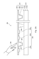
FIG. 2A is the structure diagram of the touch display device according to one embodiment of the present invention. Thetouch display device 201 executes the actions in accordance with the user's touch. For example, if the user'sfinger 200 or a pen presses the icon representing the social group website on thetouch display device 201, the social group website application program is executed. Then the user can link the social group website to check his/her friend's state and other information therein. - The
touch display device 201 includes atouch panel 215 and adisplay device 213. Thetouch panel 215 includes afirst substrate 203, acolor filter layer 219,several photo spacers 207/209, a first transparent electrode layer (Indium Tin oxide; ITO) 205, and a secondtransparent electrode layer 211. - The
color filter layer 219 is disposed on thefirst substrate 203. In general, thecolor filter layer 219 is usually employed to process the light of a single color to produce the colorful images. Thecolor filter layer 219 is mainly composed of thered color filter 219 a, thegreen color filter 219 b, and theblue color filter 219 c. In more detail, the red, the green, and the blue (primary colors) organic materials are formed within each pixel on the glass substrate to produce the color filter (219 a, 219 b, 219 c). Due to the high precision, better light resistance, and better heat endurance, the pigment dispersion method becomes the mainstream to produce the color filters of the current TFT. - The
photo spacer 207/209 are disposed on thefirst substrate 203; the firsttransparent electrode layer 205 covers thecolor filter layer 219 and some of thephoto spacer 207, in which thephoto spacer 207 covered by the firsttransparent electrode layer 205 form the touch sensors. Thephoto spacer 209 is taken for separating the firsttransparent electrode layer 205 and the secondtransparent electrode layer 211, such that the twotransparent electrode layers 205/211 do not contact each other and perform error action unconsciously. The secondtransparent electrode layer 211 is disposed corresponding to the firsttransparent electrode layer 205 and is disposed on a surface of thedisplay device 213 toward thetouch panel 215, in which a voltage variation signal identifying a touched location is generated when thetouch panel 215 is touched to make the firsttransparent electrode layer 205 sink to contact with the secondtransparent electrode layer 211. Then, the analogdigital controller 109 receives the voltage variation signal and converts the voltage variation signal into a digital signal, and theprocessor 111 computes the location to perform the touching function according to the digital signal, as illustrated inFIG. 1 . - Through the
color filter layer 219, thephoto spacer 207, the firsttransparent electrode layer 205, and the secondtransparent electrode layer 211, the touched location is computed and the touching function is performed, and the additional touch panel is no longer required, which reduces the manufacture costs. - The
display device 213, such as an electrophoresis display device, is disposed adjacent to the secondtransparent electrode layer 211 of thetouch panel 215 for display the images, in which thedisplay device 213 is closely contacted with thetouch panel 215. Thedisplay device 213 substantially includes thetransistor array substrate 213 b and theelectrophoresis display layer 213 a. Thetransistor array substrate 213 b has a lot of transistors disposed thereon (not shown), in which thetransistor array substrate 213 b can be a rigid substrate or a flexible substrate. - The
electrophoresis display layer 213 a is disposed on thetransistor array substrate 213 b and also disposed between thetransistor array substrate 213 b and the secondtransparent electrode layer 211, in which theelectrophoresis display layer 213 a can be a microcapsule type electrophoresis display layer controlled by the transistors on thetransistor array substrate 213 b to show the images. In more detail, theelectrophoretic display layer 213 a includes a lot of microcapsules, each microcapsule contains several first charged particles and several second charged particles. - The first charged particles and second charged particles have different colors and different electrical properties; that is, the first charged particles and the second charged particles respectively carry the positive charges and the negative charges. When the transistors of the
transistor arrays substrate 213 b vary the electric field, the first charged particles and the second charged particles are moved, so that thedisplay device 213 can display various pictures. -
FIG. 2B is the structure diagram of the touch display device according to another embodiment of the present invention. Thetouch display device 221 executes the actions in accordance with a user's touch, in which thetouch display device 221 substantially includes atouch panel 225 and adisplay device 213. In this embodiment, thetouch panel 225 and thedisplay device 213 have almost the same structures as shown inFIG. 2A , except that an additional insulatinglayer 223 is contained, and the disposing of the firsttransparent electrode layer 205 inFIG. 2B is slightly different form that shown inFIG. 2A . - In this embodiment, the
color filter layer 219 is disposed on thefirst substrate 203. The insulatinglayer 223 is disposed between thefirst substrate 203 and the firsttransparent electrode layer 205, in which the insulatinglayer 223 covers thecolor filter layer 219 while thephoto spacers 207 and the firsttransparent electrode layer 203 are disposed on the insulatinglayer 223. Thephoto spacer 209 contacts with the firsttransparent electrode layer 205, and thephoto spacer 207 wrapped by the firsttransparent electrode layer 205 forms the touch sensors. When thetouch panel 225 is touched to make the firsttransparent electrode layer 205 sink to contact with the secondtransparent electrode layer 211, a voltage variation signal identifying a touched location is generated. As a result, the touched location/position of thetouch panel 225 can be identified, and the touch function can be implemented without the extra touch panel. - The touch panel and the touch display device of the above embodiments utilize the transparent electrode layer and the gap material (photo spacers) already existing in the display device, in which the transparent electrode layer is attached to the bellowing of the gap material to realize the built-in resistive touch feature. In the meanwhile, the existing color filter layer process can be still used, so the outside touch panel is no longer required, which reduces the manufacturing costs and simplifies the making process.
- It will be apparent to those skilled in the art that various modifications and variations can be made to the structure of the present invention without departing from the scope or spirit of the invention. In view of the foregoing, it is intended that the present invention cover modifications and variations of this invention provided they fall within the scope of the following claims and their equivalents.
Claims (11)
1. A touch panel, comprising:
a first substrate;
a color filter layer disposed on the first substrate;
a plurality of spacers disposed on the first substrate;
a first transparent electrode layer covering the color filter layer and some of the spacers, wherein the spacers covered by the first transparent electrode layer form a plurality of touch sensors; and
a second transparent electrode layer disposed corresponding to the first transparent electrode layer, wherein a voltage variation signal identifying a touched location is generated when the touch panel is touched to make the first transparent electrode layer sink to contact with the second transparent electrode layer.
2. The touch panel as claimed in claim 1 , further comprising:
an insulating layer disposed between the first substrate and the first transparent electrode layer, wherein the insulating layer covers the color filter layer while the spacers and the first transparent electrode layer are disposed on the insulating layer.
3. A touch display device, comprising:
a touch panel comprising:
a first substrate;
a color filter layer disposed on the first substrate;
a plurality of spacers disposed on the first substrate;
a first transparent electrode layer covering the color filter layer and some of the spacers, wherein the spacers covered by the first transparent electrode layer form a plurality of touch sensors; and
a second transparent electrode layer disposed corresponding to the first transparent electrode layer, wherein a voltage variation signal identifying a touched location is generated when the touch panel is touched to make the first transparent electrode layer sink to contact with the second transparent electrode layer; and
a display device, disposed adjacent to the second transparent electrode layer of the touch panel for displaying images.
4. The touch display device as claimed in claim 3 , wherein the second transparent electrode layer is disposed on a surface of the display device toward the touch panel.
5. The touch display device as claimed in claim 3 , wherein the display device is an electrophoresis display device.
6. The touch display device as claimed in claim 5 , wherein the display device comprises:
a transistor array substrate having a plurality of transistors disposed thereon; and
an electrophoresis display layer disposed on the transistor array substrate and between the transistor array substrate and the second transparent electrode layer, wherein the electrophoresis display layer is controlled by the transistors to show images.
7. The touch display device as claimed in claim 6 , wherein the first substrate and the transistor array substrate are rigid substrates or flexible substrates.
8. The touch display device as claimed in claim 6 , wherein the electrophoresis display layer is a microcapsule type electrophoresis display layer.
9. The touch display device as claimed in claim 3 , wherein the touch panel further comprises an insulating layer disposed between the first substrate and the first transparent electrode layer, and the insulating layer covers the color filter layer while the spacers and the first transparent electrode layer are disposed on the insulating layer.
10. The touch display device as claimed in claim 3 , further comprising an analog digital controller for receiving the voltage variation signal and converting the voltage variation signal into a digital signal.
11. The touch display device as claimed in claim 10 , further comprising a processor for computing the touched location according to the digital signal.
Applications Claiming Priority (2)
| Application Number | Priority Date | Filing Date | Title |
|---|---|---|---|
| TW100110800A TWI595403B (en) | 2011-03-29 | 2011-03-29 | Color touch panel, touchable color electrophoresis display panel, and device thereof |
| TW100110800 | 2011-03-29 |
Publications (1)
| Publication Number | Publication Date |
|---|---|
| US20120249447A1 true US20120249447A1 (en) | 2012-10-04 |
Family
ID=46926532
Family Applications (1)
| Application Number | Title | Priority Date | Filing Date |
|---|---|---|---|
| US13/353,987 Abandoned US20120249447A1 (en) | 2011-03-29 | 2012-01-19 | Touch panel and touch display device using the same |
Country Status (3)
| Country | Link |
|---|---|
| US (1) | US20120249447A1 (en) |
| CN (1) | CN102736344B (en) |
| TW (1) | TWI595403B (en) |
Cited By (1)
| Publication number | Priority date | Publication date | Assignee | Title |
|---|---|---|---|---|
| JP2016018011A (en) * | 2014-07-04 | 2016-02-01 | 株式会社ジャパンディスプレイ | Display device |
Families Citing this family (5)
| Publication number | Priority date | Publication date | Assignee | Title |
|---|---|---|---|---|
| EP2735950B1 (en) | 2012-11-22 | 2019-04-03 | LG Innotek Co., Ltd. | Touch window |
| TWI493410B (en) * | 2013-10-08 | 2015-07-21 | E Ink Holdings Inc | Touch display device |
| TWI544465B (en) * | 2014-03-13 | 2016-08-01 | 元太科技工業股份有限公司 | Electrophoretic display apparatus and driving method thereof |
| CN106842665A (en) * | 2017-02-27 | 2017-06-13 | 联想(北京)有限公司 | Liquid crystal display module and electronic equipment |
| CN109283767A (en) * | 2017-07-19 | 2019-01-29 | 黄永兰 | A kind of electrophoretic display apparatus |
Citations (8)
| Publication number | Priority date | Publication date | Assignee | Title |
|---|---|---|---|---|
| US20070252614A1 (en) * | 2006-02-20 | 2007-11-01 | Samsung Electronics Co., Ltd. | Display device and method of testing sensing unit thereof |
| US20070262967A1 (en) * | 2006-05-10 | 2007-11-15 | Rho Soo Guy | Liquid crystal display with built-in touch screen |
| US20080136980A1 (en) * | 2006-12-08 | 2008-06-12 | Samsung Electronics Co., Ltd. | Liquid crystal display device and method of fabricating the same |
| US20090237369A1 (en) * | 2008-03-19 | 2009-09-24 | Samsung Electronics Co., Ltd. | Touch panel display and method of manufacturing the same |
| US20100295811A1 (en) * | 2007-12-14 | 2010-11-25 | Ulvac, Inc. | Touch panel and method for manufacturing touch panel |
| US20100309151A1 (en) * | 2009-06-04 | 2010-12-09 | Au Optronics Corp. | Touch panel and method for manufacturing the same |
| US20110148668A1 (en) * | 2009-12-17 | 2011-06-23 | Shenzhen Futaihong Precision Industry Co., Ltd. | System and method for protecting a resistive touch panel of a communication device |
| US20110234513A1 (en) * | 2010-03-26 | 2011-09-29 | Hong Fu Jin Precision Industry (Shenzhen) Co., Ltd | Electronic paper display device with touch function |
Family Cites Families (4)
| Publication number | Priority date | Publication date | Assignee | Title |
|---|---|---|---|---|
| KR100835920B1 (en) * | 2001-12-27 | 2008-06-09 | 엘지디스플레이 주식회사 | Liquid Crystal Display Panel Associated With Touch Panel |
| CN101551544B (en) * | 2008-04-03 | 2010-12-08 | 胜华科技股份有限公司 | Colorful filter with touch function and liquid crystal display device |
| CN101266352A (en) * | 2008-05-08 | 2008-09-17 | 友达光电股份有限公司 | Touch control display panel, colorful filtering substrate and its manufacture method |
| CN101988999B (en) * | 2009-07-31 | 2013-11-06 | 胜华科技股份有限公司 | Touch display and touch panel thereof |
-
2011
- 2011-03-29 TW TW100110800A patent/TWI595403B/en active
- 2011-04-26 CN CN201110112554.7A patent/CN102736344B/en active Active
-
2012
- 2012-01-19 US US13/353,987 patent/US20120249447A1/en not_active Abandoned
Patent Citations (8)
| Publication number | Priority date | Publication date | Assignee | Title |
|---|---|---|---|---|
| US20070252614A1 (en) * | 2006-02-20 | 2007-11-01 | Samsung Electronics Co., Ltd. | Display device and method of testing sensing unit thereof |
| US20070262967A1 (en) * | 2006-05-10 | 2007-11-15 | Rho Soo Guy | Liquid crystal display with built-in touch screen |
| US20080136980A1 (en) * | 2006-12-08 | 2008-06-12 | Samsung Electronics Co., Ltd. | Liquid crystal display device and method of fabricating the same |
| US20100295811A1 (en) * | 2007-12-14 | 2010-11-25 | Ulvac, Inc. | Touch panel and method for manufacturing touch panel |
| US20090237369A1 (en) * | 2008-03-19 | 2009-09-24 | Samsung Electronics Co., Ltd. | Touch panel display and method of manufacturing the same |
| US20100309151A1 (en) * | 2009-06-04 | 2010-12-09 | Au Optronics Corp. | Touch panel and method for manufacturing the same |
| US20110148668A1 (en) * | 2009-12-17 | 2011-06-23 | Shenzhen Futaihong Precision Industry Co., Ltd. | System and method for protecting a resistive touch panel of a communication device |
| US20110234513A1 (en) * | 2010-03-26 | 2011-09-29 | Hong Fu Jin Precision Industry (Shenzhen) Co., Ltd | Electronic paper display device with touch function |
Cited By (3)
| Publication number | Priority date | Publication date | Assignee | Title |
|---|---|---|---|---|
| JP2016018011A (en) * | 2014-07-04 | 2016-02-01 | 株式会社ジャパンディスプレイ | Display device |
| US10739917B2 (en) | 2014-07-04 | 2020-08-11 | Japan Display Inc. | Display apparatus with driving electrodes and auxiliary electrodes |
| US11226680B2 (en) | 2014-07-04 | 2022-01-18 | Japan Display Inc. | Display apparatus with shield signal |
Also Published As
| Publication number | Publication date |
|---|---|
| CN102736344B (en) | 2015-04-01 |
| TW201239721A (en) | 2012-10-01 |
| TWI595403B (en) | 2017-08-11 |
| CN102736344A (en) | 2012-10-17 |
Similar Documents
| Publication | Publication Date | Title |
|---|---|---|
| TWI467298B (en) | Liquid crystal display device | |
| US10151947B2 (en) | In-cell touch liquid crystal display device and method of manufacturing the same | |
| US8178383B2 (en) | Touch-sensing display device and method for manufacturing the same | |
| US9582041B2 (en) | Touch-control display and fabrication method thereof | |
| CN100476531C (en) | Touch control type planar display and producing method thereof | |
| WO2016115842A1 (en) | Colour film substrate, array substrate and display device | |
| US9459481B2 (en) | In-cell touch display panel structure | |
| US20120044178A1 (en) | Liquid Crystal Display Device with Built-In Touch Screen | |
| US20120249447A1 (en) | Touch panel and touch display device using the same | |
| KR102231934B1 (en) | DISPLAY DEVICE WITH INTEGRATED TOUCH SCREEN AND Method for Manufacturing | |
| TWI485599B (en) | Touch component and flat panel display | |
| WO2018149125A1 (en) | Touch control substrate, manufacturing method thereof, and touch control display device | |
| CN106406591B (en) | OLED touch base plate, its manufacturing method and control method | |
| JP5515845B2 (en) | Color filter with resistive touch panel function and display device including the color filter | |
| US9046707B2 (en) | Touch-sensing liquid crystal panel and fabrication method thereof | |
| KR20080072395A (en) | Display device | |
| CN105139775A (en) | Embedded touch panel | |
| US10025131B2 (en) | Touch-sensing liquid crystal panel and fabrication method thereof | |
| WO2013125191A1 (en) | Input device | |
| KR101432569B1 (en) | Liquid crystal display device having touch screen and method for fabricating the same | |
| US10571753B2 (en) | Liquid crystal panel | |
| US10216306B2 (en) | Touch panel-equipped display device | |
| US8334848B2 (en) | Resistance type touch display panel | |
| TW201039036A (en) | Touch electrophoretic display | |
| KR20120065157A (en) | Touch panel and a flat panel display device comprising the same |
Legal Events
| Date | Code | Title | Description |
|---|---|---|---|
| AS | Assignment |
Owner name: E INK HOLDINGS INC., TAIWAN Free format text: ASSIGNMENT OF ASSIGNORS INTEREST;ASSIGNOR:TSAI, WEI-CHEN;REEL/FRAME:027562/0651 Effective date: 20110722 |
|
| STCB | Information on status: application discontinuation |
Free format text: ABANDONED -- FAILURE TO RESPOND TO AN OFFICE ACTION |