US20120249281A1 - Inductor and eddy current sensor including an inductor - Google Patents
Inductor and eddy current sensor including an inductor Download PDFInfo
- Publication number
- US20120249281A1 US20120249281A1 US13/079,404 US201113079404A US2012249281A1 US 20120249281 A1 US20120249281 A1 US 20120249281A1 US 201113079404 A US201113079404 A US 201113079404A US 2012249281 A1 US2012249281 A1 US 2012249281A1
- Authority
- US
- United States
- Prior art keywords
- inductor
- metal layer
- patterned metal
- insulating substrate
- eddy current
- Prior art date
- Legal status (The legal status is an assumption and is not a legal conclusion. Google has not performed a legal analysis and makes no representation as to the accuracy of the status listed.)
- Abandoned
Links
- 229910052751 metal Inorganic materials 0.000 claims abstract description 78
- 239000002184 metal Substances 0.000 claims abstract description 78
- 239000000758 substrate Substances 0.000 claims abstract description 46
- 239000004020 conductor Substances 0.000 claims description 16
- BASFCYQUMIYNBI-UHFFFAOYSA-N platinum Chemical compound [Pt] BASFCYQUMIYNBI-UHFFFAOYSA-N 0.000 claims description 16
- 229910045601 alloy Inorganic materials 0.000 claims description 10
- 239000000956 alloy Substances 0.000 claims description 10
- PXHVJJICTQNCMI-UHFFFAOYSA-N Nickel Chemical compound [Ni] PXHVJJICTQNCMI-UHFFFAOYSA-N 0.000 claims description 8
- 229910052697 platinum Inorganic materials 0.000 claims description 8
- PNEYBMLMFCGWSK-UHFFFAOYSA-N aluminium oxide Inorganic materials [O-2].[O-2].[O-2].[Al+3].[Al+3] PNEYBMLMFCGWSK-UHFFFAOYSA-N 0.000 claims description 5
- ZOKXTWBITQBERF-UHFFFAOYSA-N Molybdenum Chemical compound [Mo] ZOKXTWBITQBERF-UHFFFAOYSA-N 0.000 claims description 4
- RTAQQCXQSZGOHL-UHFFFAOYSA-N Titanium Chemical compound [Ti] RTAQQCXQSZGOHL-UHFFFAOYSA-N 0.000 claims description 4
- PCHJSUWPFVWCPO-UHFFFAOYSA-N gold Chemical compound [Au] PCHJSUWPFVWCPO-UHFFFAOYSA-N 0.000 claims description 4
- 239000010931 gold Substances 0.000 claims description 4
- 229910052737 gold Inorganic materials 0.000 claims description 4
- 229910052750 molybdenum Inorganic materials 0.000 claims description 4
- 239000011733 molybdenum Substances 0.000 claims description 4
- 229910052759 nickel Inorganic materials 0.000 claims description 4
- 239000010936 titanium Substances 0.000 claims description 4
- 229910052719 titanium Inorganic materials 0.000 claims description 4
- WFKWXMTUELFFGS-UHFFFAOYSA-N tungsten Chemical compound [W] WFKWXMTUELFFGS-UHFFFAOYSA-N 0.000 claims description 4
- 229910052721 tungsten Inorganic materials 0.000 claims description 4
- 239000010937 tungsten Substances 0.000 claims description 4
- 238000007747 plating Methods 0.000 claims description 3
- PMHQVHHXPFUNSP-UHFFFAOYSA-M copper(1+);methylsulfanylmethane;bromide Chemical compound Br[Cu].CSC PMHQVHHXPFUNSP-UHFFFAOYSA-M 0.000 claims description 2
- 229910052594 sapphire Inorganic materials 0.000 claims description 2
- 239000010980 sapphire Substances 0.000 claims description 2
- 238000000034 method Methods 0.000 description 14
- 239000000463 material Substances 0.000 description 8
- 238000005259 measurement Methods 0.000 description 7
- 238000013508 migration Methods 0.000 description 5
- 230000005012 migration Effects 0.000 description 5
- 238000005530 etching Methods 0.000 description 4
- 238000007650 screen-printing Methods 0.000 description 4
- 238000002485 combustion reaction Methods 0.000 description 3
- 230000001939 inductive effect Effects 0.000 description 3
- 238000012216 screening Methods 0.000 description 3
- VYZAMTAEIAYCRO-UHFFFAOYSA-N Chromium Chemical compound [Cr] VYZAMTAEIAYCRO-UHFFFAOYSA-N 0.000 description 2
- RYGMFSIKBFXOCR-UHFFFAOYSA-N Copper Chemical compound [Cu] RYGMFSIKBFXOCR-UHFFFAOYSA-N 0.000 description 2
- BQCADISMDOOEFD-UHFFFAOYSA-N Silver Chemical compound [Ag] BQCADISMDOOEFD-UHFFFAOYSA-N 0.000 description 2
- MCMNRKCIXSYSNV-UHFFFAOYSA-N Zirconium dioxide Chemical compound O=[Zr]=O MCMNRKCIXSYSNV-UHFFFAOYSA-N 0.000 description 2
- 229910052782 aluminium Inorganic materials 0.000 description 2
- XAGFODPZIPBFFR-UHFFFAOYSA-N aluminium Chemical compound [Al] XAGFODPZIPBFFR-UHFFFAOYSA-N 0.000 description 2
- 238000005219 brazing Methods 0.000 description 2
- 239000000919 ceramic Substances 0.000 description 2
- 229910052804 chromium Inorganic materials 0.000 description 2
- 239000011651 chromium Substances 0.000 description 2
- 229910052802 copper Inorganic materials 0.000 description 2
- 239000010949 copper Substances 0.000 description 2
- 230000032798 delamination Effects 0.000 description 2
- 238000000151 deposition Methods 0.000 description 2
- 230000000694 effects Effects 0.000 description 2
- 238000009713 electroplating Methods 0.000 description 2
- 238000010304 firing Methods 0.000 description 2
- 238000009659 non-destructive testing Methods 0.000 description 2
- 229910052709 silver Inorganic materials 0.000 description 2
- 239000004332 silver Substances 0.000 description 2
- 229910052715 tantalum Inorganic materials 0.000 description 2
- GUVRBAGPIYLISA-UHFFFAOYSA-N tantalum atom Chemical compound [Ta] GUVRBAGPIYLISA-UHFFFAOYSA-N 0.000 description 2
- 235000001674 Agaricus brunnescens Nutrition 0.000 description 1
- 229910001020 Au alloy Inorganic materials 0.000 description 1
- 229910052581 Si3N4 Inorganic materials 0.000 description 1
- 239000000654 additive Substances 0.000 description 1
- 239000005388 borosilicate glass Substances 0.000 description 1
- 230000002596 correlated effect Effects 0.000 description 1
- 230000003247 decreasing effect Effects 0.000 description 1
- 210000003298 dental enamel Anatomy 0.000 description 1
- 239000012777 electrically insulating material Substances 0.000 description 1
- 238000001704 evaporation Methods 0.000 description 1
- 230000008020 evaporation Effects 0.000 description 1
- 239000003353 gold alloy Substances 0.000 description 1
- 238000010438 heat treatment Methods 0.000 description 1
- 239000012535 impurity Substances 0.000 description 1
- 230000006698 induction Effects 0.000 description 1
- 238000007689 inspection Methods 0.000 description 1
- 239000011810 insulating material Substances 0.000 description 1
- 238000002955 isolation Methods 0.000 description 1
- 239000007769 metal material Substances 0.000 description 1
- 239000000203 mixture Substances 0.000 description 1
- 238000012986 modification Methods 0.000 description 1
- 230000004048 modification Effects 0.000 description 1
- 238000012545 processing Methods 0.000 description 1
- 230000000750 progressive effect Effects 0.000 description 1
- 239000010453 quartz Substances 0.000 description 1
- 238000005070 sampling Methods 0.000 description 1
- HBMJWWWQQXIZIP-UHFFFAOYSA-N silicon carbide Chemical compound [Si+]#[C-] HBMJWWWQQXIZIP-UHFFFAOYSA-N 0.000 description 1
- 229910010271 silicon carbide Inorganic materials 0.000 description 1
- VYPSYNLAJGMNEJ-UHFFFAOYSA-N silicon dioxide Inorganic materials O=[Si]=O VYPSYNLAJGMNEJ-UHFFFAOYSA-N 0.000 description 1
- HQVNEWCFYHHQES-UHFFFAOYSA-N silicon nitride Chemical compound N12[Si]34N5[Si]62N3[Si]51N64 HQVNEWCFYHHQES-UHFFFAOYSA-N 0.000 description 1
- 238000005245 sintering Methods 0.000 description 1
- 238000004544 sputter deposition Methods 0.000 description 1
- 239000010938 white gold Substances 0.000 description 1
- 229910000832 white gold Inorganic materials 0.000 description 1
- 229910000859 α-Fe Inorganic materials 0.000 description 1
Images


Classifications
-
- H—ELECTRICITY
- H01—ELECTRIC ELEMENTS
- H01F—MAGNETS; INDUCTANCES; TRANSFORMERS; SELECTION OF MATERIALS FOR THEIR MAGNETIC PROPERTIES
- H01F17/00—Fixed inductances of the signal type
- H01F17/0006—Printed inductances
- H01F17/0013—Printed inductances with stacked layers
-
- G—PHYSICS
- G01—MEASURING; TESTING
- G01N—INVESTIGATING OR ANALYSING MATERIALS BY DETERMINING THEIR CHEMICAL OR PHYSICAL PROPERTIES
- G01N27/00—Investigating or analysing materials by the use of electric, electrochemical, or magnetic means
- G01N27/72—Investigating or analysing materials by the use of electric, electrochemical, or magnetic means by investigating magnetic variables
- G01N27/82—Investigating or analysing materials by the use of electric, electrochemical, or magnetic means by investigating magnetic variables for investigating the presence of flaws
- G01N27/90—Investigating or analysing materials by the use of electric, electrochemical, or magnetic means by investigating magnetic variables for investigating the presence of flaws using eddy currents
- G01N27/9006—Details, e.g. in the structure or functioning of sensors
-
- H—ELECTRICITY
- H01—ELECTRIC ELEMENTS
- H01F—MAGNETS; INDUCTANCES; TRANSFORMERS; SELECTION OF MATERIALS FOR THEIR MAGNETIC PROPERTIES
- H01F17/00—Fixed inductances of the signal type
- H01F17/0006—Printed inductances
- H01F2017/0046—Printed inductances with a conductive path having a bridge
Definitions
- the present invention is directed to inductors and articles and systems including inductors, more particularly, inductors capable of measuring eddy currents.
- Eddy current are currents induced in conductors that are generated by a changing magnetic field. Relative motion of the magnetic field and the conductor causes a circulating flow of current known as eddies. These eddies create induced magnetic fields that oppose the changing magnetic field.
- the induced magnetic fields can be used for measuring vibration, position sensing, metal separating, induction heating, non-destructive testing of conductive materials, or other applications.
- Known eddy current sensors include inductors for measuring eddy current.
- the eddy current sensors include a coiled wire, such as enamel coated wire, wrapped around a bobbin, such as a ferrite bobbin.
- a coiled wire such as enamel coated wire
- Such eddy current sensors suffer from several drawbacks.
- the wrapping of the wire around the bobbin can be inconsistent from one inductor to another.
- Such inconsistencies can require complicated procedures for utilizing the inductor in an eddy current sensor.
- the wire can unravel from the bobbin and/or tension in the wire can result in undesirable tensile effects on the wire.
- many eddy current sensors are only operable between about ⁇ 25° C. ( ⁇ 13° F.) and about 175° C. (347° F.) and some are operable only within narrower ranges.
- an inductor includes a patterned metal layer arranged on an insulating substrate.
- the inductor is capable of sensing eddy current of a region, the region being at a temperature up to about 500° C. (932° F.).
- an inductor in another exemplary embodiment, includes a patterned metal layer on an insulating substrate and a conductive material on the patterned metal layer.
- the inductor is capable of sensing eddy current of a region, the region being at a temperature up to about 500° C. (932° F.).
- an eddy current sensor in another exemplary embodiment, includes a transducer having an inductor.
- the inductor includes a patterned metal layer arranged on an insulating substrate.
- the inductor is capable of sensing eddy current of a region, the region being at a temperature up to about 500° C. (932° F.).
- FIG. 1 shows a perspective view from above of an exemplary inductor according to the disclosure.
- FIG. 2 shows a perspective view from below of an exemplary inductor according to the disclosure.
- FIG. 3 shows a perspective view of an exemplary inductor according to the disclosure.
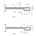
- FIG. 4 shows a sectional view of an exemplary eddy current sensor according to the disclosure.
- FIG. 5 shows a sectional view of an exemplary eddy current sensor according to the disclosure.
- an inductor and an eddy current sensor including an inductor that do not suffer from one or more of the above drawbacks.
- Embodiments of the disclosure permit measurement of vibration, position sensing, metal separating, non-destructive testing of conductive materials, consistency from one inductor to another, simplified procedures for utilizing the inductor in an eddy current sensor, operation in high temperatures, and combinations thereof.
- FIGS. 1 and 2 show an exemplary embodiment of an inductor 100 .
- the inductor 100 includes a patterned metal layer 102 arranged on a first surface 104 of an insulating substrate 106 .
- the patterned metal layer 102 is any suitable pattern. Suitable patterns include, but are not limited to, spirals, rectilinear spiral-like paths, and other geometric arrangements capable of providing an inductive effect.
- the pattern includes a predetermined number of turns.
- the term “turn” refers to a path extending along 360 degrees from a central reference point. For example, in a spiral pattern, the turns extend in a substantially spiraling manner around the central reference point.
- the turns extend in a substantially spiraling rectilinear manner around the central reference point.
- the pattern includes 16 turns on one layer.
- the pattern includes 32 turns on two layers, with 16 turns on each layer.
- more than 16 turns are included on one layer and/or more than 32 turns are included in the overall pattern for the inductor 100 .
- the patterned metal layer 102 includes a predetermined trace width 103 (the thickness taken in a radial direction along the path of the pattern), a predetermined trace spacing 105 (the spacing between portions taken in a radial direction along the path of the pattern), and a predetermined depth 107 (the distance from the insulating substrate 106 to applied patterned metal layer 102 ).
- the predetermined trace width 103 is between about 240 micrometers (about 0.00944 inches) and about 267 micrometers (about 0.0105 inches) or at about 254 micrometers (0.010 inches).
- the predetermined trace spacing 105 is between about 216 micrometers (about 0.00850 inches) and about 190 micrometers (about 0.00748 inches) or at about 203 micrometers (about 0.00799 inches).
- the predetermined depth 107 is between about 19 micrometers (about 0.000748 inches) and about 35 micrometers (0.00138 inches), between about 19 micrometers (about 0.000748 inches) and about 26 micrometers (about 0.00102 inches) on the interior of the spiral-shaped pattern, between about 29 micrometers (about 0.00114 inches) and about 35 micrometers (about 0.001378 inches) on the exterior of the spiral-shaped pattern, about 22 micrometers (about 0.000866 inches) on the interior of the spiral-shaped pattern, and about 31 micrometers (about 0.00122 inches) on the exterior of the spiral-shaped pattern.
- the patterned metal layer 102 is not limited to metal materials and includes any suitable inductive materials. Suitable materials for the patterned metal layer 102 include, but are not limited to, platinum, molybdenum, tungsten, tantalum, nickel, titanium, copper, chromium, gold, aluminum, silver or other conductive materials appropriate for the operating temperature. In one embodiment, the patterned metal layer 102 includes a seed layer of platinum thick film, for example, about 10 micrometers (about 0.000393 inches), and a plating of 99.9% platinum, for example, about 25 micrometers (about 0.000984 inches). The seed layer provides adhesion by migration into the insulating substrate 106 . The plating provides consistency by having substantially consistent depth throughout the patterned metal layer 102 . In one embodiment, the patterned metal layer 102 includes additives for adhesion and/or impurities, which may or may not be metal. For example, the patterned metal layer 102 may include ceramics, such as alumina.
- the platinum seed layer provides adhesion and peel strength.
- low enough resistance and consequently a desirable performing inductive effect and/or eddy current effects are achieved by using electroplated platinum, for example, at an average about 25.4 micrometers (about 0.001 inches), and/or multiple silk screening passes to construct a thicker conductor thereby decreasing resistance. Electroplating permits control of the turn-to-turn spacing as the build-up causes the conductor cross-section to “mushroom” thus reducing the predetermined trace spacing 105 .
- the electroplating includes the predetermined trace spacing 105 (and consequently total inductance) and a predetermined build-up height (and total resistance).
- Multiple passes of silk screening include each layer being fired or cured and each additional layer being deposited until a predetermined average thickness, for example, a 25.4 micrometers (about 0.001 inch) thickness or a thickness of at least 25.4 micrometers (about 0.001 inches), is constructed.
- Silk screening registration includes each progressive pass being thinner (in a radial direction) than the prior pass.
- the insulating substrate 106 is any suitable electrically insulating material. Suitable materials for the insulating substrate 106 include, but are not limited to, alumina (for example, 92% alumina), aluminum nitride, borosilicate glass, quartz, sialon, low-temperature co-fired ceramic, silicon nitride, alumina, silicon carbide, sapphire, zirconia, or other suitable insulating materials. In one embodiment, the insulating substrate 106 has a predetermined geometry and dimensions, for example, a substantially square geometry having dimensions of about 2.5 cm (about 0.98 inches) to about 2.6 cm (about 1.0 inches) or about 2.55 cm (about 1.00 inches) or any other suitable geometry and dimensions capable of supporting the patterned metal layer 102 .
- the insulating substrate 106 has a predetermined thickness, for example, about 1,550 micrometers (about 0.06102 inches) to about 1,800 micrometers (about 0.07087 inches) or about 1,675 micrometers (about 0.06594 inches. In one embodiment, the insulating substrate 106 has a predetermined flatness, for example, about 75 micrometers (about 0.0030 inches).
- a via 202 extends through the insulating substrate 106 from the patterned metal layer 102 onto a second surface 204 .
- the via 202 includes any suitable conductive materials. Suitable materials for the via 202 include, but are not limited to, platinum, molybdenum, tungsten, tantalum, nickel, titanium, copper, chromium, gold, aluminum, silver, or other suitable conductive materials.
- the via 202 and the patterned metal layer 102 include the same material.
- the via 202 has a predetermined diameter, for example, about 230 micrometers (about 0.00906 inches) to about 280 micrometers (about 0.0110 inches) or about 255 micrometers (about 0.0100 inches).
- the patterned metal layer 102 is operably connected to a first conductive pad 108 on the first surface 104 and the via 202 is operably connected to a second conductive pad 110 on the second surface 204 .
- the first conductive pad 108 and/or second conductive pad 110 include any suitable nickel-based alloy, titanium-based alloy, tungsten-based alloy, gold-based alloy, molybdenum-based alloy, or other conductive metal.
- the inductor 100 is capable of sensing changes in eddy current that, in turn, permit measurement by an eddy current sensor 400 (discussed below with reference to FIG. 4 ) in any suitable high-temperature region, for example, including, but not limited to, a gas turbine component, a steam turbine component, a combustion region, a high-temperature region, a hot manufactured product, or any other region.
- the inductor 100 includes predetermined electrical properties permitting measurement of the eddy current. For example, in one embodiment, at about 25° C. (about 77° F.) the inductor 100 includes inductance at 2 Mhz greater than 1.4 microHenries, greater than 1 Q, Rdc greater than 1, resistance at 2 Mhz greater than 100, max Ipk of 15 mA, isolation greater than 10M, and combinations thereof. In one embodiment, the inductor 100 accurately and/or precisely senses eddy current changes throughout a predetermined temperature or temperature range, for example, up to about 500° C. (about 932° F.), up to about 800° C. (about 1472° F.), up to about 980° C. (about 1796° F.), up to about 1000° C.
- the inductor 100 accurately and/or precisely senses eddy current changes at a predetermined humidity.
- FIG. 3 shows a perspective view of another exemplary embodiment of the inductor 100 .
- the inductor 100 includes the patterned metal layer 102 arranged on the first surface 104 of the insulating substrate 106 .
- the inductor 100 includes a second patterned metal layer 302 arranged on a second insulating substrate 306 .
- the second metal layer 302 is arranged on the first surface 104 or the second surface 204 of the second insulating substrate 306 .
- the second metal layer 302 is arranged on the second surface 204 and a third patterned metal layer (not shown) is arranged on the first surface 104 of the second insulating substrate 306 .
- a third patterned metal layer (not shown) is arranged on a third insulating substrate (not shown).
- two, three, four, or more insulating substrates each having one or two metal layers are arranged on one or both surfaces of each insulating substrate providing any suitable number of turns within the inductor 100 .
- the second patterned metal layer 302 is operably connected to the first patterned metal layer 102 .
- the second patterned metal layer 302 is connected to the first patterned metal layer 102 through a plurality of vias 304 generally extending from the first insulating substrate 106 to the second insulating substrate 306 .
- the plurality of vias 304 includes three vias with the first patterned metal layer 102 and the second patterned metal layer 302 overlapping each via of the plurality of vias 304 .
- the plurality of vias 304 reduce or eliminate resistance caused by joining the first patterned metal layer 102 and the second patterned metal layer 302 .
- the second patterned metal layer 302 includes any suitable features and/or properties described above with reference to the first patterned metal layer 102 .
- the plurality of vias 304 include any suitable features and/or properties described above with reference to the via 202 .
- the second insulating substrate 306 includes any suitable features and/or properties described above with reference to the first insulating substrate 106 .
- the first patterned metal layer 102 is operably connected to the first conductive pad 108 at one end of the pattern and the plurality of vias 304 at the other end of the pattern.
- the second patterned metal layer 302 is operably connected to the plurality of vias 304 at one end of the pattern and the second conductive pad 110 at the other end of the pattern, either directly or through an additional via.
- the inductor 100 is capable of sensing changes in eddy current that, in turn, permit measurement by the eddy current sensor 400 (see FIG. 4 ).
- the inductor 100 is fabricated by a direct-write process, a screen-printing process, an etching process, sputtering, evaporation, sintering, or combinations thereof.
- the direct-write process is used to form the first patterned metal layer 102 on the insulating substrate 106 , for example, as shown in FIG. 1 .
- the first conductive pad 108 and the second conductive pad 110 are written on the insulating substrate 106 and configured for external electrical connection, for example, by gold alloy brazing or white gold brazing.
- the first patterned metal layer 102 , first conductive pad 108 , and the second conductive pad 110 are fired at an elevated temperature, such as 1300° C.
- an additional step of depositing additional conductive material of the first patterned metal layer 102 and/or the second patterned metal layer 302 reduces resistance caused by the migration of the first patterned metal layer 102 and/or the second patterned metal layer into the insulating substrate 302 , provides inductance consistency between portions of the inductor 100 , and provides consistency between inductors 100 made through the direct-write process.
- the screen-printing process or the etching process is used to form the first patterned metal layer 102 on the first insulating substrate 106 and/or the second patterned metal layer 302 on the second insulating substrate 306 , for example, as shown in FIG. 3 .
- the first patterned metal layer 102 and the plurality of vias 304 are formed on the first insulating substrate 106 and the second patterned metal layer 302 and the plurality of vias 304 are formed on the second insulating substrate 306 .
- the first patterned metal layer 102 , the second patterned metal layer 306 and the plurality of vias 304 are then fired at an elevated temperature, such as 1300° C.
- This elevated-temperature firing creates high mechanical peel strength, for example, being resistant to flaking or delamination under repeated cycles, based upon migration of the first pattern metal layer 102 into the first insulating substrate 106 and/or the second patterned metal layer 302 into the second insulating substrate 306 .
- an additional step of depositing additional conductive material of the first patterned metal layer 102 and/or the second patterned metal layer 302 reduces resistance caused by the migration of the first patterned metal layer 102 into the first insulating substrate 106 and/or the second patterned metal layer 302 into the second insulating substrate 304 , provides consistency between portions of the inductor 100 , and provides consistency between inductors 100 made through the screen-printing process or the etching process.
- the eddy current sensor 400 is capable of measurement of current between the first conductive pad 108 and the second conductive pad 110 based upon changes in eddy current sensed by the inductor 100 .
- the eddy current sensor 400 is capable of operation in any suitable region, for example, including, but not limited to, a gas turbine component, a steam turbine component, a combustion region, a high-temperature region, a hot manufactured product, or any other region.
- the region is at a predetermined temperature, for example, up to about 500° C. (about 932° F.), up to about 800° C. (about 1472° F.), up to about 980° C. (about 1796° F.), up to about 1000° C.
- the region includes a predetermined humidity.
- the eddy current sensor 400 includes a transducer 401 having a first electrical lead 402 , a first conductor 404 , and a first cable 406 operatively coupled to the first conductive pad 108 of the inductor 100 and a second electrical lead 402 , a second conductor 404 , and a second cable 406 operatively coupled to the second conductive pad 110 of the inductor 100 .
- the transducer 401 is coupled to a machine (not shown) for sensing dynamic data that may be correlated to a property measurable through eddy current, for example, a gap distance defined between the inductor 100 and a conductive or metallic target, such as, but not limited to, a rotating shaft of the machine, a gas turbine component, a steam turbine component, a combustion region, a high-temperature region, a hot manufactured product, or a component being monitored for material composition and/or material integrity.
- a machine not shown
- a machine for sensing dynamic data that may be correlated to a property measurable through eddy current, for example, a gap distance defined between the inductor 100 and a conductive or metallic target, such as, but not limited to, a rotating shaft of the machine, a gas turbine component, a steam turbine component, a combustion region, a high-temperature region, a hot manufactured product, or a component being monitored for material composition and/or material integrity.
- the eddy current sensor 400 includes any other suitable components.
- the eddy current sensor 400 includes one or more resistors, filters, signal generators, timing control circuits, sampling circuits, convolution circuits, digital signal processors, microprocessors (for example, central processing units, application specific integrated circuits, logic circuits, or any other circuit or processor capable of executing an inspection system), other suitable components, or combinations thereof.
Landscapes
- Chemical & Material Sciences (AREA)
- Power Engineering (AREA)
- Engineering & Computer Science (AREA)
- Health & Medical Sciences (AREA)
- Immunology (AREA)
- Life Sciences & Earth Sciences (AREA)
- Analytical Chemistry (AREA)
- Biochemistry (AREA)
- General Health & Medical Sciences (AREA)
- General Physics & Mathematics (AREA)
- Physics & Mathematics (AREA)
- Pathology (AREA)
- Electrochemistry (AREA)
- Microelectronics & Electronic Packaging (AREA)
- Chemical Kinetics & Catalysis (AREA)
- Coils Or Transformers For Communication (AREA)
- Manufacturing Cores, Coils, And Magnets (AREA)
- Investigating Or Analyzing Materials By The Use Of Magnetic Means (AREA)
- Transmission And Conversion Of Sensor Element Output (AREA)
Abstract
An inductor and an eddy current sensor including an inductor are disclosed. The inductor includes a patterned metal layer arranged on an insulating substrate. The inductor is capable of sensing eddy current within a high temperature region.
Description
- The present invention is directed to inductors and articles and systems including inductors, more particularly, inductors capable of measuring eddy currents.
- Eddy current are currents induced in conductors that are generated by a changing magnetic field. Relative motion of the magnetic field and the conductor causes a circulating flow of current known as eddies. These eddies create induced magnetic fields that oppose the changing magnetic field. The induced magnetic fields can be used for measuring vibration, position sensing, metal separating, induction heating, non-destructive testing of conductive materials, or other applications.
- Known eddy current sensors include inductors for measuring eddy current. Generally, the eddy current sensors include a coiled wire, such as enamel coated wire, wrapped around a bobbin, such as a ferrite bobbin. Such eddy current sensors suffer from several drawbacks. For example, the wrapping of the wire around the bobbin can be inconsistent from one inductor to another. Such inconsistencies can require complicated procedures for utilizing the inductor in an eddy current sensor. Also, in high temperature environments, the wire can unravel from the bobbin and/or tension in the wire can result in undesirable tensile effects on the wire. As such, many eddy current sensors are only operable between about −25° C. (−13° F.) and about 175° C. (347° F.) and some are operable only within narrower ranges.
- An inductor and an eddy current sensor including an inductor that do not suffer from the above drawbacks would be desirable in the art.
- In an exemplary embodiment, an inductor includes a patterned metal layer arranged on an insulating substrate. The inductor is capable of sensing eddy current of a region, the region being at a temperature up to about 500° C. (932° F.).
- In another exemplary embodiment, an inductor includes a patterned metal layer on an insulating substrate and a conductive material on the patterned metal layer. The inductor is capable of sensing eddy current of a region, the region being at a temperature up to about 500° C. (932° F.).
- In another exemplary embodiment, an eddy current sensor includes a transducer having an inductor. The inductor includes a patterned metal layer arranged on an insulating substrate. The inductor is capable of sensing eddy current of a region, the region being at a temperature up to about 500° C. (932° F.).
- Other features and advantages of the present invention will be apparent from the following more detailed description of the preferred embodiment, taken in conjunction with the accompanying drawings which illustrate, by way of example, the principles of the invention.
-
FIG. 1 shows a perspective view from above of an exemplary inductor according to the disclosure. -
FIG. 2 shows a perspective view from below of an exemplary inductor according to the disclosure. -
FIG. 3 shows a perspective view of an exemplary inductor according to the disclosure. -
FIG. 4 shows a sectional view of an exemplary eddy current sensor according to the disclosure. -
FIG. 5 shows a sectional view of an exemplary eddy current sensor according to the disclosure. - Wherever possible, the same reference numbers will be used throughout the drawings to represent the same parts.
- Provided is an inductor and an eddy current sensor including an inductor that do not suffer from one or more of the above drawbacks. Embodiments of the disclosure permit measurement of vibration, position sensing, metal separating, non-destructive testing of conductive materials, consistency from one inductor to another, simplified procedures for utilizing the inductor in an eddy current sensor, operation in high temperatures, and combinations thereof.
-
FIGS. 1 and 2 show an exemplary embodiment of aninductor 100. As shown inFIG. 1 , theinductor 100 includes a patternedmetal layer 102 arranged on afirst surface 104 of aninsulating substrate 106. The patternedmetal layer 102 is any suitable pattern. Suitable patterns include, but are not limited to, spirals, rectilinear spiral-like paths, and other geometric arrangements capable of providing an inductive effect. In one embodiment, the pattern includes a predetermined number of turns. As used herein, the term “turn” refers to a path extending along 360 degrees from a central reference point. For example, in a spiral pattern, the turns extend in a substantially spiraling manner around the central reference point. In a rectilinear spiral-like path, the turns extend in a substantially spiraling rectilinear manner around the central reference point. For example, in one embodiment, the pattern includes 16 turns on one layer. In another embodiment, the pattern includes 32 turns on two layers, with 16 turns on each layer. In other embodiment, more than 16 turns are included on one layer and/or more than 32 turns are included in the overall pattern for theinductor 100. - In one embodiment, as shown in
FIGS. 1 and 4 , the patternedmetal layer 102 includes a predetermined trace width 103 (the thickness taken in a radial direction along the path of the pattern), a predetermined trace spacing 105 (the spacing between portions taken in a radial direction along the path of the pattern), and a predetermined depth 107 (the distance from theinsulating substrate 106 to applied patterned metal layer 102). In one embodiment, thepredetermined trace width 103 is between about 240 micrometers (about 0.00944 inches) and about 267 micrometers (about 0.0105 inches) or at about 254 micrometers (0.010 inches). In one embodiment, thepredetermined trace spacing 105 is between about 216 micrometers (about 0.00850 inches) and about 190 micrometers (about 0.00748 inches) or at about 203 micrometers (about 0.00799 inches). In one embodiment having a spiral-shaped pattern, thepredetermined depth 107 is between about 19 micrometers (about 0.000748 inches) and about 35 micrometers (0.00138 inches), between about 19 micrometers (about 0.000748 inches) and about 26 micrometers (about 0.00102 inches) on the interior of the spiral-shaped pattern, between about 29 micrometers (about 0.00114 inches) and about 35 micrometers (about 0.001378 inches) on the exterior of the spiral-shaped pattern, about 22 micrometers (about 0.000866 inches) on the interior of the spiral-shaped pattern, and about 31 micrometers (about 0.00122 inches) on the exterior of the spiral-shaped pattern. - The patterned
metal layer 102 is not limited to metal materials and includes any suitable inductive materials. Suitable materials for thepatterned metal layer 102 include, but are not limited to, platinum, molybdenum, tungsten, tantalum, nickel, titanium, copper, chromium, gold, aluminum, silver or other conductive materials appropriate for the operating temperature. In one embodiment, thepatterned metal layer 102 includes a seed layer of platinum thick film, for example, about 10 micrometers (about 0.000393 inches), and a plating of 99.9% platinum, for example, about 25 micrometers (about 0.000984 inches). The seed layer provides adhesion by migration into theinsulating substrate 106. The plating provides consistency by having substantially consistent depth throughout thepatterned metal layer 102. In one embodiment, thepatterned metal layer 102 includes additives for adhesion and/or impurities, which may or may not be metal. For example, thepatterned metal layer 102 may include ceramics, such as alumina. - In one embodiment, the platinum seed layer provides adhesion and peel strength. In this embodiment, low enough resistance and consequently a desirable performing inductive effect and/or eddy current effects (for example, a desired Q according to the equation Q=wL/R, where Q represents the amount an oscillator or resonator is under-damped, w is the angular frequency, L is the inductance, and R is the resistance) are achieved by using electroplated platinum, for example, at an average about 25.4 micrometers (about 0.001 inches), and/or multiple silk screening passes to construct a thicker conductor thereby decreasing resistance. Electroplating permits control of the turn-to-turn spacing as the build-up causes the conductor cross-section to “mushroom” thus reducing the
predetermined trace spacing 105. In one embodiment, the electroplating includes the predetermined trace spacing 105 (and consequently total inductance) and a predetermined build-up height (and total resistance). Multiple passes of silk screening include each layer being fired or cured and each additional layer being deposited until a predetermined average thickness, for example, a 25.4 micrometers (about 0.001 inch) thickness or a thickness of at least 25.4 micrometers (about 0.001 inches), is constructed. Silk screening registration includes each progressive pass being thinner (in a radial direction) than the prior pass. - The
insulating substrate 106 is any suitable electrically insulating material. Suitable materials for theinsulating substrate 106 include, but are not limited to, alumina (for example, 92% alumina), aluminum nitride, borosilicate glass, quartz, sialon, low-temperature co-fired ceramic, silicon nitride, alumina, silicon carbide, sapphire, zirconia, or other suitable insulating materials. In one embodiment, theinsulating substrate 106 has a predetermined geometry and dimensions, for example, a substantially square geometry having dimensions of about 2.5 cm (about 0.98 inches) to about 2.6 cm (about 1.0 inches) or about 2.55 cm (about 1.00 inches) or any other suitable geometry and dimensions capable of supporting thepatterned metal layer 102. In one embodiment, the insulatingsubstrate 106 has a predetermined thickness, for example, about 1,550 micrometers (about 0.06102 inches) to about 1,800 micrometers (about 0.07087 inches) or about 1,675 micrometers (about 0.06594 inches. In one embodiment, the insulatingsubstrate 106 has a predetermined flatness, for example, about 75 micrometers (about 0.0030 inches). - Referring to
FIG. 2 , a via 202 extends through the insulatingsubstrate 106 from the patternedmetal layer 102 onto asecond surface 204. The via 202 includes any suitable conductive materials. Suitable materials for the via 202 include, but are not limited to, platinum, molybdenum, tungsten, tantalum, nickel, titanium, copper, chromium, gold, aluminum, silver, or other suitable conductive materials. In one embodiment, the via 202 and the patternedmetal layer 102 include the same material. In one embodiment, the via 202 has a predetermined diameter, for example, about 230 micrometers (about 0.00906 inches) to about 280 micrometers (about 0.0110 inches) or about 255 micrometers (about 0.0100 inches). - The patterned
metal layer 102 is operably connected to a firstconductive pad 108 on thefirst surface 104 and the via 202 is operably connected to a secondconductive pad 110 on thesecond surface 204. The firstconductive pad 108 and/or secondconductive pad 110 include any suitable nickel-based alloy, titanium-based alloy, tungsten-based alloy, gold-based alloy, molybdenum-based alloy, or other conductive metal. Through measurement of current between the firstconductive pad 108 and the secondconductive pad 110, theinductor 100 is capable of sensing changes in eddy current that, in turn, permit measurement by an eddy current sensor 400 (discussed below with reference toFIG. 4 ) in any suitable high-temperature region, for example, including, but not limited to, a gas turbine component, a steam turbine component, a combustion region, a high-temperature region, a hot manufactured product, or any other region. - The
inductor 100 includes predetermined electrical properties permitting measurement of the eddy current. For example, in one embodiment, at about 25° C. (about 77° F.) theinductor 100 includes inductance at 2 Mhz greater than 1.4 microHenries, greater than 1 Q, Rdc greater than 1, resistance at 2 Mhz greater than 100, max Ipk of 15 mA, isolation greater than 10M, and combinations thereof. In one embodiment, theinductor 100 accurately and/or precisely senses eddy current changes throughout a predetermined temperature or temperature range, for example, up to about 500° C. (about 932° F.), up to about 800° C. (about 1472° F.), up to about 980° C. (about 1796° F.), up to about 1000° C. (about 1832° F.), up to about 1200° C. (about 2192° F.), up to about 1400° C. (about 2552° F.), up to about 1500° C. (about 2732° F.), between about −40° C. (about −40° F.) and about 500° C. (about 932° F.), between about −40° C. (about −40° F.) and about 980° C. (about 1796° F.), between about −40° C. (about −40° F.) and about 1000° C. (about 1832° F.), between about −40° C. (about −40° F.) and about 1500° C. (about 2732° F.). In one embodiment, theinductor 100 accurately and/or precisely senses eddy current changes at a predetermined humidity. -
FIG. 3 shows a perspective view of another exemplary embodiment of theinductor 100. Theinductor 100 includes the patternedmetal layer 102 arranged on thefirst surface 104 of the insulatingsubstrate 106. In addition, theinductor 100 includes a secondpatterned metal layer 302 arranged on a second insulatingsubstrate 306. Thesecond metal layer 302 is arranged on thefirst surface 104 or thesecond surface 204 of the second insulatingsubstrate 306. In one embodiment, thesecond metal layer 302 is arranged on thesecond surface 204 and a third patterned metal layer (not shown) is arranged on thefirst surface 104 of the second insulatingsubstrate 306. In one embodiment, a third patterned metal layer (not shown) is arranged on a third insulating substrate (not shown). In other embodiments, two, three, four, or more insulating substrates each having one or two metal layers are arranged on one or both surfaces of each insulating substrate providing any suitable number of turns within theinductor 100. - Referring again to
FIG. 3 , in one embodiment, the secondpatterned metal layer 302 is operably connected to the firstpatterned metal layer 102. In one embodiment, the secondpatterned metal layer 302 is connected to the firstpatterned metal layer 102 through a plurality ofvias 304 generally extending from the first insulatingsubstrate 106 to the second insulatingsubstrate 306. For example, in one embodiment, the plurality ofvias 304 includes three vias with the firstpatterned metal layer 102 and the secondpatterned metal layer 302 overlapping each via of the plurality ofvias 304. In this embodiment, the plurality ofvias 304 reduce or eliminate resistance caused by joining the firstpatterned metal layer 102 and the secondpatterned metal layer 302. The secondpatterned metal layer 302 includes any suitable features and/or properties described above with reference to the firstpatterned metal layer 102. The plurality ofvias 304 include any suitable features and/or properties described above with reference to thevia 202. The secondinsulating substrate 306 includes any suitable features and/or properties described above with reference to the first insulatingsubstrate 106. - The first
patterned metal layer 102 is operably connected to the firstconductive pad 108 at one end of the pattern and the plurality ofvias 304 at the other end of the pattern. The secondpatterned metal layer 302 is operably connected to the plurality ofvias 304 at one end of the pattern and the secondconductive pad 110 at the other end of the pattern, either directly or through an additional via. Through measurements of current between the firstconductive pad 108 and the secondconductive pad 110, theinductor 100 is capable of sensing changes in eddy current that, in turn, permit measurement by the eddy current sensor 400 (seeFIG. 4 ). - The
inductor 100 is fabricated by a direct-write process, a screen-printing process, an etching process, sputtering, evaporation, sintering, or combinations thereof. In one embodiment, the direct-write process is used to form the firstpatterned metal layer 102 on the insulatingsubstrate 106, for example, as shown inFIG. 1 . In this embodiment, the firstconductive pad 108 and the secondconductive pad 110 are written on the insulatingsubstrate 106 and configured for external electrical connection, for example, by gold alloy brazing or white gold brazing. In one embodiment, the firstpatterned metal layer 102, firstconductive pad 108, and the secondconductive pad 110 are fired at an elevated temperature, such as 1300° C. (about 2372° F.), to stabilize the pattern. This elevated-temperature firing creates high mechanical peel strength, for example, being resistant to flaking or delamination under repeated cycles, based upon migration of the firstpattern metal layer 102 into the insulatingsubstrate 106. In the direct-write process, an additional step of depositing additional conductive material of the firstpatterned metal layer 102 and/or the secondpatterned metal layer 302 reduces resistance caused by the migration of the firstpatterned metal layer 102 and/or the second patterned metal layer into the insulatingsubstrate 302, provides inductance consistency between portions of theinductor 100, and provides consistency betweeninductors 100 made through the direct-write process. - In one embodiment, the screen-printing process or the etching process is used to form the first
patterned metal layer 102 on the first insulatingsubstrate 106 and/or the secondpatterned metal layer 302 on the second insulatingsubstrate 306, for example, as shown inFIG. 3 . In this embodiment, the firstpatterned metal layer 102 and the plurality ofvias 304 are formed on the first insulatingsubstrate 106 and the secondpatterned metal layer 302 and the plurality ofvias 304 are formed on the second insulatingsubstrate 306. The firstpatterned metal layer 102, the secondpatterned metal layer 306 and the plurality ofvias 304 are then fired at an elevated temperature, such as 1300° C. (about 2372° F.), to seal the plurality ofvias 304, operably connect the first insulatingsubstrate 106 and the second insulatingsubstrate 306, and stabilize the pattern. This elevated-temperature firing creates high mechanical peel strength, for example, being resistant to flaking or delamination under repeated cycles, based upon migration of the firstpattern metal layer 102 into the first insulatingsubstrate 106 and/or the secondpatterned metal layer 302 into the second insulatingsubstrate 306. - In the screen-printing process or etching process, an additional step of depositing additional conductive material of the first
patterned metal layer 102 and/or the secondpatterned metal layer 302 reduces resistance caused by the migration of the firstpatterned metal layer 102 into the first insulatingsubstrate 106 and/or the secondpatterned metal layer 302 into the second insulatingsubstrate 304, provides consistency between portions of theinductor 100, and provides consistency betweeninductors 100 made through the screen-printing process or the etching process. - Referring to
FIGS. 4 and 5 , theeddy current sensor 400 is capable of measurement of current between the firstconductive pad 108 and the secondconductive pad 110 based upon changes in eddy current sensed by theinductor 100. Theeddy current sensor 400 is capable of operation in any suitable region, for example, including, but not limited to, a gas turbine component, a steam turbine component, a combustion region, a high-temperature region, a hot manufactured product, or any other region. In one embodiment, the region is at a predetermined temperature, for example, up to about 500° C. (about 932° F.), up to about 800° C. (about 1472° F.), up to about 980° C. (about 1796° F.), up to about 1000° C. (about 1832° F.), up to about 1200° C. (about 2192° F.), up to about 1400° C. (about 2552° F.), up to about 1500° C. (about 2732° F.), between about −40° C. (about −40° F.) and about 500° C. (about 932° F.), between about −40° C. (about −40° F.) and about 980° C. (about 1796° F.), between about −40° C. (about −40° F.) and about 1000° C. (about 1832° F.), between about −40° C. and about 1500° C. In one embodiment, the region includes a predetermined humidity. - In one embodiment, the
eddy current sensor 400 includes atransducer 401 having a firstelectrical lead 402, afirst conductor 404, and afirst cable 406 operatively coupled to the firstconductive pad 108 of theinductor 100 and a secondelectrical lead 402, asecond conductor 404, and asecond cable 406 operatively coupled to the secondconductive pad 110 of theinductor 100. Thetransducer 401 is coupled to a machine (not shown) for sensing dynamic data that may be correlated to a property measurable through eddy current, for example, a gap distance defined between theinductor 100 and a conductive or metallic target, such as, but not limited to, a rotating shaft of the machine, a gas turbine component, a steam turbine component, a combustion region, a high-temperature region, a hot manufactured product, or a component being monitored for material composition and/or material integrity. - The
eddy current sensor 400 includes any other suitable components. For example, in one embodiment, theeddy current sensor 400 includes one or more resistors, filters, signal generators, timing control circuits, sampling circuits, convolution circuits, digital signal processors, microprocessors (for example, central processing units, application specific integrated circuits, logic circuits, or any other circuit or processor capable of executing an inspection system), other suitable components, or combinations thereof. - While the invention has been described with reference to a preferred embodiment, it will be understood by those skilled in the art that various changes may be made and equivalents may be substituted for elements thereof without departing from the scope of the invention. In addition, many modifications may be made to adapt a particular situation or material to the teachings of the invention without departing from the essential scope thereof. Therefore, it is intended that the invention not be limited to the particular embodiment disclosed as the best mode contemplated for carrying out this invention, but that the invention will include all embodiments falling within the scope of the appended claims.
Claims (20)
1. An inductor, comprising:
a patterned metal layer arranged on an insulating substrate;
wherein the inductor is capable of sensing eddy current of a region, the region being at a temperature up to about 500° C.; and
wherein the patterned metal layer includes platinum.
2. The inductor of claim 1 , wherein the inductor is capable of sensing eddy current with the temperature of the region being up to about 1000° C.
3. The inductor of claim 1 , wherein the patterned metal layer includes a seed layer and a plating.
4. The inductor of claim 1 , wherein the patterned metal layer includes a spiral pattern.
5. The inductor of claim 1 , wherein the patterned metal layer includes 16 turns.
6. The inductor of claim 1 , wherein the patterned metal layer includes a predetermined trace width between about 240 micrometers and about 267 micrometers.
7. The inductor of claim 1 , wherein the patterned metal layer includes a predetermined trace spacing between about 216 micrometers and about 190 micrometers.
8. The inductor of claim 1 , wherein the patterned metal layer includes a predetermined depth between about 19 micrometers and about 35 micrometers.
9. The inductor of claim 1 , wherein the insulating substrate includes alumina.
10. The inductor of claim 1 , wherein the insulating substrate includes aluminum nitride.
11. The inductor of claim 1 , wherein the insulating substrate includes sapphire.
12. The inductor of claim 1 , further comprising a via extending from the patterned metal layer positioned on a first surface to a second surface.
13. The inductor of claim 12 , further comprising a first conductive pad on the first surface operably connected to the patterned metal layer and a second conductive pad on the second surface operably connected to the via.
14. The inductor of claim 13 , wherein the first conductive pad includes one or more of a nickel-based alloy, a titanium-based alloy, a tungsten-based alloy, a gold-based alloy, and a molybdenum-based alloy.
15. The inductor of claim 1 , further comprising a second patterned metal layer.
16. The inductor of claim 15 , further comprising a second insulating substrate, wherein the second patterned metal layer is arranged on the second insulating substrate.
17. The inductor of claim 15 , wherein the first patterned metal layer is operably connected to the second patterned metal layer through a plurality of vias.
18. An inductor, comprising:
a patterned metal layer on an insulating substrate;
a conductive material on the patterned metal layer;
wherein the inductor is capable of sensing eddy current of a region, the region being at a temperature up to about 500° C.
19. The inductor of claim 18 , wherein the conductive material includes platinum.
20. An eddy current sensor, comprising
a transducer having an inductor, the inductor comprising:
a patterned metal layer arranged on an insulating substrate;
wherein the inductor is capable of sensing eddy current of a region, the region being at a temperature up to about 500° C.
Priority Applications (5)
| Application Number | Priority Date | Filing Date | Title |
|---|---|---|---|
| US13/079,404 US20120249281A1 (en) | 2011-04-04 | 2011-04-04 | Inductor and eddy current sensor including an inductor |
| DE102012102725A DE102012102725A1 (en) | 2011-04-04 | 2012-03-29 | Inductor and eddy current sensor with an inductor |
| JP2012083520A JP2012220494A (en) | 2011-04-04 | 2012-04-02 | Inductor and eddy current sensor including inductor |
| CH00460/12A CH704755A2 (en) | 2011-04-04 | 2012-04-02 | Inductor and eddy current sensor with an inductor. |
| CN2012101810079A CN102738140A (en) | 2011-04-04 | 2012-04-04 | Inductor and eddy current sensor including an inductor |
Applications Claiming Priority (1)
| Application Number | Priority Date | Filing Date | Title |
|---|---|---|---|
| US13/079,404 US20120249281A1 (en) | 2011-04-04 | 2011-04-04 | Inductor and eddy current sensor including an inductor |
Publications (1)
| Publication Number | Publication Date |
|---|---|
| US20120249281A1 true US20120249281A1 (en) | 2012-10-04 |
Family
ID=46845228
Family Applications (1)
| Application Number | Title | Priority Date | Filing Date |
|---|---|---|---|
| US13/079,404 Abandoned US20120249281A1 (en) | 2011-04-04 | 2011-04-04 | Inductor and eddy current sensor including an inductor |
Country Status (5)
| Country | Link |
|---|---|
| US (1) | US20120249281A1 (en) |
| JP (1) | JP2012220494A (en) |
| CN (1) | CN102738140A (en) |
| CH (1) | CH704755A2 (en) |
| DE (1) | DE102012102725A1 (en) |
Cited By (13)
| Publication number | Priority date | Publication date | Assignee | Title |
|---|---|---|---|---|
| US20130285785A1 (en) * | 2012-04-13 | 2013-10-31 | Nano And Advanced Materials Institute Limited | Low temperature co-fired ceramic device and a method of manufacturing thereof |
| US20150061813A1 (en) * | 2013-08-30 | 2015-03-05 | Qualcomm Incorporated | Varying thickness inductor |
| US9052457B1 (en) | 2013-12-21 | 2015-06-09 | Kyocera Corporation | Electronic apparatus, electronic device, and light-transmissive cover member |
| US20150177790A1 (en) | 2013-12-21 | 2015-06-25 | Kyocera Corporation | Electronic apparatus, light-transmissive cover plate, and portable device |
| US9151473B2 (en) | 2013-12-24 | 2015-10-06 | Kyocera Corporation | Electronic apparatus, light-transmissive cover plate, and portable device |
| US9171899B2 (en) | 2013-10-30 | 2015-10-27 | Kyocera Corporation | Sapphire structure with a concave portion including a metal substructure and method for producing the same |
| US9431473B2 (en) | 2012-11-21 | 2016-08-30 | Qualcomm Incorporated | Hybrid transformer structure on semiconductor devices |
| US9634645B2 (en) | 2013-03-14 | 2017-04-25 | Qualcomm Incorporated | Integration of a replica circuit and a transformer above a dielectric substrate |
| US9696349B2 (en) | 2014-06-26 | 2017-07-04 | General Electric Company | Current sensing system |
| US9906318B2 (en) | 2014-04-18 | 2018-02-27 | Qualcomm Incorporated | Frequency multiplexer |
| US9932852B2 (en) | 2011-08-08 | 2018-04-03 | General Electric Company | Sensor assembly for rotating devices and methods for fabricating |
| US10002700B2 (en) | 2013-02-27 | 2018-06-19 | Qualcomm Incorporated | Vertical-coupling transformer with an air-gap structure |
| US10267766B2 (en) | 2013-08-13 | 2019-04-23 | Magnetische Pruefanlagen GmbH | Multi-layer eddy current probe, method for producing a multi-layer eddy current probe, and test unit comprising a multi-layer eddy current probe |
Citations (7)
| Publication number | Priority date | Publication date | Assignee | Title |
|---|---|---|---|---|
| US3134261A (en) * | 1960-10-20 | 1964-05-26 | Schoppe & Faeser Gmbh | Transducer with square root extraction |
| US4139833A (en) * | 1976-11-22 | 1979-02-13 | Gould Inc. | Resistance temperature sensor |
| US4593245A (en) * | 1983-12-12 | 1986-06-03 | General Electric Company | Eddy current method for detecting a flaw in semi-conductive material |
| US6469609B2 (en) * | 2000-01-28 | 2002-10-22 | Electronics And Telecommunications Research Institute | Method of fabricating silver inductor |
| US20020168837A1 (en) * | 2001-05-09 | 2002-11-14 | Ibm | Method of fabricating silicon devices on sapphire with wafer bonding |
| US6545469B1 (en) * | 2001-10-31 | 2003-04-08 | General Electric Company | Embedded eddy current inspection apparatus, system, and method |
| US7478562B2 (en) * | 2006-05-05 | 2009-01-20 | Kulite Semiconductor Products, Inc. | High temperature LC pressure transducer and methods for making the same |
Family Cites Families (2)
| Publication number | Priority date | Publication date | Assignee | Title |
|---|---|---|---|---|
| JPH07333199A (en) * | 1994-06-13 | 1995-12-22 | Tokyo Gas Co Ltd | Micro-eddy current sensor |
| CN1635637A (en) * | 2003-12-29 | 2005-07-06 | 北京大学 | Three dimensional integrated inductance and manufacturing method thereof |
-
2011
- 2011-04-04 US US13/079,404 patent/US20120249281A1/en not_active Abandoned
-
2012
- 2012-03-29 DE DE102012102725A patent/DE102012102725A1/en not_active Withdrawn
- 2012-04-02 CH CH00460/12A patent/CH704755A2/en not_active Application Discontinuation
- 2012-04-02 JP JP2012083520A patent/JP2012220494A/en active Pending
- 2012-04-04 CN CN2012101810079A patent/CN102738140A/en active Pending
Patent Citations (8)
| Publication number | Priority date | Publication date | Assignee | Title |
|---|---|---|---|---|
| US3134261A (en) * | 1960-10-20 | 1964-05-26 | Schoppe & Faeser Gmbh | Transducer with square root extraction |
| US4139833A (en) * | 1976-11-22 | 1979-02-13 | Gould Inc. | Resistance temperature sensor |
| US4593245A (en) * | 1983-12-12 | 1986-06-03 | General Electric Company | Eddy current method for detecting a flaw in semi-conductive material |
| US6469609B2 (en) * | 2000-01-28 | 2002-10-22 | Electronics And Telecommunications Research Institute | Method of fabricating silver inductor |
| US20020168837A1 (en) * | 2001-05-09 | 2002-11-14 | Ibm | Method of fabricating silicon devices on sapphire with wafer bonding |
| US6545469B1 (en) * | 2001-10-31 | 2003-04-08 | General Electric Company | Embedded eddy current inspection apparatus, system, and method |
| US20030080736A1 (en) * | 2001-10-31 | 2003-05-01 | Batzinger Thomas James | Embedded eddy current inspection apparatus, system, and method |
| US7478562B2 (en) * | 2006-05-05 | 2009-01-20 | Kulite Semiconductor Products, Inc. | High temperature LC pressure transducer and methods for making the same |
Cited By (17)
| Publication number | Priority date | Publication date | Assignee | Title |
|---|---|---|---|---|
| US9932852B2 (en) | 2011-08-08 | 2018-04-03 | General Electric Company | Sensor assembly for rotating devices and methods for fabricating |
| US20130285785A1 (en) * | 2012-04-13 | 2013-10-31 | Nano And Advanced Materials Institute Limited | Low temperature co-fired ceramic device and a method of manufacturing thereof |
| US9431473B2 (en) | 2012-11-21 | 2016-08-30 | Qualcomm Incorporated | Hybrid transformer structure on semiconductor devices |
| US10002700B2 (en) | 2013-02-27 | 2018-06-19 | Qualcomm Incorporated | Vertical-coupling transformer with an air-gap structure |
| US10116285B2 (en) | 2013-03-14 | 2018-10-30 | Qualcomm Incorporated | Integration of a replica circuit and a transformer above a dielectric substrate |
| US9634645B2 (en) | 2013-03-14 | 2017-04-25 | Qualcomm Incorporated | Integration of a replica circuit and a transformer above a dielectric substrate |
| US10267766B2 (en) | 2013-08-13 | 2019-04-23 | Magnetische Pruefanlagen GmbH | Multi-layer eddy current probe, method for producing a multi-layer eddy current probe, and test unit comprising a multi-layer eddy current probe |
| US9449753B2 (en) * | 2013-08-30 | 2016-09-20 | Qualcomm Incorporated | Varying thickness inductor |
| US20150061813A1 (en) * | 2013-08-30 | 2015-03-05 | Qualcomm Incorporated | Varying thickness inductor |
| US10354795B2 (en) | 2013-08-30 | 2019-07-16 | Qualcomm Incorporated | Varying thickness inductor |
| US9171899B2 (en) | 2013-10-30 | 2015-10-27 | Kyocera Corporation | Sapphire structure with a concave portion including a metal substructure and method for producing the same |
| US9261915B2 (en) | 2013-12-21 | 2016-02-16 | Kyocera Corporation | Electronic apparatus, light-transmissive cover plate, and portable device |
| US20150177790A1 (en) | 2013-12-21 | 2015-06-25 | Kyocera Corporation | Electronic apparatus, light-transmissive cover plate, and portable device |
| US9052457B1 (en) | 2013-12-21 | 2015-06-09 | Kyocera Corporation | Electronic apparatus, electronic device, and light-transmissive cover member |
| US9151473B2 (en) | 2013-12-24 | 2015-10-06 | Kyocera Corporation | Electronic apparatus, light-transmissive cover plate, and portable device |
| US9906318B2 (en) | 2014-04-18 | 2018-02-27 | Qualcomm Incorporated | Frequency multiplexer |
| US9696349B2 (en) | 2014-06-26 | 2017-07-04 | General Electric Company | Current sensing system |
Also Published As
| Publication number | Publication date |
|---|---|
| DE102012102725A1 (en) | 2012-10-04 |
| CN102738140A (en) | 2012-10-17 |
| CH704755A2 (en) | 2012-10-15 |
| JP2012220494A (en) | 2012-11-12 |
Similar Documents
| Publication | Publication Date | Title |
|---|---|---|
| US20120249281A1 (en) | Inductor and eddy current sensor including an inductor | |
| JP6490160B2 (en) | Enhancement of planar RF sensor technology | |
| US8941951B2 (en) | Head suspension flexure with integrated strain sensor and sputtered traces | |
| CN108375333B (en) | Sensor for position measurement | |
| JP5427459B2 (en) | Quadrature high-frequency voltage / current sensor with high dynamic range | |
| JP6585844B2 (en) | Sensor element and method for manufacturing the sensor element | |
| US7404331B2 (en) | Sensor assembly, transformers and methods of manufacture | |
| CN108806950A (en) | Coil component | |
| JPS60157003A (en) | Method and device for improving sensitivity of noncontactingdistance measuring sensor | |
| JP5444245B2 (en) | Thin film fluxgate sensor | |
| US11549969B2 (en) | Low-noise, large dynamic-range sensor for measuring current | |
| JP2015179084A (en) | Heat analysis sensor and production method thereof | |
| EP0657735A1 (en) | Eddy current sensor for the non-destructive monitoring of metallization of apertures and pipes, and a process for producing the said sensor | |
| CN107110668B (en) | Inductive position determination | |
| EP3136067B1 (en) | Wiring substrate and temperature sensing element | |
| CN110701986B (en) | Sensor substrate for electromagnetic induction type position sensor and method for manufacturing same | |
| Burdet et al. | Thick-film radial position sensor for high temperature active magnetic bearings | |
| JPH09506437A (en) | Electromagnetic induction flow measurement device for flowing medium | |
| JP2008140846A (en) | Fine coil, and its manufacturing method | |
| SE515190C2 (en) | Use of an electrical coil that measures material parameters by an inductive eddy current method | |
| US20230084616A1 (en) | Heater substrate, probe card substrate, and probe card | |
| WO2023141409A1 (en) | Sensor coil | |
| JP2024006486A (en) | vital sensor | |
| US6876291B2 (en) | Electrical resistor for measuring preferably high-frequency alternating currents | |
| WO1993012528A1 (en) | Thin film sensors |
Legal Events
| Date | Code | Title | Description |
|---|---|---|---|
| AS | Assignment |
Owner name: GENERAL ELECTRIC COMPANY, NEW YORK Free format text: ASSIGNMENT OF ASSIGNORS INTEREST;ASSIGNORS:CAMPBELL, LAM;KNOBLOCH, AARON J.;CLARK, SHERRIE;AND OTHERS;SIGNING DATES FROM 20110401 TO 20110404;REEL/FRAME:026070/0789 |
|
| STCB | Information on status: application discontinuation |
Free format text: ABANDONED -- FAILURE TO RESPOND TO AN OFFICE ACTION |