US20110115427A1 - Energy storage device - Google Patents
Energy storage device Download PDFInfo
- Publication number
- US20110115427A1 US20110115427A1 US12/860,957 US86095710A US2011115427A1 US 20110115427 A1 US20110115427 A1 US 20110115427A1 US 86095710 A US86095710 A US 86095710A US 2011115427 A1 US2011115427 A1 US 2011115427A1
- Authority
- US
- United States
- Prior art keywords
- voltage
- energy storage
- comparator
- storage section
- reference voltage
- Prior art date
- Legal status (The legal status is an assumption and is not a legal conclusion. Google has not performed a legal analysis and makes no representation as to the accuracy of the status listed.)
- Granted
Links
- 238000004146 energy storage Methods 0.000 title claims abstract description 209
- 238000007600 charging Methods 0.000 claims abstract description 38
- 238000001514 detection method Methods 0.000 claims description 64
- 230000015556 catabolic process Effects 0.000 description 36
- 238000006731 degradation reaction Methods 0.000 description 36
- 239000003990 capacitor Substances 0.000 description 15
- 238000010586 diagram Methods 0.000 description 12
- 238000007599 discharging Methods 0.000 description 11
- 238000012544 monitoring process Methods 0.000 description 5
- 230000036962 time dependent Effects 0.000 description 4
- 238000012937 correction Methods 0.000 description 3
- 230000006870 function Effects 0.000 description 2
- BASFCYQUMIYNBI-UHFFFAOYSA-N platinum Chemical compound [Pt] BASFCYQUMIYNBI-UHFFFAOYSA-N 0.000 description 2
- 244000145845 chattering Species 0.000 description 1
- 238000010277 constant-current charging Methods 0.000 description 1
- 230000007423 decrease Effects 0.000 description 1
- 238000013461 design Methods 0.000 description 1
- 230000000694 effects Effects 0.000 description 1
- 230000008030 elimination Effects 0.000 description 1
- 238000003379 elimination reaction Methods 0.000 description 1
- 230000002452 interceptive effect Effects 0.000 description 1
- 238000005259 measurement Methods 0.000 description 1
- 238000000034 method Methods 0.000 description 1
- 230000002093 peripheral effect Effects 0.000 description 1
- 229910052697 platinum Inorganic materials 0.000 description 1
Images
Classifications
-
- H—ELECTRICITY
- H02—GENERATION; CONVERSION OR DISTRIBUTION OF ELECTRIC POWER
- H02J—CIRCUIT ARRANGEMENTS OR SYSTEMS FOR SUPPLYING OR DISTRIBUTING ELECTRIC POWER; SYSTEMS FOR STORING ELECTRIC ENERGY
- H02J7/00—Circuit arrangements for charging or depolarising batteries or for supplying loads from batteries
- H02J7/34—Parallel operation in networks using both storage and other dc sources, e.g. providing buffering
-
- G—PHYSICS
- G01—MEASURING; TESTING
- G01R—MEASURING ELECTRIC VARIABLES; MEASURING MAGNETIC VARIABLES
- G01R19/00—Arrangements for measuring currents or voltages or for indicating presence or sign thereof
- G01R19/165—Indicating that current or voltage is either above or below a predetermined value or within or outside a predetermined range of values
- G01R19/16533—Indicating that current or voltage is either above or below a predetermined value or within or outside a predetermined range of values characterised by the application
- G01R19/16538—Indicating that current or voltage is either above or below a predetermined value or within or outside a predetermined range of values characterised by the application in AC or DC supplies
- G01R19/16542—Indicating that current or voltage is either above or below a predetermined value or within or outside a predetermined range of values characterised by the application in AC or DC supplies for batteries
Definitions
- the present invention relates to an energy storage device as a backup power supply for supplying power in its energy storage section to a load when voltage of a primary power supply reduces.
- a primary power supply which is a DC power supply, is formed of a rectifier circuit for rectifying commercial AC power supply or a car battery.
- An energy storage device as a backup power supply includes an energy storage element such as a capacitor, and makes up for voltage reduction by supplying power stored in the energy storage element to a load when the voltage of the primary power supply reduces. The load can thus continue its operation.
- This type of energy storage device is used for covering a momentary voltage drop in the primary power supply or as an emergency power supply. If characteristics of the energy storage element are degraded, the energy storage device may not be able to supply sufficient power to the load at occurrence of voltage drop. Therefore, it is important to determine characteristic degradation in the energy storage element.
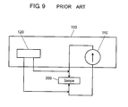
- FIG. 9 is a schematic diagram of a capacitor performance (capacitance) measuring instrument.
- Measuring circuit 100 includes constant current source 110 and oscilloscope 120 .
- Sample 200 which is a capacitor to find capacitance thereof, is connected to constant current source 110 .
- oscilloscope 120 for monitoring the voltage of sample 200 is connected to both ends of sample 200 .
- Capacitance C of capacitor can be measured by using the above measuring instrument. However, it is not realistic to build in the measuring instrument including an oscilloscope to the energy storage device used as a backup power supply. A configuration of collecting digital data of voltage V by an A/D converter can be built in the energy storage device. However, accuracy may be insufficient depending on specifications of energy storage device. Reasons are given below.
- the A/D converter is a 10-bit A/D converter and a level shifter is also built-in
- an assumed configuration is to capture voltage V at 10-bit resolution performance by amplifying input voltage ten times, for example, by the level shifter.
- the input voltage up to 5 V can be captured with about 4.9 mV (5V/(2 10 ⁇ 1)) at full scale. This resolution performance is called 1 LSB.
- a general A/D converter has an error of about ⁇ 5 LSB, and thus an output error of the above A/D converter is about ⁇ 0.49% ( ⁇ 5 LSB ⁇ 4.9 mV/5000 mV ⁇ 100). This error achieves a sufficient accuracy as a performance measuring instrument for measuring capacitance C of capacitor.
- Voltage V is a difference in absolute voltages at two points before and after period t. For example, if voltage V is 2V, absolute voltage values at two points whose difference is 2V, such as 48V to 50V, must be captured. An error at capturing 48V is, as described above, ⁇ 245 mV, and an error at capturing 50V is also ⁇ 245 mV. Therefore, an error of voltage V, which is a difference between these values, becomes ⁇ 490 mV at the maximum.
- an error may become ⁇ 490 mV at the maximum relative to 2V, which is voltage V.
- the error reaches ⁇ 24.5% ( ⁇ 0.49 V/2V ⁇ 100). Accordingly, if capacitance C is calculated using this voltage V, the error is large, and thus the determination accuracy of characteristic degradation is inadequate.
- An energy storage device of the present invention includes an energy storage section, a charging circuit, a first comparator, a second comparator, and control circuit.
- the charging circuit is electrically coupled to the energy storage section.
- the first comparator is electrically coupled to the energy storage section, and its output is inverted when voltage Vc of the energy storage section reaches first predetermined voltage Vc 1 .
- the second comparator is electrically coupled to the energy storage section, and its output is inverted when voltage Vc of the energy storage section reaches second predetermined voltage Vc 2 , which is greater than first predetermined voltage Vc 1 .
- the control circuit is electrically coupled to the charging circuit, the first comparator, and the second comparator.
- the control circuit obtains period tm from inversion of the output of the first comparator to inversion of the output of the second comparator when the energy storage section is charged with constant current Ics. Then, the control circuit calculates capacitance C of the energy storage section based on the period tm and voltage change width ⁇ Vc between predetermined first voltage Vc 1 and predetermined second voltage Vc 2 .
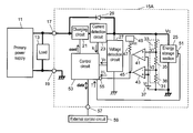
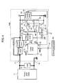
- FIG. 1 is a block circuit diagram of an energy storage device in accordance with a first exemplary embodiment of the present invention.
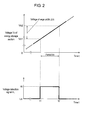
- FIG. 2 is a time-dependent characteristics chart of voltage Vc of an energy storage section and voltage detection signal HL of the energy storage device in FIG. 1 .
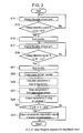
- FIG. 3 is a flow chart of an operation for calculating capacitance of the energy storage section and determining characteristic degradation in the energy storage device in FIG. 1 .
- FIG. 4 is a block circuit diagram of an energy storage device in accordance with a second exemplary embodiment of the present invention.
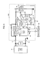
- FIG. 5 is a block circuit diagram of an energy storage device in accordance with a third exemplary embodiment of the present invention.
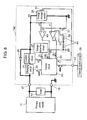
- FIG. 6 is a block circuit diagram of an energy storage device in accordance with a fourth exemplary embodiment of the present invention.
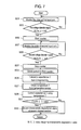
- FIG. 7 is a flow chart of an operation for calculating capacitance of the energy storage section and determining characteristic degradation in the energy storage device in FIG. 6 .
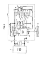
- FIG. 8 is a block circuit diagram of an energy storage device in accordance with a fifth exemplary embodiment of the present invention.
- FIG. 9 is a schematic diagram of a conventional capacitor performance measuring instrument.
- FIG. 1 is a block circuit diagram of an energy storage device in a first exemplary embodiment of the present invention.
- FIG. 2 is a time-dependent characteristics chart of voltage Vc of an energy storage section and voltage detection signal HL in the energy storage device shown in FIG. 1 .
- FIG. 3 is a flow chart of an operation for calculating capacitance of the energy storage section and determining characteristic degradation in the energy storage device shown in FIG. 1 .
- bold lines indicate power lines
- thin lines indicate signal lines.
- load 13 is connected in parallel to primary power supply 11
- energy storage device 15 A is connected in parallel to load 13 .
- Primary power supply 11 is a DC power source, and power is normally supplied from primary power supply 11 to load 13 .
- voltage of primary power supply 11 momentarily drops, power is supplied from energy storage device 15 A to load 13 , so as to continuously drive load 13 .
- Energy storage device 15 A includes energy storage section 25 , charging circuit 21 , first comparator 41 , second comparator 43 , and control circuit 53 .
- Charging circuit 21 is electrically coupled to energy storage section 25 .
- First comparator 41 is electrically coupled to energy storage section 25 , and its output is inverted when voltage Vc of energy storage section 25 reaches first predetermined voltage Vc 1 .
- Second comparator 43 is also electrically coupled to energy storage section 25 , and its output is inverted when voltage Vc of energy storage section 25 reaches second predetermined voltage Vc 2 , which is greater than first predetermined voltage Vc 1 .
- Control circuit 53 is electrically coupled to charging circuit 21 , first comparator 41 , and second comparator 43 .
- Energy storage device 15 A is electrically coupled to load 13 via positive terminal 17 and ground terminal 19 .
- Ground terminal 19 is electrically coupled such that it is in common with a ground inside energy storage device 15 A.
- energy storage section 25 that stores power is electrically coupled to positive terminal 17 via charging circuit 21 and current detection circuit 23 . Accordingly, charging circuit 21 charges energy storage section 25 . Charging circuit 21 is enough so that it can charge energy storage section 25 with constant current Ics. More specifically, a dropper circuit or DC/DC converter is applicable as charging circuit 21 . Since charging circuit 21 can charge energy storage section 25 with constant current Ics, capacitance C of energy storage section 25 can be easily identified. Energy storage section 25 is configured by connecting multiple electric double layer capacitors in series (25 pieces in this embodiment).
- Current detection circuit 23 detects current Ic charged to energy storage section 25 , and is used for control at charging energy storage section 25 with constant current Ics.
- current detection circuit 23 is configured with a shunt resistor and a differential amplifier (both are not illustrated), but is not limited to this configuration.
- current Ic may be electromagnetically detected using a hall element.
- Voltage detection circuit 27 is connected in parallel to energy storage section 25 .
- Voltage detection circuit 27 has a function to detect and output voltage Vc of energy storage section 25 .
- discharging circuit 29 for supplying power of energy storage section 25 to load 13 at the time of momentary voltage drop is electrically coupled between energy storage section 25 and positive terminal 17 .
- discharging circuit 29 is configured with a diode. If voltage of primary power supply 11 drops, the diode is turned on, and power of energy storage section 25 is supplied to load 13 . Configuration of discharging circuit 29 is not limited to a diode. A switch which can be externally controlled on and off, or a DC/DC converter is also applicable. If an interactive DC/DC converter is used, it can function as both charging circuit 21 and discharging circuit 29 .
- voltage-dividing circuit 31 is connected in parallel to energy storage section 25 .
- Voltage-dividing circuit 31 is configured with three voltage-dividing resistors. More specifically, voltage-dividing circuit 31 is configured with a series circuit of first voltage-dividing resistor 33 , second voltage-dividing resistor 35 , and third voltage-dividing resistor 36 from the side of positive terminal 17 . One end of third voltage-dividing resistor 36 is electrically coupled to ground terminal 19 . Since voltage-dividing circuit 31 is configured as above, voltage-dividing circuit 31 outputs first voltage V 1 proportional to voltage Vc of energy storage section 25 and second voltage V 2 proportional to voltage Vc but different from first voltage V 1 .
- first voltage V 1 is voltage between first voltage-dividing resistor 33 and second voltage-dividing resistor 35
- second voltage V 2 is voltage between second voltage-dividing resistor 35 and third voltage-dividing resistor 36 .
- First voltage V 1 output from voltage-dividing circuit 31 is input to first comparator 41 together with reference voltage Vr output from reference voltage source 37 .
- second voltage V 2 output from voltage-dividing circuit 31 is input to second comparator 43 together with reference voltage Vr.
- first comparator 41 and second comparator 43 are electrically coupled to energy storage section 25 in an indirect manner.
- first comparator 41 and second comparator 43 are configured with a so-called comparator (comparison circuit).
- a polarity of an input terminal of reference voltage Vr is negative for first comparator 41 , and positive for second comparator 43 .
- reference voltage source 37 a three-terminal regulator is applicable, for example.
- voltage-dividing circuit 31 By connecting energy storage section 25 to first comparator 41 and second comparator 43 via voltage-dividing circuit 31 , voltage-dividing circuit 31 reduces voltage Vc to the voltages proportional to voltage Vc even if voltage Vc is as high as, for example, about 50V at the maximum. Therefore, there is no need to use a high withstand voltage comparator for neither first comparator 41 nor second comparator 43 .
- first comparator 41 and an output of second comparator 43 are electrically coupled at contact point 45 .
- Contact point 45 is electrically coupled to pull-up voltage source 49 that has pull-up voltage Vcc via pull-up resistor 47 .
- This connection makes the voltage of contact point 45 a low voltage level (hereafter referred to as “Lo”) if at least one of the outputs of first comparator 41 and second comparator 43 is Lo close to 0.
- Both outputs of first comparator 41 and second comparator 43 are in a high-voltage level (hereafter referred to as “Hi”) close to 5V determined by pull-up voltage Vcc and resistance of pull-up resistor 47 , voltage of contact point 45 becomes Hi. Accordingly, voltage of contact point 45 becomes either Hi or Lo depending on first voltage V 1 and second voltage V 2 output from voltage-dividing circuit 31 .
- Temperature sensor 51 for detecting temperature T of energy storage section 25 is also provided in energy storage section 25 .
- temperature sensor 51 is provided inside a case (not illustrated) housing 25 of electric double layer capacitors.
- a thermistor that is highly sensitive to temperature is employed.
- temperature sensor 51 is not limited to the thermistor.
- Other elements such as a thermocouple, platinum temperature-sensing element, and pyroelectric sensor are also applicable.
- Charging circuit 21 , current detection circuit 23 , voltage detection circuit 27 , contact point 45 , and temperature sensor 51 are connected to control circuit 53 by signal lines, respectively.
- Control circuit 53 is configured with a microcomputer and peripheral circuits (both not illustrated), and reads current Ic from current detection circuit 23 , voltage Vc of energy storage section from voltage detection circuit 27 , and temperature T from temperature sensor 51 .
- contact point 45 is connected to input port 55 of control circuit 53 . Accordingly, voltage of contact point 45 that is Hi or Lo (hereafter referred to as “voltage detection signal HL”) is input to the microcomputer of control circuit 53 via input port 55 . Still more, control circuit 53 controls charging of energy storage section 25 by outputting control signal cont to charging circuit 21 .
- control circuit 53 is also connected to external control circuit 59 via data terminal 57 . Therefore, a range of pieces of data including current Ic, voltage Vc of energy storage section, temperature T, and operation state of energy storage device 15 A are exchanged between control circuit 53 and external control circuit 59 using data signal data.
- External control circuit 59 corresponds to an overall monitor device if energy storage device 15 A is used for backup of, for example, commercial AC power supply, and corresponds to a vehicle control circuit if energy storage device 15 A is used for cars.
- Control circuit 53 sends control signal cont to charging circuit 21 so as to charge energy storage section 25 if primary power supply 11 is operating normally and voltage Vc is not yet full-charge voltage (e.g., 50V). Upon receiving this signal, charging circuit 21 charges power of primary power supply 11 to energy storage section 25 .
- control circuit 53 charges energy storage section 25 with constant current Ics (e.g., 5 A) until voltage Vc of energy storage section 25 detected by voltage detection circuit 27 reaches the full-charge voltage.
- Control circuit 53 monitors current Ic detected by current detection circuit 23 , and controls charging circuit 21 , so as to charge energy storage section 25 with constant current Ics.
- control circuit 53 learns the state of normal operation of primary power supply 11 by data signal data from external control circuit 59 .
- a primary power supply voltage detection circuit (not illustrated) may be provided to positive terminal 17 to detect voltage of primary power supply 11 by control circuit 53 . This enables learning of the state of primary power supply 11 in a self-contained manner in energy storage device 15 A.
- control circuit 53 controls charging circuit 21 to apply a constant voltage to energy storage section 25 so that voltage Vc maintains fully charged voltage. This enables supply of power from energy storage section 25 to load 13 anytime when primary power supply 11 goes into a momentary voltage drop.
- charging circuit 29 configured with a diode is turned on. This is due to the voltage of primary power supply 11 falling below voltage Vc by the momentary voltage drop. As a result, power in energy storage section 25 is supplied to load 13 via discharging circuit 29 . Accordingly, since voltage Vc detected by voltage detection circuit 27 reduces, control circuit 53 detects this change, and outputs control signal cont to stop charging circuit 21 . This control reduces the possibility of backflow of the current output from discharging circuit 29 to the side of energy storage section 25 by charging circuit 21 .
- capacitance C can be calculated using Formula (I), based on voltage change width ⁇ Vc of voltage Vc of energy storage section 25 in period tm while energy storage section 25 is charged with constant current Ics. Since constant current Ics is a preset value, how to calculate period tm and voltage change width ⁇ Vc are described with reference to FIG. 2 .
- FIG. 2 is a time-dependent characteristics chart of voltage Vc of energy storage section 25 and voltage detection signal HL at charging energy storage section 25 . Since energy storage section 25 is charged with constant current Ics, voltage Vc and time t establishes a linear relationship. If voltage change width ⁇ Vc in certain period tm is obtained, capacitance C can be calculated using Formula (I). Period tm is duration of time from time t 1 to time t 2 , and ⁇ Vc is a voltage change width from first predetermined voltage Vc 1 to second predetermined voltage Vc 2 . It means a difference between second predetermined voltage Vc 2 and first predetermined voltage Vc 1 .
- Voltage-dividing circuit 31 outputs first voltage V 1 and second voltage V 2 from voltage Vc. These voltages and the same reference voltage Vr are input to first comparator 41 and second comparator 43 , respectively.
- first voltage V 1 is voltage between first voltage-dividing resistor 33 and second voltage-dividing resistor 35
- second voltage V 2 is voltage between second voltage-dividing resistor 31 and third voltage-dividing resistor 36 . Accordingly, it is apparent from the circuit in FIG. 1 that first voltage V 1 is higher than second voltage V 2 .
- First voltage-dividing resistor 33 , second voltage-dividing resistor 35 , and third voltage-dividing resistor 36 are all fixed resistors.
- Resistances of these resistors are predetermined such that first voltage V 1 reaches reference voltage Vr when voltage Vc of energy storage section 25 reaches first predetermined voltage Vc 1 , and second voltage V 2 reaches reference voltage Vr when voltage Vc reaches second predetermined voltage Vc 2 . On determining these resistances, it is considered that first voltage V 1 and second voltage V 2 fall within allowable input voltage of the comparators configuring first comparator 41 and second comparator 43 .
- first voltage V 1 and second voltage V 2 corresponds to voltage Vc
- first predetermined voltage Vc 1 and second predetermined voltage Vc 2 corresponds to reference voltage Vr.
- first voltage V 1 of voltage-dividing circuit 31 and reference voltage Vr corresponding to first predetermined voltage Vc 1 are input to first comparator 41 , and an output of first comparator 41 is inverted when voltage Vc (corresponding to first voltage V 1 ) reaches second predetermined voltage Vc 1 (corresponding to reference voltage Vr).
- second voltage V 2 of voltage-dividing circuit 31 and reference voltage Vr corresponding to second predetermined voltage Vc 2 are input to second comparator 43 , and an output of second comparator 43 is inverted when voltage Vc (corresponding to second voltage V 2 ) reaches second predetermined voltage Vc 2 (corresponding to reference voltage Vr).
- First predetermined voltage Vc 1 is set to 45V
- second predetermined voltage Vc 2 is set to 47V.
- these values are just an example. They are appropriately determined depending on a magnitude of constant current Ics and full-charge voltage of energy storage section 25 . If energy storage device 15 A is used as a backup power supply, energy storage device 15 A is normally almost full. Accordingly, if capacitance C is measured to find characteristic degradation in energy storage section 25 , it is preferable to set first predetermined voltage Vc 1 and second predetermined voltage Vc 2 close to the full-charge voltage. This enables application of sufficient voltage to load 13 by energy storage device 15 A even if momentary voltage drop occurs in primary power supply 11 at measuring capacitance C while energy storage device 15 A is in use.
- first voltage V 1 is higher than second voltage V 2
- the reference voltage Vr is the same for first comparator 41 and second comparator 43 . Therefore, if voltage Vc increases by charging energy storage section 25 , first voltage V 1 first reaches reference voltage Vr. This means that, as shown at time t 1 in FIG. 2 , voltage Vc has reached first predetermined voltage Vc 1 . As a result, the output of first comparator 41 is inverted from Lo to Hi. On the other hand, since second voltage V 2 has not yet reached reference voltage Vr, the output of second comparator 43 remains Hi. This is because reference voltage Vr is input to the positive side in second comparator 43 , which is opposite to first comparator 41 . The output of second comparator 43 remains Hi, if second voltage V 2 has not reached reference voltage Vr.
- first comparator 41 and second comparator 43 are connected at contact point 45 , and are pulled up by pull-up voltage source 49 . Accordingly, if both outputs of first comparator 41 and second comparator 43 are Hi, the voltage at contact point 45 , i.e., voltage detection signal HL, becomes Hi. This is indicated in FIG. 2 . If first voltage V 1 reaches reference voltage Vr at time t 1 , voltage detection signal HL is inverted from Lo to Hi.
- second voltage V 2 reaches reference voltage Vr. This is equivalent to the state that voltage Vc has reached second predetermined voltage Vc 2 at time t 2 in FIG. 2 .
- the output of second comparator 43 is inverted from Hi to Lo.
- voltage detection signal HL which is the voltage at contact point 45 , becomes Lo. In this way, if second voltage V 2 reaches reference voltage Vr at time t 2 , voltage detection signal HL is inverted from Hi to Lo.
- control circuit 53 obtains period tm from inversion of voltage detection signal HL in FIG. 2 . More specifically, control circuit 53 measures a duration of time from inversion of voltage detection signal HL at time t 1 to inversion again at time t 2 , using a counter (not illustrated) built-in in control circuit 53 to obtain period tm. This period tm is the same as the duration of time from inversion of the output of first comparator 41 to inversion of the output of second comparator 43 .
- capacitance C of energy storage section 25 can be calculated by assigning this period tm, and constant current Ics and voltage change width £Vc, which are already identified, to Formula (I).
- Capacitance C becomes smaller as characteristics of energy storage section 25 degrade. Therefore, if capacitance C is lower than a predetermined marginal characteristic degradation value, the characteristics of energy storage section 25 are determined to be degraded.
- control circuit 53 only needs to measure period tm, and thus the counter of microcomputer configuring control circuit 53 is used. Resolution performance of this counter is about a clock frequency of the microcomputer. Therefore, measurement accuracy of period tm is extremely high compared to the accuracy of conventional 10-bit A/D converter.
- first voltage V 1 and second voltage V 2 change.
- their change widths are almost equal.
- first voltage V 1 changes and first predetermined voltage Vc 1 which is calculated by inverse operation from first voltage V 1 , changes from 45V to 45.2V; second voltage V 2 also changes. Therefore, second predetermined voltage Vc 2 calculated by inverse operation changes from 47V to 47.2 V. Accordingly, voltage change width ⁇ Vc stays 2V in both cases before and after the change.
- Circuit configuration for calculating capacitance C in the way described above includes, as shown in FIG. 1 , voltage-dividing circuit 31 , first comparator 41 , second comparator 43 , pull-up resistor 47 , and pull-up voltage source 49 .
- This extremely simple circuit configuration enables calculation of capacitance C of energy storage section 25 with high accuracy.
- first voltage-dividing resistor 33 , second voltage-dividing resistor 35 , and third voltage-dividing resistor 36 are mounted at positions close to each other on the same circuit board. This arrangement further encourages changes of resistances of first voltage-dividing resistor 33 , second voltage-dividing resistor 35 , and third voltage-dividing resistor 36 in the same manner, depending on ambient temperature. Since there is only one reference voltage source 37 and pull-up voltage source 49 , they are not necessarily mounted on the same circuit board. However, from the view of structural simplification and downsizing of energy storage device 15 A by employing a single circuit board, it is preferable to mount these components also on the same circuit board.
- FIG. 3 shows a sub-routine executed as required from a main routine (not illustrated) of software built in control circuit 53 .
- control circuit 53 When the sub-routine in FIG. 3 is executed while charging energy storage section 25 with constant current Ics, control circuit 53 first monitors the state of input port 55 . Next, control circuit 53 determines whether or not voltage detection signal HL input to input port 55 is inverted from Lo to Hi (S 13 ). If no inversion takes place (No in S 13 ), the operation returns to S 11 , and control circuit 53 continues monitoring of the state of input port 55 .
- voltage detection signal HL is inverted (Yes in S 13 ), it means that first voltage V 1 has reached reference voltage Vr.
- control circuit 53 ignores any repeated inversion due to chattering of first comparator 41 in the subsequent operation until the sub-routine shown in FIG. 3 is completed.
- software hysteresis is given to voltage detection signal HL.
- this hysteresis may be set not to invert voltage again by a hardware system, once the voltage is inverted, until the voltage exceeds a predetermined voltage.
- control circuit 53 starts the counter built-in in its microcomputer (S 15 ). In FIG. 3 , the operations of S 11 and S 13 are repeated until voltage detection signal HL is inverted. However, if voltage detection signal HL is inverted in the middle of these operations, a slight gap in starting of the counter occurs. Accordingly, to calculate capacitance C with further higher accuracy, an interrupt is generated by inversion of voltage detection signal HL, and the counter starts at an interrupt destination.
- control circuit 53 monitors again the state of input port 55 (S 17 ), and determines whether or not voltage detection signal HL input to input port 55 is inverted from Hi to Lo (S 19 ). If no inversion takes place (No in S 19 ), the operation returns to S 17 , and control circuit 53 continues monitoring of the state of input port 55 .
- control circuit 53 determines that second voltage V 2 has reached reference voltage Vr. Same as above, software hysteresis is also given to this operation. Control circuit 53 stops the counter when Yes is selected in S 19 (S 21 ). To calculate capacitance C with further higher accuracy, an interrupt is generated by inversion of voltage detection signal HL, as described above, and the counter is stopped at an interrupt destination. Then, period tm is calculated based on a predetermined proportional constant between a counter value and time because the counter value is proportional to period tm (S 23 ).
- control circuit 53 calculates capacitance C of energy storage section 25 based on Formula (I) using calculated period tm (S 25 ). Constant current Ics and voltage change width ⁇ Vc, which are already identified values, are stored in a memory of the microcomputer in advance.
- a value of constant current Ics is stored in the memory, but current detection circuit 23 may be used for measuring current Ic as required.
- current detection circuit 23 may be used for measuring current Ic as required.
- the use of actual current value for calculating capacitance C enables calculation of capacitance with further higher accuracy.
- control circuit 53 obtains temperature T from temperature sensor 51 (S 27 ).
- Capacitance C is corrected based on correlation of temperature T and capacitance C stored in the memory in advance (S 29 ).
- Capacitance C and temperature T has a nonlinear correlation that capacitance C gradually declines when temperature T decreases. Accordingly, a change rate of capacitance C is calculated based on the correlation with present temperature T, and capacitance C is corrected based on temperature T by multiplying capacitance C calculated in S 25 by the change rate. This temperature correction improves the accuracy of determination of characteristic degradation described below.
- control circuit 53 compares capacitance C after temperature correction and marginal characteristic degradation value (S 31 ).
- the marginal characteristic degradation value is a marginal capacitance that energy storage device 15 A cannot be used no longer. This is determined in advance based on specifications of energy storage device 15 A, load 13 , and so on, and is stored in a memory. As already described, capacitance C reduces in line with characteristic degradation. Therefore, if capacitance C is equal to or below the marginal characteristic degradation value, control circuit 53 determines that characteristics of energy storage section 25 have degraded (Yes in S 31 ). In this case, control circuit 53 outputs the characteristic degradation signal of energy storage section 25 to external control circuit 59 as data signal data (S 33 ). Then, the sub-routine in FIG. 3 is completed, and the operation returns to the main routine. Upon receiving this characteristic degradation signal, external control circuit 59 alerts the user to replace energy storage section 25 or energy storage device 15 A through an operation such as alarming.
- control circuit 53 stops the operation for calculating capacitance C. More specifically, since control circuit 53 detects current Ic by current detection circuit 23 , current Ic momentarily changes if a momentary voltage drop occurs in primary power supply 11 . If this change is detected, control circuit 53 generates an interrupt to immediately stop execution of the sub-routine in FIG. 3 . This stops the operation for calculating capacitance C.
- This operation is executed because an error in period tm, in which voltage Vc of energy storage section 25 changes from first predetermined voltage Vc 1 to second predetermined voltage Vc 2 , occurs by the momentary voltage drop. Accordingly, an error in capacitance C is reduced to enable more accurate determination of characteristic degradation by stopping the operation for calculating capacitance C. Determination of occurrence of a momentary voltage drop is not limited to a change of current Ic. Voltage Vc of energy storage section 25 may be detected by voltage detection circuit 27 to determine occurrence of momentary voltage drop from this change.
- pull-up voltage source 49 is independent 1 y provided.
- driving voltage source (not illustrated) of first comparator 41 and second comparator 43 may be used commonly.
- the circuit configuration becomes simpler because there is no need to provide pull-up voltage source 49 independent 1 y .
- the microcomputer configured with a series circuit of pull-up voltage source 49 and pull-up resistor 47 connected to input port 55 inside control circuit 53 may be used for control circuit 53 . In this case, both pull-up voltage source 49 and pull-up resistor 47 become unnecessary. This further makes the circuit configuration further simpler.
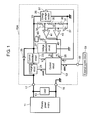
- FIG. 4 is a block circuit diagram of an energy storage device in a second exemplary embodiment of the present invention.
- bold lines indicate power lines, and thin lines indicate signal lines.
- Same reference marks are given to components same as those in FIG. 1 to omit their duplicate details.
- a characteristic structure of energy storage device 15 B in the second exemplary embodiment is as follows.
- voltage-dividing circuit 31 is a first voltage-dividing circuit that is connected in parallel to energy storage section 25 , and outputs first voltage V 1 smaller than voltage Vc.
- first reference voltage Vr 1 Voltage between two reference voltage-dividing resistors 61 (hereafter referred to as “first reference voltage Vr 1 ”) is input to first comparator 41 . More specifically, two reference voltage-dividing resistors 61 configure second voltage-dividing circuit 62 that is connected in parallel to the reference voltage source, and outputs first reference voltage Vr 1 in proportion to reference voltage Vr. First reference voltage Vr 1 is smaller than voltage Vr.
- first comparator 41 and second comparator 43 in FIG. 4 are different from those in FIG. 1 .
- reference voltage Vr input to second comparator 43 described in the first exemplary embodiment is called second reference voltage Vr 2 in this exemplary embodiment. Accordingly, reference voltage Vr and second reference voltage Vr 2 are equivalent.
- second reference voltage Vr 2 input to second comparator 43 is equivalent to reference voltage Vr. Accordingly, same as in the first exemplary embodiment, resistances of first voltage-dividing resistor 33 and third voltage-dividing resistor 36 are set in advance such that second voltage V 2 reaches second reference voltage Vr 2 when voltage Vc of energy storage section 25 reaches second predetermined voltage Vc 2 . In addition, it is considered that second voltage V 2 falls within an allowable input voltage of a comparator configuring second comparator 43 .
- first voltage V 1 and second voltage V 2 correspond to voltage Vc.
- first predetermined voltage Vc 1 and second predetermined voltage Vc 2 correspond to first reference voltage Vr 1 and second reference voltage Vr 2 , respectively.
- first voltage V 1 of voltage-dividing circuit 31 and first reference voltage Vr 1 corresponding to first predetermined voltage Vc 1 are input to first comparator 41 .
- voltage Vc corresponding to first voltage V 1 reaches first predetermined voltage Vc 1 corresponding to first reference voltage Vr 1 , the output of first comparator 41 is inverted.
- second voltage V 2 of voltage-dividing circuit 31 and second reference voltage Vr 2 corresponding to second predetermined voltage Vc 2 are input to second comparator 43 , respectively.
- voltage Vc corresponding to second voltage V 2 reaches second predetermined voltage Vc 2 corresponding to second reference voltage Vr 2 , the output of second comparator 43 is inverted.
- the operation for calculating capacitance C is the same as that shown in FIG. 3 in the first exemplary embodiment. If a momentary voltage drop occurs during execution of the sub-routine in FIG. 3 , the operation for calculating capacitance C is stopped. This is also the same as the first exemplary embodiment. Accordingly, highly accurate detection of capacitance C and determination of characteristic degradation in energy storage section 25 become feasible in the same way as the first exemplary embodiment.
- the structure in FIG. 4 allows reduction of the number of resistors used in voltage-dividing circuit 31 from three to two pieces, compared to that in FIG. 1 .
- three resistors are preferably disposed at nearby positions on the same circuit board, for example, so that their resistances change similarly against ambient temperature.
- the structure in FIG. 4 requires consideration to positions of only two resistors against ambient temperature for similar change in their resistances. Accordingly, design flexibility in component layout including resistors on a circuit board increases.
- two reference voltage-dividing resistors 61 also require positional consideration so that their resistances change similarly against ambient temperature.
- energy storage device 15 B that can detect capacitance C of energy storage section 25 with high accuracy is achievable with a simple structure.
- FIG. 5 is a block circuit diagram of an energy storage device in a third exemplary embodiment of the present invention.
- bold lines indicate power lines, and thin lines indicate signal lines. Same reference marks are given to components same as those in FIG. 4 to omit duplicate details.
- a characteristic structure of energy storage device 15 C in this exemplary embodiment, compared to that of the second exemplary embodiment, is as follows.
- Voltage Vc of energy storage section 25 is directly input to first comparator 41 and second comparator 43 . Accordingly, first voltage V 1 and second voltage V 2 are equivalent to voltage Vc.
- Resistances of two reference voltage-dividing resistors 61 are set such that voltage (first reference voltage Vr 1 ) between two reference voltage-dividing resistors 61 becomes 45V. Accordingly, first reference voltage Vr 1 is equivalent to first predetermined voltage Vc 1 .
- the operation for calculating capacitance C is the same as that in FIG. 3 in the first exemplary embodiment.
- the operation for stopping calculation of capacitance C when a momentary voltage drop occurs during execution of the sub-routine in FIG. 3 is also the same as that in the first exemplary embodiment. Accordingly, highly accurate detection of capacitance C and determination of characteristic degradation in energy storage section 25 become feasible in the same way as the first exemplary embodiment.
- FIG. 5 eliminates voltage-dividing circuit 31 , compared to the structure in FIG. 4 .
- the circuit configuration can thus be made simpler. However, expensive comparators for directly inputting high voltage are necessary.
- two reference voltage-dividing resistors 61 are preferably disposed at positions that their resistances change similarly against ambient temperature.
- energy storage device 15 C that can detect capacitance C of energy storage section 25 with high accuracy is achievable with a simple structure.
- FIG. 6 is a block circuit diagram of an energy storage device in a fourth exemplary embodiment of the present invention.
- FIG. 7 is a flow chart of the operation for determining characteristic degradation by calculating capacitance of the energy storage device in the fourth exemplary embodiment.
- bold lines indicate power lines
- thin lines indicate signal lines.
- same reference marks are given to components same as those in FIG. 1 to omit duplicate details.
- a characteristic structure of energy storage device 15 D in this exemplary embodiment, compared to that in the first exemplary embodiment is as follows.
- First input port 63 and second input port 65 are provided in control circuit 53 , instead of input port 55 .
- the output of first comparator 41 is connected to first input port 63 of control circuit 53
- the output of second comparator 43 is connected to second input port 65 of control circuit 53 independent 1 y.
- first voltage detection signal HL 1 the output of first comparator 41 (hereafter referred to as “first voltage detection signal HL 1 ”) is inverted first, and then the output of second comparator 43 (hereafter referred to as “second voltage detection signal HL 2 ”) is inverted. Since the two signals are independent 1 y input to control circuit 53 in this exemplary embodiment, the operation for determining characteristic degradation by calculating capacitance C of energy storage section 25 differs from the first exemplary embodiment in some points. The operation is described centering on these different points with reference to a flow chart (sub-routine) in FIG. 7 . The same operations in FIG. 7 and FIG. 3 are given the same step numbers to omit their duplicate details.
- control circuit 53 first monitors the state of first input port 63 (S 51 ). Next, control circuit 53 determines whether or not first voltage detection signal HL 1 input to first input port 63 is inverted from Lo to Hi. If not inverted (No in S 53 ), the operation returns to S 51 to continue monitoring of first input port 63 .
- first voltage detection signal HL 1 is inverted (Yes in S 53 ), it means that first voltage V 1 has reached reference voltage Vr.
- Control circuit 53 thus starts a counter built in a microcomputer of control circuit 53 (S 55 ).
- control circuit 53 monitors the state of second input port 65 (S 57 ), and determines whether or not second voltage detection signal HL 2 input to second input port 65 is inverted from Hi to Lo (S 59 ). If not inverted (No in S 59 ), the operation returns to S 57 , and control circuit 53 continues monitoring of second input port 65 .
- Second voltage detection signal HL 2 is inverted (Yes in S 59 ), it means that second voltage V 2 has reached reference voltage Vr.
- Control circuit 53 stops the counter (S 21 ).
- the operations of and after S 21 are the same as those in FIG. 3 , and thus their description is omitted.
- the operation for stopping calculation of capacitance C when a momentary voltage drop occurs during execution of the sub-routine in FIG. 7 is also the same as that in the first exemplary embodiment.
- hysteresis may be provided for determining inversion of first voltage detection signal HL 1 and second voltage detection signal HL 2 , or the counter may be started or stopped by an interrupt at occurrence of inversion.
- the configuration in this exemplary embodiment eliminates the need of pull-up resistor 47 and pull-up voltage source 49 , compared to the first exemplary embodiment. Accordingly, a further simpler circuit configuration is achievable. However, this configuration requires two input ports in control circuit 53 . Accordingly, adoption of the configuration in the first exemplary embodiment or the configuration in this exemplary embodiment is determined based on the available number of input ports.
- energy storage device 15 D that can detect capacitance C of energy storage section 25 with high accuracy is achievable with a simple structure.
- a layout of three resistors in voltage-dividing circuit 31 is preferably considered such that their resistances change similarly against ambient temperature. This is also the same as the first exemplary embodiment.
- voltage-dividing circuit 31 may be simplified by the use of two resistors, and two reference voltage voltage-dividing resistors 61 may be provided to reference voltage source 37 , same as those in the second exemplary embodiment. In this case, an effect is also the same as that in the second exemplary embodiment.
- first input port 63 and second input port 65 are independent in this exemplary embodiment. Therefore, outputs of first comparator 41 and second comparator 43 may be reversed. More specifically, first voltage detection signal HL 1 may be configured to invert either from Lo to Hi or Hi to Lo. This is also the same for second voltage detection signal HL 2 . Accordingly, a combination of inverted outputs of first voltage detection signal HL 1 and second voltage detection signal HL 2 may be selected as required.
- FIG. 8 is a block circuit diagram of an energy storage device in a fifth exemplary embodiment of the present invention.
- bold lines indicate power lines, and thin lines indicate signal lines.
- same reference marks are given to components same as those in FIGS. 5 and 6 to omit their duplicate details.
- a characteristic structure in the fifth exemplary embodiment is a combination of elimination of voltage-dividing circuit 31 from the configuration in the fourth exemplary embodiment, and provision of two reference voltage-dividing resistors 61 in reference voltage source 37 as in the third exemplary embodiment.
- first comparator 41 and second comparator 43 since voltage Vc of energy storage section 25 is directly input to first comparator 41 and second comparator 43 , high withstand voltage operational amplifiers are adopted.
- First voltage V 1 and second voltage V 2 are equivalent to voltage Vc of energy storage section 25 .
- resistances of two reference voltage-dividing resistors 61 are set such that second reference voltage Vr 2 becomes a high voltage of 47V, and first reference voltage Vr 1 becomes 45V. Accordingly, first reference voltage Vr 1 is equivalent to first predetermined voltage Vc 1 , and second reference voltage Vr 2 is equivalent to second predetermined voltage Vc 2 .
- Other components are the same as those in FIG. 6 .
- the operation for calculating capacitance C of energy storage device 15 E as configured above is the same as that in the fourth exemplary embodiment 4 in FIG. 7 .
- the operation for stopping calculation of capacitance C when a momentary voltage drop occurs during execution of the sub-routine in FIG. 7 is also the same as that in the first exemplary embodiment.
- the fifth exemplary embodiment also achieves highly accurate detection of capacitance C and determination of characteristic degradation in energy storage section 25 in the same way as the fourth exemplary embodiment.
- voltage-dividing circuit 31 In the configuration shown in FIG. 8 , voltage-dividing circuit 31 , pull-up resistor 47 , and pull-up voltage source 49 are unnecessary. Accordingly, detection of capacitance C with high accuracy becomes feasible with an extremely simple circuit configuration. However, more number of input ports is needed in control circuit 53 , and a change to high withstand voltage operational amplifiers is also required.
- two reference voltage-dividing resistors 61 are preferably disposed such that their resistances change similarly against ambient temperature in the same way as the second exemplary embodiment. Also same as the fourth exemplary embodiment, a combination of output inversion of first voltage detection signal HL 1 and second voltage detection signal HL 2 can be selected as required.
- energy storage device 15 E that can detect capacitance C of energy storage section 25 with high accuracy is achievable with a simple structure.
- polarities of input terminals of first comparator 41 and second comparator 43 are given as an example. They may be opposite. In that case, an inverting direction of outputs of first comparator 41 and second comparator 43 becomes opposite.
- Control circuit 53 also needs to determine inversion of voltage detection signal HL in a reversed way. In this case, depending on circuit configuration, resistance of voltage-dividing circuit 31 or resistance of reference voltage-dividing resistor 61 needs to be changed.
- the first to fifth exemplary embodiments refer to the configuration of providing temperature sensor 51 .
- temperature sensor 51 may not be provided if a change in ambient temperature is small, such as in the case of using energy storage device as an emergency power source. In this case, characteristic degradation is determined without applying temperature correction to calculated capacitance C.
- the first to fifth exemplary embodiments execute the operation for calculating capacitance C and determining characteristic degradation in energy storage section 25 during charging of energy storage section 25 with constant current Ics.
- capacitance C may be calculated and characteristic degradation may be determined during discharging with constant current Ics by providing a constant current discharging circuit (not illustrated) that is connected in parallel to energy storage section 25 and can discharge with constant current Ics.
- time-dependent characteristics of voltage Vc in FIG. 2 becomes a straight line declining rightward, but capacitance C is calculated in the same way as the first to fifth exemplary embodiments.
- This configuration of providing a constant current discharge circuit is effective when charging circuit 21 of energy storage section 25 is provided on the side of primary power supply, for example, and constant current charging cannot be controlled within the energy storage device, although characteristic degradation needs to be determined based on capacitance C. Also in this case, calculation of capacitance C is controlled to stop when a momentary voltage drop occurs during discharge. This achieves further accurate determination of characteristic degradation.
- first to fifth exemplary embodiments employ electric double layer capacitors for energy storage section 25 .
- This may be other capacitors such as electrochemical capacitor, or high-power battery.
- the energy storage device of the present invention has a simple structure, and can determine characteristic degradation by calculating capacitance of the energy storage section with high accuracy. Accordingly, the present invention is particularly applicable to an energy storage device for supplying power from its energy storage section at occurrence of a voltage drop in the primary power source.
Landscapes
- Engineering & Computer Science (AREA)
- Power Engineering (AREA)
- Charge And Discharge Circuits For Batteries Or The Like (AREA)
- Measurement Of Resistance Or Impedance (AREA)
- Tests Of Electric Status Of Batteries (AREA)
Abstract
Description
- 1. Field of the Invention
- The present invention relates to an energy storage device as a backup power supply for supplying power in its energy storage section to a load when voltage of a primary power supply reduces.
- 2. Background Art
- A primary power supply, which is a DC power supply, is formed of a rectifier circuit for rectifying commercial AC power supply or a car battery. An energy storage device as a backup power supply includes an energy storage element such as a capacitor, and makes up for voltage reduction by supplying power stored in the energy storage element to a load when the voltage of the primary power supply reduces. The load can thus continue its operation. This type of energy storage device is used for covering a momentary voltage drop in the primary power supply or as an emergency power supply. If characteristics of the energy storage element are degraded, the energy storage device may not be able to supply sufficient power to the load at occurrence of voltage drop. Therefore, it is important to determine characteristic degradation in the energy storage element.
- In general, if degradation in capacitor characteristics worsens, the storage capacity reduces, and thus capacitance becomes small. Accordingly, if a capacitor is used as the energy storage element, characteristic degradation can be determined by checking the capacitance.
- Next, an example of method of measuring capacitance of capacitor is described with reference to
FIG. 9 .FIG. 9 is a schematic diagram of a capacitor performance (capacitance) measuring instrument.Measuring circuit 100 includes constantcurrent source 110 andoscilloscope 120.Sample 200, which is a capacitor to find capacitance thereof, is connected to constantcurrent source 110. In addition,oscilloscope 120 for monitoring the voltage ofsample 200 is connected to both ends ofsample 200. - Capacitance C of
sample 200 is calculated as follows. If the current of constantcurrent source 110 is I, and voltage ofsample 200 that changes by charging during period t is V, the relationship of C·V=I·t is established. Since capacitance C and current I are constant, V=I·t/C is established. Voltage V shows a linear correlation with respect to period t. Accordingly, ifsample 200 is charged with constant current by constantcurrent source 110, its voltage linearly changes by time. Using this character,oscilloscope 120 measures a change in voltage V against period t, so as to measure capacitance C based on C=I·t/V. Alternatively, voltage V may be converted and measured in digital data by using an A/D converter, instead ofoscilloscope 120. - Capacitance C of capacitor can be measured by using the above measuring instrument. However, it is not realistic to build in the measuring instrument including an oscilloscope to the energy storage device used as a backup power supply. A configuration of collecting digital data of voltage V by an A/D converter can be built in the energy storage device. However, accuracy may be insufficient depending on specifications of energy storage device. Reasons are given below.
- In a configuration using an A/D converter instead of
oscilloscope 120 inFIG. 9 , variation of voltage V with time is measured up to the voltage lower (specifically, 0.3 V) than operating voltage of non-linear element in a circuit including the capacitor. Therefore, the A/D converter that can measure the voltage at least up to 0.3 V is sufficient. - On the other hand, if the A/D converter is a 10-bit A/D converter and a level shifter is also built-in, an assumed configuration is to capture voltage V at 10-bit resolution performance by amplifying input voltage ten times, for example, by the level shifter. In this case, the input voltage up to 5 V can be captured with about 4.9 mV (5V/(210−1)) at full scale. This resolution performance is called 1 LSB.
- A general A/D converter has an error of about ±5 LSB, and thus an output error of the above A/D converter is about ±0.49% (±5 LSB×4.9 mV/5000 mV×100). This error achieves a sufficient accuracy as a performance measuring instrument for measuring capacitance C of capacitor.
- On the other hand, if a load requiring backup power needs as high voltage as about 50V, for example, and the above general A/D converter is used for detecting high voltage, voltage V that can be captured is still up to 5V. Accordingly, voltage V needs to be input to the A/D converter after reducing one digit from a high-voltage value such as by applying resistive division. A captured voltage accuracy in this case becomes ±5 LSB×4.9 mV=±24.5 mV as described above. Therefore, a capture error is ten times, that is ±245 mV with respect to the high voltage (50V).
- If voltage V is calculated under this capture error, an error in voltage V becomes as follows. Voltage V is a difference in absolute voltages at two points before and after period t. For example, if voltage V is 2V, absolute voltage values at two points whose difference is 2V, such as 48V to 50V, must be captured. An error at capturing 48V is, as described above, ±245 mV, and an error at capturing 50V is also ±245 mV. Therefore, an error of voltage V, which is a difference between these values, becomes ±490 mV at the maximum.
- In other words, an error may become ±490 mV at the maximum relative to 2V, which is voltage V. In this case, the error reaches ±24.5% (±0.49 V/2V ×100). Accordingly, if capacitance C is calculated using this voltage V, the error is large, and thus the determination accuracy of characteristic degradation is inadequate.
- If voltage V is increased, the error becomes relatively small. However, period t becomes longer, which means more time is required for determining degradation by calculating capacitance C. Still more, one of absolute voltage values at two points needs to be a small value. If the voltage of primary power supply drops while charging from a low to high absolute voltage values, sufficient backup power many not be supplied.
- To increase the measuring accuracy of capacitance C, for example, resolution performance (number of bits) of A/D converter may be increased. However, this makes circuit configuration more complicated.
- An energy storage device of the present invention includes an energy storage section, a charging circuit, a first comparator, a second comparator, and control circuit. The charging circuit is electrically coupled to the energy storage section. The first comparator is electrically coupled to the energy storage section, and its output is inverted when voltage Vc of the energy storage section reaches first predetermined voltage Vc1. The second comparator is electrically coupled to the energy storage section, and its output is inverted when voltage Vc of the energy storage section reaches second predetermined voltage Vc2, which is greater than first predetermined voltage Vc1. The control circuit is electrically coupled to the charging circuit, the first comparator, and the second comparator. The control circuit obtains period tm from inversion of the output of the first comparator to inversion of the output of the second comparator when the energy storage section is charged with constant current Ics. Then, the control circuit calculates capacitance C of the energy storage section based on the period tm and voltage change width ΔVc between predetermined first voltage Vc1 and predetermined second voltage Vc2.
-
FIG. 1 is a block circuit diagram of an energy storage device in accordance with a first exemplary embodiment of the present invention. -
FIG. 2 is a time-dependent characteristics chart of voltage Vc of an energy storage section and voltage detection signal HL of the energy storage device inFIG. 1 . -
FIG. 3 is a flow chart of an operation for calculating capacitance of the energy storage section and determining characteristic degradation in the energy storage device inFIG. 1 . -
FIG. 4 is a block circuit diagram of an energy storage device in accordance with a second exemplary embodiment of the present invention. -
FIG. 5 is a block circuit diagram of an energy storage device in accordance with a third exemplary embodiment of the present invention. -
FIG. 6 is a block circuit diagram of an energy storage device in accordance with a fourth exemplary embodiment of the present invention. -
FIG. 7 is a flow chart of an operation for calculating capacitance of the energy storage section and determining characteristic degradation in the energy storage device inFIG. 6 . -
FIG. 8 is a block circuit diagram of an energy storage device in accordance with a fifth exemplary embodiment of the present invention. -
FIG. 9 is a schematic diagram of a conventional capacitor performance measuring instrument. -
FIG. 1 is a block circuit diagram of an energy storage device in a first exemplary embodiment of the present invention.FIG. 2 is a time-dependent characteristics chart of voltage Vc of an energy storage section and voltage detection signal HL in the energy storage device shown inFIG. 1 .FIG. 3 is a flow chart of an operation for calculating capacitance of the energy storage section and determining characteristic degradation in the energy storage device shown inFIG. 1 . InFIG. 1 , bold lines indicate power lines, and thin lines indicate signal lines. - As shown in
FIG. 1 , load 13 is connected in parallel toprimary power supply 11, andenergy storage device 15A is connected in parallel to load 13.Primary power supply 11 is a DC power source, and power is normally supplied fromprimary power supply 11 to load 13. When voltage ofprimary power supply 11 momentarily drops, power is supplied fromenergy storage device 15A to load 13, so as to continuously driveload 13. -
Energy storage device 15A includesenergy storage section 25, chargingcircuit 21,first comparator 41,second comparator 43, andcontrol circuit 53. Chargingcircuit 21 is electrically coupled toenergy storage section 25.First comparator 41 is electrically coupled toenergy storage section 25, and its output is inverted when voltage Vc ofenergy storage section 25 reaches first predetermined voltage Vc1.Second comparator 43 is also electrically coupled toenergy storage section 25, and its output is inverted when voltage Vc ofenergy storage section 25 reaches second predetermined voltage Vc2, which is greater than first predetermined voltage Vc1.Control circuit 53 is electrically coupled to chargingcircuit 21,first comparator 41, andsecond comparator 43. - Next, configuration including other components is detailed.
Energy storage device 15A is electrically coupled to load 13 viapositive terminal 17 andground terminal 19.Ground terminal 19 is electrically coupled such that it is in common with a ground insideenergy storage device 15A. - On the other hand,
energy storage section 25 that stores power is electrically coupled topositive terminal 17 via chargingcircuit 21 andcurrent detection circuit 23. Accordingly, chargingcircuit 21 chargesenergy storage section 25. Chargingcircuit 21 is enough so that it can chargeenergy storage section 25 with constant current Ics. More specifically, a dropper circuit or DC/DC converter is applicable as chargingcircuit 21. Since chargingcircuit 21 can chargeenergy storage section 25 with constant current Ics, capacitance C ofenergy storage section 25 can be easily identified.Energy storage section 25 is configured by connecting multiple electric double layer capacitors in series (25 pieces in this embodiment). -
Current detection circuit 23 detects current Ic charged toenergy storage section 25, and is used for control at chargingenergy storage section 25 with constant current Ics. In this exemplary embodiment,current detection circuit 23 is configured with a shunt resistor and a differential amplifier (both are not illustrated), but is not limited to this configuration. For example, current Ic may be electromagnetically detected using a hall element. -
Voltage detection circuit 27 is connected in parallel toenergy storage section 25.Voltage detection circuit 27 has a function to detect and output voltage Vc ofenergy storage section 25. In addition, dischargingcircuit 29 for supplying power ofenergy storage section 25 to load 13 at the time of momentary voltage drop is electrically coupled betweenenergy storage section 25 andpositive terminal 17. In this exemplary embodiment, dischargingcircuit 29 is configured with a diode. If voltage ofprimary power supply 11 drops, the diode is turned on, and power ofenergy storage section 25 is supplied to load 13. Configuration of dischargingcircuit 29 is not limited to a diode. A switch which can be externally controlled on and off, or a DC/DC converter is also applicable. If an interactive DC/DC converter is used, it can function as both chargingcircuit 21 and dischargingcircuit 29. - In addition, voltage-dividing
circuit 31 is connected in parallel toenergy storage section 25. Voltage-dividingcircuit 31 is configured with three voltage-dividing resistors. More specifically, voltage-dividingcircuit 31 is configured with a series circuit of first voltage-dividingresistor 33, second voltage-dividingresistor 35, and third voltage-dividingresistor 36 from the side ofpositive terminal 17. One end of third voltage-dividingresistor 36 is electrically coupled toground terminal 19. Since voltage-dividingcircuit 31 is configured as above, voltage-dividingcircuit 31 outputs first voltage V1 proportional to voltage Vc ofenergy storage section 25 and second voltage V2 proportional to voltage Vc but different from first voltage V1. Here, first voltage V1 is voltage between first voltage-dividingresistor 33 and second voltage-dividingresistor 35, and second voltage V2 is voltage between second voltage-dividingresistor 35 and third voltage-dividingresistor 36. - First voltage V1 output from voltage-dividing
circuit 31 is input tofirst comparator 41 together with reference voltage Vr output fromreference voltage source 37. In the same way, second voltage V2 output from voltage-dividingcircuit 31 is input tosecond comparator 43 together with reference voltage Vr. In this way,first comparator 41 andsecond comparator 43 are electrically coupled toenergy storage section 25 in an indirect manner. - Each of
first comparator 41 andsecond comparator 43 is configured with a so-called comparator (comparison circuit). A polarity of an input terminal of reference voltage Vr is negative forfirst comparator 41, and positive forsecond comparator 43. Asreference voltage source 37, a three-terminal regulator is applicable, for example. - By connecting
energy storage section 25 tofirst comparator 41 andsecond comparator 43 via voltage-dividingcircuit 31, voltage-dividingcircuit 31 reduces voltage Vc to the voltages proportional to voltage Vc even if voltage Vc is as high as, for example, about 50V at the maximum. Therefore, there is no need to use a high withstand voltage comparator for neitherfirst comparator 41 norsecond comparator 43. - An output of
first comparator 41 and an output ofsecond comparator 43 are electrically coupled atcontact point 45.Contact point 45 is electrically coupled to pull-upvoltage source 49 that has pull-up voltage Vcc via pull-upresistor 47. This connection makes the voltage of contact point 45 a low voltage level (hereafter referred to as “Lo”) if at least one of the outputs offirst comparator 41 andsecond comparator 43 is Lo close to 0. Both outputs offirst comparator 41 andsecond comparator 43 are in a high-voltage level (hereafter referred to as “Hi”) close to 5V determined by pull-up voltage Vcc and resistance of pull-upresistor 47, voltage ofcontact point 45 becomes Hi. Accordingly, voltage ofcontact point 45 becomes either Hi or Lo depending on first voltage V1 and second voltage V2 output from voltage-dividingcircuit 31. -
Temperature sensor 51 for detecting temperature T ofenergy storage section 25 is also provided inenergy storage section 25. In this exemplary embodiment,temperature sensor 51 is provided inside a case (not illustrated)housing 25 of electric double layer capacitors. Astemperature sensor 51, a thermistor that is highly sensitive to temperature is employed. However,temperature sensor 51 is not limited to the thermistor. Other elements such as a thermocouple, platinum temperature-sensing element, and pyroelectric sensor are also applicable. - Charging
circuit 21,current detection circuit 23,voltage detection circuit 27,contact point 45, andtemperature sensor 51 are connected to controlcircuit 53 by signal lines, respectively.Control circuit 53 is configured with a microcomputer and peripheral circuits (both not illustrated), and reads current Ic fromcurrent detection circuit 23, voltage Vc of energy storage section fromvoltage detection circuit 27, and temperature T fromtemperature sensor 51. In addition,contact point 45 is connected to inputport 55 ofcontrol circuit 53. Accordingly, voltage ofcontact point 45 that is Hi or Lo (hereafter referred to as “voltage detection signal HL”) is input to the microcomputer ofcontrol circuit 53 viainput port 55. Still more,control circuit 53 controls charging ofenergy storage section 25 by outputting control signal cont to chargingcircuit 21. Furthermore,control circuit 53 is also connected toexternal control circuit 59 viadata terminal 57. Therefore, a range of pieces of data including current Ic, voltage Vc of energy storage section, temperature T, and operation state ofenergy storage device 15A are exchanged betweencontrol circuit 53 andexternal control circuit 59 using data signal data.External control circuit 59 corresponds to an overall monitor device ifenergy storage device 15A is used for backup of, for example, commercial AC power supply, and corresponds to a vehicle control circuit ifenergy storage device 15A is used for cars. - Next, the operation of
energy storage device 15A is described. First, a basic operation ofenergy storage device 15A is described.Control circuit 53 sends control signal cont to chargingcircuit 21 so as to chargeenergy storage section 25 ifprimary power supply 11 is operating normally and voltage Vc is not yet full-charge voltage (e.g., 50V). Upon receiving this signal, chargingcircuit 21 charges power ofprimary power supply 11 toenergy storage section 25. Here,control circuit 53 chargesenergy storage section 25 with constant current Ics (e.g., 5A) until voltage Vc ofenergy storage section 25 detected byvoltage detection circuit 27 reaches the full-charge voltage.Control circuit 53 monitors current Ic detected bycurrent detection circuit 23, andcontrols charging circuit 21, so as to chargeenergy storage section 25 with constant current Ics. - In this exemplary embodiment,
control circuit 53 learns the state of normal operation ofprimary power supply 11 by data signal data fromexternal control circuit 59. Other than this, for example, a primary power supply voltage detection circuit (not illustrated) may be provided to positive terminal 17 to detect voltage ofprimary power supply 11 bycontrol circuit 53. This enables learning of the state ofprimary power supply 11 in a self-contained manner inenergy storage device 15A. - If
energy storage section 25 is fully charged,control circuit 53controls charging circuit 21 to apply a constant voltage toenergy storage section 25 so that voltage Vc maintains fully charged voltage. This enables supply of power fromenergy storage section 25 to load 13 anytime whenprimary power supply 11 goes into a momentary voltage drop. - If a momentary voltage drop occurs in
primary power supply 11, chargingcircuit 29 configured with a diode is turned on. This is due to the voltage ofprimary power supply 11 falling below voltage Vc by the momentary voltage drop. As a result, power inenergy storage section 25 is supplied to load 13 via dischargingcircuit 29. Accordingly, since voltage Vc detected byvoltage detection circuit 27 reduces,control circuit 53 detects this change, and outputs control signal cont to stop chargingcircuit 21. This control reduces the possibility of backflow of the current output from dischargingcircuit 29 to the side ofenergy storage section 25 by chargingcircuit 21. - If
primary power supply 11 recovers from the momentary voltage drop, voltage at the cathode side of dischargingcircuit 29 becomes high. Dischargingcircuit 29 thus automatically turns off. Accordingly, voltage Vc ofenergy storage section 25 approximately retains voltage at thetime discharging circuit 29 is turned off.Control circuit 53 detects this change in voltage Vc, andcontrols charging circuit 21 to fully chargeenergy storage section 25 again if discharge fromenergy storage section 25 is stopped andprimary power supply 11 resumes the normal operation. Repetition of these operations enables continuous driving ofload 13 even if voltage ofprimary power supply 11 momentarily drops. - Next is described how to calculate capacitance C of
energy storage section 25 and the operation for determining characteristic degradation based on the result in aboveenergy storage device 15A. - First, a measuring principle of capacitance C is the same as the prior art. More specifically, capacitance C can be calculated using Formula (I), based on voltage change width ΔVc of voltage Vc of
energy storage section 25 in period tm whileenergy storage section 25 is charged with constant current Ics. Since constant current Ics is a preset value, how to calculate period tm and voltage change width ΔVc are described with reference toFIG. 2 . -
C=Ics·tm/ΔVc (1) -
FIG. 2 is a time-dependent characteristics chart of voltage Vc ofenergy storage section 25 and voltage detection signal HL at chargingenergy storage section 25. Sinceenergy storage section 25 is charged with constant current Ics, voltage Vc and time t establishes a linear relationship. If voltage change width ΔVc in certain period tm is obtained, capacitance C can be calculated using Formula (I). Period tm is duration of time from time t1 to time t2, and ΔVc is a voltage change width from first predetermined voltage Vc1 to second predetermined voltage Vc2. It means a difference between second predetermined voltage Vc2 and first predetermined voltage Vc1. - Next is described how to obtain voltage change width ΔVc and period tm in this exemplary embodiment. Voltage-dividing
circuit 31 outputs first voltage V1 and second voltage V2 from voltage Vc. These voltages and the same reference voltage Vr are input tofirst comparator 41 andsecond comparator 43, respectively. As previously described, first voltage V1 is voltage between first voltage-dividingresistor 33 and second voltage-dividingresistor 35, and second voltage V2 is voltage between second voltage-dividingresistor 31 and third voltage-dividingresistor 36. Accordingly, it is apparent from the circuit inFIG. 1 that first voltage V1 is higher than second voltage V2. First voltage-dividingresistor 33, second voltage-dividingresistor 35, and third voltage-dividingresistor 36 are all fixed resistors. Resistances of these resistors are predetermined such that first voltage V1 reaches reference voltage Vr when voltage Vc ofenergy storage section 25 reaches first predetermined voltage Vc1, and second voltage V2 reaches reference voltage Vr when voltage Vc reaches second predetermined voltage Vc2. On determining these resistances, it is considered that first voltage V1 and second voltage V2 fall within allowable input voltage of the comparators configuringfirst comparator 41 andsecond comparator 43. - By determining the resistances in this way, first voltage V1 and second voltage V2 corresponds to voltage Vc, and first predetermined voltage Vc1 and second predetermined voltage Vc2 corresponds to reference voltage Vr. Accordingly, first voltage V1 of voltage-dividing
circuit 31 and reference voltage Vr corresponding to first predetermined voltage Vc1 are input tofirst comparator 41, and an output offirst comparator 41 is inverted when voltage Vc (corresponding to first voltage V1) reaches second predetermined voltage Vc1 (corresponding to reference voltage Vr). In the same way, second voltage V2 of voltage-dividingcircuit 31 and reference voltage Vr corresponding to second predetermined voltage Vc2 are input tosecond comparator 43, and an output ofsecond comparator 43 is inverted when voltage Vc (corresponding to second voltage V2) reaches second predetermined voltage Vc2 (corresponding to reference voltage Vr). - First predetermined voltage Vc1 is set to 45V, and second predetermined voltage Vc2 is set to 47V. However, these values are just an example. They are appropriately determined depending on a magnitude of constant current Ics and full-charge voltage of
energy storage section 25. Ifenergy storage device 15A is used as a backup power supply,energy storage device 15A is normally almost full. Accordingly, if capacitance C is measured to find characteristic degradation inenergy storage section 25, it is preferable to set first predetermined voltage Vc1 and second predetermined voltage Vc2 close to the full-charge voltage. This enables application of sufficient voltage to load 13 byenergy storage device 15A even if momentary voltage drop occurs inprimary power supply 11 at measuring capacitance C whileenergy storage device 15A is in use. - As described above, first voltage V1 is higher than second voltage V2, the reference voltage Vr is the same for
first comparator 41 andsecond comparator 43. Therefore, if voltage Vc increases by chargingenergy storage section 25, first voltage V1 first reaches reference voltage Vr. This means that, as shown at time t1 inFIG. 2 , voltage Vc has reached first predetermined voltage Vc1. As a result, the output offirst comparator 41 is inverted from Lo to Hi. On the other hand, since second voltage V2 has not yet reached reference voltage Vr, the output ofsecond comparator 43 remains Hi. This is because reference voltage Vr is input to the positive side insecond comparator 43, which is opposite tofirst comparator 41. The output ofsecond comparator 43 remains Hi, if second voltage V2 has not reached reference voltage Vr. - As described above, the outputs of
first comparator 41 andsecond comparator 43 are connected atcontact point 45, and are pulled up by pull-upvoltage source 49. Accordingly, if both outputs offirst comparator 41 andsecond comparator 43 are Hi, the voltage atcontact point 45, i.e., voltage detection signal HL, becomes Hi. This is indicated inFIG. 2 . If first voltage V1 reaches reference voltage Vr at time t1, voltage detection signal HL is inverted from Lo to Hi. - Next, if charging of
energy storage section 25 continues, second voltage V2 reaches reference voltage Vr. This is equivalent to the state that voltage Vc has reached second predetermined voltage Vc2 at time t2 inFIG. 2 . As a result, the output ofsecond comparator 43 is inverted from Hi to Lo. On the other hand, since first voltage V1 has already reached reference voltage Vr, the output offirst comparator 41 remains Hi. Therefore, voltage detection signal HL, which is the voltage atcontact point 45, becomes Lo. In this way, if second voltage V2 reaches reference voltage Vr at time t2, voltage detection signal HL is inverted from Hi to Lo. - Since first predetermined voltage Vc1 and second predetermined voltage Vc2 are determined in advance, voltage change width ΔVc can also be obtained in advance. Therefore,
control circuit 53 obtains period tm from inversion of voltage detection signal HL inFIG. 2 . More specifically,control circuit 53 measures a duration of time from inversion of voltage detection signal HL at time t1 to inversion again at time t2, using a counter (not illustrated) built-in incontrol circuit 53 to obtain period tm. This period tm is the same as the duration of time from inversion of the output offirst comparator 41 to inversion of the output ofsecond comparator 43. - By obtaining period tm in this way, capacitance C of
energy storage section 25 can be calculated by assigning this period tm, and constant current Ics and voltage change width £Vc, which are already identified, to Formula (I). Capacitance C becomes smaller as characteristics ofenergy storage section 25 degrade. Therefore, if capacitance C is lower than a predetermined marginal characteristic degradation value, the characteristics ofenergy storage section 25 are determined to be degraded. - If capacitance C is calculated in this way, characteristic degradation can be more accurately determined due to the next reasons. First,
control circuit 53 only needs to measure period tm, and thus the counter of microcomputer configuringcontrol circuit 53 is used. Resolution performance of this counter is about a clock frequency of the microcomputer. Therefore, measurement accuracy of period tm is extremely high compared to the accuracy of conventional 10-bit A/D converter. - Still more, as resistances of first voltage-dividing
resistor 33, second voltage-dividingresistor 35, and third voltage-dividingresistor 36 change such as by ambient temperature, first voltage V1 and second voltage V2 also change. However, their change widths are almost equal. In other words, for example, if first voltage V1 changes and first predetermined voltage Vc1, which is calculated by inverse operation from first voltage V1, changes from 45V to 45.2V; second voltage V2 also changes. Therefore, second predetermined voltage Vc2 calculated by inverse operation changes from 47V to 47.2 V. Accordingly, voltage change width ΔVc stays 2V in both cases before and after the change. - Furthermore, even if reference voltage Vr changes, period tm is constant, although inversion time of voltage detection signal HL changes. This is because reference voltage Vr is input to both of
first comparator 41 andsecond comparator 43. Accordingly, for calculating capacitance C, only a binary signal (voltage detection signal HL) of whether or not the voltage has reached first predetermined voltage Vc1 and second predetermined voltage Vc2 is needed without directly detecting voltage Vc ofenergy storage section 25. Therefore, capacitance C can be more accurately calculated by eliminating a cause of error of the conventional A/D converter. - Circuit configuration for calculating capacitance C in the way described above includes, as shown in
FIG. 1 , voltage-dividingcircuit 31,first comparator 41,second comparator 43, pull-upresistor 47, and pull-upvoltage source 49. This extremely simple circuit configuration enables calculation of capacitance C ofenergy storage section 25 with high accuracy. - To calculate capacitance C with further higher accuracy, for example, first voltage-dividing
resistor 33, second voltage-dividingresistor 35, and third voltage-dividingresistor 36 are mounted at positions close to each other on the same circuit board. This arrangement further encourages changes of resistances of first voltage-dividingresistor 33, second voltage-dividingresistor 35, and third voltage-dividingresistor 36 in the same manner, depending on ambient temperature. Since there is only onereference voltage source 37 and pull-upvoltage source 49, they are not necessarily mounted on the same circuit board. However, from the view of structural simplification and downsizing ofenergy storage device 15A by employing a single circuit board, it is preferable to mount these components also on the same circuit board. - Next is described the operation for determining characteristic degradation by calculating capacitance C of
energy storage device 15A with reference to a flow chart inFIG. 3 .FIG. 3 shows a sub-routine executed as required from a main routine (not illustrated) of software built incontrol circuit 53. - When the sub-routine in
FIG. 3 is executed while chargingenergy storage section 25 with constant current Ics,control circuit 53 first monitors the state ofinput port 55. Next,control circuit 53 determines whether or not voltage detection signal HL input to inputport 55 is inverted from Lo to Hi (S13). If no inversion takes place (No in S13), the operation returns to S11, andcontrol circuit 53 continues monitoring of the state ofinput port 55. - On the other hand, if voltage detection signal HL is inverted (Yes in S13), it means that first voltage V1 has reached reference voltage Vr. Once voltage detection signal HL is inverted,
control circuit 53 ignores any repeated inversion due to chattering offirst comparator 41 in the subsequent operation until the sub-routine shown inFIG. 3 is completed. Through this operation, software hysteresis is given to voltage detection signal HL. Alternatively, this hysteresis may be set not to invert voltage again by a hardware system, once the voltage is inverted, until the voltage exceeds a predetermined voltage. - If first voltage V1 reaches reference voltage Vr by Yes in S13,
control circuit 53 starts the counter built-in in its microcomputer (S15). InFIG. 3 , the operations of S11 and S13 are repeated until voltage detection signal HL is inverted. However, if voltage detection signal HL is inverted in the middle of these operations, a slight gap in starting of the counter occurs. Accordingly, to calculate capacitance C with further higher accuracy, an interrupt is generated by inversion of voltage detection signal HL, and the counter starts at an interrupt destination. - Next,
control circuit 53 monitors again the state of input port 55 (S17), and determines whether or not voltage detection signal HL input to inputport 55 is inverted from Hi to Lo (S19). If no inversion takes place (No in S19), the operation returns to S17, andcontrol circuit 53 continues monitoring of the state ofinput port 55. - On the other hand, if voltage detection signal HL is inverted (Yes in S19),
control circuit 53 determines that second voltage V2 has reached reference voltage Vr. Same as above, software hysteresis is also given to this operation.Control circuit 53 stops the counter when Yes is selected in S19 (S21). To calculate capacitance C with further higher accuracy, an interrupt is generated by inversion of voltage detection signal HL, as described above, and the counter is stopped at an interrupt destination. Then, period tm is calculated based on a predetermined proportional constant between a counter value and time because the counter value is proportional to period tm (S23). - Next,
control circuit 53 calculates capacitance C ofenergy storage section 25 based on Formula (I) using calculated period tm (S25). Constant current Ics and voltage change width ΔVc, which are already identified values, are stored in a memory of the microcomputer in advance. - In this exemplary embodiment, a value of constant current Ics is stored in the memory, but
current detection circuit 23 may be used for measuring current Ic as required. In this case, the use of actual current value for calculating capacitance C enables calculation of capacitance with further higher accuracy. - Then, control
circuit 53 obtains temperature T from temperature sensor 51 (S27). Capacitance C is corrected based on correlation of temperature T and capacitance C stored in the memory in advance (S29). Capacitance C and temperature T has a nonlinear correlation that capacitance C gradually declines when temperature T decreases. Accordingly, a change rate of capacitance C is calculated based on the correlation with present temperature T, and capacitance C is corrected based on temperature T by multiplying capacitance C calculated in S25 by the change rate. This temperature correction improves the accuracy of determination of characteristic degradation described below. - Next,
control circuit 53 compares capacitance C after temperature correction and marginal characteristic degradation value (S31). The marginal characteristic degradation value is a marginal capacitance thatenergy storage device 15A cannot be used no longer. This is determined in advance based on specifications ofenergy storage device 15A,load 13, and so on, and is stored in a memory. As already described, capacitance C reduces in line with characteristic degradation. Therefore, if capacitance C is equal to or below the marginal characteristic degradation value,control circuit 53 determines that characteristics ofenergy storage section 25 have degraded (Yes in S31). In this case,control circuit 53 outputs the characteristic degradation signal ofenergy storage section 25 toexternal control circuit 59 as data signal data (S33). Then, the sub-routine inFIG. 3 is completed, and the operation returns to the main routine. Upon receiving this characteristic degradation signal,external control circuit 59 alerts the user to replaceenergy storage section 25 orenergy storage device 15A through an operation such as alarming. - On the other hand, if capacitance C exceeds the marginal characteristic degradation value (No in S31),
energy storage section 25 have not degraded, the sub-routine is completed, and the operation returns to the main routine. - By repeating these operations every time
energy storage section 25 is charged, characteristic degradation inenergy storage section 25 can be determined with high accuracy, and reliability ofenergy storage device 15A thus increases. - While capacitance C is calculated in the sub-routine, and characteristic degradation in
energy storage section 25 is determined, charging ofenergy storage section 25 with constant current Ics may be interrupted due to a momentary voltage drop ofprimary power supply 11. In this case,control circuit 53 stops the operation for calculating capacitance C. More specifically, sincecontrol circuit 53 detects current Ic bycurrent detection circuit 23, current Ic momentarily changes if a momentary voltage drop occurs inprimary power supply 11. If this change is detected,control circuit 53 generates an interrupt to immediately stop execution of the sub-routine inFIG. 3 . This stops the operation for calculating capacitance C. This operation is executed because an error in period tm, in which voltage Vc ofenergy storage section 25 changes from first predetermined voltage Vc1 to second predetermined voltage Vc2, occurs by the momentary voltage drop. Accordingly, an error in capacitance C is reduced to enable more accurate determination of characteristic degradation by stopping the operation for calculating capacitance C. Determination of occurrence of a momentary voltage drop is not limited to a change of current Ic. Voltage Vc ofenergy storage section 25 may be detected byvoltage detection circuit 27 to determine occurrence of momentary voltage drop from this change. - With the above structure and operations, capacitance C of
energy storage section 25 can be detected with high accuracy using a simple structure. In this exemplary embodiment, pull-upvoltage source 49 is independent1 y provided. However, for example, driving voltage source (not illustrated) offirst comparator 41 andsecond comparator 43 may be used commonly. In this case, the circuit configuration becomes simpler because there is no need to provide pull-upvoltage source 49 independent1 y. In addition, the microcomputer configured with a series circuit of pull-upvoltage source 49 and pull-upresistor 47 connected to inputport 55 insidecontrol circuit 53 may be used forcontrol circuit 53. In this case, both pull-upvoltage source 49 and pull-upresistor 47 become unnecessary. This further makes the circuit configuration further simpler. -
FIG. 4 is a block circuit diagram of an energy storage device in a second exemplary embodiment of the present invention. InFIG. 4 , bold lines indicate power lines, and thin lines indicate signal lines. Same reference marks are given to components same as those inFIG. 1 to omit their duplicate details. In other words, a characteristic structure ofenergy storage device 15B in the second exemplary embodiment is as follows. - 1) In voltage-dividing
circuit 31, second voltage-dividingresistor 35 is removed, and first voltage-dividingresistor 33 and third voltage-dividingresistor 36 are connected in series. More specifically, voltage-dividingcircuit 31 is a first voltage-dividing circuit that is connected in parallel toenergy storage section 25, and outputs first voltage V1 smaller than voltage Vc. - 2) Voltage between first voltage-dividing
resistor 33 and third voltage-dividingresistor 36 is input tofirst comparator 41 andsecond comparator 43. Accordingly, voltages input from voltage-dividingcircuit 31 tofirst comparator 41 andsecond comparator 43 become equivalent. (First voltage V1=Second voltage V2). - 3) Series-connected two reference voltage-dividing
resistors 61 are provided between the positive side ofreference voltage source 37 and ground. - 4) Voltage between two reference voltage-dividing resistors 61 (hereafter referred to as “first reference voltage Vr1”) is input to
first comparator 41. More specifically, two reference voltage-dividingresistors 61 configure second voltage-dividingcircuit 62 that is connected in parallel to the reference voltage source, and outputs first reference voltage Vr1 in proportion to reference voltage Vr. First reference voltage Vr1 is smaller than voltage Vr. - Components other than the above are the same as that in the first exemplary embodiment. Positions of
first comparator 41 andsecond comparator 43 inFIG. 4 are different from those inFIG. 1 . In addition, reference voltage Vr input tosecond comparator 43 described in the first exemplary embodiment is called second reference voltage Vr2 in this exemplary embodiment. Accordingly, reference voltage Vr and second reference voltage Vr2 are equivalent. - When the configuration in
FIG. 4 is compared with the that inFIG. 1 , voltages input from voltage-dividingcircuit 31 tofirst comparator 41 andsecond comparator 43 become equivalent in the configuration inFIG. 4 . And, voltages input fromreference voltage source 37 tofirst comparator 41 andsecond comparator 43 become different in this configuration inFIG. 4 . The operation for inverting outputs offirst comparator 41 andsecond comparator 43 in this exemplary embodiment is as follows. - First, second reference voltage Vr2 input to
second comparator 43 is equivalent to reference voltage Vr. Accordingly, same as in the first exemplary embodiment, resistances of first voltage-dividingresistor 33 and third voltage-dividingresistor 36 are set in advance such that second voltage V2 reaches second reference voltage Vr2 when voltage Vc ofenergy storage section 25 reaches second predetermined voltage Vc2. In addition, it is considered that second voltage V2 falls within an allowable input voltage of a comparator configuringsecond comparator 43. - Next, first voltage V1 input to
first comparator 41 is equivalent to second voltage V2. Accordingly, resistances of two reference voltage-dividingresistors 61 are set such that first voltage V1 reaches first reference voltage Vr1 when voltage Vc ofenergy storage section 25 reaches first predetermined voltage Vc1. It is apparent from the circuit inFIG. 4 that first reference voltage Vr1 is lower than second reference voltage Vr2 (=Reference voltage Vr), and thus an output offirst comparator 41 is inverted before an output ofsecond comparator 43 is inverted. - By setting resistances of first voltage-dividing
resistor 33, third voltage-dividingresistor 36, and two reference voltage-dividingresistors 61 in this way, first voltage V1 and second voltage V2 correspond to voltage Vc. And, first predetermined voltage Vc1 and second predetermined voltage Vc2 correspond to first reference voltage Vr1 and second reference voltage Vr2, respectively. Accordingly, first voltage V1 of voltage-dividingcircuit 31 and first reference voltage Vr1 corresponding to first predetermined voltage Vc1 are input tofirst comparator 41. When voltage Vc corresponding to first voltage V1 reaches first predetermined voltage Vc1 corresponding to first reference voltage Vr1, the output offirst comparator 41 is inverted. In the same way, second voltage V2 of voltage-dividingcircuit 31 and second reference voltage Vr2 corresponding to second predetermined voltage Vc2 are input tosecond comparator 43, respectively. When voltage Vc corresponding to second voltage V2 reaches second predetermined voltage Vc2 corresponding to second reference voltage Vr2, the output ofsecond comparator 43 is inverted. - In
energy storage device 15B as configured above, the operation for calculating capacitance C is the same as that shown inFIG. 3 in the first exemplary embodiment. If a momentary voltage drop occurs during execution of the sub-routine inFIG. 3 , the operation for calculating capacitance C is stopped. This is also the same as the first exemplary embodiment. Accordingly, highly accurate detection of capacitance C and determination of characteristic degradation inenergy storage section 25 become feasible in the same way as the first exemplary embodiment. - The structure in
FIG. 4 allows reduction of the number of resistors used in voltage-dividingcircuit 31 from three to two pieces, compared to that inFIG. 1 . InFIG. 1 , three resistors are preferably disposed at nearby positions on the same circuit board, for example, so that their resistances change similarly against ambient temperature. On the other hand, the structure inFIG. 4 requires consideration to positions of only two resistors against ambient temperature for similar change in their resistances. Accordingly, design flexibility in component layout including resistors on a circuit board increases. However, two reference voltage-dividingresistors 61 also require positional consideration so that their resistances change similarly against ambient temperature. However, there is no need to dispose all of the resistors used in voltage-dividingcircuit 31 and two reference voltage-dividingresistors 61 at nearby positions on the circuit board. - With the above configuration and operation,
energy storage device 15B that can detect capacitance C ofenergy storage section 25 with high accuracy is achievable with a simple structure. -
FIG. 5 is a block circuit diagram of an energy storage device in a third exemplary embodiment of the present invention. InFIG. 5 , bold lines indicate power lines, and thin lines indicate signal lines. Same reference marks are given to components same as those inFIG. 4 to omit duplicate details. In other words, a characteristic structure ofenergy storage device 15C in this exemplary embodiment, compared to that of the second exemplary embodiment, is as follows. - 1) Voltage-dividing
circuit 31 is eliminated - 2) Voltage Vc of
energy storage section 25 is directly input tofirst comparator 41 andsecond comparator 43. Accordingly, first voltage V1 and second voltage V2 are equivalent to voltage Vc. - 3) Since voltage Vc is directly input to
first comparator 41 andsecond comparator 43, high withstand voltage comparator are employed asfirst comparator 41 andsecond comparator 43. - 4) Reference voltage Vr (=Second reference voltage Vr2) of
reference voltage source 37 is set to a high voltage of 47V. Accordingly, second reference voltage Vr2 becomes equivalent to second predetermined voltage Vc2. - 5) Resistances of two reference voltage-dividing
resistors 61 are set such that voltage (first reference voltage Vr1) between two reference voltage-dividingresistors 61 becomes 45V. Accordingly, first reference voltage Vr1 is equivalent to first predetermined voltage Vc1. - Components other than the above are the same as that in
FIG. 4 . With the above structural changes, the operation for inverting the outputs offirst comparator 41 andsecond comparator 43 is as follows in this exemplary embodiment. - First, first voltage V1 (=Voltage Vc) and first reference voltage Vr1 (=First predetermined voltage Vc1) are input to
first comparator 41, respectively. Accordingly, the output offirst comparator 41 is inverted when voltage Vc (=First voltage V1) reaches first predetermined voltage Vc1 (=First reference voltage Vr1). On the other hand, second voltage V2 (=Voltage Vc) and second reference voltage Vr2 (=Second predetermined voltage Vc2) are input tosecond comparator 43, respectively. Accordingly, the output ofsecond comparator 43 is inverted when voltage Vc (=Second voltage V2) reaches second predetermined voltage Vc2 (=Second reference voltage Vr2). - In
energy storage device 15C as configured above, the operation for calculating capacitance C is the same as that inFIG. 3 in the first exemplary embodiment. The operation for stopping calculation of capacitance C when a momentary voltage drop occurs during execution of the sub-routine inFIG. 3 is also the same as that in the first exemplary embodiment. Accordingly, highly accurate detection of capacitance C and determination of characteristic degradation inenergy storage section 25 become feasible in the same way as the first exemplary embodiment. - The structure in
FIG. 5 eliminates voltage-dividingcircuit 31, compared to the structure inFIG. 4 . The circuit configuration can thus be made simpler. However, expensive comparators for directly inputting high voltage are necessary. Same as the second exemplary embodiment, two reference voltage-dividingresistors 61 are preferably disposed at positions that their resistances change similarly against ambient temperature. - With the above configuration and operation,
energy storage device 15C that can detect capacitance C ofenergy storage section 25 with high accuracy is achievable with a simple structure. -
FIG. 6 is a block circuit diagram of an energy storage device in a fourth exemplary embodiment of the present invention.FIG. 7 is a flow chart of the operation for determining characteristic degradation by calculating capacitance of the energy storage device in the fourth exemplary embodiment. InFIG. 6 , bold lines indicate power lines, and thin lines indicate signal lines. InFIG. 6 , same reference marks are given to components same as those inFIG. 1 to omit duplicate details. In other words, a characteristic structure ofenergy storage device 15D in this exemplary embodiment, compared to that in the first exemplary embodiment, is as follows. - 1)
First input port 63 andsecond input port 65 are provided incontrol circuit 53, instead ofinput port 55. The output offirst comparator 41 is connected tofirst input port 63 ofcontrol circuit 53, and the output ofsecond comparator 43 is connected tosecond input port 65 ofcontrol circuit 53 independent1 y. - 2) Pull-up
resistor 47 and pull-upvoltage source 49 are eliminated. - 3) As a result, outputs of
first comparator 41 andsecond comparator 43 are not pulled up. Accordingly,first comparator 41 andsecond comparator 43 are changed from comparators to operational amplifiers. - Other components are the same as those in
FIG. 1 . The above changes in the configuration also achieve the operation for inverting the outputs offirst comparator 41 andsecond comparator 43 in the same way as the first exemplary embodiment. - As
energy storage section 25 is charged, the output of first comparator 41 (hereafter referred to as “first voltage detection signal HL1”) is inverted first, and then the output of second comparator 43 (hereafter referred to as “second voltage detection signal HL2”) is inverted. Since the two signals are independent1 y input to controlcircuit 53 in this exemplary embodiment, the operation for determining characteristic degradation by calculating capacitance C ofenergy storage section 25 differs from the first exemplary embodiment in some points. The operation is described centering on these different points with reference to a flow chart (sub-routine) inFIG. 7 . The same operations inFIG. 7 andFIG. 3 are given the same step numbers to omit their duplicate details. - If the sub-routine in
FIG. 7 is executed,control circuit 53 first monitors the state of first input port 63 (S51). Next,control circuit 53 determines whether or not first voltage detection signal HL1 input tofirst input port 63 is inverted from Lo to Hi. If not inverted (No in S53), the operation returns to S51 to continue monitoring offirst input port 63. - On the other hand, if first voltage detection signal HL1 is inverted (Yes in S53), it means that first voltage V1 has reached reference voltage Vr.
Control circuit 53 thus starts a counter built in a microcomputer of control circuit 53 (S55). Next,control circuit 53 monitors the state of second input port 65 (S57), and determines whether or not second voltage detection signal HL2 input tosecond input port 65 is inverted from Hi to Lo (S59). If not inverted (No in S59), the operation returns to S57, andcontrol circuit 53 continues monitoring ofsecond input port 65. - On the other hand, if second voltage detection signal HL2 is inverted (Yes in S59), it means that second voltage V2 has reached reference voltage Vr.
Control circuit 53 then stops the counter (S21). The operations of and after S21 are the same as those inFIG. 3 , and thus their description is omitted. The operation for stopping calculation of capacitance C when a momentary voltage drop occurs during execution of the sub-routine inFIG. 7 is also the same as that in the first exemplary embodiment. In addition, same as the sub-routine inFIG. 3 , hysteresis may be provided for determining inversion of first voltage detection signal HL1 and second voltage detection signal HL2, or the counter may be started or stopped by an interrupt at occurrence of inversion. These operations also enable highly accurate calculation of capacitance C ofenergy storage section 25 and determination of characteristic degradation inenergy storage section 25. - The configuration in this exemplary embodiment eliminates the need of pull-up
resistor 47 and pull-upvoltage source 49, compared to the first exemplary embodiment. Accordingly, a further simpler circuit configuration is achievable. However, this configuration requires two input ports incontrol circuit 53. Accordingly, adoption of the configuration in the first exemplary embodiment or the configuration in this exemplary embodiment is determined based on the available number of input ports. - With the above configuration and operation,
energy storage device 15D that can detect capacitance C ofenergy storage section 25 with high accuracy is achievable with a simple structure. - A layout of three resistors in voltage-dividing
circuit 31 is preferably considered such that their resistances change similarly against ambient temperature. This is also the same as the first exemplary embodiment. - In addition, in this exemplary embodiment, voltage-dividing
circuit 31 may be simplified by the use of two resistors, and two reference voltage voltage-dividingresistors 61 may be provided toreference voltage source 37, same as those in the second exemplary embodiment. In this case, an effect is also the same as that in the second exemplary embodiment. - Furthermore,
first input port 63 andsecond input port 65 are independent in this exemplary embodiment. Therefore, outputs offirst comparator 41 andsecond comparator 43 may be reversed. More specifically, first voltage detection signal HL1 may be configured to invert either from Lo to Hi or Hi to Lo. This is also the same for second voltage detection signal HL2. Accordingly, a combination of inverted outputs of first voltage detection signal HL1 and second voltage detection signal HL2 may be selected as required. -
FIG. 8 is a block circuit diagram of an energy storage device in a fifth exemplary embodiment of the present invention. InFIG. 8 , bold lines indicate power lines, and thin lines indicate signal lines. InFIG. 8 , same reference marks are given to components same as those inFIGS. 5 and 6 to omit their duplicate details. In other words, a characteristic structure in the fifth exemplary embodiment is a combination of elimination of voltage-dividingcircuit 31 from the configuration in the fourth exemplary embodiment, and provision of two reference voltage-dividingresistors 61 inreference voltage source 37 as in the third exemplary embodiment. - Accordingly, since voltage Vc of
energy storage section 25 is directly input tofirst comparator 41 andsecond comparator 43, high withstand voltage operational amplifiers are adopted. First voltage V1 and second voltage V2 are equivalent to voltage Vc ofenergy storage section 25. In addition, resistances of two reference voltage-dividingresistors 61 are set such that second reference voltage Vr2 becomes a high voltage of 47V, and first reference voltage Vr1 becomes 45V. Accordingly, first reference voltage Vr1 is equivalent to first predetermined voltage Vc1, and second reference voltage Vr2 is equivalent to second predetermined voltage Vc2. Other components are the same as those inFIG. 6 . - The operation for inverting outputs of
first comparator 41 andsecond comparator 43 in this exemplary embodiment is the same as that in the third exemplary embodiment. More specifically, first voltage V1 (=Voltage Vc), and first reference voltage Vr1 (=First predetermined voltage Vc1) are input tofirst comparator 41, respectively. Accordingly, the output offirst comparator 41 is inverted when voltage Vc (=First voltage V1) reaches first predetermined voltage Vc1 (=First reference voltage Vr1). This output is input tofirst input port 63 as first voltage detection signal HL1. Second voltage V2 (=Voltage Vc) and second reference voltage Vr2 (=Second predetermined voltage Vc2) are input tosecond comparator 43, respectively. Accordingly, the output ofsecond comparator 43 is inverted when voltage Vc (=Second voltage V2) reaches second predetermined voltage Vc2 (=Second reference voltage Vr2). This output is input tosecond input port 65 as second voltage detection signal HL2. - The operation for calculating capacitance C of
energy storage device 15E as configured above is the same as that in the fourth exemplary embodiment 4 inFIG. 7 . In addition, the operation for stopping calculation of capacitance C when a momentary voltage drop occurs during execution of the sub-routine inFIG. 7 is also the same as that in the first exemplary embodiment. Accordingly, the fifth exemplary embodiment also achieves highly accurate detection of capacitance C and determination of characteristic degradation inenergy storage section 25 in the same way as the fourth exemplary embodiment. - In the configuration shown in
FIG. 8 , voltage-dividingcircuit 31, pull-upresistor 47, and pull-upvoltage source 49 are unnecessary. Accordingly, detection of capacitance C with high accuracy becomes feasible with an extremely simple circuit configuration. However, more number of input ports is needed incontrol circuit 53, and a change to high withstand voltage operational amplifiers is also required. In addition, two reference voltage-dividingresistors 61 are preferably disposed such that their resistances change similarly against ambient temperature in the same way as the second exemplary embodiment. Also same as the fourth exemplary embodiment, a combination of output inversion of first voltage detection signal HL1 and second voltage detection signal HL2 can be selected as required. - With the above configuration and operation,
energy storage device 15E that can detect capacitance C ofenergy storage section 25 with high accuracy is achievable with a simple structure. - In the first to fifth exemplary embodiments, polarities of input terminals of
first comparator 41 andsecond comparator 43 are given as an example. They may be opposite. In that case, an inverting direction of outputs offirst comparator 41 andsecond comparator 43 becomes opposite.Control circuit 53 also needs to determine inversion of voltage detection signal HL in a reversed way. In this case, depending on circuit configuration, resistance of voltage-dividingcircuit 31 or resistance of reference voltage-dividingresistor 61 needs to be changed. - In addition, the first to fifth exemplary embodiments refer to the configuration of providing
temperature sensor 51. However,temperature sensor 51 may not be provided if a change in ambient temperature is small, such as in the case of using energy storage device as an emergency power source. In this case, characteristic degradation is determined without applying temperature correction to calculated capacitance C. - Still more, the first to fifth exemplary embodiments execute the operation for calculating capacitance C and determining characteristic degradation in
energy storage section 25 during charging ofenergy storage section 25 with constant current Ics. Other than this configuration, capacitance C may be calculated and characteristic degradation may be determined during discharging with constant current Ics by providing a constant current discharging circuit (not illustrated) that is connected in parallel toenergy storage section 25 and can discharge with constant current Ics. In this case, time-dependent characteristics of voltage Vc inFIG. 2 becomes a straight line declining rightward, but capacitance C is calculated in the same way as the first to fifth exemplary embodiments. This configuration of providing a constant current discharge circuit is effective when chargingcircuit 21 ofenergy storage section 25 is provided on the side of primary power supply, for example, and constant current charging cannot be controlled within the energy storage device, although characteristic degradation needs to be determined based on capacitance C. Also in this case, calculation of capacitance C is controlled to stop when a momentary voltage drop occurs during discharge. This achieves further accurate determination of characteristic degradation. - Furthermore, the first to fifth exemplary embodiments employ electric double layer capacitors for
energy storage section 25. This may be other capacitors such as electrochemical capacitor, or high-power battery. - As described above, the energy storage device of the present invention has a simple structure, and can determine characteristic degradation by calculating capacitance of the energy storage section with high accuracy. Accordingly, the present invention is particularly applicable to an energy storage device for supplying power from its energy storage section at occurrence of a voltage drop in the primary power source.
Claims (8)
Applications Claiming Priority (2)
| Application Number | Priority Date | Filing Date | Title |
|---|---|---|---|
| JP2009259632A JP5609071B2 (en) | 2009-11-13 | 2009-11-13 | Power storage device |
| JP2009-259632 | 2009-11-13 |
Publications (2)
| Publication Number | Publication Date |
|---|---|
| US20110115427A1 true US20110115427A1 (en) | 2011-05-19 |
| US8305035B2 US8305035B2 (en) | 2012-11-06 |
Family
ID=43999757
Family Applications (1)
| Application Number | Title | Priority Date | Filing Date |
|---|---|---|---|
| US12/860,957 Active 2031-06-11 US8305035B2 (en) | 2009-11-13 | 2010-08-23 | Energy storage device |
Country Status (3)
| Country | Link |
|---|---|
| US (1) | US8305035B2 (en) |
| JP (1) | JP5609071B2 (en) |
| CN (1) | CN102064597B (en) |
Cited By (7)
| Publication number | Priority date | Publication date | Assignee | Title |
|---|---|---|---|---|
| US20130207457A1 (en) * | 2010-10-29 | 2013-08-15 | Nippon Seiki Co., Ltd. | Power supply circuit for vehicle |
| US20170279420A1 (en) * | 2014-12-24 | 2017-09-28 | Panasonic Intellectual Property Management Co., Ltd. | Audio signal amplification device, power supply device, and power supply control method |
| US20180024725A1 (en) * | 2011-04-22 | 2018-01-25 | Emerging Automotive, Llc | Vehicle systems for providing access to vehicle controls, functions, environment and applications to guests/passengers via mobile devices |
| PL425810A1 (en) * | 2018-06-04 | 2019-02-25 | Politechnika Opolska | System of an electrical energy storage |
| CN112712777A (en) * | 2019-10-25 | 2021-04-27 | 新唐科技股份有限公司 | Control circuit and operating system |
| US20210408807A1 (en) * | 2020-06-30 | 2021-12-30 | Avx Corporation | System and Method for Balancing Ultracapacitors |
| US11936381B1 (en) * | 2022-10-19 | 2024-03-19 | Potens Semiconductor Corp. | Switch module with an automatic switching function according to load and method thereof |
Families Citing this family (11)
| Publication number | Priority date | Publication date | Assignee | Title |
|---|---|---|---|---|
| KR101182890B1 (en) * | 2010-12-01 | 2012-09-13 | 삼성에스디아이 주식회사 | System for controlling charging of battery pack |
| JP2014150593A (en) * | 2011-06-06 | 2014-08-21 | Panasonic Corp | Power supply system for vehicle |
| JP5891009B2 (en) * | 2011-11-04 | 2016-03-22 | アズビル株式会社 | Electric actuator |
| TW201348950A (en) * | 2012-05-18 | 2013-12-01 | Hon Hai Prec Ind Co Ltd | Motherboard detection apparatus and method thereof |
| JPWO2014068864A1 (en) * | 2012-10-29 | 2016-09-08 | 三洋電機株式会社 | In-vehicle power storage system |
| KR20140107098A (en) * | 2012-12-28 | 2014-09-04 | 가부시키가이샤 히타치세이사쿠쇼 | Electric energy storage device |
| JP2014206484A (en) * | 2013-04-15 | 2014-10-30 | 矢崎総業株式会社 | Battery state detection device |
| KR102653814B1 (en) | 2016-05-20 | 2024-04-03 | 교세라 에이브이엑스 컴포넌츠 코포레이션 | System and method for charging a cpacitor |
| WO2019005568A1 (en) | 2017-06-30 | 2019-01-03 | Avx Corporation | Balancing circuit for an ultracapacitor module |
| JP7055190B2 (en) | 2017-07-21 | 2022-04-15 | キョーセラ・エイブイエックス・コンポーネンツ・コーポレーション | Balanced circuit for electrical energy storage devices |
| JP2023528437A (en) | 2020-06-02 | 2023-07-04 | キョーセラ・エイブイエックス・コンポーネンツ・コーポレーション | Systems and methods for monitoring one or more properties of ultracapacitors |
Citations (7)
| Publication number | Priority date | Publication date | Assignee | Title |
|---|---|---|---|---|
| US4308567A (en) * | 1979-10-04 | 1981-12-29 | Canadian General Electric Company Limited | Lighting control interface apparatus |
| US4633168A (en) * | 1984-11-30 | 1986-12-30 | Borg-Warner Corporation | Measuring system for determining the reactance ratio of a pair of reactive devices |
| US20030057873A1 (en) * | 2001-09-21 | 2003-03-27 | Minebea Co., Ltd. | Inverter circuit for a discharge tube |
| US20040183560A1 (en) * | 2003-03-19 | 2004-09-23 | Savage Scott Christopher | Method and integrated circuit for capacitor measurement with digital readout |
| US20050077971A1 (en) * | 2003-10-10 | 2005-04-14 | Aniruddha Bashar | Integrated relaxation oscillator with improved sensitivity to component variation due to process-shift |
| US20050111244A1 (en) * | 2003-11-25 | 2005-05-26 | Guang-Nan Tzeng | Pulse frequency modulated voltage regulator capable of prolonging a minimum off-time |
| US8072188B2 (en) * | 2008-03-19 | 2011-12-06 | Sansha Electric Manufacturing Co., Ltd. | Power supply device for charge/discharge device, and charge/discharge device |
Family Cites Families (6)
| Publication number | Priority date | Publication date | Assignee | Title |
|---|---|---|---|---|
| JPH02266820A (en) * | 1989-04-04 | 1990-10-31 | Fuji Electric Co Ltd | Lifetime judging circuit in smoothing capacitor for power converter |
| JP3277565B2 (en) * | 1992-09-17 | 2002-04-22 | ソニー株式会社 | Battery protection circuit |
| JP4392103B2 (en) * | 2000-03-30 | 2009-12-24 | セイコーインスツル株式会社 | Charge / discharge control circuit and rechargeable power supply |
| JP4330567B2 (en) | 2005-08-25 | 2009-09-16 | Necフィールディング株式会社 | Capacitor performance measuring apparatus and measuring method |
| JP2007163237A (en) * | 2005-12-13 | 2007-06-28 | Hioki Ee Corp | Apparatus and method for measuring capacitance |
| JP4538047B2 (en) * | 2007-12-25 | 2010-09-08 | 三菱電機株式会社 | Failure detection device for power element |
-
2009
- 2009-11-13 JP JP2009259632A patent/JP5609071B2/en active Active
-
2010
- 2010-08-23 US US12/860,957 patent/US8305035B2/en active Active
- 2010-10-09 CN CN201010505104.XA patent/CN102064597B/en active Active
Patent Citations (7)
| Publication number | Priority date | Publication date | Assignee | Title |
|---|---|---|---|---|
| US4308567A (en) * | 1979-10-04 | 1981-12-29 | Canadian General Electric Company Limited | Lighting control interface apparatus |
| US4633168A (en) * | 1984-11-30 | 1986-12-30 | Borg-Warner Corporation | Measuring system for determining the reactance ratio of a pair of reactive devices |
| US20030057873A1 (en) * | 2001-09-21 | 2003-03-27 | Minebea Co., Ltd. | Inverter circuit for a discharge tube |
| US20040183560A1 (en) * | 2003-03-19 | 2004-09-23 | Savage Scott Christopher | Method and integrated circuit for capacitor measurement with digital readout |
| US20050077971A1 (en) * | 2003-10-10 | 2005-04-14 | Aniruddha Bashar | Integrated relaxation oscillator with improved sensitivity to component variation due to process-shift |
| US20050111244A1 (en) * | 2003-11-25 | 2005-05-26 | Guang-Nan Tzeng | Pulse frequency modulated voltage regulator capable of prolonging a minimum off-time |
| US8072188B2 (en) * | 2008-03-19 | 2011-12-06 | Sansha Electric Manufacturing Co., Ltd. | Power supply device for charge/discharge device, and charge/discharge device |
Cited By (10)
| Publication number | Priority date | Publication date | Assignee | Title |
|---|---|---|---|---|
| US20130207457A1 (en) * | 2010-10-29 | 2013-08-15 | Nippon Seiki Co., Ltd. | Power supply circuit for vehicle |
| US9290137B2 (en) * | 2010-10-29 | 2016-03-22 | Nippon Seiki Co., Ltd. | Power supply circuit for vehicle |
| US20180024725A1 (en) * | 2011-04-22 | 2018-01-25 | Emerging Automotive, Llc | Vehicle systems for providing access to vehicle controls, functions, environment and applications to guests/passengers via mobile devices |
| US9916071B2 (en) * | 2011-04-22 | 2018-03-13 | Emerging Automotive, Llc | Vehicle systems for providing access to vehicle controls, functions, environment and applications to guests/passengers via mobile devices |
| US20170279420A1 (en) * | 2014-12-24 | 2017-09-28 | Panasonic Intellectual Property Management Co., Ltd. | Audio signal amplification device, power supply device, and power supply control method |
| US10069468B2 (en) * | 2014-12-24 | 2018-09-04 | Panasonic Intellectual Property Management Co., Ltd. | Audio signal amplification device, power supply device, and power supply control method |
| PL425810A1 (en) * | 2018-06-04 | 2019-02-25 | Politechnika Opolska | System of an electrical energy storage |
| CN112712777A (en) * | 2019-10-25 | 2021-04-27 | 新唐科技股份有限公司 | Control circuit and operating system |
| US20210408807A1 (en) * | 2020-06-30 | 2021-12-30 | Avx Corporation | System and Method for Balancing Ultracapacitors |
| US11936381B1 (en) * | 2022-10-19 | 2024-03-19 | Potens Semiconductor Corp. | Switch module with an automatic switching function according to load and method thereof |
Also Published As
| Publication number | Publication date |
|---|---|
| CN102064597A (en) | 2011-05-18 |
| US8305035B2 (en) | 2012-11-06 |
| CN102064597B (en) | 2015-03-25 |
| JP2011109745A (en) | 2011-06-02 |
| JP5609071B2 (en) | 2014-10-22 |
Similar Documents
| Publication | Publication Date | Title |
|---|---|---|
| US8305035B2 (en) | Energy storage device | |
| US7656164B2 (en) | Method of voltage measurement and apparatus for same | |
| US7952327B2 (en) | Assembled battery total voltage detection and leak detection apparatus | |
| JP5228403B2 (en) | Power storage device | |
| US7911185B2 (en) | Battery voltage detection circuit | |
| US7084700B2 (en) | Differential voltage amplifier circuit | |
| WO2007023849A1 (en) | Voltage monitor and electric power storage using same | |
| JP6382561B2 (en) | Electrochemical measuring device | |
| GB2321714A (en) | Device for determining remaining battery capacity | |
| JP4719972B2 (en) | Charge / discharge current measuring device | |
| KR20170021120A (en) | Battery management system and battery pack comprsing the same | |
| JP4642413B2 (en) | Current detector | |
| JP2002243771A (en) | Battery voltage detecting circuit | |
| JP2951196B2 (en) | Current detector for detecting remaining battery level | |
| US11287460B2 (en) | Methods and apparatus for managing a battery system | |
| JP3204091B2 (en) | Charge / discharge current measuring device | |
| US10473329B2 (en) | Flame sense circuit with variable bias | |
| US11275120B2 (en) | Battery monitoring device | |
| JP3543579B2 (en) | Method and apparatus for detecting charge / discharge current of secondary battery | |
| JP3193390B2 (en) | Battery capacity display | |
| JPH0833213A (en) | Capacity indicator for secondary battery | |
| JP2650505B2 (en) | Battery remaining capacity meter | |
| JP2001185232A (en) | Battery pack | |
| JP3805478B2 (en) | Method and apparatus for measuring equivalent series resistance of capacitive element | |
| JP6020038B2 (en) | Storage module monitoring device |
Legal Events
| Date | Code | Title | Description |
|---|---|---|---|
| AS | Assignment |
Owner name: PANASONIC CORPORATION, JAPAN Free format text: ASSIGNMENT OF ASSIGNORS INTEREST;ASSIGNORS:MORITA, KAZUKI;MITANI, YOHSUKE;REEL/FRAME:025469/0081 Effective date: 20100728 |
|
| STCF | Information on status: patent grant |
Free format text: PATENTED CASE |
|
| FEPP | Fee payment procedure |
Free format text: PAYOR NUMBER ASSIGNED (ORIGINAL EVENT CODE: ASPN); ENTITY STATUS OF PATENT OWNER: LARGE ENTITY |
|
| FEPP | Fee payment procedure |
Free format text: PAYOR NUMBER ASSIGNED (ORIGINAL EVENT CODE: ASPN); ENTITY STATUS OF PATENT OWNER: LARGE ENTITY Free format text: PAYER NUMBER DE-ASSIGNED (ORIGINAL EVENT CODE: RMPN); ENTITY STATUS OF PATENT OWNER: LARGE ENTITY |
|
| FPAY | Fee payment |
Year of fee payment: 4 |
|
| MAFP | Maintenance fee payment |
Free format text: PAYMENT OF MAINTENANCE FEE, 8TH YEAR, LARGE ENTITY (ORIGINAL EVENT CODE: M1552); ENTITY STATUS OF PATENT OWNER: LARGE ENTITY Year of fee payment: 8 |
|
| MAFP | Maintenance fee payment |
Free format text: PAYMENT OF MAINTENANCE FEE, 12TH YEAR, LARGE ENTITY (ORIGINAL EVENT CODE: M1553); ENTITY STATUS OF PATENT OWNER: LARGE ENTITY Year of fee payment: 12 |