US20040136450A1 - Method for decomposing timing jitter on arbitrary serial data sequences - Google Patents
Method for decomposing timing jitter on arbitrary serial data sequences Download PDFInfo
- Publication number
- US20040136450A1 US20040136450A1 US10/625,951 US62595103A US2004136450A1 US 20040136450 A1 US20040136450 A1 US 20040136450A1 US 62595103 A US62595103 A US 62595103A US 2004136450 A1 US2004136450 A1 US 2004136450A1
- Authority
- US
- United States
- Prior art keywords
- isi
- jitter
- dcd
- bits
- sut
- Prior art date
- Legal status (The legal status is an assumption and is not a legal conclusion. Google has not performed a legal analysis and makes no representation as to the accuracy of the status listed.)
- Granted
Links
Images


Classifications
-
- H—ELECTRICITY
- H04—ELECTRIC COMMUNICATION TECHNIQUE
- H04L—TRANSMISSION OF DIGITAL INFORMATION, e.g. TELEGRAPHIC COMMUNICATION
- H04L1/00—Arrangements for detecting or preventing errors in the information received
- H04L1/20—Arrangements for detecting or preventing errors in the information received using signal quality detector
- H04L1/205—Arrangements for detecting or preventing errors in the information received using signal quality detector jitter monitoring
Definitions
- the invention relates generally to jitter measurement and, more particularly, methods and apparatus for decomposing timing jitter on signals under test (SUTs) comprising arbitrary serial data sequences.
- SUTs signals under test
- timing jitter (hereafter referred to simply as “jitter”) is becoming a more significant cause of system errors. Jitter can significantly reduce margin in an otherwise sound design. For example, excessive jitter can increase the bit error rate (BER) of a communications signal by incorrectly transmitting a data bit stream. In digital systems, jitter can violate timing margins, causing circuits to behave improperly. As a consequence, measuring jitter accurately is necessary to determine the robustness of a system and how close it is to failing.
- BER bit error rate
- jitter refers to the deviation of the significant edges in a sequence of data bits from their ideal locations in time.
- the data clock is typically not transmitted with the data, so the jitter can cause data errors at the receiving end.
- Jitter can be divided into two generalized categories: deterministic jitter (DJ) and random jitter (RJ). These two categories of jitter accumulate differently in the serial data communications link, and it is desirable to be able to separate and measure each of the two categories of jitter.
- the deterministic jitter can further be divided into three components: inter-symbol interference (ISI), duty cycle distortion (DCD) and periodic jitter (PJ). It is again desirable to measure each individual component of the deterministic jitter as an aid in diagnosing the cause(s) of the jitter.
- ISI inter-symbol interference
- DCD duty cycle distortion
- PJ periodic jitter
- DSOS digital storage oscilloscopes
- a weakness of several of the known methods is that they require a repeating pattern of known length in order to separate out one of the jitter components, namely, the ISI.
- the data sequence must consist solely of a repeating pattern of known length, even though the specific bit values need not be known.
- a pattern for which the data bits are completely known must be repeated (possibly interspersed with other data).
- a method is provided of decomposing timing jitter on a signal under test (SUT) comprising an arbitrary serial data stream.
- the method comprises performing a statistical analysis on a group of measurements, where each measurement comprises a timing jitter value and an associated bit pattern representing the bits falling within an analysis window, said window being successively located at a plurality of positions within the data stream.
- FIG. 1 depicts a high level block diagram of a signal analysis system
- FIG. 2 depicts a flow diagram of an analysis program 159 for separating the jitter components on a serial data stream suitable for use in the system of FIG. 1;
- FIG. 3 depicts a flow diagram of the steps performed by the analysis program 159 in estimating the ISI+DCD versus data pattern
- FIG. 4 depicts a series of bits according to an embodiment of the present invention
- FIG. 5 depicts another series of bits according to an embodiment of the present invention.
- FIG. 6 depicts a flow diagram of the steps performed by the analysis program 159 in removing the ISI+DCD jitter from the serial data stream.
- the subject invention will be primarily described within the context of a measurement apparatus such as a DSO. However, it will be appreciated by those skilled in the art that the invention may be advantageously employed in any signal measurement or analysis device in which one or a plurality of SUTs may be processed to derive the timing parameters of a plurality of contiguous events.
- FIG. 1 depicts a high level block diagram of a signal analysis device.
- the system (signal analysis device) 110 of FIG. 1 comprises an analog to digital (A/D) converter 112 , a clock source 130 , an acquisition memory 140 , a controller 150 , an input device 160 , a display device 170 and an interface device 180 .
- A/D analog to digital
- the A/D converter 112 receives and digitizes an SUT in response to a clock signal CLK produced by the clock source 130 .
- the clock signal CLK is preferably a clock signal adapted to cause the A/D converter 112 to operate at a maximum sampling rate, though other sampling rates may be selected.
- the clock source 130 is optionally responsive to a clock control signal CC produced by the controller 150 to change frequency and/or pulse width parameters associated with the clock signal CLK.
- a digitized output signal SUT′ produced by the A/D converter 112 is stored in the acquisition memory 140 .
- the acquisition memory 140 cooperates with the controller 150 to store the data samples provided by the A/D converter 110 in a controlled manner such that the samples from the A/D converter 110 may be provided to the controller 150 for further processing and/or analysis.
- the controller 150 is used to manage the various operations of the system 110 .
- the controller 150 performs various processing and analysis operations on the data samples stored within the acquisition memory 140 .
- the controller 150 receives user commands via an input device 160 , illustratively a keypad or pointing device.
- the controller 150 provides image-related data to a display device 170 , illustratively a cathode ray tube (CRT), liquid crystal display (LCD) or other display device.
- the controller 150 optionally communicates with a communications link COMM, such as a general purpose interface bus (GPIB), Internet protocol (IP), Ethernet or other communications link via the interface device 180 . It is noted that the interface device 180 is selected according to the particular communications network used. An embodiment of the controller 150 will be described in more detail below.
- the system 110 of FIG. 1 is depicted as receiving only one SUT. However, it will be appreciated by those skilled in the art that many SUTs may be received and processed by the system 110 . Each SUT is preferably processed using a respective A/D converter 112 , which respective A/D converter may be clocked using the clock signal CLK provided by a common or respective clock source 130 or some other clock source. Each of the additional digitized SUTs is coupled to the acquisition memory 140 or additional acquisition memory (not shown). Any additional acquisition memory communicates with the controller 150 , either directly or indirectly through an additional processing element.
- the controller 150 comprises a processor 154 as well as memory 158 for storing various control programs 159 .
- the processor 154 cooperates with conventional support circuitry 156 such as power supplies, clock circuits, cache memory and the like, as well as circuits that assist in executing the software routines stored in the memory 158 .
- conventional support circuitry 156 such as power supplies, clock circuits, cache memory and the like, as well as circuits that assist in executing the software routines stored in the memory 158 .
- the controller 150 also contains input/output (I/O) circuitry 152 that forms an interface between the various functional elements communicating with the controller 150 .
- the controller 150 optionally communicates with the clock source 130 (via clock control signal CC).
- the controller 150 also communicates with the input device 160 via a signal path IN, a display device 170 via a signal path OUT and the interface device 180 via a signal path INT and the acquisition memory 140 via signal path MB.
- the controller 150 may also communicate with additional functional elements (not shown), such as those described herein as relating to additional channels, SUT processing circuitry, switches, decimators and the like.
- additional functional elements not shown
- the memory 158 of the controller 150 may be included within the acquisition memory 140 , that the acquisition memory 140 may be included within the memory 158 of the controller 150 , or that a shared memory arrangement may be provided.
- controller 150 is depicted as a general purpose computer that is programmed to perform various control functions in accordance with the present invention
- the invention can be implemented in hardware as, for example, an application specific integrated circuit (ASIC).
- ASIC application specific integrated circuit
- a waveform is acquired and stored in the memory of a DSO.
- the invention provides apparatus and methods for separating the jitter components on an arbitrary serial data stream.
- existing methods that provide analysis on an arbitrary data stream are not capable of fully decomposing the jitter, and are expensive.
- Existing methods for fully decomposing jitter require that the data stream carry a repeating pattern with a known length, or a completely known sub-pattern that is frequently repeated.
- a proposed method performs a full decomposition on completely arbitrary data streams, with no requirement for repetition or for prior knowledge of the data sequence.
- a methodology determined by the inventor relies on an assumption that each data transition's significant causative effects on other transitions are contained within a relatively small “time window” surrounding that transition. For example, a specific transition may only have a measurable effect on transitions that occur in the four or five symbols that immediately follow it.
- the four possible data patterns that may be represented by the two bits are: ⁇ 0 to 0, 0 to 1, 1 to 0, 1 to 1 ⁇ .
- the first and last patterns do not have a transition, and thus are not subject to jitter.
- only when a pair of bits of alternate value occurs do we need to look for jitter.
- the 0 to 1 transition should be analyzed separately from the 1 to 0 transition. For illustrative purposes, the rising (0 to 1) transition will be described herein.
- a rising edge may be affected by the four bits that preceded the 0 to 1 pattern, and by the single subsequent bit. Since only five bits (in addition to the two bits that define the transition) are to be considered in this example, there are 2 5 cases. (There are another 2 5 cases for the falling edge, but those can be considered separately).
- FIG. 2 depicts a flow diagram of a method 200 suitable for use in the system 110 of FIG. 1.
- FIG. 2 depicts a method of separating the jitter components on a serial data stream, even if the data pattern is not known or repeating.
- this method comprises measuring the Time Interval Errors (TIE) on the data stream 210 , estimating (finding) the (ISI+DCD) versus data pattern 212 , calculating the DCD and the peak-to-peak ISI 214 , removing (subtracting out) the (ISI+DCD) from the TIE record 216 and using a spectral approach to separate the remaining TIE into periodic and random components 218 .
- TIE Time Interval Errors
- ISI+DCD peak-to-peak ISI
- the system 110 when measuring the Time Interval Errors (TIE) on the data stream, the system 110 captures and analyzes a sample of the SUT.
- the SUT has continuous amplitude-versus-time record of some finite duration.
- the system 110 captures and analyzes the SUT so that the result of the analysis is an ordered list of time tags, where each time tag represents the exact time when the data-bearing signal crossed a chosen threshold.
- the system 110 also generates an array representing the actual binary data bits comprising the signal. This process is accomplished, for example, using a DSO for the data capture, and a digital computer equipped with the appropriate filtering and interpolating software for the analysis.
- the system 110 compares the acquired list of time tags to a list of time tags representing a jitter-free version of the same data stream that was acquired.
- the jitter-free version of the data stream is generated by one of several methods, generally falling under the topic of Clock Recovery, known to those of ordinary skill in the art.
- the result of this comparison is an ordered list of time-interval error tags, which is referred to herein as a “TIE record.”
- TIE record At each point where no transition occurs (because two adjacent bits are identical), a value of zero, or any other convenient value, may be inserted as a place-holder. These values will be replaced when separating the remaining TIE into periodic and random components 218 .
- a table of 2 N arrays is allocated in a suitable memory space.
- N is the number of bits (in addition to the two bits comprising the data transition) that are considered to significantly contribute to the data-dependent jitter.
- FIG. 3 will show an exemplary flow diagram of a method 300 suitable for compiling tables of ISI and DCD values.
- N is chosen to be equal to 5 at step 320 since it is desired to consider four bits preceding the transition and one bit following the transition.
- this “rising-edge” table an array that may be used to store information relevant to that unique pattern. (A similar table is prepared to support falling-edge analysis.)
- the table of arrays is allocated as mentioned herein.
- an analysis window with a width of N+2 bits is positioned on the first N+2 bits in the serial data array.
- the system 110 performs a number of operations on the bits in the current analysis window.
- the bits can be identified as shown in FIG. 5.
- the bits t ⁇ and t ⁇ represent the bit positions that the system 110 is analyzing (and that may or may not contain a transition).
- the bits p 1 -p j are the i bits preceding the transition, which are considered to contribute to the DDJ.
- the bits s 1 -s j are the j bits subsequent to the transition that are considered to contribute to the DDJ.
- the operations for each cycle are as follows. If the transition bits (t ⁇ , t ⁇ ) are (0, 0) or (1, 1), then there is no transition corresponding to this analysis cycle. In other words, there was no positive edge transition at step 323 and no negative edge transition at step 325 . In the absence of transitions then the pattern-matching operation (described infra) is skipped for this processing cycle.
- step 327 if there are more bits in the TIE array then the analysis window is simply advanced by one bit at step 328 .
- the transition bits (t ⁇ , t ⁇ ) are checked for a (0, 1) pattern, corresponding to a rising transition. If a rising transition is found then a rising-edge analysis (step 324 ) is performed according to the pattern-matching operation and the observations are added to the rising-edge table.
- the transition bits (t ⁇ , t ⁇ ) are checked for a (1,0) pattern, corresponding to a falling transition. If a falling transition is found then a falling-edge analysis (step 326 ) is performed in a manner analogous to the pattern-matching operation but using a separate “falling-edge” table, and the observations are added to the falling-edge table.
- the ⁇ p i ⁇ bits and ⁇ s j ⁇ bits are concatenated into a single N-bit digital word, which is used as an index into the “rising-edge” table.
- the system 110 adds the time-interval-error quantity that corresponds to the bit pair (t ⁇ , t ⁇ ) to the array at this table index.
- the system 110 later performs a statistical analysis on the elements of this array at step 329 .
- the concatenation method used in the pattern-matching operation is one illustrative method of uniquely mapping the possible bit patterns to entries in the “rising-edge” table. Any other method that establishes a one-to-one mapping between bit patterns and table entries may be used to implement the pattern-matching operation.
- each (in one embodiment) element of the table related to the discussion of FIG. 4 comprises an array including the observations of the jitter error corresponding to a particular bit pattern surrounding a rising edge.
- the system 110 calculates the mean value of the array of jitter observations for that element. Since the table only (in one embodiment) includes observations related to rising edges, there will be no duty-cycle-related jitter in the observations in one embodiment.
- all (in one embodiment) of the observations in a given table position should be identical and should represent the amount of ISI caused by the corresponding bit pattern.
- the mean value of the observations will be equal to each of the identical observations. If the random jitter and/or periodic jitter is non-zero and is not correlated with the data sequence, then the mean value of the observations in each table element is a valid estimate of the jitter caused by the corresponding bit pattern. The quality of this estimate grows as the number of observations being averaged grows.
- the most positive mean value in the rising-edge table indicates the peak forward deviation (that is, advanced in time) among the rising edges.
- the most negative mean value indicates the peak reverse deviation (that is, retarded in time) among the rising edges.
- the difference between these two numbers is the peak-to-peak deviation due to ISI on rising edges.
- a falling-edge analysis will reveal ISI ⁇ max and ISI ⁇ min , the peak ISI deviations on falling edges.
- MAX ⁇ ISI+ max , ISI ⁇ max ⁇ and MIN ⁇ ISI+ min , ISI ⁇ min ⁇ gives the peak-to-peak value of ISI+DCD.
- a separate computation of DCD pk-pk described herein, allows the system 110 to determine the value of ISI pk-pk by subtraction.
- the system 110 can estimate the duty-cycle distortion (DCD) in a separate operation as follows.
- the system 110 forms a weighted average of the mean rising-edge ISI values from the rising-edge table the system 110 constructed. That is, the system 110 multiplies the mean ISI value corresponding to each (in one embodiment) data pattern by the number of times the system 110 observed that pattern. The system 110 adds these products together for the patterns, and divides the sum by the number of pattern-matching operations. The result of this calculation is the mean ISI for all rising edges, ISI+ mean . The system 110 repeats this calculation on the falling-edge table to compute the mean falling-edge ISI, ISI ⁇ mean . The difference between these two means is the jitter related to duty cycle, or DCD.
- system 110 can also determine the values ISI+ mean and ISI ⁇ mean by going back to the original TIE record and computing the mean TIE on the rising edges and the mean TIE on the falling edges, respectively.
- This DCD is a peak-to-peak value (since the probability density function for DCD comprises of a pair of impulses).
- the (ISI+DCD) the system 110 calculated herein was also a peak-to-peak value. Therefore, the system 110 calculates the peak-to-peak ISI by:
- ISI pk-pk ( ISI+DCD ) ⁇ DCD Eq. 1
- step 216 of subtracting out the (ISI+DCD) from the TIE record one result of finding (ISI+DCD) versus the data pattern was a table that provided the (ISI+DCD) value for the localized data patterns that occur in the data sequence.
- the system 110 subtracts these values from the TIE record so that only the periodic and random components of the TIE remain.
- FIG. 6 will show a flow diagram of a method 600 suitable for removing ISI and DCD from an SUT.
- the system 110 performs the following operations.
- the system 110 places an analysis window of length N+2 on the first N+2 bits of the TIE array.
- the transition bits (t ⁇ , t ⁇ ) are checked for a (0, 1) pattern, corresponding to a rising transition. If a rising transition is found then the system 110 selects the rising-edge table at step 632 and applies the jitter-correction operation (described infra).
- the transition bits (t ⁇ , t ⁇ ) are checked for a (1,0) pattern, corresponding to a falling transition.
- the system 110 selects the falling-edge table at step 634 and applies the jitter-correction operation. If, on a given processing cycle, the transition bits (t ⁇ , t ⁇ ) comprise (0, 0) or (1, 1), then there is no transition on this cycle and neither step 632 nor 634 is performed.
- step 635 if there are no more bits in the TIE array then the ISI+DCD removal process 216 is complete. If there are more bits in the TIE array then the system 110 advances the analysis window by one bit at step 636 and begins the next processing cycle at step 631 .
- the aforementioned jitter-correction operation is described as follows.
- the system 110 concatenates the ⁇ p i ⁇ bits and ⁇ s j ⁇ bits into an N-bit digital word.
- the system 110 uses the word as an index into the table selected in the prior operation.
- the system 110 subtracts the ISI value indexed by these bits (i.e., the jitter that is attributed to this pattern) from the value in the TIE array that corresponds to the (t ⁇ , t ⁇ ) transition.
- the system 110 has compensated the TIE record that now remains so that the TIE record no longer includes the effect of ISI or DCD.
- the system 110 may separate the TIE record into periodic and random components using substantially the same technique described herein, based on spectral analysis. In one embodiment, the system 110 treats all spectral impulses as periodic jitter.
- the system 110 inserts an estimated TIE value by linear interpolation from the nearest two bounding TIE values derived from actual transitions.
- the system 110 converts the interpolated TIE record to the complex frequency domain by applying a processing window (e.g., Blackman, etc.) and then performing a Fast-Fourier Transform (FFT).
- a processing window e.g., Blackman, etc.
- FFT Fast-Fourier Transform
- the system forms an estimate of the power spectral density by representing the FFT results as magnitude versus frequency.
- the system 110 determines the locations (or bins) in the power spectrum corresponding to deterministic noise (i.e., periodic jitter) by applying techniques known to those of skill in the art.
- the system 110 sets the bins attributable to random noise to zero so that only the bins representing deterministic noise remain.
- the system 110 converts this array back to the time domain via an inverse FFT, after which the effects of the processing window are reversed over the central third of the record. Disregarding those positions corresponding to TIE values that were interpolated, the peak-to-peak value of this periodic jitter is found.
- the system 110 calculates the RMS value of the bins attributable to noise. Since this calculation is based on a subset of the total number of bins, it is normalized by the number of bins used in the calculation. The resulting RMS value is taken as the standard deviation of the random jitter, which is assumed to have a Gaussian probability density function.
- estimating the (ISI+DCD) versus data pattern 212 is modified.
- a table of 2 N entries is allocated, where each entry can hold an array of TIE observations.
- the system 110 computes the mean value of the observations in the arrays (after which the individual observations are not needed).
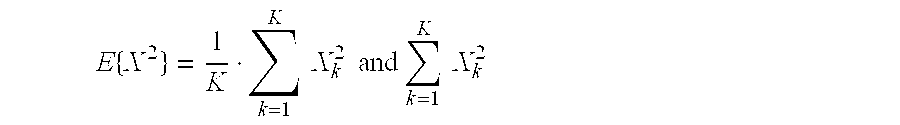
- the required size for each array is unknown when the table is set up. It is contemplated to set up a table for which each entry comprises only (in one embodiment) two items: a running sum of the observations corresponding to this table index ( ⁇ X K ), and a count of the number of observations that have been so added (K).
- an extension of the TIE tables to measure variance is contemplated. Allocating three items for each table entry, instead of two, could extend the usefulness of a TIE table. The third item can be used to hold a running sum of the squares of the observations for each table index. The variance for each table index is computed in estimating the (ISI+DCD) versus data pattern 212 , using the following equation:
- [0066] is the third item in the table.
- the completed rising-edge table and falling-edge table can be used to estimate the probability distribution function (PDF) of the ISI+DCD. It is useful to know the PDF of the ISI+DCD for the purpose of estimating the PDF of the overall jitter. Those skilled in the art will recognize that this knowledge allows the eye-opening at a given BER to be predicted (e.g., using a bathtub curve).
- PDF probability distribution function
- the estimated PDF for the ISI+DCD is formed as follows.
- each element in the tables comprises at least two pieces of information. The first piece of information is the number of times that the corresponding pattern was observed. This is the value K in equations 2 and 3. The second piece of information is the mean ISI that corresponds to that pattern, which is the value ⁇ overscore (X) ⁇ in equations 2 and 3.
- a histogram is now created using all the entries in both of the tables.
- the horizontal axis of the histogram represents the mean time interval error, in seconds or other convenient units.
- the vertical axis of the histogram represents the number of times the corresponding TIE value was observed.
- the mean ISI value ( ⁇ overscore (X) ⁇ ) is used as the horizontal coordinate into the histogram, and the number of observations (K) is accumulated with all the other populations from other table entries with the same mean ISI.
- the vertical axis may be divided (normalized) by the total number of jitter observations represented by the histogram (since this will allow the histogram to be interpreted more naturally as a PDF). It will be recognized by those skilled in the art that the actual construction of a histogram is useful conceptually but not necessary practically, and that the same information regarding the ISI+DCD PDF may be extracted using more direct techniques.
- the data pattern being analyzed can be completely arbitrary.
- the data pattern need not be a repeating pattern, and if repeating, the pattern length need not be known.
- Known methods only measure the amplitude of the total ISI jitter (i.e., the ISI jitter due to both rising and falling edges combined). The analysis that is performed according to the described methods can reveal a number of more specific details.
- the following quantities can be measured and reported: the total amplitude of the ISI jitter on a specified edge only, the two specific data patterns that account for the extrema of the ISI jitter for a specified edge, and the specific bits or bit pairs (transitions) within the analysis window that account for the greatest variability in the data dependency.
- ISI data-dependent
- jitter cannot be distinguished from periodic jitter that happens to be exactly harmonically related to the fundamental frequency of a repeating pattern.
- Separation methods of the prior art that rely on a spectral approach can make a distinction only if a spectral peak due to periodic jitter is sufficiently removed from any ISI-related peaks.
- the described approach is capable of distinguishing periodic jitter components that fall much closer to such ISI-related spectral artifacts.
- the invention has been primarily described within the context of a method of separating the jitter components on an arbitrary serial data stream utilizing a DSO. It will be appreciated by those skilled in the art and informed by the teachings of the present invention that devices other than a DSO can be used in conjunction with the present invention.
Landscapes
- Engineering & Computer Science (AREA)
- Quality & Reliability (AREA)
- Computer Networks & Wireless Communication (AREA)
- Signal Processing (AREA)
- Dc Digital Transmission (AREA)
Abstract
Description
- This application claims priority from U.S. Provisional Patent Application No. 60/422,631, filed Oct. 29, 2002 and entitled “Method for Decomposing Timing Jitter on Arbitrary Serial Data Sequences,” which is incorporated herein by reference for all purposes.
- The invention relates generally to jitter measurement and, more particularly, methods and apparatus for decomposing timing jitter on signals under test (SUTs) comprising arbitrary serial data sequences.
- As tighter timing margins and rapidly ascending clock rates drive today's high-speed designs, timing jitter (hereafter referred to simply as “jitter”) is becoming a more significant cause of system errors. Jitter can significantly reduce margin in an otherwise sound design. For example, excessive jitter can increase the bit error rate (BER) of a communications signal by incorrectly transmitting a data bit stream. In digital systems, jitter can violate timing margins, causing circuits to behave improperly. As a consequence, measuring jitter accurately is necessary to determine the robustness of a system and how close it is to failing.
- In the field of serial data communications, the term “jitter” refers to the deviation of the significant edges in a sequence of data bits from their ideal locations in time. On serial data links, the data clock is typically not transmitted with the data, so the jitter can cause data errors at the receiving end.
- Jitter can be divided into two generalized categories: deterministic jitter (DJ) and random jitter (RJ). These two categories of jitter accumulate differently in the serial data communications link, and it is desirable to be able to separate and measure each of the two categories of jitter. The deterministic jitter can further be divided into three components: inter-symbol interference (ISI), duty cycle distortion (DCD) and periodic jitter (PJ). It is again desirable to measure each individual component of the deterministic jitter as an aid in diagnosing the cause(s) of the jitter.
- A number of methods have been developed for measuring jitter on data streams, and for decomposing this jitter into its various components. Signal acquisition devices such as digital storage oscilloscopes (DSOS) can be used to facilitate real time jitter analysis of an SUT.
- A weakness of several of the known methods is that they require a repeating pattern of known length in order to separate out one of the jitter components, namely, the ISI. In one of the known methods, the data sequence must consist solely of a repeating pattern of known length, even though the specific bit values need not be known. In another prior art method, a pattern for which the data bits are completely known must be repeated (possibly interspersed with other data).
- Moreover, existing methods that provide analysis on an arbitrary data stream are not capable of fully decomposing the jitter, and require expensive, special-purpose equipment. Existing methods for fully decomposing jitter require that the data stream carry a repeating pattern with a known length, or a completely known sub-pattern that is frequently repeated.
- These and other deficiencies of the prior art are addressed by the present invention of a method and apparatus for decomposing timing jitter on arbitrary serial data sequences. Specifically, in one embodiment according to the present invention, a method is provided of decomposing timing jitter on a signal under test (SUT) comprising an arbitrary serial data stream. The method comprises performing a statistical analysis on a group of measurements, where each measurement comprises a timing jitter value and an associated bit pattern representing the bits falling within an analysis window, said window being successively located at a plurality of positions within the data stream.
- The teachings of the present invention can be readily understood by considering the following detailed description in conjunction with the accompanying drawings, in which:
- FIG. 1 depicts a high level block diagram of a signal analysis system;
- FIG. 2 depicts a flow diagram of an
analysis program 159 for separating the jitter components on a serial data stream suitable for use in the system of FIG. 1; - FIG. 3 depicts a flow diagram of the steps performed by the
analysis program 159 in estimating the ISI+DCD versus data pattern; - FIG. 4 depicts a series of bits according to an embodiment of the present invention;
- FIG. 5 depicts another series of bits according to an embodiment of the present invention; and
- FIG. 6 depicts a flow diagram of the steps performed by the
analysis program 159 in removing the ISI+DCD jitter from the serial data stream. - To facilitate understanding, identical reference numerals have been used, where possible, to designate identical elements that are common to the figures.
- The subject invention will be primarily described within the context of a measurement apparatus such as a DSO. However, it will be appreciated by those skilled in the art that the invention may be advantageously employed in any signal measurement or analysis device in which one or a plurality of SUTs may be processed to derive the timing parameters of a plurality of contiguous events.
- FIG. 1 depicts a high level block diagram of a signal analysis device. Specifically, the system (signal analysis device) 110 of FIG. 1 comprises an analog to digital (A/D)
converter 112, aclock source 130, anacquisition memory 140, acontroller 150, aninput device 160, adisplay device 170 and aninterface device 180. - The A/
D converter 112 receives and digitizes an SUT in response to a clock signal CLK produced by theclock source 130. The clock signal CLK is preferably a clock signal adapted to cause the A/D converter 112 to operate at a maximum sampling rate, though other sampling rates may be selected. Theclock source 130 is optionally responsive to a clock control signal CC produced by thecontroller 150 to change frequency and/or pulse width parameters associated with the clock signal CLK. - A digitized output signal SUT′ produced by the A/
D converter 112 is stored in theacquisition memory 140. Theacquisition memory 140 cooperates with thecontroller 150 to store the data samples provided by the A/D converter 110 in a controlled manner such that the samples from the A/D converter 110 may be provided to thecontroller 150 for further processing and/or analysis. - The
controller 150 is used to manage the various operations of thesystem 110. Thecontroller 150 performs various processing and analysis operations on the data samples stored within theacquisition memory 140. Thecontroller 150 receives user commands via aninput device 160, illustratively a keypad or pointing device. Thecontroller 150 provides image-related data to adisplay device 170, illustratively a cathode ray tube (CRT), liquid crystal display (LCD) or other display device. Thecontroller 150 optionally communicates with a communications link COMM, such as a general purpose interface bus (GPIB), Internet protocol (IP), Ethernet or other communications link via theinterface device 180. It is noted that theinterface device 180 is selected according to the particular communications network used. An embodiment of thecontroller 150 will be described in more detail below. - The
system 110 of FIG. 1 is depicted as receiving only one SUT. However, it will be appreciated by those skilled in the art that many SUTs may be received and processed by thesystem 110. Each SUT is preferably processed using a respective A/D converter 112, which respective A/D converter may be clocked using the clock signal CLK provided by a common orrespective clock source 130 or some other clock source. Each of the additional digitized SUTs is coupled to theacquisition memory 140 or additional acquisition memory (not shown). Any additional acquisition memory communicates with thecontroller 150, either directly or indirectly through an additional processing element. - The
controller 150 comprises aprocessor 154 as well asmemory 158 for storingvarious control programs 159. Theprocessor 154 cooperates withconventional support circuitry 156 such as power supplies, clock circuits, cache memory and the like, as well as circuits that assist in executing the software routines stored in thememory 158. As such, it is contemplated that some of the process steps discussed herein as software processes may be implemented within hardware, for example as circuitry that cooperates with theprocessor 154 to perform various steps. Thecontroller 150 also contains input/output (I/O)circuitry 152 that forms an interface between the various functional elements communicating with thecontroller 150. For example, in the embodiment of FIG. 1, thecontroller 150 optionally communicates with the clock source 130 (via clock control signal CC). Thecontroller 150 also communicates with theinput device 160 via a signal path IN, adisplay device 170 via a signal path OUT and theinterface device 180 via a signal path INT and theacquisition memory 140 via signal path MB. Thecontroller 150 may also communicate with additional functional elements (not shown), such as those described herein as relating to additional channels, SUT processing circuitry, switches, decimators and the like. It is noted that thememory 158 of thecontroller 150 may be included within theacquisition memory 140, that theacquisition memory 140 may be included within thememory 158 of thecontroller 150, or that a shared memory arrangement may be provided. - Although the
controller 150 is depicted as a general purpose computer that is programmed to perform various control functions in accordance with the present invention, the invention can be implemented in hardware as, for example, an application specific integrated circuit (ASIC). As such, the process steps described herein are intended to be broadly interpreted as being equivalently performed by software, hardware or a combination thereof. - Considering now a typical jitter measurement sequence, a waveform is acquired and stored in the memory of a DSO. The invention provides apparatus and methods for separating the jitter components on an arbitrary serial data stream. As mentioned herein, existing methods that provide analysis on an arbitrary data stream are not capable of fully decomposing the jitter, and are expensive. Existing methods for fully decomposing jitter require that the data stream carry a repeating pattern with a known length, or a completely known sub-pattern that is frequently repeated. In contrast, a proposed method performs a full decomposition on completely arbitrary data streams, with no requirement for repetition or for prior knowledge of the data sequence.
- In one embodiment, a methodology determined by the inventor relies on an assumption that each data transition's significant causative effects on other transitions are contained within a relatively small “time window” surrounding that transition. For example, a specific transition may only have a measurable effect on transitions that occur in the four or five symbols that immediately follow it.
- For example, consider two adjacent bits at an arbitrary location in the data stream. The four possible data patterns that may be represented by the two bits are: {0 to 0, 0 to 1, 1 to 0, 1 to 1}. Of these, the first and last patterns do not have a transition, and thus are not subject to jitter. In one embodiment, only when a pair of bits of alternate value occurs do we need to look for jitter. Furthermore, since systems frequently exhibit one impulse response for rising edges and a different impulse response for falling edges, the 0 to 1 transition should be analyzed separately from the 1 to 0 transition. For illustrative purposes, the rising (0 to 1) transition will be described herein.
- For illustrative purposes, assume that data-dependent jitter (ISI or DDJ) is caused solely by the effect mentioned above, and that the step response only differs from its steady-state value over a time period corresponding to some small number of bits, N. Then, the number of different patterns that need to be considered (even if the composite data stream has random and/or non-repeating content) is limited to (on the order of) 2 N.
- For example, assume that a rising edge may be affected by the four bits that preceded the 0 to 1 pattern, and by the single subsequent bit. Since only five bits (in addition to the two bits that define the transition) are to be considered in this example, there are 2 5 cases. (There are another 25 cases for the falling edge, but those can be considered separately).
- FIG. 2 depicts a flow diagram of a
method 200 suitable for use in thesystem 110 of FIG. 1. Specifically, FIG. 2 depicts a method of separating the jitter components on a serial data stream, even if the data pattern is not known or repeating. In one embodiment according to the present invention, this method comprises measuring the Time Interval Errors (TIE) on thedata stream 210, estimating (finding) the (ISI+DCD) versusdata pattern 212, calculating the DCD and the peak-to-peakISI 214, removing (subtracting out) the (ISI+DCD) from theTIE record 216 and using a spectral approach to separate the remaining TIE into periodic andrandom components 218. It is envisioned by the inventor that in some embodiments approaches other than a spectral approach can be implemented (e.g., a histogram-based approach). - The exemplary methodology of FIG. 2 will now be examined in more detail. At
step 210, when measuring the Time Interval Errors (TIE) on the data stream, thesystem 110 captures and analyzes a sample of the SUT. The SUT has continuous amplitude-versus-time record of some finite duration. Thesystem 110 captures and analyzes the SUT so that the result of the analysis is an ordered list of time tags, where each time tag represents the exact time when the data-bearing signal crossed a chosen threshold. - The
system 110 also generates an array representing the actual binary data bits comprising the signal. This process is accomplished, for example, using a DSO for the data capture, and a digital computer equipped with the appropriate filtering and interpolating software for the analysis. - The
system 110 compares the acquired list of time tags to a list of time tags representing a jitter-free version of the same data stream that was acquired. The jitter-free version of the data stream is generated by one of several methods, generally falling under the topic of Clock Recovery, known to those of ordinary skill in the art. The result of this comparison is an ordered list of time-interval error tags, which is referred to herein as a “TIE record.” At each point where no transition occurs (because two adjacent bits are identical), a value of zero, or any other convenient value, may be inserted as a place-holder. These values will be replaced when separating the remaining TIE into periodic andrandom components 218. - At
step 212, in reference to estimating the (ISI+DCD) versus data pattern, a table of 2N arrays is allocated in a suitable memory space. Here, N is the number of bits (in addition to the two bits comprising the data transition) that are considered to significantly contribute to the data-dependent jitter. FIG. 3 will show an exemplary flow diagram of amethod 300 suitable for compiling tables of ISI and DCD values. - Referring to FIG. 3, in this illustrative example, N is chosen to be equal to 5 at
step 320 since it is desired to consider four bits preceding the transition and one bit following the transition. Thus, for each unique pattern of N bits that surround a transition, there exists in this “rising-edge” table an array that may be used to store information relevant to that unique pattern. (A similar table is prepared to support falling-edge analysis.) Atstep 321, the table of arrays is allocated as mentioned herein. - At
step 322, an analysis window with a width of N+2 bits is positioned on the first N+2 bits in the serial data array. During an iterative sequence of analysis cycles (steps 323-328), the analysis window is slid along the list of binary data bits, from beginning to end. After each analysis cycle, the window is advanced by one bit (step 328). This process is suggested graphically in FIG. 4, using N+2=7. - During each analysis cycle, the
system 110 performs a number of operations on the bits in the current analysis window. For illustrative purposes, the bits can be identified as shown in FIG. 5. The bits tα and tβ represent the bit positions that thesystem 110 is analyzing (and that may or may not contain a transition). The bits p1-pj are the i bits preceding the transition, which are considered to contribute to the DDJ. The bits s1-sj are the j bits subsequent to the transition that are considered to contribute to the DDJ. In this illustrative example, i=4 and j=1 so that N=i+j=5. - In one embodiment, the operations for each cycle are as follows. If the transition bits (t α, tβ) are (0, 0) or (1, 1), then there is no transition corresponding to this analysis cycle. In other words, there was no positive edge transition at
step 323 and no negative edge transition atstep 325. In the absence of transitions then the pattern-matching operation (described infra) is skipped for this processing cycle. - At
step 327, if there are more bits in the TIE array then the analysis window is simply advanced by one bit atstep 328. - At
step 323, the transition bits (tα, tβ) are checked for a (0, 1) pattern, corresponding to a rising transition. If a rising transition is found then a rising-edge analysis (step 324) is performed according to the pattern-matching operation and the observations are added to the rising-edge table. - At
step 325, the transition bits (tα, tβ) are checked for a (1,0) pattern, corresponding to a falling transition. If a falling transition is found then a falling-edge analysis (step 326) is performed in a manner analogous to the pattern-matching operation but using a separate “falling-edge” table, and the observations are added to the falling-edge table. - Regarding the pattern-matching operation, the {p i} bits and {sj} bits are concatenated into a single N-bit digital word, which is used as an index into the “rising-edge” table. The
system 110 adds the time-interval-error quantity that corresponds to the bit pair (tα, tβ) to the array at this table index. Thesystem 110 later performs a statistical analysis on the elements of this array atstep 329. - It will be appreciated by those skilled in the art that the concatenation method used in the pattern-matching operation is one illustrative method of uniquely mapping the possible bit patterns to entries in the “rising-edge” table. Any other method that establishes a one-to-one mapping between bit patterns and table entries may be used to implement the pattern-matching operation.
- After the
system 110 slides the analysis window over the full length of the available data, each (in one embodiment) element of the table related to the discussion of FIG. 4 comprises an array including the observations of the jitter error corresponding to a particular bit pattern surrounding a rising edge. At this point, for each of the 2N elements in the rising edge table, thesystem 110 calculates the mean value of the array of jitter observations for that element. Since the table only (in one embodiment) includes observations related to rising edges, there will be no duty-cycle-related jitter in the observations in one embodiment. If there is no random or periodic jitter on the signal, and if a sufficient number of preceding bits (i) and succeeding bits (j) have been included in the analysis, all (in one embodiment) of the observations in a given table position should be identical and should represent the amount of ISI caused by the corresponding bit pattern. In this case, the mean value of the observations will be equal to each of the identical observations. If the random jitter and/or periodic jitter is non-zero and is not correlated with the data sequence, then the mean value of the observations in each table element is a valid estimate of the jitter caused by the corresponding bit pattern. The quality of this estimate grows as the number of observations being averaged grows. - The most positive mean value in the rising-edge table (referred to herein as ISI+ max ) indicates the peak forward deviation (that is, advanced in time) among the rising edges. The most negative mean value (referred to herein as ISI+ min ) indicates the peak reverse deviation (that is, retarded in time) among the rising edges. The difference between these two numbers is the peak-to-peak deviation due to ISI on rising edges. Similarly, a falling-edge analysis will reveal ISI− max and ISI− min , the peak ISI deviations on falling edges. Finally, the difference between MAX{ISI+ max , ISI− max } and MIN{ISI+ min , ISI− min } gives the peak-to-peak value of ISI+DCD. A separate computation of DCDpk-pk, described herein, allows the
system 110 to determine the value of ISIpk-pk by subtraction. - Referring again to step 214 of calculating the DCD and peak-to-peak ISI of FIG. 2, the
system 110 can estimate the duty-cycle distortion (DCD) in a separate operation as follows. - The
system 110 forms a weighted average of the mean rising-edge ISI values from the rising-edge table thesystem 110 constructed. That is, thesystem 110 multiplies the mean ISI value corresponding to each (in one embodiment) data pattern by the number of times thesystem 110 observed that pattern. Thesystem 110 adds these products together for the patterns, and divides the sum by the number of pattern-matching operations. The result of this calculation is the mean ISI for all rising edges, ISI+ mean . Thesystem 110 repeats this calculation on the falling-edge table to compute the mean falling-edge ISI, ISI− mean . The difference between these two means is the jitter related to duty cycle, or DCD. - It is noteworthy that the
system 110 can also determine the values ISI+ mean and ISI− mean by going back to the original TIE record and computing the mean TIE on the rising edges and the mean TIE on the falling edges, respectively. - This DCD is a peak-to-peak value (since the probability density function for DCD comprises of a pair of impulses). The (ISI+DCD) the
system 110 calculated herein was also a peak-to-peak value. Therefore, thesystem 110 calculates the peak-to-peak ISI by: - ISI pk-pk=(ISI+DCD)−DCD Eq. 1
- Referring again to step 216 of subtracting out the (ISI+DCD) from the TIE record, one result of finding (ISI+DCD) versus the data pattern was a table that provided the (ISI+DCD) value for the localized data patterns that occur in the data sequence. The
system 110 subtracts these values from the TIE record so that only the periodic and random components of the TIE remain. - In a manner similar to the operations discussed with respect to FIG. 4, the
system 110 slides an analysis window with a width of N+2 bits along the list of binary data bits, from beginning to end. A jitter-removal operation is performed for each window position, after which thesystem 110 advances the window by one bit. FIG. 6 will show a flow diagram of amethod 600 suitable for removing ISI and DCD from an SUT. - More specifically, referring to FIGS. 5 and 6, during the ISI+DCD removal process the
system 110 performs the following operations. In one embodiment, atstep 630 thesystem 110 places an analysis window of length N+2 on the first N+2 bits of the TIE array. Atstep 631, the transition bits (tα, tβ) are checked for a (0, 1) pattern, corresponding to a rising transition. If a rising transition is found then thesystem 110 selects the rising-edge table atstep 632 and applies the jitter-correction operation (described infra). Atstep 633, the transition bits (tα, tβ) are checked for a (1,0) pattern, corresponding to a falling transition. If a falling transition is found, then thesystem 110 selects the falling-edge table atstep 634 and applies the jitter-correction operation. If, on a given processing cycle, the transition bits (tα, tβ) comprise (0, 0) or (1, 1), then there is no transition on this cycle and neither step 632 nor 634 is performed. - At
step 635, if there are no more bits in the TIE array then the ISI+DCD removal process 216 is complete. If there are more bits in the TIE array then thesystem 110 advances the analysis window by one bit atstep 636 and begins the next processing cycle atstep 631. - The aforementioned jitter-correction operation is described as follows. The
system 110 concatenates the {pi} bits and {sj} bits into an N-bit digital word. Thesystem 110 uses the word as an index into the table selected in the prior operation. Thesystem 110 subtracts the ISI value indexed by these bits (i.e., the jitter that is attributed to this pattern) from the value in the TIE array that corresponds to the (tα, tβ) transition. - Referring again to separating the remaining TIE into periodic and
random components 218, thesystem 110 has compensated the TIE record that now remains so that the TIE record no longer includes the effect of ISI or DCD. Thesystem 110 may separate the TIE record into periodic and random components using substantially the same technique described herein, based on spectral analysis. In one embodiment, thesystem 110 treats all spectral impulses as periodic jitter. - At each point in the compensated TIE record where no corresponding transition occurred because two adjacent bits are identical, e.g. (0,0) or (1, 1), the
system 110 inserts an estimated TIE value by linear interpolation from the nearest two bounding TIE values derived from actual transitions. Thesystem 110 converts the interpolated TIE record to the complex frequency domain by applying a processing window (e.g., Blackman, etc.) and then performing a Fast-Fourier Transform (FFT). - The system forms an estimate of the power spectral density by representing the FFT results as magnitude versus frequency. The
system 110 determines the locations (or bins) in the power spectrum corresponding to deterministic noise (i.e., periodic jitter) by applying techniques known to those of skill in the art. - Beginning with the complex FFT results from above, the
system 110 sets the bins attributable to random noise to zero so that only the bins representing deterministic noise remain. Thesystem 110 converts this array back to the time domain via an inverse FFT, after which the effects of the processing window are reversed over the central third of the record. Disregarding those positions corresponding to TIE values that were interpolated, the peak-to-peak value of this periodic jitter is found. - Beginning with the complex FFT results, the
system 110 calculates the RMS value of the bins attributable to noise. Since this calculation is based on a subset of the total number of bins, it is normalized by the number of bins used in the calculation. The resulting RMS value is taken as the standard deviation of the random jitter, which is assumed to have a Gaussian probability density function. - In various embodiments, estimating the (ISI+DCD) versus data pattern 212 (among other operations) is modified. In the embodiment described supra, a table of 2N entries is allocated, where each entry can hold an array of TIE observations. After the table has been filled, the
system 110 computes the mean value of the observations in the arrays (after which the individual observations are not needed). However, in this embodiment the required size for each array is unknown when the table is set up. It is contemplated to set up a table for which each entry comprises only (in one embodiment) two items: a running sum of the observations corresponding to this table index (□XK), and a count of the number of observations that have been so added (K). Thesystem 110 can calculate the mean for each table entry using the formula:
- where K and

- are the two items in the table.
- In another embodiment, an extension of the TIE tables to measure variance is contemplated. Allocating three items for each table entry, instead of two, could extend the usefulness of a TIE table. The third item can be used to hold a running sum of the squares of the observations for each table index. The variance for each table index is computed in estimating the (ISI+DCD) versus
data pattern 212, using the following equation: - Var(X)=E{(X−{overscore (X)}) 2 }=E{X 2}−({overscore (X)}) 2 Eq. 3
- where
- is the third item in the table.
- In another embodiment, the completed rising-edge table and falling-edge table can be used to estimate the probability distribution function (PDF) of the ISI+DCD. It is useful to know the PDF of the ISI+DCD for the purpose of estimating the PDF of the overall jitter. Those skilled in the art will recognize that this knowledge allows the eye-opening at a given BER to be predicted (e.g., using a bathtub curve). The estimated PDF for the ISI+DCD is formed as follows. In one embodiment, each element in the tables comprises at least two pieces of information. The first piece of information is the number of times that the corresponding pattern was observed. This is the value K in
equations equations - A histogram is now created using all the entries in both of the tables. The horizontal axis of the histogram represents the mean time interval error, in seconds or other convenient units. The vertical axis of the histogram represents the number of times the corresponding TIE value was observed. For each element in the tables, the mean ISI value ({overscore (X)}) is used as the horizontal coordinate into the histogram, and the number of observations (K) is accumulated with all the other populations from other table entries with the same mean ISI. Once all the table entries have been accumulated into the histogram, the vertical axis may be divided (normalized) by the total number of jitter observations represented by the histogram (since this will allow the histogram to be interpreted more naturally as a PDF). It will be recognized by those skilled in the art that the actual construction of a histogram is useful conceptually but not necessary practically, and that the same information regarding the ISI+DCD PDF may be extracted using more direct techniques.
- Thus, a method of separating the jitter components on an arbitrary serial data stream has been shown and described. The data pattern being analyzed can be completely arbitrary. As mentioned herein, the data pattern need not be a repeating pattern, and if repeating, the pattern length need not be known. Known methods only measure the amplitude of the total ISI jitter (i.e., the ISI jitter due to both rising and falling edges combined). The analysis that is performed according to the described methods can reveal a number of more specific details. For each of the two edges (rising and falling), the following quantities can be measured and reported: the total amplitude of the ISI jitter on a specified edge only, the two specific data patterns that account for the extrema of the ISI jitter for a specified edge, and the specific bits or bit pairs (transitions) within the analysis window that account for the greatest variability in the data dependency.
- In the prior art, data-dependent (ISI) jitter cannot be distinguished from periodic jitter that happens to be exactly harmonically related to the fundamental frequency of a repeating pattern. Separation methods of the prior art that rely on a spectral approach can make a distinction only if a spectral peak due to periodic jitter is sufficiently removed from any ISI-related peaks. The described approach is capable of distinguishing periodic jitter components that fall much closer to such ISI-related spectral artifacts.
- The invention has been primarily described within the context of a method of separating the jitter components on an arbitrary serial data stream utilizing a DSO. It will be appreciated by those skilled in the art and informed by the teachings of the present invention that devices other than a DSO can be used in conjunction with the present invention.
- While the foregoing is directed to the preferred embodiment of the present invention, other and further embodiments of the invention may be devised without departing from the basic scope thereof, and the scope thereof is determined by the claims that follow.
Claims (20)
Priority Applications (1)
| Application Number | Priority Date | Filing Date | Title |
|---|---|---|---|
| US10/625,951 US7254168B2 (en) | 2002-10-29 | 2003-07-23 | Method for decomposing timing jitter on arbitrary serial data sequences |
Applications Claiming Priority (2)
| Application Number | Priority Date | Filing Date | Title |
|---|---|---|---|
| US42263102P | 2002-10-29 | 2002-10-29 | |
| US10/625,951 US7254168B2 (en) | 2002-10-29 | 2003-07-23 | Method for decomposing timing jitter on arbitrary serial data sequences |
Publications (2)
| Publication Number | Publication Date |
|---|---|
| US20040136450A1 true US20040136450A1 (en) | 2004-07-15 |
| US7254168B2 US7254168B2 (en) | 2007-08-07 |
Family
ID=32717471
Family Applications (1)
| Application Number | Title | Priority Date | Filing Date |
|---|---|---|---|
| US10/625,951 Active 2025-09-27 US7254168B2 (en) | 2002-10-29 | 2003-07-23 | Method for decomposing timing jitter on arbitrary serial data sequences |
Country Status (1)
| Country | Link |
|---|---|
| US (1) | US7254168B2 (en) |
Cited By (17)
| Publication number | Priority date | Publication date | Assignee | Title |
|---|---|---|---|---|
| US20030115017A1 (en) * | 2001-12-14 | 2003-06-19 | Jie Sun | Method and apparatus for analyzing a disribution |
| US20050080574A1 (en) * | 2003-10-14 | 2005-04-14 | Draving Steven D. | Method and apparatus for decomposing signal jitter using multiple acquisitions |
| US20050107981A1 (en) * | 2003-11-14 | 2005-05-19 | The Boeing Company | Window average statistics model for pointing stability jitter analysis |
| US20050286627A1 (en) * | 2004-06-28 | 2005-12-29 | Guide Technology | System and method of obtaining random jitter estimates from measured signal data |
| US20060120444A1 (en) * | 2004-11-08 | 2006-06-08 | Sassan Tabatabaei | Data-dependent jitter (DDJ) calibration methodology |
| US20060132116A1 (en) * | 2004-08-09 | 2006-06-22 | Hamre John D | Waveform analyzer |
| US20070264299A1 (en) * | 2003-01-28 | 2007-11-15 | Hughes Kenneth A | Cyano anthranilamide insecticides |
| US20070274378A1 (en) * | 2006-05-26 | 2007-11-29 | Texas Instruments, Inc. | Estimation of BER performance |
| US7388937B1 (en) * | 2003-04-21 | 2008-06-17 | Pmc-Sierra, Inc. | Systems and methods for jitter analysis of digital signals |
| US20090063111A1 (en) * | 2007-08-30 | 2009-03-05 | Micron Technology, Inc. | Jittery signal generation with discrete-time filtering |
| WO2009040060A1 (en) * | 2007-09-21 | 2009-04-02 | Rohde & Schwarz Gmbh & Co. Kg | Method and device for recording jitter data |
| US20090132207A1 (en) * | 2007-11-07 | 2009-05-21 | Guidetech, Inc. | Fast Low Frequency Jitter Rejection Methodology |
| US20110040509A1 (en) * | 2007-12-14 | 2011-02-17 | Guide Technology, Inc. | High Resolution Time Interpolator |
| US7941287B2 (en) | 2004-12-08 | 2011-05-10 | Sassan Tabatabaei | Periodic jitter (PJ) measurement methodology |
| US20110292987A1 (en) * | 2010-05-27 | 2011-12-01 | Tektronix, Inc. | Method for decomposing and analyzing jitter using spectral analysis and time-domain probability density |
| CN111474408A (en) * | 2019-01-23 | 2020-07-31 | 罗德施瓦兹两合股份有限公司 | Jitter determination method and measuring instrument |
| US11121783B2 (en) * | 2019-01-23 | 2021-09-14 | Rohde & Schwarz Gmbh & Co. Kg | Jitter determination method and measurement instrument |
Families Citing this family (11)
| Publication number | Priority date | Publication date | Assignee | Title |
|---|---|---|---|---|
| US7460591B2 (en) * | 2004-08-30 | 2008-12-02 | Agilent Technologies, Inc. | Method and apparatus using re-sampled tie records to characterize jitter in a digital signal |
| US7480329B2 (en) * | 2004-10-29 | 2009-01-20 | Agilent Technologies, Inc. | Method of finding data dependent timing and voltage jitter for different bits in an arbitrary digital signal in accordance with selected surrounding bits |
| US7480355B2 (en) * | 2005-02-16 | 2009-01-20 | Agilent Technologies, Inc. | Method for equalizing a digital signal through removal of data dependent jitter |
| US7460592B2 (en) * | 2005-05-04 | 2008-12-02 | Advantest Corporation | Apparatus for measuring jitter and method of measuring jitter |
| US20070285081A1 (en) * | 2006-05-16 | 2007-12-13 | Carole James A | Method and system for statistical measurement and processing of a repetitive signal |
| US8452560B2 (en) * | 2006-12-29 | 2013-05-28 | Teradyne, Inc. | Identifying periodic jitter in a signal |
| US8327196B2 (en) * | 2008-07-16 | 2012-12-04 | International Business Machines Corporation | Identifying an optimized test bit pattern for analyzing electrical communications channel topologies |
| US8000931B2 (en) * | 2008-10-23 | 2011-08-16 | Advantest Corporation | Deterministic component model judging apparatus, judging method, program, recording medium, test system and electronic device |
| US8473233B1 (en) | 2009-08-05 | 2013-06-25 | Gary K. Giust | Analyzing jitter in a clock timing signal |
| US9003549B2 (en) | 2010-08-31 | 2015-04-07 | Gary K. Giust | Analysis of an analog property of a signal |
| US8891602B1 (en) | 2011-05-19 | 2014-11-18 | Gary K. Giust | Analyzing jitter with noise from the measurement environment |
Citations (9)
| Publication number | Priority date | Publication date | Assignee | Title |
|---|---|---|---|---|
| US6137283A (en) * | 1995-02-22 | 2000-10-24 | Michael K. Williams | Process and machine for signal waveform analysis |
| US20030031284A1 (en) * | 2001-03-20 | 2003-02-13 | Masahiro Ishida | Probability estimating apparatus and method for peak-to-peak clock skews |
| US20040062301A1 (en) * | 2002-09-30 | 2004-04-01 | Takahiro Yamaguchi | Jitter measurement apparatus and jitter measurement method |
| US6753677B1 (en) * | 2003-02-28 | 2004-06-22 | Agilent Technologies, Inc. | Trigger jitter reduction for an internally triggered real time digital oscilloscope |
| US20040146097A1 (en) * | 2003-01-29 | 2004-07-29 | Jungerman Roger Lee | Characterizing jitter of repetitive patterns |
| US6832172B2 (en) * | 2001-06-15 | 2004-12-14 | Tektronix, Inc. | Apparatus and method for spectrum analysis-based serial data jitter measurement |
| US20040260492A1 (en) * | 2003-06-19 | 2004-12-23 | Francine Halle | Direct jitter analysis of binary sampled data |
| US6898535B2 (en) * | 2003-10-14 | 2005-05-24 | Agilent Technologies, Inc. | Method and apparatus for decomposing signal jitter using multiple acquisitions |
| US6993695B2 (en) * | 2001-06-06 | 2006-01-31 | Agilent Technologies, Inc. | Method and apparatus for testing digital devices using transition timestamps |
-
2003
- 2003-07-23 US US10/625,951 patent/US7254168B2/en active Active
Patent Citations (9)
| Publication number | Priority date | Publication date | Assignee | Title |
|---|---|---|---|---|
| US6137283A (en) * | 1995-02-22 | 2000-10-24 | Michael K. Williams | Process and machine for signal waveform analysis |
| US20030031284A1 (en) * | 2001-03-20 | 2003-02-13 | Masahiro Ishida | Probability estimating apparatus and method for peak-to-peak clock skews |
| US6993695B2 (en) * | 2001-06-06 | 2006-01-31 | Agilent Technologies, Inc. | Method and apparatus for testing digital devices using transition timestamps |
| US6832172B2 (en) * | 2001-06-15 | 2004-12-14 | Tektronix, Inc. | Apparatus and method for spectrum analysis-based serial data jitter measurement |
| US20040062301A1 (en) * | 2002-09-30 | 2004-04-01 | Takahiro Yamaguchi | Jitter measurement apparatus and jitter measurement method |
| US20040146097A1 (en) * | 2003-01-29 | 2004-07-29 | Jungerman Roger Lee | Characterizing jitter of repetitive patterns |
| US6753677B1 (en) * | 2003-02-28 | 2004-06-22 | Agilent Technologies, Inc. | Trigger jitter reduction for an internally triggered real time digital oscilloscope |
| US20040260492A1 (en) * | 2003-06-19 | 2004-12-23 | Francine Halle | Direct jitter analysis of binary sampled data |
| US6898535B2 (en) * | 2003-10-14 | 2005-05-24 | Agilent Technologies, Inc. | Method and apparatus for decomposing signal jitter using multiple acquisitions |
Cited By (32)
| Publication number | Priority date | Publication date | Assignee | Title |
|---|---|---|---|---|
| US7016805B2 (en) * | 2001-12-14 | 2006-03-21 | Wavecrest Corporation | Method and apparatus for analyzing a distribution |
| US20030115017A1 (en) * | 2001-12-14 | 2003-06-19 | Jie Sun | Method and apparatus for analyzing a disribution |
| US20070264299A1 (en) * | 2003-01-28 | 2007-11-15 | Hughes Kenneth A | Cyano anthranilamide insecticides |
| US7388937B1 (en) * | 2003-04-21 | 2008-06-17 | Pmc-Sierra, Inc. | Systems and methods for jitter analysis of digital signals |
| US20050080574A1 (en) * | 2003-10-14 | 2005-04-14 | Draving Steven D. | Method and apparatus for decomposing signal jitter using multiple acquisitions |
| US6898535B2 (en) * | 2003-10-14 | 2005-05-24 | Agilent Technologies, Inc. | Method and apparatus for decomposing signal jitter using multiple acquisitions |
| US6988051B2 (en) * | 2003-11-14 | 2006-01-17 | The Boeing Company | Window average statistics model for pointing stability jitter analysis |
| US20050107981A1 (en) * | 2003-11-14 | 2005-05-19 | The Boeing Company | Window average statistics model for pointing stability jitter analysis |
| US20050286627A1 (en) * | 2004-06-28 | 2005-12-29 | Guide Technology | System and method of obtaining random jitter estimates from measured signal data |
| US7512196B2 (en) * | 2004-06-28 | 2009-03-31 | Guidetech, Inc. | System and method of obtaining random jitter estimates from measured signal data |
| US8054907B2 (en) * | 2004-08-09 | 2011-11-08 | John David Hamre | Waveform analyzer |
| US20060132116A1 (en) * | 2004-08-09 | 2006-06-22 | Hamre John D | Waveform analyzer |
| US20060120444A1 (en) * | 2004-11-08 | 2006-06-08 | Sassan Tabatabaei | Data-dependent jitter (DDJ) calibration methodology |
| US7164999B2 (en) * | 2004-11-08 | 2007-01-16 | Guide Technology, Inc. | Data-dependent jitter (DDJ) calibration methodology |
| US7941287B2 (en) | 2004-12-08 | 2011-05-10 | Sassan Tabatabaei | Periodic jitter (PJ) measurement methodology |
| US20070274378A1 (en) * | 2006-05-26 | 2007-11-29 | Texas Instruments, Inc. | Estimation of BER performance |
| US7801204B2 (en) * | 2006-05-26 | 2010-09-21 | Texas Instruments Incorporated | Estimation of BER performance |
| US20090063111A1 (en) * | 2007-08-30 | 2009-03-05 | Micron Technology, Inc. | Jittery signal generation with discrete-time filtering |
| US7953579B2 (en) * | 2007-08-30 | 2011-05-31 | Micron Technology, Inc. | Jittery signal generation with discrete-time filtering |
| WO2009040060A1 (en) * | 2007-09-21 | 2009-04-02 | Rohde & Schwarz Gmbh & Co. Kg | Method and device for recording jitter data |
| US20100141308A1 (en) * | 2007-09-21 | 2010-06-10 | Rohde & Schwarz Gmbh & Co. Kg | Method and device for clock-data recovery |
| US8208594B2 (en) | 2007-09-21 | 2012-06-26 | Rohde & Schwarz Gmbh & Co. Kg | Method and device for clock-data recovery |
| US20090132207A1 (en) * | 2007-11-07 | 2009-05-21 | Guidetech, Inc. | Fast Low Frequency Jitter Rejection Methodology |
| US8255188B2 (en) | 2007-11-07 | 2012-08-28 | Guidetech, Inc. | Fast low frequency jitter rejection methodology |
| US8064293B2 (en) | 2007-12-14 | 2011-11-22 | Sassan Tabatabaei | High resolution time interpolator |
| US20110040509A1 (en) * | 2007-12-14 | 2011-02-17 | Guide Technology, Inc. | High Resolution Time Interpolator |
| US20110292987A1 (en) * | 2010-05-27 | 2011-12-01 | Tektronix, Inc. | Method for decomposing and analyzing jitter using spectral analysis and time-domain probability density |
| CN102288840A (en) * | 2010-05-27 | 2011-12-21 | 特克特朗尼克公司 | Method for decomposing and analyzing jitter using spectral analysis and time domain probability density |
| US8594169B2 (en) * | 2010-05-27 | 2013-11-26 | Tektronix, Inc. | Method for decomposing and analyzing jitter using spectral analysis and time-domain probability density |
| CN111474408A (en) * | 2019-01-23 | 2020-07-31 | 罗德施瓦兹两合股份有限公司 | Jitter determination method and measuring instrument |
| US11121783B2 (en) * | 2019-01-23 | 2021-09-14 | Rohde & Schwarz Gmbh & Co. Kg | Jitter determination method and measurement instrument |
| US11184268B2 (en) * | 2019-01-23 | 2021-11-23 | Rohde & Schwarz Gmbh & Co. Kg | Jitter determination method and measurement instrument |
Also Published As
| Publication number | Publication date |
|---|---|
| US7254168B2 (en) | 2007-08-07 |
Similar Documents
| Publication | Publication Date | Title |
|---|---|---|
| US7254168B2 (en) | Method for decomposing timing jitter on arbitrary serial data sequences | |
| JP4204806B2 (en) | Jitter measurement method | |
| JP3696886B2 (en) | A system for measuring jitter in non-binary digital signals. | |
| US7516030B2 (en) | Measuring components of jitter | |
| US6898535B2 (en) | Method and apparatus for decomposing signal jitter using multiple acquisitions | |
| US7467336B2 (en) | Method and apparatus to measure and display data dependent eye diagrams | |
| US7388937B1 (en) | Systems and methods for jitter analysis of digital signals | |
| US7623977B2 (en) | Periodic jitter (PJ) measurement methodology | |
| US9506951B2 (en) | Method and apparatus for data acquisition with waveform trigger | |
| US20030115017A1 (en) | Method and apparatus for analyzing a disribution | |
| US20080147340A1 (en) | Method and system for measuring signal characteristics of data signals transmitted between integrated circuit chips | |
| EP2390789A1 (en) | Method for decomposing and analyzing jitter using spectral analysis and time domain probability density | |
| US9442136B2 (en) | Real-time oscilloscope for generating a fast real-time eye diagram | |
| US7668235B2 (en) | Jitter measurement algorithm using locally in-order strobes | |
| EP2985610A1 (en) | Method for determining a correlated waveform on a real time oscilloscope | |
| US7310392B2 (en) | Method and apparatus for determining inter-symbol interference for estimating data dependent jitter | |
| US8024142B1 (en) | Method and system for analyzing signal waveforms | |
| US20050232345A1 (en) | Histograms, trends and spectrums of random and deterministic jitter | |
| US20040131113A1 (en) | Zero crossing method of symbol rate and timing estimation | |
| JP2006276019A (en) | Separation of random components and deterministic components of jitters | |
| JPH06237231A (en) | Waveform discriminating device | |
| US20070250279A1 (en) | Digital data signal analysis by evaluating sampled values in conjunction with signal bit values | |
| Nilsen | Conditional averaging of overlapping pulses | |
| US11346884B2 (en) | Signal analysis method and measurement instrument | |
| US20150102799A1 (en) | Jitter determination of noisy electrical signals |
Legal Events
| Date | Code | Title | Description |
|---|---|---|---|
| AS | Assignment |
Owner name: TEKTRONIX, INC., OREGON Free format text: ASSIGNMENT OF ASSIGNORS INTEREST;ASSIGNOR:GUENTHER, MARK L.;REEL/FRAME:019481/0978 Effective date: 20030723 |
|
| STCF | Information on status: patent grant |
Free format text: PATENTED CASE |
|
| FEPP | Fee payment procedure |
Free format text: PAYOR NUMBER ASSIGNED (ORIGINAL EVENT CODE: ASPN); ENTITY STATUS OF PATENT OWNER: LARGE ENTITY |
|
| FPAY | Fee payment |
Year of fee payment: 4 |
|
| FPAY | Fee payment |
Year of fee payment: 8 |
|
| MAFP | Maintenance fee payment |
Free format text: PAYMENT OF MAINTENANCE FEE, 12TH YEAR, LARGE ENTITY (ORIGINAL EVENT CODE: M1553); ENTITY STATUS OF PATENT OWNER: LARGE ENTITY Year of fee payment: 12 |