US20030033876A1 - Apparatus and method for ultrasensitive nanoelectromechanical mass detection - Google Patents
Apparatus and method for ultrasensitive nanoelectromechanical mass detection Download PDFInfo
- Publication number
- US20030033876A1 US20030033876A1 US10/138,538 US13853802A US2003033876A1 US 20030033876 A1 US20030033876 A1 US 20030033876A1 US 13853802 A US13853802 A US 13853802A US 2003033876 A1 US2003033876 A1 US 2003033876A1
- Authority
- US
- United States
- Prior art keywords
- mass
- resonator
- nanoelectromechanical
- vibrating element
- nanoelectromechanical resonator
- Prior art date
- Legal status (The legal status is an assumption and is not a legal conclusion. Google has not performed a legal analysis and makes no representation as to the accuracy of the status listed.)
- Granted
Links
Images


Classifications
-
- G—PHYSICS
- G01—MEASURING; TESTING
- G01N—INVESTIGATING OR ANALYSING MATERIALS BY DETERMINING THEIR CHEMICAL OR PHYSICAL PROPERTIES
- G01N29/00—Investigating or analysing materials by the use of ultrasonic, sonic or infrasonic waves; Visualisation of the interior of objects by transmitting ultrasonic or sonic waves through the object
- G01N29/02—Analysing fluids
- G01N29/036—Analysing fluids by measuring frequency or resonance of acoustic waves
-
- G—PHYSICS
- G01—MEASURING; TESTING
- G01G—WEIGHING
- G01G3/00—Weighing apparatus characterised by the use of elastically-deformable members, e.g. spring balances
- G01G3/12—Weighing apparatus characterised by the use of elastically-deformable members, e.g. spring balances wherein the weighing element is in the form of a solid body stressed by pressure or tension during weighing
- G01G3/16—Weighing apparatus characterised by the use of elastically-deformable members, e.g. spring balances wherein the weighing element is in the form of a solid body stressed by pressure or tension during weighing measuring variations of frequency of oscillations of the body
-
- H—ELECTRICITY
- H01—ELECTRIC ELEMENTS
- H01J—ELECTRIC DISCHARGE TUBES OR DISCHARGE LAMPS
- H01J49/00—Particle spectrometers or separator tubes
- H01J49/26—Mass spectrometers or separator tubes
-
- G—PHYSICS
- G01—MEASURING; TESTING
- G01N—INVESTIGATING OR ANALYSING MATERIALS BY DETERMINING THEIR CHEMICAL OR PHYSICAL PROPERTIES
- G01N2291/00—Indexing codes associated with group G01N29/00
- G01N2291/02—Indexing codes associated with the analysed material
- G01N2291/025—Change of phase or condition
- G01N2291/0256—Adsorption, desorption, surface mass change, e.g. on biosensors
Definitions
- the invention relates to the application of the techniques of nanoelectromechanical systems (NEMS) to ultrasensitive mass detection.
- NEMS nanoelectromechanical systems
- Micro-Electro-Mechanical Systems is the integration of mechanical elements, sensors, actuators, and electronics on a common silicon substrate through the utilization of microfabrication technology. While the electronics are fabricated using integrated circuit (IC) process sequences (e.g., CMOS, Bipolar, or BICMOS processes), the micromechanical components are fabricated using compatible “micromachining” processes that selectively etch away parts of the silicon wafer or add new structural layers to form the mechanical and electromechanical devices.
- IC integrated circuit
- MEMS promises to revolutionize nearly every product category by bringing together silicon-based microelectronics with micromachining technology, thereby, making possible the realization of complete systems-on-a-chip. MEMS technology makes possible the integration of microelectronics with active perception and control functions, thereby, expanding the design and application space.
- NEMS nanoelectromechanical systems
- the invention is defined as a method for measuring microscopic magnitudes of mass and an apparatus realizing such a measurement, thereby enabling a novel approach to mass spectrometry.
- the method involves driving a nanoelectromechanical resonator at its resonance frequency, attaching the mass to be determined to the resonator by means of a chemical or physical adsorption process , and detecting changes in this resonance frequency due to the mass added to the vibrating element.
- the apparatus further comprises a vacuum chamber for enclosing the nanoelectromechanical resonator and for directing the adsorbate molecules onto the resonator.
- the added mass is of the order of one or more macromolecules of matter adsorbed onto the vibrating element. Ideally, the added mass may be as small as one Dalton.
- the vibrating element comprises a doubly clamped SiC beam.
- any nanoelectromechanical resonator now known or later devised is considered as an equivalent for the purposes of the invention.
- torsional resonators, compound resonators with more than one vibrating element or arrays of resonators are other types of nanoelectromechanical devices which may be used.
- vibrating element comprises a VHF microelectromechanical element.
- the illustrated embodiment also comprises a plurality of baffles to shield the nanoelectromechanical resonator from radiation and includes means for thermally shielding or stabilizing the nanoelectromechanical resonator, such as a cryogenic bath surrounding the nanoelectromechanical resonator and thermally coupled thereto.
- the apparatus can detect an added mass ⁇ ⁇ ⁇ M ⁇ C ⁇ M tot Q ⁇ 10 - ( D ⁇ ⁇ R / 20 ) ,
- ⁇ M is the minimal magnitude of mass measurable by the nanoelectromechanical resonator
- C is a constant determined by the geometry of the vibrating element
- M tot is the total mass of the vibrating element
- Q is the resonant quality factor of the nanoelectromechanical resonator
- DR is the dynamic range of the nanoelectromechanical resonator and the measurement circuit.
- the added mass consists substantially of uncharged matter adsorbed to the vibrating element.
- the invention is also defined as a method comprised of the steps of using the above defined apparatus to measure microscopic added masses to a nanoelectromechanical resonator.
- FIGS. 1 a and 1 b are microphotographs of a nanomechanical resonators used for ultrasensitive mass detection.
- FIG. 2 is a conceptual diagram of the phase-locked loop NEMS readout used in the illustrated embodiment.
- FIG. 3 is a block diagram of the UHV microwave cryostat used in the demonstration of the illustrated embodiment.
- FIG. 4 is a graph of the massed added and the frequency shifts as a function of time induced by gold atom adsorption upon a 0.67 ⁇ m ⁇ 0.259 ⁇ m ⁇ 14.2 ⁇ m SiC doubly-clamped beam with (initial) fundamental frequency 32.8 MHz as followed by a phase-locked loop.
- FIGS. 5 a , 5 b and 5 c are graphs of the four-probe electrical measurements of the device resistance while the resonator is exposed to atom fluxes comparable to those employed in our experiments.
- FIG. 6 is a graph of the frequency shift curves for three additional devices with different fundamental frequencies as a function of the added mass, ⁇ m.
- MEMS Microelectromechanical systems
- NEMS nanoelectromechanical systems
- FIGS. 1 a and 1 b are microphotographs of a nanomechanical resonators used for ultrasensitive mass detection.
- the top surface of all beams 10 are metallized with, 80 nm of Al or 6 nm/40 nmCr/Au.
- the vibrating element or beam 10 is placed in a magnetic field and an alternating current is driven across the thin metal electrode on top of the beam. This subjects the beam to a fluctuating Lorentz Force at the drive frequency.
- the drive frequency is then adjusted so as to match mechanical resonance frequency of the beam, thereby causing it to vibrate as a damped harmonic oscillator.
- the displacements of the beam are sensed by detecting the electromotive force generated on the metal electrodes due the motion of the beam.
- Pairs of doubly-clamped SiC beams 10 located in the background in the perspective view of FIG. 1 a on the lower portion of the plan view of FIG. 1 b constitute three-port RF bridges.
- Electrode/anchor pads 12 and 14 also labeled D1 (Drive 1), D2 (Drive 2) are driven out-of-phase to yield a virtual ground at the R (readout) electrode 16 . This results in significant background suppression of the static part of the beam impedance.
- the central structure 18 also labeled T, enables four-wire resistance measurements of the local temperature of an equivalent, suspended beam 20 co-fabricated with those employed for the mass measurement (cf. FIG. 5).
- FIG. 2 The electronic instrumentation is schematically depicted in FIG. 2, wherein a conceptual diagram of the phase-locked loop NEMS readout used in the illustrated embodiment is shown.
- the principal components are: (VCO) voltage controlled RF oscillator 22 ; (PS) 4-port power splitter 24 with three 0° and one 180° output ports; (NEMS) high frequency nanoelectromechanical mass sensor 26 with an RF bridge readout; (M) mixer 28 where R, L and I are the RF, LO and IF ports respectively; ( ⁇ ) phase shifter 30 ; (A) variable gain amplifier 32 ; (LPF) low pass filter 34 ; and (C) D frequency counter 36 .
- the counter 36 is connected to a digital computer 38 for data acquisition.
- the nanoelectromechanical resonators configured in an RF bridge as shown in FIG. 1 serve as the mass sensor 26 in the electronic measurement circuit .
- the operation of the foregoing electronics is briefly described as follows:
- the nanoelectromechanical resonator 11 is driven at its mechanical resonance frequency by taking advantage of the feedback loop of the circuit of FIG. 2.
- the VCO 22 supplies the drive signal, the electromotive force generated on the resonator 11 due to its motion is then mixed with this drive signal by mixer 28 , amplified by amplifier 32 and low pass filtered filtered by filter 34 .
- the output of the LPF 34 constitutes the error signal which is used as the (quasi) DC signal to operate the VCO 22 .
- the error signal changes, thereby tracking the resonance frequency.
- FIG. 3 is a block diagram of the UHV microwave cryostat 40 used in the demonstration of the illustrated embodiment.
- the mass sensitivity measurements are done in a variable temperature, ultra-high vacuum (UHV) cryostat 40 enabling high frequency measurements ( ⁇ 30 GHz) upon NEMS of FIGS. 1 a and 1 b .
- the sample chamber 42 is inserted into the bore 44 of a 6T superconducting solenoid 46 (So) immersed in liquid helium (not shown).
- turbo and ion pumps 48 Prior to insertion in the helium bath, turbo and ion pumps 48 (P) evacuate the system 40 to 10 ⁇ 9 Torr range.
- the radiation baffles 50 (RB) attached to the low temperature end of the cryostat 40 establish a line of sight from a room temperature thermal-evaporation source 52 (F) of Au atoms to the bottom of the cryostat 40 .
- Measurements of the mass sensitivity of NEMS beams or resonators 11 are carried out by carefully placing them in this line-of-sight, 182.2 cm away from the thermal-evaporation source 52 .
- a calibrated quartz crystal resonator 54 (QCM) at a distance of 13.3 cm and a room temperature shutter 56 (Sh) are employed to determine and regulate the flux.
- the thickness of the material deposited upon the NEMS devices 11 is determined, assuming uniform coverage, from this flux value and the surface area of the device 11 as measured by electron microscopy.
- the sample temperature is regulated at approximately 17 K. At this low temperature, an adsorbate sticking probability of unity is achieved. This temperature also allows a careful monitoring of the resonator temperature (see FIG. 5).
- This system permits us to direct an extremely weak, ballistic, flux of atoms onto the surface of a NEMS device.
- the instrumentation and apparatus yield a noise floor for mass measurement, for a 2 ms averaging time.
- Devices 11 with fundamental-mode resonances at 72 MHz have provided even better inverse responsivity, yielding values approaching 2 ⁇ ( ⁇ M/ ⁇ w) or about 5 ⁇ 10 4 Da/Hz.
- FIG. 4 we display the temporal evolution of the resonant frequency of a SiC beam (f 0 initial about 32.8 MHz) exposed to a ballistic flux of Au atoms.
- FIG. 4 is a graph of the massed added and the frequency shifts as a function of time induced by gold atom adsorption upon a 0.67 ⁇ m ⁇ 0.259 ⁇ m ⁇ 14.2 ⁇ m SiC doubly-clamped beam with (initial) fundamental frequency ⁇ 32.8 MHz as followed by a phase-locked loop.
- a constant flux of thermally evaporated Au atoms was established before the shutter 56 was opened between designated times.
- [0031] is determined from the steps in the plot.
- the noise floor of the measurement is determined from the regions of constant frequency when the shutter 56 was closed.
- Adsorption commences when shutter 56 , placed directly between the resonator 11 and the Au source 52 , is opened during specific time intervals.
- the data illustrate that the experimental noise floor for mass detection, measured in the absence of the atomic flux, is set by the 6.51 Hz (rms) frequency fluctuations at the detection system's output.
- FIGS. 5 a , 5 b and 5 c are graphs of the four-probe electrical measurements of the device resistance while the resonator is exposed to atom fluxes comparable to those employed in our experiments.
- FIG. 5 c shows the temporal evolution of the resistance fluctuations ⁇ R/R 0 before and during exposure to the atom flux.
- M eff K eff / ⁇ 0 2
- Keff ⁇ Ew(t/l) 3 the effective force constant for the given mode
- ⁇ 0 2 ⁇ (E/ ⁇ ) 1 ⁇ 2 (t/l 2 ) is the mode's angular frequency.
- w is the width of the beam
- E is the elastic modulus of the beam
- ⁇ mass density of the beam
- t thickness of the beam
- l length of the beam.
- ⁇ f ⁇ 2 ⁇ / ⁇ is the effective bandwidth, which depends upon the measurement averaging time, ⁇ ; and S f eff is the effective spectral density of the frequency fluctuations.
- the latter is comprised of processes intrinsically linked to the resonator itself (e.g. its phase noise and long term drift), as well as those introduced from the readout process.
- S f i and S f (RO) are noise spectral densities.
- V max is the maximal response of the transducer (on resonance).
- V max implicitly depends upon the drive level, and to maximize the signal-to-noise ratio (SNR) one wishes to apply the largest drive level tolerable.
- SNR signal-to-noise ratio
- NEMS-based mass spectrometry Time-of-flight mass spectrometry (TOF-MS), the current mainstay in this field, is restricted to analysis of ionized species in the gas phase.
- TOF-MS Time-of-flight mass spectrometry
- gas phase ions are typically first created by a desorption/ionization technique such as plasma desorption (PD) or laser desorption (LD) and, subsequently, accelerated by an electric and/or magnetic field and directed into a drift tube.
- PD plasma desorption
- LD laser desorption
- a detector ultimately records the time of flight of the ions within this tube, which depends on their m/Z ratios.
- An inherent, and important, limitation of this method is that the absolute mass itself is not accessible, but instead it is the ratio m/Z that is obtained.
- the mass resolution, m/ ⁇ m is determined by the spread in the initial distribution of the velocities of the ions upon desorption. This causes their arrival time, t at the detector, to involve a temporal uncertainty which can be characterized by its average magnitude ⁇ t; hence m/ ⁇ m ⁇ t/ ⁇ t.
- the best current TOF-MS systems have resolving power of order m/ ⁇ m ⁇ 10 4 to 10 5 for large molecules (M ⁇ 10-100 kDa). Further limitations are also imposed upon the size of molecules that can be handled with TOF-MS due to the need to ionize the analytes. Since the ionization energies are generally rather substantial, large molecules may fragment during such ionization.
- NEMS-MS With attainment of single Dalton mass resolution, NEMS-MS will offer immense promise for mass spectrometry of individual macromolecules.
- a very low flux beam of neutral, gas phase species of the sample would impinge and adhere to a NEMS resonator. Individually resolved jumps in the resonance frequency of the NEMS device would directly indicate the mass of these adsorbing molecules.
- This approach offers the unique capability of mass spectrometry of individual neutral species. After a series of such measurements, the system could be regenerated by thermal desorption of the adsorbates.
- NEMS devices can provide significant enhancement of conventional mass spectrometry if employed as detectors for conventional TOF-MS.
- a NEMS resonator to detect single ion adsorption events, an arbitrarily large mass resolution would be achievable through signal averaging.
- the “frequency dynamic range” of NEMS-MS is exceptionally large, and to a significant degree, essentially independent of the mass sensitivity, ⁇ M, that is determined by random frequency fluctuation processes.
- the mass sensitivity is equal to, or better than the analyte mass, m, it becomes possible to count, individually, a large number, N>>1, of single molecule adsorption events, and to ultimately attain an effective mass resolution of, roughly, m/ ⁇ m ⁇ m(N/ ⁇ M).
- N analyte mass
- ⁇ 1 MDa sensitivity demonstrated here, with sequential deposition of N ⁇ 10 6 individual 1 MDa species it will be possible to obtain a single Dalton resolution for this hybrid NEMS/TOF-MS. Apparently the resolving power in such a measurement will increase in direct proportion to the measured mass, unlike the case for conventional MS approaches.
- the minimum temporal separation between individual molecular sensing events is determined by the averaging time required to determine the instantaneous frequency to the desired measurement accuracy.
- the 2 ms averaging time would yield ⁇ 1 Da sensitivity for ⁇ 1 MDa species (m/ ⁇ m ⁇ 10 6 ) in ⁇ 30 m.
- the resonance frequency would shift by only ⁇ 6.5 MHz.
- Pb adsorbed material
- NEMS-MS is unique in that it yields the absolute mass, rather than the m/Z ratio of an ion, and yields exceptionally large dynamic range for mass measurements. Additional advances in NEMS that appear to be realizable in the near term make feasible single-molecule NEMS-MS with 1 Da resolution. offering the exciting prospect of, in effect, “weighing” individual molecules.
Landscapes
- Physics & Mathematics (AREA)
- Chemical & Material Sciences (AREA)
- General Physics & Mathematics (AREA)
- Analytical Chemistry (AREA)
- Biochemistry (AREA)
- Life Sciences & Earth Sciences (AREA)
- Health & Medical Sciences (AREA)
- General Health & Medical Sciences (AREA)
- Acoustics & Sound (AREA)
- Immunology (AREA)
- Pathology (AREA)
- Other Investigation Or Analysis Of Materials By Electrical Means (AREA)
- Micromachines (AREA)
- Measuring Fluid Pressure (AREA)
Abstract
Description
- The present application is related to U.S. Provisional Patent Application serial No. 60/288,741 filed on May 4, 2001 to which priority is claimed under 35 USC 119 and which is incorporated herein by reference.
- 1. Field of the Invention
- The invention relates to the application of the techniques of nanoelectromechanical systems (NEMS) to ultrasensitive mass detection.
- 2. Description of the Prior Art
- Micro-Electro-Mechanical Systems (MEMS) is the integration of mechanical elements, sensors, actuators, and electronics on a common silicon substrate through the utilization of microfabrication technology. While the electronics are fabricated using integrated circuit (IC) process sequences (e.g., CMOS, Bipolar, or BICMOS processes), the micromechanical components are fabricated using compatible “micromachining” processes that selectively etch away parts of the silicon wafer or add new structural layers to form the mechanical and electromechanical devices.
- MEMS promises to revolutionize nearly every product category by bringing together silicon-based microelectronics with micromachining technology, thereby, making possible the realization of complete systems-on-a-chip. MEMS technology makes possible the integration of microelectronics with active perception and control functions, thereby, expanding the design and application space.
- Whereas MEMS devices and processes are typically in the range of 1 to 100 microns, nanotechnologies contemplates processes a thousand times smaller, approaching a size just above or at the size of large molecules. Nanotechnologies thus contemplate processes and objects, which tend to be more chemical in nature than microelectronic. However, the availability of MEMS devices raises the question of whether these devices can be used in any advantageous way to measure and perform tasks at the next scale of size down, name in the 1 to 100's of molecules or atoms. Such technologies are by analogy referred to as nanoelectromechanical systems (NEMS).
- What is needed then is an apparatus and method by which such nano-processes can be accessed.
- The invention is defined as a method for measuring microscopic magnitudes of mass and an apparatus realizing such a measurement, thereby enabling a novel approach to mass spectrometry. The method involves driving a nanoelectromechanical resonator at its resonance frequency, attaching the mass to be determined to the resonator by means of a chemical or physical adsorption process , and detecting changes in this resonance frequency due to the mass added to the vibrating element.
- The apparatus further comprises a vacuum chamber for enclosing the nanoelectromechanical resonator and for directing the adsorbate molecules onto the resonator. The added mass is of the order of one or more macromolecules of matter adsorbed onto the vibrating element. Ideally, the added mass may be as small as one Dalton.
- In the illustrated embodiment the vibrating element comprises a doubly clamped SiC beam. However, it is to be expressly understood that any nanoelectromechanical resonator now known or later devised is considered as an equivalent for the purposes of the invention. For example, torsional resonators, compound resonators with more than one vibrating element or arrays of resonators are other types of nanoelectromechanical devices which may be used.
- In the illustrated embodiment vibrating element comprises a VHF microelectromechanical element. The higher the frequency, the better sensitivity is obtained.
- The illustrated embodiment also comprises a plurality of baffles to shield the nanoelectromechanical resonator from radiation and includes means for thermally shielding or stabilizing the nanoelectromechanical resonator, such as a cryogenic bath surrounding the nanoelectromechanical resonator and thermally coupled thereto.
- The apparatus can detect an added mass

- where δM is the minimal magnitude of mass measurable by the nanoelectromechanical resonator, C is a constant determined by the geometry of the vibrating element, M tot is the total mass of the vibrating element, Q is the resonant quality factor of the nanoelectromechanical resonator, and DR is the dynamic range of the nanoelectromechanical resonator and the measurement circuit. The added mass consists substantially of uncharged matter adsorbed to the vibrating element.
- The invention is also defined as a method comprised of the steps of using the above defined apparatus to measure microscopic added masses to a nanoelectromechanical resonator.
- While the apparatus and method has or will be described for the sake of grammatical fluidity with functional explanations, it is to be expressly understood that the claims, unless expressly formulated under 35 USC 112, are not to be construed as necessarily limited in any way by the construction of “means” or “steps” limitations, but are to be accorded the full scope of the meaning and equivalents of the definition provided by the claims under the judicial doctrine of equivalents, and in the case where the claims are expressly formulated under 35 USC 112 are to be accorded full statutory equivalents under 35 USC 112. The invention can be better visualized by turning now to the following drawings wherein like elements are referenced by like numerals.
- FIGS. 1 a and 1 b are microphotographs of a nanomechanical resonators used for ultrasensitive mass detection.
- FIG. 2 is a conceptual diagram of the phase-locked loop NEMS readout used in the illustrated embodiment.
- FIG. 3 is a block diagram of the UHV microwave cryostat used in the demonstration of the illustrated embodiment.
- FIG. 4 is a graph of the massed added and the frequency shifts as a function of time induced by gold atom adsorption upon a 0.67 μm×0.259 μm×14.2 μm SiC doubly-clamped beam with (initial) fundamental frequency 32.8 MHz as followed by a phase-locked loop.
- FIGS. 5 a, 5 b and 5 c are graphs of the four-probe electrical measurements of the device resistance while the resonator is exposed to atom fluxes comparable to those employed in our experiments.
- FIG. 6 is a graph of the frequency shift curves for three additional devices with different fundamental frequencies as a function of the added mass, Δm.
- The invention and its various embodiments can now be better understood by turning to the following detailed description of the preferred embodiments which are presented as illustrated examples of the invention defined in the claims. It is expressly understood that the invention as defined by the claims may be broader than the illustrated embodiments described below.
- Microelectromechanical systems (MEMS) and, more recently, nanoelectromechanical systems (NEMS) have found a host of applications in semiconductor-based technology and fundamental science. The present invention demonstrates that NEMS also open important new prospects for mass spectrometry, a ubiquitous experimental research tool that has enabled scores of scientific breakthroughs in the period since its origins more than 90 years ago.
- Given their extremely small masses, high frequency NEMS resonators are exquisitely sensitive to added mass. In the present work we demonstrate that this attribute makes it feasible to observe the adsorption of individual macromolecules onto the surface of a nanomechanical device. Furthermore, we believe that it is technically feasible to resolve the mass of individual adsorbed molecules with single-Dalton (Da) resolution. To provide a concrete initial demonstration of this ultimate potential for “weighing” individual molecules, we herein disclose studies of the response of nanometer scale VHF mechanical resonators to a gated, ballistic flux of atoms.
- In these experiments, the fundamental-mode resonance frequency of a doubly-clamped silicon carbide (SiC) beam, such as the one pictured in FIGS. 1 a and 1 b, is tracked continuously by a phase-locked loop (PLL) circuit. FIGS. 1a and 1 b are microphotographs of a nanomechanical resonators used for ultrasensitive mass detection. The top surface of all
beams 10 are metallized with, 80 nm of Al or 6 nm/40 nmCr/Au. The vibrating element orbeam 10 is placed in a magnetic field and an alternating current is driven across the thin metal electrode on top of the beam. This subjects the beam to a fluctuating Lorentz Force at the drive frequency. The drive frequency is then adjusted so as to match mechanical resonance frequency of the beam, thereby causing it to vibrate as a damped harmonic oscillator. The displacements of the beam are sensed by detecting the electromotive force generated on the metal electrodes due the motion of the beam. Pairs of doubly-clampedSiC beams 10, located in the background in the perspective view of FIG. 1a on the lower portion of the plan view of FIG. 1b constitute three-port RF bridges. Electrode/anchor pads electrode 16. This results in significant background suppression of the static part of the beam impedance. Thecentral structure 18, also labeled T, enables four-wire resistance measurements of the local temperature of an equivalent, suspendedbeam 20 co-fabricated with those employed for the mass measurement (cf. FIG. 5). - The electronic instrumentation is schematically depicted in FIG. 2, wherein a conceptual diagram of the phase-locked loop NEMS readout used in the illustrated embodiment is shown. The principal components are: (VCO) voltage controlled RF oscillator 22; (PS) 4-port power splitter 24 with three 0° and one 180° output ports; (NEMS) high frequency nanoelectromechanical mass sensor 26 with an RF bridge readout; (M) mixer 28 where R, L and I are the RF, LO and IF ports respectively; (Ø)
phase shifter 30; (A) variable gain amplifier 32; (LPF) low pass filter 34; and (C) D frequency counter 36. The counter 36 is connected to a digital computer 38 for data acquisition. The nanoelectromechanical resonators configured in an RF bridge as shown in FIG. 1 serve as the mass sensor 26 in the electronic measurement circuit . The operation of the foregoing electronics is briefly described as follows: Thenanoelectromechanical resonator 11 is driven at its mechanical resonance frequency by taking advantage of the feedback loop of the circuit of FIG. 2. The VCO 22 supplies the drive signal, the electromotive force generated on theresonator 11 due to its motion is then mixed with this drive signal by mixer 28, amplified by amplifier 32 and low pass filtered filtered by filter 34. The output of the LPF 34 constitutes the error signal which is used as the (quasi) DC signal to operate the VCO 22. As the mechanical resonance frequency of theresonator 11 changes, the error signal changes, thereby tracking the resonance frequency. - These experiments are carried out under UHV conditions within the apparatus depicted in FIG. 3. FIG. 3 is a block diagram of the
UHV microwave cryostat 40 used in the demonstration of the illustrated embodiment. The mass sensitivity measurements are done in a variable temperature, ultra-high vacuum (UHV)cryostat 40 enabling high frequency measurements (<30 GHz) upon NEMS of FIGS. 1a and 1 b. The sample chamber 42 is inserted into the bore 44 of a 6T superconducting solenoid 46 (So) immersed in liquid helium (not shown). Prior to insertion in the helium bath, turbo and ion pumps 48 (P) evacuate thesystem 40 to 10−9 Torr range. Once inside the helium bath, we estimate that the sample chamber pressure drops below ˜10−10 Torr. The radiation baffles 50 (RB) attached to the low temperature end of thecryostat 40 establish a line of sight from a room temperature thermal-evaporation source 52 (F) of Au atoms to the bottom of thecryostat 40. Measurements of the mass sensitivity of NEMS beams orresonators 11 are carried out by carefully placing them in this line-of-sight, 182.2 cm away from the thermal-evaporation source 52. A calibrated quartz crystal resonator 54 (QCM) at a distance of 13.3 cm and a room temperature shutter 56 (Sh) are employed to determine and regulate the flux. The thickness of the material deposited upon theNEMS devices 11 is determined, assuming uniform coverage, from this flux value and the surface area of thedevice 11 as measured by electron microscopy. During these experiments the sample temperature is regulated at approximately 17 K. At this low temperature, an adsorbate sticking probability of unity is achieved. This temperature also allows a careful monitoring of the resonator temperature (see FIG. 5). This system permits us to direct an extremely weak, ballistic, flux of atoms onto the surface of a NEMS device. Using a 32.8MHz nanomechanical resonator 11, the instrumentation and apparatus yield a noise floor for mass measurement, for a 2 ms averaging time.Devices 11 with fundamental-mode resonances at 72 MHz have provided even better inverse responsivity, yielding values approaching 2π (δM/δw) or about 5×10⁴ Da/Hz. - In FIG. 4 we display the temporal evolution of the resonant frequency of a SiC beam (f 0 initial about 32.8 MHz) exposed to a ballistic flux of Au atoms. FIG. 4 is a graph of the massed added and the frequency shifts as a function of time induced by gold atom adsorption upon a 0.67 μm×0.259 μm×14.2 μm SiC doubly-clamped beam with (initial) fundamental frequency ˜32.8 MHz as followed by a phase-locked loop. A constant flux of thermally evaporated Au atoms was established before the shutter 56 was opened between designated times. The inverse mass responsivity,

- is determined from the steps in the plot. The noise floor of the measurement is determined from the regions of constant frequency when the shutter 56 was closed. For this experiment, a measurement bandwidth of Δf=3 kHz (T ˜2 ms) yielded a noise floor of 6.51 Hz and corresponds to a minimum detectable mass δM=7400 mAU=1.46×10⁶ Da, here mAu is the mass of a Au atom. Adsorption commences when shutter 56, placed directly between the
resonator 11 and the Au source 52, is opened during specific time intervals. The data illustrate that the experimental noise floor for mass detection, measured in the absence of the atomic flux, is set by the 6.51 Hz (rms) frequency fluctuations at the detection system's output. Again, for the 32.8 MHz device employed here, this corresponds to a mass sensitivity of 1.46×10⁶ Da (rms). We have taken special precautions in these measurements, given that theNEMS resonator 11 will be exposed to both hot incoming atoms and blackbody radiation from the thermal source 52. These could potentially generate spurious fluctuations and drift in the temperature of themechanical resonator 11, and thereby compromise its frequency stability. This is of special concern here, given that the thermal conductance between a suspendedNEMS device 11 and its environment (which governs the thermalization rate) can be exceptionally small. Given that the mechanical resonance frequency exhibits finite temperature dependence, this could directly translate to fluctuations and undesired shifts in operating frequency. FIG. 5 demonstrates that we have suppressed these phenomena in our experiments. - FIGS. 5 a, 5 b and 5 c are graphs of the four-probe electrical measurements of the device resistance while the resonator is exposed to atom fluxes comparable to those employed in our experiments. FIG. 5c shows the temporal evolution of the resistance fluctuations ΔR/R0 before and during exposure to the atom flux. The shutter 56 was opened at t=50 and left open. The resistance fluctuations, ΔR/R0 of the metal electrode are converted to temperature fluctuations using measured values of temperature dependence of the four-terminal resistance, δR(T)/δT, obtained from the
same beam 10 in the vicinity of T=17 K as shown in FIG. 5a. Separate measurements of the temperature dependence of the resonance frequency in this regime, δf0(T)/δT then allow estimation of the thermally induced frequency shift δf0={[δf0(T)/δT]/[δR(T)/δT]}δR. The frequency fluctuations thus deduced are found to be about 10 Hz, comparable to our noise floor for zero flux, hence no significant effect is observed for the very low fluxes employed in these experiments. The average Au thickness deposited on the beam during the course of the measurement was less than 4×10⁻³ nm. - We now explore the level of performance that should become possible for optimized, next-generation NEMS mass sensors. To provide a realistic estimate, we first write the mass sensitivity as

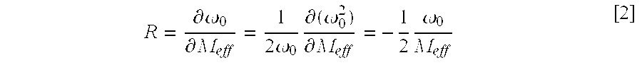
- Here δω 0 is the minimum resolvable frequency shift and R=δω0/δMeff is defined as the mass responsivity.
- To evaluate this expression we proceed as follows. The vibratory mass of the resonator is mode-specific, and is defined by the ratio M eff=Keff/ω0 2 where Keff=βEw(t/l)3 the effective force constant for the given mode and ω0=2πα(E/ρ)½(t/l2) is the mode's angular frequency. where w is the width of the beam, E is the elastic modulus of the beam, ρ is mass density of the beam, t is thickness of the beam, and l is length of the beam. For a doubly-clamped beam (cantilever) vibrating in its fundamental mode, α=1.05 (0.1615) and β=32 (0.67), hence Meff=β/(4π2α2)˜0.735 Mtot (0.65=Mtot) Here Mtot is the total mass of the resonator.
- The responsivity is then

- To make further progress, we must establish the minimum resolvable frequency shift, δω 0. As a rough estimate, we first consider the mass loading required to shift the resonance by its half width, i.e. to obtain δω0˜Δω=ω0/Qδω0˜ In this case we find,

- This first-pass crude analysis serves to illustrate an important point that remains true in the more detailed analyses that follow: the mass sensitivity is proportional to the ratio of the vibratory mass divided by its Q, the quality factor of the resonator. Hence, small, high quality factor resonators are optimal for mass detection. This illustrates the potential impact that nanoscale devices can offer for mass sensing applications. The sensitivity of a NEMS resonator to added mass can apparently be a very small fraction of its total mass if its Q is high.
- To obtain a better estimate we should write the minimum resolvable frequency as

- Here Δf˜2π/τ is the effective bandwidth, which depends upon the measurement averaging time, τ; and S f eff is the effective spectral density of the frequency fluctuations. The latter is comprised of processes intrinsically linked to the resonator itself (e.g. its phase noise and long term drift), as well as those introduced from the readout process. We shall denote these noise spectral densities Sf i and Sf (RO), respectively. In practice a resonator's frequency fluctuations depend upon its materials properties, geometry, and the experimental conditions (e.g. temperature, pressure, ambient gas species, etc.), and often little can be said about them that is truly generic. We shall not attempt to model these terms in the simple generalized discussion presented here.
- We can, however, make some concrete statements about the readout's contribution. We write S f (RO)=SV/(δV/δω)2 where SV is the spectral density of voltage noise at the output of the resonator's displacement transducer and (δV/δω) is the rate of change of the transducer output in the vicinity of the resonance frequency. We can crudely approximate the latter as.

- Here V max is the maximal response of the transducer (on resonance).
- In general, we perform mass sensing by driving the resonator, and looking for a frequency shift in steady-state. Hence V max implicitly depends upon the drive level, and to maximize the signal-to-noise ratio (SNR) one wishes to apply the largest drive level tolerable. For the sake of concreteness, we assume that this is the maximum r.m.s. level, <xmax>, still consistent with producing predominantly linear response. For both uniform and point loading of a doubly clamped beam, this can be approximated as <xmax>˜0.53 t, which depends only upon the beam thickness t in the direction of vibration. This, combined with the readout transducer responsivity, RT, (with units volts/meter), enables us to arrive at an expression for the maximum value of (δV/δω) expected:

- Thus, if we consider only the role of readout noise in determining the minimum resolvable frequency shift we obtain the
estimate 
- Note that this depends inversely upon the ratio of the transducer's maximum response to its noise floor (at the output), R T<xN>/[2πSV/T]½. Since this ratio defines the dynamic range (DR) of the coupled mechanical resonator/transducer system, we can write

- Note that the bandwidth chosen will affect DR.
- We can now write a simple expression for the mass sensitivity that is valid in the limit S f i<<Sf (RO) and hence the system noise is dominated by the readout,

- With this expression we first estimate the mass sensitivity attainable for our 32.8 MHz device. The relevant parameters for the system built using this SiC device are Q˜3000, DR˜60 dB for a 3 kHz bandwidth (T ˜2 ms), and M tot ˜8×10⁻¹² g. This leads to the approximate result that δM should be a few attograms (10−18 g), i.e. ˜106 Da, close to what is experimentally attained.
- This agreement gives us confidence to extrapolate to the sensitivity we expect should be attainable in the near term with further optimization of NEMS devices. Using a 200 MHz resonator with dimensions (w, t, l) of 0.1×0.05×1.4 μm, and M tot ˜2×10⁻¹⁴, assuming Q˜2×10⁴ and DR˜60 dB, one obtains 1.6×10²⁰ g. Our longer-term goal is a 850 MHz resonator, with dimensions 0.02×0.01×0.3 μm, and Mtot ˜2×10⁻¹⁶. Assuming that advances can be made to yield a slightly improved Q˜105 and DR˜80 dB at this frequency, one obtains 1.6×10⁻²⁴ g (1 Da). This would yield true atomic resolution, for a single adsorbed species, which need not be charged to be detected.
- Finally, we have repeated our measurements on several devices spanning a range of frequencies and vibratory mass values to demonstrate experimenatally attainable sensitivities. In these measurements, we extract the resonance frequency from experimentally obtained resonance line while the total resonator mass is changed by controlled, sequential pulses of Au deposition. The results are displayed in FIG. 6 and we summarize the estimated and experimental mass responsivity for these resonators in Table I. The estimates are based upon determination of the total resonator masses through direct measurement of their dimensions via electron microscopy. The inverse mass responsivity, is then estimated from the relation δM eff/δω0≅−1.47Mtot/ω0. FIG. 6 is a graph of the frequency shift curves for three additional devices with different fundamental frequencies as a function of the added mass, Δm. Each point corresponds to one deposition cycle. Table 1 below shows the parameters for these devices, and the predicted slopes, which are the inverse mass responsivities. The slope for the 72 MHz device corresponds to an experimental inverse mass responsivity of ˜51.5 kDa/Hz (80 zg/Hz, where 1 zg=10−21 g).
TABLE 1 
L × w × t (μm) Mtot(pg) 

11.4 0.8 × 0.259 × 36 2.8 MDa/Hz 1.2 MDa/Hz 26.2 32.8 0.67 × 0.259 × 8.7 235 kDa/Hz 165 kDa/Hz 14.2 56 0.65 × 0.259 × 12 7.1 115 kDa/Hz 118 kDa/Hz 72 0.65 × 0.259 × 10 6.0 73.5 kDa/Hz 51.5 kDa/Hz - These results clearly indicate the immense potential for NEMS-based mass spectrometry (NEMS-MS). Time-of-flight mass spectrometry (TOF-MS), the current mainstay in this field, is restricted to analysis of ionized species in the gas phase. In TOF-MS, gas phase ions are typically first created by a desorption/ionization technique such as plasma desorption (PD) or laser desorption (LD) and, subsequently, accelerated by an electric and/or magnetic field and directed into a drift tube. A detector ultimately records the time of flight of the ions within this tube, which depends on their m/Z ratios. An inherent, and important, limitation of this method is that the absolute mass itself is not accessible, but instead it is the ratio m/Z that is obtained. The mass resolution, m/Δm is determined by the spread in the initial distribution of the velocities of the ions upon desorption. This causes their arrival time, t at the detector, to involve a temporal uncertainty which can be characterized by its average magnitude Δt; hence m/Δm˜t/Δt. The best current TOF-MS systems have resolving power of order m/Δm˜10 4 to 105 for large molecules (M˜10-100 kDa). Further limitations are also imposed upon the size of molecules that can be handled with TOF-MS due to the need to ionize the analytes. Since the ionization energies are generally rather substantial, large molecules may fragment during such ionization. Moreover, the detection of such macromolecules constitutes a major challenge given that the efficiency of conventional particle detectors decreases rapidly with increasing mass. State-of-the-art cryogenic particle detectors cooled to temperatures approaching 100 mK have recently extended the range of MS up to the ˜1-10 MDa regime. An additional complication for ionization-based techniques is that they can be inefficient; often much of the analyzed material ends up electrically-neutral, and hence, undetectable. The amount of minimum sample material for a conclusive mass measurement, often referred to as the sensitivity of the MS, and can thus be rather appreciable.
- With attainment of single Dalton mass resolution, NEMS-MS will offer immense promise for mass spectrometry of individual macromolecules. In one possible implementation, a very low flux beam of neutral, gas phase species of the sample would impinge and adhere to a NEMS resonator. Individually resolved jumps in the resonance frequency of the NEMS device would directly indicate the mass of these adsorbing molecules. This approach offers the unique capability of mass spectrometry of individual neutral species. After a series of such measurements, the system could be regenerated by thermal desorption of the adsorbates.
- Even before single-Dalton resolution is attained, NEMS devices can provide significant enhancement of conventional mass spectrometry if employed as detectors for conventional TOF-MS. In such an implementation, with a NEMS resonator to detect single ion adsorption events, an arbitrarily large mass resolution would be achievable through signal averaging. Here, for ease of discussion, we describe the resolution improvement for a single component analyte in a matrix such in the MDa range. The “frequency dynamic range” of NEMS-MS is exceptionally large, and to a significant degree, essentially independent of the mass sensitivity, δM, that is determined by random frequency fluctuation processes. If the mass sensitivity is equal to, or better than the analyte mass, m, it becomes possible to count, individually, a large number, N>>1, of single molecule adsorption events, and to ultimately attain an effective mass resolution of, roughly, m/Δm˜m(N/δM). With the ˜1 MDa sensitivity demonstrated here, with sequential deposition of N˜10 6 individual 1 MDa species it will be possible to obtain a single Dalton resolution for this hybrid NEMS/TOF-MS. Apparently the resolving power in such a measurement will increase in direct proportion to the measured mass, unlike the case for conventional MS approaches. With NEMS detection, the minimum temporal separation between individual molecular sensing events is determined by the averaging time required to determine the instantaneous frequency to the desired measurement accuracy. For our 32.8 MHz experiment, the 2 ms averaging time would yield ˜1 Da sensitivity for ˜1 MDa species (m/Δm˜106) in ˜30 m. During this time the resonance frequency would shift by only ˜6.5 MHz. We have investigated the degradation in mass sensitivity of a NEMS resonator as it becomes heavily mass loaded. With sufficient adsorbed material (Pb) to shift the frequency of an (initially) ˜38.2 MHz resonator by ˜5 MHz, the Q was decreased by only a factor of order ˜10%. This immense “mass dynamic range” is one of the important attributes of the NEMS technique.
- In summary, even the simplest initial realizations of NEMS-MS described here appear to offer immense advances to the current state-of-the-art. Most notable are the significant increase in sensitivity, and the possibility of mass spectrometry of fragile molecules that are difficult to ionize non-destructively. NEMS-MS is unique in that it yields the absolute mass, rather than the m/Z ratio of an ion, and yields exceptionally large dynamic range for mass measurements. Additional advances in NEMS that appear to be realizable in the near term make feasible single-molecule NEMS-MS with 1 Da resolution. offering the exciting prospect of, in effect, “weighing” individual molecules.
- Many alterations and modifications may be made by those having ordinary skill in the art without departing from the spirit and scope of the invention. Therefore, it must be understood that the illustrated embodiment has been set forth only for the purposes of example and that it should not be taken as limiting the invention as defined by the following claims. For example, notwithstanding the fact that the elements of a claim are set forth below in a certain combination, it must be expressly understood that the invention includes other combinations of fewer, more or different elements, which are disclosed in above even when not initially claimed in such combinations.
- The words used in this specification to describe the invention and its various embodiments are to be understood not only in the sense of their commonly defined meanings, but to include by special definition in this specification structure, material or acts beyond the scope of the commonly defined meanings. Thus if an element can be understood in the context of this specification as including more than one meaning, then its use in a claim must be understood as being generic to all possible meanings supported by the specification and by the word itself.
- The definitions of the words or elements of the following claims are, therefore, defined in this specification to include not only the combination of elements which are literally set forth, but all equivalent structure, material or acts for performing substantially the same function in substantially the same way to obtain substantially the same result. In this sense it is therefore contemplated that an equivalent substitution of two or more elements may be made for any one of the elements in the claims below or that a single element may be substituted for two or more elements in a claim. Although elements may be described above as acting in certain combinations and even initially claimed as such, it is to be expressly understood that one or more elements from a claimed combination can in some cases be excised from the combination and that the claimed combination may be directed to a subcombination or variation of a subcombination.
- Insubstantial changes from the claimed subject matter as viewed by a person with ordinary skill in the art, now known or later devised, are expressly contemplated as being equivalently within the scope of the claims. Therefore, obvious substitutions now or later known to one with ordinary skill in the art are defined to be within the scope of the defined elements.
- The claims are thus to be understood to include what is specifically illustrated and described above, what is conceptionally equivalent, what can be obviously substituted and also what essentially incorporates the essential idea of the invention.
Claims (26)


Priority Applications (1)
| Application Number | Priority Date | Filing Date | Title |
|---|---|---|---|
| US10/138,538 US6722200B2 (en) | 2001-05-04 | 2002-05-03 | Apparatus and method for ultrasensitive nanoelectromechanical mass detection |
Applications Claiming Priority (2)
| Application Number | Priority Date | Filing Date | Title |
|---|---|---|---|
| US28874101P | 2001-05-04 | 2001-05-04 | |
| US10/138,538 US6722200B2 (en) | 2001-05-04 | 2002-05-03 | Apparatus and method for ultrasensitive nanoelectromechanical mass detection |
Publications (2)
| Publication Number | Publication Date |
|---|---|
| US20030033876A1 true US20030033876A1 (en) | 2003-02-20 |
| US6722200B2 US6722200B2 (en) | 2004-04-20 |
Family
ID=23108444
Family Applications (1)
| Application Number | Title | Priority Date | Filing Date |
|---|---|---|---|
| US10/138,538 Expired - Lifetime US6722200B2 (en) | 2001-05-04 | 2002-05-03 | Apparatus and method for ultrasensitive nanoelectromechanical mass detection |
Country Status (5)
| Country | Link |
|---|---|
| US (1) | US6722200B2 (en) |
| EP (1) | EP1390287A2 (en) |
| AU (1) | AU2002314767A1 (en) |
| CA (1) | CA2446353A1 (en) |
| WO (1) | WO2002090246A2 (en) |
Cited By (25)
| Publication number | Priority date | Publication date | Assignee | Title |
|---|---|---|---|---|
| US20030151257A1 (en) * | 2001-06-20 | 2003-08-14 | Ambient Systems, Inc. | Energy conversion systems using nanometer scale assemblies and methods for using same |
| WO2003095617A2 (en) * | 2002-05-07 | 2003-11-20 | California Institute Of Technology | A method and apparatus for providing signal analysis of a bionems resonator or transducer |
| US20040240252A1 (en) * | 2003-06-02 | 2004-12-02 | Pinkerton Joseph F. | Nanoelectromechanical memory cells and data storage devices |
| US20040239210A1 (en) * | 2003-06-02 | 2004-12-02 | Pinkerton Joseph F. | Electrical assemblies using molecular-scale electrically conductive and mechanically flexible beams and methods for application of same |
| US20040238907A1 (en) * | 2003-06-02 | 2004-12-02 | Pinkerton Joseph F. | Nanoelectromechanical transistors and switch systems |
| US20050081635A1 (en) * | 2003-03-14 | 2005-04-21 | Yoshihiro Kobayashi | Measuring method, measurement-signal output circuit, and measuring apparatus |
| US20050262943A1 (en) * | 2004-05-27 | 2005-12-01 | Glenn Claydon | Apparatus, methods, and systems to detect an analyte based on changes in a resonant frequency of a spring element |
| EP1607725A1 (en) * | 2003-03-25 | 2005-12-21 | Seiko Epson Corporation | Mass measuring method, circuit for exciting piezoelectric vibratory piece for mass measurement, and mass measuring instrument |
| US20070048160A1 (en) * | 2005-07-19 | 2007-03-01 | Pinkerton Joseph F | Heat activated nanometer-scale pump |
| CN100425524C (en) * | 2006-01-13 | 2008-10-15 | 中国科学院上海微系统与信息技术研究所 | Electromagnet excitated high order mode silicon micromechanical cantilever driving structure, its production method and uses |
| US20080251865A1 (en) * | 2007-04-03 | 2008-10-16 | Pinkerton Joseph F | Nanoelectromechanical systems and methods for making the same |
| US7495350B2 (en) | 2003-06-02 | 2009-02-24 | Cjp Ip Holdings, Ltd. | Energy conversion systems utilizing parallel array of automatic switches and generators |
| US7518283B2 (en) | 2004-07-19 | 2009-04-14 | Cjp Ip Holdings Ltd. | Nanometer-scale electrostatic and electromagnetic motors and generators |
| US20090261241A1 (en) * | 2008-01-25 | 2009-10-22 | California Institute Of Technology | Single molecule mass spectroscopy enabled by nanoelectromechanical systems (nems-ms) |
| EP2233919A1 (en) * | 2009-03-26 | 2010-09-29 | Commissariat à l'Énergie Atomique et aux Énergies Alternatives | Micro-device for in situ detection of particles of interest in a fluid medium and method for implementing the same |
| KR101229730B1 (en) | 2010-02-18 | 2013-02-04 | 국립대학법인 울산과학기술대학교 산학협력단 | Mass sensor using graphene sheet and method for measuring mass |
| US20140312980A1 (en) * | 2013-04-17 | 2014-10-23 | Commissariat A L'energie Atomique Et Aux Energies Alternatives | Circuit for measuring the resonant frequency of nanoresonators |
| EP2884520A1 (en) * | 2013-12-12 | 2015-06-17 | Acreo Swedish ICT AB | Nano mass spectrometry |
| WO2016118821A1 (en) * | 2015-01-23 | 2016-07-28 | California Institute Of Technology | Integrated hybrid nems mass spectrometry |
| US20170117905A1 (en) * | 2014-10-28 | 2017-04-27 | Massachusetts Institute Of Technology | Simultaneous oscillation and frequency tracking of multiple resonances via digitally implemented phase-locked loop array |
| US9660654B2 (en) | 2012-10-26 | 2017-05-23 | California Institute Of Technology | Synchronization of nanomechanical oscillators |
| US11162886B2 (en) | 2017-03-31 | 2021-11-02 | Massachusetts Institute Of Technology | Systems, articles, and methods for flowing particles |
| US20220050064A1 (en) * | 2019-02-11 | 2022-02-17 | California Institute Of Technology | Highly-multiplexed nems-array readout system based on superconducting cavity optomechanics |
| US11346755B2 (en) | 2019-01-10 | 2022-05-31 | Travera, Inc. | Calibration of a functional biomarker instrument |
| US11754486B2 (en) | 2017-06-19 | 2023-09-12 | Massachusetts Institute Of Technology | Systems and methods for measuring properties of particles |
Families Citing this family (38)
| Publication number | Priority date | Publication date | Assignee | Title |
|---|---|---|---|---|
| US7375321B2 (en) | 2000-08-09 | 2008-05-20 | California Institute Of Technology | Dynamics bionems sensors and arrays of bionems sensor immersed in fluids |
| JP3764853B2 (en) * | 2001-05-28 | 2006-04-12 | 喜萬 中山 | Nanomaterial mass measurement method and apparatus |
| WO2004041998A2 (en) * | 2002-05-07 | 2004-05-21 | California Institute Of Technology | Nanomechanichal energy, force, and mass sensors |
| JP4437699B2 (en) * | 2004-05-14 | 2010-03-24 | 富士通マイクロエレクトロニクス株式会社 | Sensor |
| US7598723B2 (en) * | 2005-02-14 | 2009-10-06 | Clemson University | Method and apparatus for detecting resonance in electrostatically driven elements |
| US8384372B1 (en) | 2005-02-14 | 2013-02-26 | Clemson University | Non-linear electrical actuation and detection |
| EP1913800A4 (en) * | 2005-07-27 | 2016-09-21 | Wisconsin Alumni Res Found | Nanoelectromechanical and microelectromechanical sensors and analyzers |
| US7923533B2 (en) * | 2006-06-29 | 2011-04-12 | The Invention Science Fund I, Llc | Methods for arbitrary peptide synthesis |
| US7777002B2 (en) * | 2006-06-29 | 2010-08-17 | The Invention Science Fund I, Llc | Methods for arbitrary peptide synthesis |
| US20080004813A1 (en) * | 2006-06-29 | 2008-01-03 | Searete Llc, A Limited Liability Corporation Of The State Of Delaware | Systems for arbitrary peptide synthesis |
| US7879975B2 (en) * | 2006-06-29 | 2011-02-01 | The Invention Science Fund I, Llc | Methods for arbitrary peptide synthesis |
| US7910695B2 (en) * | 2006-06-29 | 2011-03-22 | The Invention Science Fund I, Llc | Methods for arbitrary peptide synthesis |
| US7555938B2 (en) * | 2006-09-19 | 2009-07-07 | California Institute Of Technology | Thermoelastic self-actuation in piezoresistive resonators |
| US7900527B1 (en) | 2006-12-22 | 2011-03-08 | University Of Central Florida Research Foundation, Inc. | Electrically deflected nanomechanical sensors |
| US7724103B2 (en) * | 2007-02-13 | 2010-05-25 | California Institute Of Technology | Ultra-high frequency self-sustaining oscillators, coupled oscillators, voltage-controlled oscillators, and oscillator arrays based on vibrating nanoelectromechanical resonators |
| US7884324B2 (en) * | 2007-06-03 | 2011-02-08 | Wisconsin Alumni Research Foundation | Nanopillar arrays for electron emission |
| WO2009038579A2 (en) * | 2007-09-19 | 2009-03-26 | California Institute Of Technology | Thermoelastic self-actuation in piezoresistive resonators |
| EP2141490B1 (en) * | 2008-07-02 | 2015-04-01 | Stichting IMEC Nederland | Chemical sensing microbeam device |
| US8584524B2 (en) * | 2008-10-21 | 2013-11-19 | ISC8 Inc. | Nano-resonator inertial sensor assembly |
| US8441635B2 (en) * | 2009-03-24 | 2013-05-14 | Nutech Ventures | Mass sensor |
| US20110113856A1 (en) * | 2009-11-13 | 2011-05-19 | Honeywell International | All-differential resonant nanosensor apparatus and method |
| US8479560B2 (en) | 2010-03-30 | 2013-07-09 | Honeywell International Inc. | Differential resonant sensor apparatus and method for detecting relative humidity |
| US8742333B2 (en) | 2010-09-17 | 2014-06-03 | Wisconsin Alumni Research Foundation | Method to perform beam-type collision-activated dissociation in the pre-existing ion injection pathway of a mass spectrometer |
| US8507845B2 (en) | 2011-06-02 | 2013-08-13 | Wisconsin Alumni Research Foundation | Membrane detector for time-of-flight mass spectrometry |
| US9347815B2 (en) | 2012-05-09 | 2016-05-24 | California Institute Of Technology | Single-protein nanomechanical mass spectrometry in real time |
| FR2994777B1 (en) * | 2012-08-22 | 2014-08-22 | Commissariat Energie Atomique | NANO-RESONATOR RESONANCE FREQUENCY MEASUREMENT CIRCUIT |
| WO2014107173A1 (en) * | 2013-01-02 | 2014-07-10 | California Institute Of Technology | Piezoresistive nems resonator array |
| EP2959274A2 (en) | 2013-02-22 | 2015-12-30 | California Institute of Technology | Shape analysis and mass spectrometry of individual molecules by nanomechanical systems |
| FR3003083B1 (en) | 2013-03-11 | 2015-04-10 | Commissariat Energie Atomique | DEVICE FOR DETERMINING THE MASS OF A PARTICLE IN SUSPENSION OR SOLUTION IN A FLUID |
| WO2014204433A1 (en) * | 2013-06-17 | 2014-12-24 | Empire Technology Development Llc | Graded films |
| GB2518185A (en) | 2013-09-12 | 2015-03-18 | Ibm | Electromechanical switching device wtih 2D layered material surfaces |
| WO2015082956A1 (en) * | 2013-12-02 | 2015-06-11 | Commissariat A L'energie Atomique Et Aux Energies Alternatives | System and method for analyzing a gas |
| US10126266B2 (en) | 2014-12-29 | 2018-11-13 | Concentric Meter Corporation | Fluid parameter sensor and meter |
| US10107784B2 (en) | 2014-12-29 | 2018-10-23 | Concentric Meter Corporation | Electromagnetic transducer |
| US9752911B2 (en) | 2014-12-29 | 2017-09-05 | Concentric Meter Corporation | Fluid parameter sensor and meter |
| US10845283B2 (en) | 2016-03-31 | 2020-11-24 | King Abdullah University Of Science And Technology | Active MEMS microbeam device for gas detection |
| US10830738B2 (en) | 2016-11-14 | 2020-11-10 | University Of Alberta | Ultrasensitive high Q-factor AT-cut-quartz crystal microbalance femtogram mass sensor |
| US11289319B2 (en) | 2019-08-06 | 2022-03-29 | Thermo Fisher Scientific (Bremen) Gmbh | System to analyze particles, and particularly the mass of particles |
Citations (3)
| Publication number | Priority date | Publication date | Assignee | Title |
|---|---|---|---|---|
| US6389877B1 (en) * | 1997-12-26 | 2002-05-21 | Ngk Insulators, Ltd. | Double-headed mass sensor and mass detection method |
| US6457360B1 (en) * | 2001-02-21 | 2002-10-01 | Conel Ltd. | High-precision integrated semiconductor peizoresistive detector devices and methods using the same |
| US6457361B1 (en) * | 1998-09-04 | 2002-10-01 | Ngk Insulators, Ltd. | Mass sensor and mass sensing method |
Family Cites Families (4)
| Publication number | Priority date | Publication date | Assignee | Title |
|---|---|---|---|---|
| US4905701A (en) * | 1988-06-15 | 1990-03-06 | National Research Development Corporation | Apparatus and method for detecting small changes in attached mass of piezoelectric devices used as sensors |
| US5201215A (en) * | 1991-10-17 | 1993-04-13 | The United States Of America As Represented By The United States Department Of Energy | Method for simultaneous measurement of mass loading and fluid property changes using a quartz crystal microbalance |
| US5914553A (en) * | 1997-06-16 | 1999-06-22 | Cornell Research Foundation, Inc. | Multistable tunable micromechanical resonators |
| JP2000180250A (en) * | 1998-10-09 | 2000-06-30 | Ngk Insulators Ltd | Mass sensor and mass detection method |
-
2002
- 2002-05-03 AU AU2002314767A patent/AU2002314767A1/en not_active Abandoned
- 2002-05-03 WO PCT/US2002/014130 patent/WO2002090246A2/en not_active Application Discontinuation
- 2002-05-03 EP EP02741690A patent/EP1390287A2/en not_active Withdrawn
- 2002-05-03 US US10/138,538 patent/US6722200B2/en not_active Expired - Lifetime
- 2002-05-03 CA CA002446353A patent/CA2446353A1/en not_active Abandoned
Patent Citations (3)
| Publication number | Priority date | Publication date | Assignee | Title |
|---|---|---|---|---|
| US6389877B1 (en) * | 1997-12-26 | 2002-05-21 | Ngk Insulators, Ltd. | Double-headed mass sensor and mass detection method |
| US6457361B1 (en) * | 1998-09-04 | 2002-10-01 | Ngk Insulators, Ltd. | Mass sensor and mass sensing method |
| US6457360B1 (en) * | 2001-02-21 | 2002-10-01 | Conel Ltd. | High-precision integrated semiconductor peizoresistive detector devices and methods using the same |
Cited By (52)
| Publication number | Priority date | Publication date | Assignee | Title |
|---|---|---|---|---|
| US7262515B2 (en) | 2001-06-20 | 2007-08-28 | Ambient Systems, Inc. | Energy conversion systems using nanometer scale assemblies and methods for using same |
| US20030151257A1 (en) * | 2001-06-20 | 2003-08-14 | Ambient Systems, Inc. | Energy conversion systems using nanometer scale assemblies and methods for using same |
| US7414325B2 (en) | 2001-06-20 | 2008-08-19 | Ambient Systems, Inc. | Energy conversion systems using nanometer scale assemblies and methods for using same |
| WO2003095617A2 (en) * | 2002-05-07 | 2003-11-20 | California Institute Of Technology | A method and apparatus for providing signal analysis of a bionems resonator or transducer |
| WO2003095617A3 (en) * | 2002-05-07 | 2004-04-29 | California Inst Of Techn | A method and apparatus for providing signal analysis of a bionems resonator or transducer |
| US7165452B2 (en) | 2003-03-14 | 2007-01-23 | Seiko Epson Corporation | Measuring method, measurement-signal output circuit, and measuring apparatus |
| US20050081635A1 (en) * | 2003-03-14 | 2005-04-21 | Yoshihiro Kobayashi | Measuring method, measurement-signal output circuit, and measuring apparatus |
| EP1605246A4 (en) * | 2003-03-14 | 2006-06-21 | Seiko Epson Corp | Measuring method, measuring signal output circuit, and measuring apparatus |
| EP1605246A1 (en) * | 2003-03-14 | 2005-12-14 | Seiko Epson Corporation | Measuring method, measuring signal output circuit, and measuring apparatus |
| EP1607725A1 (en) * | 2003-03-25 | 2005-12-21 | Seiko Epson Corporation | Mass measuring method, circuit for exciting piezoelectric vibratory piece for mass measurement, and mass measuring instrument |
| EP1607725A4 (en) * | 2003-03-25 | 2007-09-19 | Seiko Epson Corp | Mass measuring method, circuit for exciting piezoelectric vibratory piece for mass measurement, and mass measuring instrument |
| US7196450B2 (en) | 2003-06-02 | 2007-03-27 | Ambient Systems, Inc. | Electromechanical assemblies using molecular-scale electrically conductive and mechanically flexible beams and methods for application of same |
| US7256063B2 (en) | 2003-06-02 | 2007-08-14 | Ambient Systems, Inc. | Nanoelectromechanical transistors and switch systems |
| US7095645B2 (en) | 2003-06-02 | 2006-08-22 | Ambient Systems, Inc. | Nanoelectromechanical memory cells and data storage devices |
| US7495350B2 (en) | 2003-06-02 | 2009-02-24 | Cjp Ip Holdings, Ltd. | Energy conversion systems utilizing parallel array of automatic switches and generators |
| US7582992B2 (en) | 2003-06-02 | 2009-09-01 | Cjp Ip Holdings, Ltd. | Electrical assemblies using molecular-scale electrically conductive and mechanically flexible beams and methods for application of same |
| US20050179339A1 (en) * | 2003-06-02 | 2005-08-18 | Ambient Systems, Inc. | Electromechanical assemblies using molecular-scale electrically conductive and mechanically flexible beams and methods for application of same |
| US7199498B2 (en) * | 2003-06-02 | 2007-04-03 | Ambient Systems, Inc. | Electrical assemblies using molecular-scale electrically conductive and mechanically flexible beams and methods for application of same |
| US20070138888A1 (en) * | 2003-06-02 | 2007-06-21 | Pinkerton Joseph F | Electrical assemblies using molecular-scale electrically conductive and mechanically flexible beams and methods for application of same |
| US20070177418A1 (en) * | 2003-06-02 | 2007-08-02 | Ambient Systems, Inc. | Nanoelectromechanical memory cells and data storage devices |
| US20040240252A1 (en) * | 2003-06-02 | 2004-12-02 | Pinkerton Joseph F. | Nanoelectromechanical memory cells and data storage devices |
| US20040238907A1 (en) * | 2003-06-02 | 2004-12-02 | Pinkerton Joseph F. | Nanoelectromechanical transistors and switch systems |
| US20050104085A1 (en) * | 2003-06-02 | 2005-05-19 | Ambient Systems, Inc. | Nanoelectromechanical transistors and switch systems |
| US7362605B2 (en) | 2003-06-02 | 2008-04-22 | Ambient Systems, Inc. | Nanoelectromechanical memory cells and data storage devices |
| US20040239210A1 (en) * | 2003-06-02 | 2004-12-02 | Pinkerton Joseph F. | Electrical assemblies using molecular-scale electrically conductive and mechanically flexible beams and methods for application of same |
| US20050262943A1 (en) * | 2004-05-27 | 2005-12-01 | Glenn Claydon | Apparatus, methods, and systems to detect an analyte based on changes in a resonant frequency of a spring element |
| US7518283B2 (en) | 2004-07-19 | 2009-04-14 | Cjp Ip Holdings Ltd. | Nanometer-scale electrostatic and electromagnetic motors and generators |
| US20070048160A1 (en) * | 2005-07-19 | 2007-03-01 | Pinkerton Joseph F | Heat activated nanometer-scale pump |
| CN100425524C (en) * | 2006-01-13 | 2008-10-15 | 中国科学院上海微系统与信息技术研究所 | Electromagnet excitated high order mode silicon micromechanical cantilever driving structure, its production method and uses |
| US20080251865A1 (en) * | 2007-04-03 | 2008-10-16 | Pinkerton Joseph F | Nanoelectromechanical systems and methods for making the same |
| US7839028B2 (en) | 2007-04-03 | 2010-11-23 | CJP IP Holding, Ltd. | Nanoelectromechanical systems and methods for making the same |
| US8385113B2 (en) | 2007-04-03 | 2013-02-26 | Cjp Ip Holdings, Ltd. | Nanoelectromechanical systems and methods for making the same |
| US20090261241A1 (en) * | 2008-01-25 | 2009-10-22 | California Institute Of Technology | Single molecule mass spectroscopy enabled by nanoelectromechanical systems (nems-ms) |
| US8227747B2 (en) * | 2008-01-25 | 2012-07-24 | California Institute Of Technology | Single molecule mass spectroscopy enabled by nanoelectromechanical systems (NEMS-MS) |
| EP2233919A1 (en) * | 2009-03-26 | 2010-09-29 | Commissariat à l'Énergie Atomique et aux Énergies Alternatives | Micro-device for in situ detection of particles of interest in a fluid medium and method for implementing the same |
| US20100244855A1 (en) * | 2009-03-26 | 2010-09-30 | Commissariat A L'energie Atomique Et Aux Energies Alternatives | Microdevice for the In Situ Detection of Particles of Interest in a Fluid Medium and Operating Method |
| FR2943787A1 (en) * | 2009-03-26 | 2010-10-01 | Commissariat Energie Atomique | MICRO-DEVICE FOR IN SITU DETECTION OF PARTICLES OF INTEREST IN A FLUID MEDIUM, AND METHOD FOR CARRYING OUT SAID METHOD |
| US8334702B2 (en) | 2009-03-26 | 2012-12-18 | Commissariat a l'Energie et aux Energies Alternatives | Microdevice for the in situ detection of particles of interest in a fluid medium and operating method |
| KR101229730B1 (en) | 2010-02-18 | 2013-02-04 | 국립대학법인 울산과학기술대학교 산학협력단 | Mass sensor using graphene sheet and method for measuring mass |
| US9660654B2 (en) | 2012-10-26 | 2017-05-23 | California Institute Of Technology | Synchronization of nanomechanical oscillators |
| US9100025B2 (en) * | 2013-04-17 | 2015-08-04 | Commissariat A L'energie Atomique Et Aux Energies Alternatives | Circuit for measuring the resonant frequency of nanoresonators |
| US20140312980A1 (en) * | 2013-04-17 | 2014-10-23 | Commissariat A L'energie Atomique Et Aux Energies Alternatives | Circuit for measuring the resonant frequency of nanoresonators |
| EP2884520A1 (en) * | 2013-12-12 | 2015-06-17 | Acreo Swedish ICT AB | Nano mass spectrometry |
| US20170117905A1 (en) * | 2014-10-28 | 2017-04-27 | Massachusetts Institute Of Technology | Simultaneous oscillation and frequency tracking of multiple resonances via digitally implemented phase-locked loop array |
| US11143548B2 (en) | 2014-10-28 | 2021-10-12 | Massachusetts Institute Of Technology | Simultaneous oscillation and frequency tracking of multiple resonances via digitally implemented phase-locked loop array |
| WO2016118821A1 (en) * | 2015-01-23 | 2016-07-28 | California Institute Of Technology | Integrated hybrid nems mass spectrometry |
| US10381206B2 (en) | 2015-01-23 | 2019-08-13 | California Institute Of Technology | Integrated hybrid NEMS mass spectrometry |
| US11162886B2 (en) | 2017-03-31 | 2021-11-02 | Massachusetts Institute Of Technology | Systems, articles, and methods for flowing particles |
| US11754486B2 (en) | 2017-06-19 | 2023-09-12 | Massachusetts Institute Of Technology | Systems and methods for measuring properties of particles |
| US11346755B2 (en) | 2019-01-10 | 2022-05-31 | Travera, Inc. | Calibration of a functional biomarker instrument |
| US20220050064A1 (en) * | 2019-02-11 | 2022-02-17 | California Institute Of Technology | Highly-multiplexed nems-array readout system based on superconducting cavity optomechanics |
| US11624715B2 (en) * | 2019-02-11 | 2023-04-11 | California Institute Of Technology | Highly-multiplexed NEMS-array readout system based on superconducting cavity optomechanics |
Also Published As
| Publication number | Publication date |
|---|---|
| CA2446353A1 (en) | 2002-11-14 |
| US6722200B2 (en) | 2004-04-20 |
| WO2002090246A3 (en) | 2003-03-13 |
| AU2002314767A1 (en) | 2002-11-18 |
| WO2002090246A2 (en) | 2002-11-14 |
| EP1390287A2 (en) | 2004-02-25 |
Similar Documents
| Publication | Publication Date | Title |
|---|---|---|
| US6722200B2 (en) | Apparatus and method for ultrasensitive nanoelectromechanical mass detection | |
| Ekinci et al. | Ultrasensitive nanoelectromechanical mass detection | |
| Mochida et al. | A micromachined vibrating rate gyroscope with independent beams for the drive and detection modes | |
| d’Urso et al. | Feedback cooling of a one-electron oscillator | |
| Li et al. | Ultra-sensitive NEMS magnetoelectric sensor for picotesla DC magnetic field detection | |
| US9599495B2 (en) | Thermal flow sensor with vibrating element and gas sensor comprising at least one such sensor | |
| Forsen et al. | Ultrasensitive mass sensor fully integrated with complementary metal-oxide-semiconductor circuitry | |
| Ekinci et al. | Ultimate limits to inertial mass sensing based upon nanoelectromechanical systems | |
| US7168298B1 (en) | Mass-sensitive chemical preconcentrator | |
| US9945822B2 (en) | Measurement system including a network of nanoelectromechanical system resonators | |
| US8227747B2 (en) | Single molecule mass spectroscopy enabled by nanoelectromechanical systems (NEMS-MS) | |
| US9347815B2 (en) | Single-protein nanomechanical mass spectrometry in real time | |
| US5684276A (en) | Micromechanical oscillating mass balance | |
| JP2006506236A (en) | Apparatus and method for use in vacuum-based sensors of micromechanical energy, force and mass | |
| Davis et al. | Aluminum nanocantilevers for high sensitivity mass sensors | |
| Askari et al. | Near-navigation grade quad mass gyroscope with Q-factor limited by thermo-elastic damping | |
| JP2006030195A (en) | Magnetometer having electromechanical resonator | |
| D’Urso et al. | Single-particle self-excited oscillator | |
| Borrielli et al. | Wideband mechanical response of a high-Q silicon double-paddle oscillator | |
| Narducci et al. | Sensitivity improvement of a microcantilever based mass sensor | |
| Tsuchiya et al. | Vibrating gyroscope consisting of three layers of polysilicon thin films | |
| Gaillard et al. | Electrical detection of oscillations in microcantilevers and nanocantilevers | |
| JP2011043459A (en) | Mechanical detector and measuring method | |
| Xu et al. | A micro resonant gas sensor with adjustable natural frequency | |
| Liao et al. | Resonance frequency tracking and measuring system for micro-electromechanical cantilever array sensors |
Legal Events
| Date | Code | Title | Description |
|---|---|---|---|
| AS | Assignment |
Owner name: CALIFORNIA INSTITUTE OF TECHNOLOGY, CALIFORNIA Free format text: ASSIGNMENT OF ASSIGNORS INTEREST;ASSIGNORS:ROUKES, MICHAEL L.;EKINCI, KAMIL L.;REEL/FRAME:012981/0282;SIGNING DATES FROM 20020506 TO 20020522 |
|
| AS | Assignment |
Owner name: DARPA, VIRGINIA Free format text: CONFIRMATORY LICENSE;ASSIGNOR:CALIFORNIA INSTITUE OF TECHNOLOGY;REEL/FRAME:013040/0151 Effective date: 20020624 |
|
| STCF | Information on status: patent grant |
Free format text: PATENTED CASE |
|
| FEPP | Fee payment procedure |
Free format text: PAYOR NUMBER ASSIGNED (ORIGINAL EVENT CODE: ASPN); ENTITY STATUS OF PATENT OWNER: SMALL ENTITY |
|
| FPAY | Fee payment |
Year of fee payment: 4 |
|
| FPAY | Fee payment |
Year of fee payment: 8 |
|
| FEPP | Fee payment procedure |
Free format text: PAYER NUMBER DE-ASSIGNED (ORIGINAL EVENT CODE: RMPN); ENTITY STATUS OF PATENT OWNER: SMALL ENTITY Free format text: PAYOR NUMBER ASSIGNED (ORIGINAL EVENT CODE: ASPN); ENTITY STATUS OF PATENT OWNER: SMALL ENTITY |
|
| FPAY | Fee payment |
Year of fee payment: 12 |