US20020159686A1 - Optical channel selector - Google Patents
Optical channel selector Download PDFInfo
- Publication number
- US20020159686A1 US20020159686A1 US09/238,222 US23822299A US2002159686A1 US 20020159686 A1 US20020159686 A1 US 20020159686A1 US 23822299 A US23822299 A US 23822299A US 2002159686 A1 US2002159686 A1 US 2002159686A1
- Authority
- US
- United States
- Prior art keywords
- channel
- optical
- feedback path
- pass
- splitter
- Prior art date
- Legal status (The legal status is an assumption and is not a legal conclusion. Google has not performed a legal analysis and makes no representation as to the accuracy of the status listed.)
- Granted
Links
- 230000003287 optical effect Effects 0.000 title claims abstract description 220
- 230000004044 response Effects 0.000 claims abstract description 43
- 238000004891 communication Methods 0.000 claims abstract description 26
- 230000005540 biological transmission Effects 0.000 claims description 22
- 238000000034 method Methods 0.000 claims description 11
- 238000002310 reflectometry Methods 0.000 claims description 8
- 230000008878 coupling Effects 0.000 description 19
- 238000010168 coupling process Methods 0.000 description 19
- 238000005859 coupling reaction Methods 0.000 description 19
- 230000010363 phase shift Effects 0.000 description 11
- 238000013461 design Methods 0.000 description 7
- 239000013307 optical fiber Substances 0.000 description 7
- 230000000737 periodic effect Effects 0.000 description 5
- 230000007547 defect Effects 0.000 description 4
- 230000001419 dependent effect Effects 0.000 description 4
- 230000003595 spectral effect Effects 0.000 description 4
- 230000008859 change Effects 0.000 description 2
- 239000010409 thin film Substances 0.000 description 2
- 238000012546 transfer Methods 0.000 description 2
- 230000015572 biosynthetic process Effects 0.000 description 1
- 230000001427 coherent effect Effects 0.000 description 1
- 230000000295 complement effect Effects 0.000 description 1
- 239000003989 dielectric material Substances 0.000 description 1
- 230000000694 effects Effects 0.000 description 1
- 230000014509 gene expression Effects 0.000 description 1
- 239000000463 material Substances 0.000 description 1
- 238000012545 processing Methods 0.000 description 1
- 230000000644 propagated effect Effects 0.000 description 1
- 230000000717 retained effect Effects 0.000 description 1
- 230000006641 stabilisation Effects 0.000 description 1
- 238000011105 stabilization Methods 0.000 description 1
- 238000003786 synthesis reaction Methods 0.000 description 1
- 230000007704 transition Effects 0.000 description 1
Images


Classifications
-
- H—ELECTRICITY
- H04—ELECTRIC COMMUNICATION TECHNIQUE
- H04Q—SELECTING
- H04Q11/00—Selecting arrangements for multiplex systems
- H04Q11/0001—Selecting arrangements for multiplex systems using optical switching
- H04Q11/0005—Switch and router aspects
-
- B—PERFORMING OPERATIONS; TRANSPORTING
- B82—NANOTECHNOLOGY
- B82Y—SPECIFIC USES OR APPLICATIONS OF NANOSTRUCTURES; MEASUREMENT OR ANALYSIS OF NANOSTRUCTURES; MANUFACTURE OR TREATMENT OF NANOSTRUCTURES
- B82Y20/00—Nanooptics, e.g. quantum optics or photonic crystals
-
- G—PHYSICS
- G02—OPTICS
- G02B—OPTICAL ELEMENTS, SYSTEMS OR APPARATUS
- G02B6/00—Light guides; Structural details of arrangements comprising light guides and other optical elements, e.g. couplings
- G02B6/10—Light guides; Structural details of arrangements comprising light guides and other optical elements, e.g. couplings of the optical waveguide type
- G02B6/12—Light guides; Structural details of arrangements comprising light guides and other optical elements, e.g. couplings of the optical waveguide type of the integrated circuit kind
- G02B6/12007—Light guides; Structural details of arrangements comprising light guides and other optical elements, e.g. couplings of the optical waveguide type of the integrated circuit kind forming wavelength selective elements, e.g. multiplexer, demultiplexer
-
- G—PHYSICS
- G02—OPTICS
- G02B—OPTICAL ELEMENTS, SYSTEMS OR APPARATUS
- G02B6/00—Light guides; Structural details of arrangements comprising light guides and other optical elements, e.g. couplings
- G02B6/10—Light guides; Structural details of arrangements comprising light guides and other optical elements, e.g. couplings of the optical waveguide type
- G02B6/12—Light guides; Structural details of arrangements comprising light guides and other optical elements, e.g. couplings of the optical waveguide type of the integrated circuit kind
- G02B6/122—Basic optical elements, e.g. light-guiding paths
- G02B6/1225—Basic optical elements, e.g. light-guiding paths comprising photonic band-gap structures or photonic lattices
-
- G—PHYSICS
- G02—OPTICS
- G02B—OPTICAL ELEMENTS, SYSTEMS OR APPARATUS
- G02B6/00—Light guides; Structural details of arrangements comprising light guides and other optical elements, e.g. couplings
- G02B6/24—Coupling light guides
- G02B6/26—Optical coupling means
- G02B6/28—Optical coupling means having data bus means, i.e. plural waveguides interconnected and providing an inherently bidirectional system by mixing and splitting signals
- G02B6/2804—Optical coupling means having data bus means, i.e. plural waveguides interconnected and providing an inherently bidirectional system by mixing and splitting signals forming multipart couplers without wavelength selective elements, e.g. "T" couplers, star couplers
- G02B6/2861—Optical coupling means having data bus means, i.e. plural waveguides interconnected and providing an inherently bidirectional system by mixing and splitting signals forming multipart couplers without wavelength selective elements, e.g. "T" couplers, star couplers using fibre optic delay lines and optical elements associated with them, e.g. for use in signal processing, e.g. filtering
-
- G—PHYSICS
- G02—OPTICS
- G02B—OPTICAL ELEMENTS, SYSTEMS OR APPARATUS
- G02B6/00—Light guides; Structural details of arrangements comprising light guides and other optical elements, e.g. couplings
- G02B6/24—Coupling light guides
- G02B6/26—Optical coupling means
- G02B6/28—Optical coupling means having data bus means, i.e. plural waveguides interconnected and providing an inherently bidirectional system by mixing and splitting signals
- G02B6/293—Optical coupling means having data bus means, i.e. plural waveguides interconnected and providing an inherently bidirectional system by mixing and splitting signals with wavelength selective means
- G02B6/29304—Optical coupling means having data bus means, i.e. plural waveguides interconnected and providing an inherently bidirectional system by mixing and splitting signals with wavelength selective means operating by diffraction, e.g. grating
- G02B6/29316—Light guides comprising a diffractive element, e.g. grating in or on the light guide such that diffracted light is confined in the light guide
- G02B6/29317—Light guides of the optical fibre type
- G02B6/29319—With a cascade of diffractive elements or of diffraction operations
-
- G—PHYSICS
- G02—OPTICS
- G02B—OPTICAL ELEMENTS, SYSTEMS OR APPARATUS
- G02B6/00—Light guides; Structural details of arrangements comprising light guides and other optical elements, e.g. couplings
- G02B6/24—Coupling light guides
- G02B6/26—Optical coupling means
- G02B6/28—Optical coupling means having data bus means, i.e. plural waveguides interconnected and providing an inherently bidirectional system by mixing and splitting signals
- G02B6/293—Optical coupling means having data bus means, i.e. plural waveguides interconnected and providing an inherently bidirectional system by mixing and splitting signals with wavelength selective means
- G02B6/29331—Optical coupling means having data bus means, i.e. plural waveguides interconnected and providing an inherently bidirectional system by mixing and splitting signals with wavelength selective means operating by evanescent wave coupling
- G02B6/29335—Evanescent coupling to a resonator cavity, i.e. between a waveguide mode and a resonant mode of the cavity
- G02B6/29338—Loop resonators
- G02B6/29343—Cascade of loop resonators
-
- G—PHYSICS
- G02—OPTICS
- G02B—OPTICAL ELEMENTS, SYSTEMS OR APPARATUS
- G02B6/00—Light guides; Structural details of arrangements comprising light guides and other optical elements, e.g. couplings
- G02B6/24—Coupling light guides
- G02B6/26—Optical coupling means
- G02B6/28—Optical coupling means having data bus means, i.e. plural waveguides interconnected and providing an inherently bidirectional system by mixing and splitting signals
- G02B6/293—Optical coupling means having data bus means, i.e. plural waveguides interconnected and providing an inherently bidirectional system by mixing and splitting signals with wavelength selective means
- G02B6/29346—Optical coupling means having data bus means, i.e. plural waveguides interconnected and providing an inherently bidirectional system by mixing and splitting signals with wavelength selective means operating by wave or beam interference
- G02B6/2935—Mach-Zehnder configuration, i.e. comprising separate splitting and combining means
- G02B6/29352—Mach-Zehnder configuration, i.e. comprising separate splitting and combining means in a light guide
- G02B6/29355—Cascade arrangement of interferometers
-
- H—ELECTRICITY
- H04—ELECTRIC COMMUNICATION TECHNIQUE
- H04J—MULTIPLEX COMMUNICATION
- H04J14/00—Optical multiplex systems
- H04J14/02—Wavelength-division multiplex systems
-
- H—ELECTRICITY
- H04—ELECTRIC COMMUNICATION TECHNIQUE
- H04Q—SELECTING
- H04Q11/00—Selecting arrangements for multiplex systems
- H04Q11/0001—Selecting arrangements for multiplex systems using optical switching
- H04Q11/0005—Switch and router aspects
- H04Q2011/0007—Construction
- H04Q2011/0013—Construction using gating amplifiers
-
- H—ELECTRICITY
- H04—ELECTRIC COMMUNICATION TECHNIQUE
- H04Q—SELECTING
- H04Q11/00—Selecting arrangements for multiplex systems
- H04Q11/0001—Selecting arrangements for multiplex systems using optical switching
- H04Q11/0005—Switch and router aspects
- H04Q2011/0007—Construction
- H04Q2011/0015—Construction using splitting combining
-
- H—ELECTRICITY
- H04—ELECTRIC COMMUNICATION TECHNIQUE
- H04Q—SELECTING
- H04Q11/00—Selecting arrangements for multiplex systems
- H04Q11/0001—Selecting arrangements for multiplex systems using optical switching
- H04Q11/0005—Switch and router aspects
- H04Q2011/0007—Construction
- H04Q2011/0022—Construction using fibre gratings
-
- H—ELECTRICITY
- H04—ELECTRIC COMMUNICATION TECHNIQUE
- H04Q—SELECTING
- H04Q11/00—Selecting arrangements for multiplex systems
- H04Q11/0001—Selecting arrangements for multiplex systems using optical switching
- H04Q11/0005—Switch and router aspects
- H04Q2011/0007—Construction
- H04Q2011/0035—Construction using miscellaneous components, e.g. circulator, polarisation, acousto/thermo optical
Definitions
- the present invention relates generally to optical communication systems, and more particularly, to channel selectors useful for wavelength division multiplexed (WDM) optical communication systems.
- WDM wavelength division multiplexed
- Optical communication systems typically include a variety of devices (e.g., light sources, photodetectors, switches, optical fibers, modulators, amplifiers, and filters).
- a light source 2 generates optical signals 3 .
- Each optical signal 3 comprises a plurality of wavelengths.
- the optical signals 3 are transmitted from the light source 2 to a detector 5 .
- an optical fiber 4 transmits the optical signals 3 from the light source 2 to the detector 5 .
- the optical fiber 4 has amplifiers (not shown) and filters (not shown) positioned along its length. The amplifiers and filters propagate the optical signals 3 along the length of the optical fiber 4 from the light source 2 to the detector 5 .
- Some optical communications systems include a single channel.
- Single channel optical communications systems transmit optical signals at a single specified channel wavelength.
- the transmission rate of a single channel is about 2.5 Gbits/sec (Gigabits/second). Consequently, the transmission capacity of single channel optical communication systems is limited to about 2.5 Gbits/sec.
- WDM optical communication systems are multi-channel systems. Each channel of the multi-channel system transmits optical signals using wavelengths that are different from one another. In WDM systems, optical signals are simultaneously transmitted over the multiple channels.
- WDM systems are desirable because their total transmission capacity increases relative to single channel systems as a function of the number of channels provided.
- a four-channel WDM optical communication system can transmit optical signals at a rate of about 10 Gbit/sec (4 ⁇ 2.5 Gbit/sec). Since a single channel system only transmits optical signals at a rate of about 2.5 Gbit/sec, the four-channel WDM system has about 400% greater capacity than the single-channel system.
- the optical signals are multiplexed over multiple channels. Thereafter, the multiplexed optical signals are transmitted over a waveguide (e.g., optical fiber). At the receiving end, the multiplexed optical signals are demultiplexed such that each of the multiple channels is routed individually to a designated receiver by a channel selector.
- the channels are routed using mode couplers (e. g., multi-mode interference couplers or star couplers) or diffraction gratings.
- the channel selector In order for the channel selector to route each channel to the designated receiver, it is desirable that the wavelengths of the selected channels correspond to the passband of the channel selector.
- the term passband as used in this disclosure refers to the band of wavelengths transmitted by the channel selector, denoted as 10 in FIG. 2A.
- the channel selector can not route the selected channels to the designated receivers.
- the cut-off regions of the passband refer to the transition region from the passband to the stopband, denoted as 12 in FIG. 2A.
- stopband refers to the band of wavelengths not transmitted by the channel selector, denoted as 11 in FIG. 2A. Sharp cut-off regions have steep slopes. When the passband of the channel selector does not have cut-off regions with steep slopes adjacent channels potentially interfere (crosstalk) with each other. Interference between adjacent channels, denoted as 14 in FIG. 2B, causes transmission errors.
- Oda, K. et al. “A Wide-Band Guided-Wave Periodic Multi/Demultiplexer with a Ring Resonator for Optical FDM Transmission Systems”, IEEE J. Light. Tech., Vol. 6, No. 6, pp. 1016-1022 (1988) describes a channel selector for use in a WDM optical communication system.
- the channel selector has a structure which combines a single Mach-Zehnder Interferometer (MZI) with a ring resonator.
- MZI Mach-Zehnder Interferometer
- the coupling ratio between the ring resonator and the MZI has a fixed value of 8/9. This fixed value for the coupling ratio limits the passband width of the Oda et al.
- the channel selector to about half the free spectral range (FSR).
- FSR free spectral range
- the FSR describes the band of multiplexed channel wavelengths transmitted in a WDM system. Since the passband width of the channel selector only corresponds to half the wavelengths of the FSR, the Oda et al. channel selector is useful for selecting only a limited number of multiplexed channels.
- an autoregressive moving average (ARMA) filter is described in Jinguji, K., “Synthesis of Coherent Two-Port Optical Delay-Line Circuit with Ring Waveguides”, IEEE J. Light. Tech. , Vol. 14, No. 8, pp. 1882-1898 (1996).
- Autoregressive moving average filters include both poles and zeros in their transfer functions.
- the Jinguji ARMA filter includes a structure that has a cascade of MZIs with a single ring resonator on one arm of each MZI. Both the MZIs and the ring resonators also include phase shift controllers.
- Such a filter architecture is complex and difficult to fabricate since a large number of MZIs are needed for channel selection. Additionally, all Jinguji filter architectures must be ring resonator based structures.
- channel selectors for use in WDM systems that have advantages over prior art channel selectors are sought.
- the present invention is directed to a channel selector useful for a multi-channel WDM optical communications system.
- the channel selector selects one or more channels from input multi-channel optical signals for routing to predetermined destinations within the optical communication system.
- Multi-channel optical signals include two or more channels, wherein each channel transmits optical signals of a specified wavelength.
- the channel selector selects one or more channels by first splitting (dividing) portions of the input multi-channel optical signals across two or more optical paths. Thereafter, a desired phase response is applied to the split portions of the multi-channel optical signals. The desired phase response is applied to the split portions of the multi-channel optical signals so the channels therein interfere with each other either constructively or destructively when the split portions of the multi-channel optical signals are combined.
- the desired phase response is applied to the split portions of the multi-channel optical signals by shifting the phase of each channel in the multi-channel optical signal as a function of frequency.
- Phase-shifted channels which have approximately the same phase constructively interfere with each other when the sum of their magnitudes is greater than zero.
- Phase-shifted channels destructively interfere with each other when the sum of their magnitudes approximates zero.
- Channels which interfere with each other constructively are selected by the channel selector.
- Channels which interfere with each other destructively are not selected by the channel selector.
- the channel selector of the present invention has a structure which includes a plurality of input ports, a plurality of output ports, a splitter, a combiner, one or more all-pass optical filters, and a plurality of optical paths.
- Each optical path has one input and one output.
- the plurality of input ports are coupled to the inputs of the plurality of optical paths via the splitter.
- the outputs of the plurality of optical paths are coupled to the plurality of output ports via the combiner.
- the one or more all-pass optical filters are coupled to the plurality of optical paths.
- the splitter determines what portion of input multi-channel optical signals are split (divided) across the plurality of optical paths.
- the multi-channel optical signals are split across the plurality of optical paths with couplers (e. g., multi-mode interference couplers and star couplers).
- the one or more all-pass optical filters apply the frequency dependent phase shift (e. g., time delay) to each channel of the multi-channel optical signals provided thereto.
- the combiner combines the phase shifted multi-channel optical signals, directing selected channels to predetermined destinations within the optical communication system through one or more of the plurality of output ports.
- the multi-channel optical signals are combined using couplers (e. g., multi-mode interference couplers and star couplers).
- Each of the one or more all-pass optical filters of the channel selector of the present invention includes at least one feedback path, a splitter/combiner, a filter input port, and a filter output port.
- the splitter/combiner is coupled to at least one of the feedback paths, the filter input port, and the filter output port.
- Coupling ratios for the splitter/combiner and the feedback path determine what portions of the multi-channel optical signals are coupled into and away from the feedback path from the optical path.
- the magnitude of the coupling ratios for the splitter/combiner and the feedback path are a matter of design choice.
- the at least one feedback path of the all-pass optical filter applies the desired phase response to each channel of the multi-channel optical signals transmitted therethrough.
- Each of the at least one feedback paths of the one or more all-pass optical filters has a path length.
- the path lengths of each feedback path are optionally different. Feedback paths with different path lengths are desirable because they potentially increase the FSR of the channel selector.
- the at least one feedback path of the one or more all-pass optical filters has a ring resonator structure.
- the ring resonator structure includes one or more ring resonators where each of the ring resonators is a closed loop.
- the one or more ring resonators are optionally arranged as a ring cascade or as a series of coupled rings. For the ring cascade, one ring resonator is coupled to the splitter/combiner with the remaining ring resonators, coupled one to another. In the series of coupled rings, each ring is coupled to the splitter/combiner.
- the at least one feedback path of the all-pass optical filter includes a cavity and a plurality of reflectors. At least one reflector of the plurality of reflectors has a reflectivity of about 100%, while the remaining reflectors are partial reflectors with reflectivities less than 100%. Twice the length of the cavity approximates the path length of the feedback path.
- the partial reflectors perform the functions of the splitter/combiner.
- FIG. 1 Another embodiment of the present invention uses a photonic band gap (PBG) structure as the at least one feedback path of the one or more all-pass optical filters.
- the photonic band gap (PGB) structure includes periodic layers of a material which confine a range of wavelengths within such periodic layers. Defects formed in a 2-dimensional array of such layers (2-D PBG) provides a guided feedback path for multi-channel optical signals propagated therein. Point defects optionally formed at the edges of the 2-D PBG structure perform the functions of the splitter/combiner, coupling optical signals into and away from such feedback path.
- FIG. 1 shows an optical communication system including a light source, an optical fiber, and a detector
- FIG. 2A is a graph depicting the passbands and stopbands of a multi-channel optical signal
- FIG. 2B is a graph illustrating crosstalk between passbands of a multi-channel optical signal
- FIG. 3 shows a channel selector of the present invention including input ports, a splitter, optical paths, all-pass optical filters, a combiner, and output ports;
- FIG. 4A depicts an all-pass optical filter including one feedback path
- FIG. 4B depicts an all-pass optical filter including more than one feedback path
- FIG. 5 is a graph of the phase shifts applied by the feedback paths of an eighth order elliptic all-pass optical filter
- FIG. 6A illustrates an embodiment of the all-pass optical filter wherein the feedback path includes a series of coupled rings
- FIG. 6B illustrates an embodiment of the all-pass optical filter wherein the feedback path has a ring cascade structure
- FIG. 7A illustrates an embodiment of the all-pass optical filter wherein the feedback path combines a cavity with a plurality of reflectors, wherein at least one reflector has a reflectivity of about 100%;
- FIG. 7B illustrates an embodiment of the all-pass optical filter wherein the feedback path includes a plurality of cavities and a plurality of reflectors;
- FIG. 8 illustrates an embodiment of the all-pass optical filter wherein the feedback path includes a photonic band gap (PBG) structure;
- PBG photonic band gap
- FIG. 9A is a schematic drawing of an embodiment of the channel selector of the present invention including a coupled cavity structure
- FIG. 9B is an embodiment of the channel selector of the present invention wherein the coupled cavity structure of FIG. 9A is realized with a ring resonator structure;
- FIG. 9C is an embodiment of the channel selector of the present invention wherein the coupled cavity structure of FIG. 9A is realized with a reflective structure;
- FIG. 10 shows three channel selectors arranged as a concatenated series
- FIG. 11A is a graph of the magnitude response of an eighth order elliptic optical filter described in Example 1.
- FIG. 11B is a graph of the magnitude response of the eighth order elliptic optical filter of FIG. 11A which includes a feedback loss of 0.2 dB/feedback path;
- FIG. 12 illustrates a 4 ⁇ 4 channel selector described in Example 2.
- FIG. 13A is a graph of the magnitude response of the channel selector described in Example 2.
- FIG. 13B is a graph of the magnitude response of a 4 ⁇ 4 MMI coupler without all-pass optical filters in the optical paths connecting the two couplers;
- FIG. 14 is a graph of the magnitude response of a MZI which has a single stage all-pass filter in each arm;
- FIG. 15A depicts the structure of the filter described in Example 4.
- FIG. 15B is a graph of the magnitude response of the filter depicted in FIG. 15A.
- the present invention is directed to a channel selector useful for a multi-channel WDM optical communications system.
- the WDM optical communication system 100 includes input ports 115 coupled to a channel selector 110 which is coupled to output ports 117 .
- Optical communications system 100 optionally includes a variety of devices (not shown) such as light sources, photodetectors, switches, modulators, amplifiers, and filters.
- Multi-channel optical signals are transmitted in WDM optical communication system 100 along optical fibers (not shown) coupled with input ports 115 . Each channel of the multi-channel optical signals has a different wavelength (frequency).
- the multi-channel optical signals transmitted in WDM optical communication system 100 are input to channel selector 110 through input ports 115 .
- the channel selector 110 selects one or more channels from the multi-channel optical signals, routing them to predetermined destinations within the optical communications system 100 .
- the channel selector selects one or more channels by first splitting (dividing) portions of the input multi-channel optical signals across two or more optical paths. Thereafter, a desired phase response is applied to the split portions of the multi-channel optical signals.
- the desired phase response is applied to the split portions of the multi-channel optical signals so the channels therein interfere with each other either constructively or destructively when the split portions of the multi-channel optical signals are combined.
- the desired phase response applies a frequency dependent phase shift to each channel in the multi-channel optical signal.
- channels having approximately the same phase constructively interfere with each other.
- channels having approximately the same phase constructively interfere with each other when the sum of their magnitudes is greater than zero.
- Channels having phases which differ from each other as a function of ⁇ destructively interfere with each other because the sum of their magnitudes approximates zero.
- the channel selector 110 has a structure which includes a splitter 116 , a combiner 119 , one or more all-pass optical filters 118 , and optical paths 125 .
- the splitter 116 is coupled between input ports 115 and the input of optical paths 125 .
- the combiner 119 is coupled between the output of optical paths 125 and output ports 117 .
- the one or more all-pass optical filters 118 are coupled to optical paths 125 .
- the splitter 116 determines what portion of input multi-channel optical signals are provided to each optical path 125 .
- Coupling ratios for the splitter 116 and the optical paths 125 determine the portions of the multi-channel optical signals that are directed to each optical path 125 .
- the magnitude of the coupling ratios for the splitter 116 and the optical paths 125 are a matter of design choice.
- Examples of splitters suitable for directing portions of the multi-channel optical signals to the optical paths are multi-mode interference couplers and star couplers.
- each of the one or more all-pass optical filters 118 of the channel selector of the present invention includes at least one feedback path 145 , a splitter/combiner 143 , a filter input port 140 , and a filter output port 150 .
- the splitter/combiner 143 is coupled to at least one of the feedback paths 145 , the filter input port 140 , and the filter output port 150 .
- Coupling ratios for the splitter/combiner 143 and the feedback path 145 determine the portions of the multi-channel optical signals that are coupled into and away from the feedback path 145 .
- the magnitude of the coupling ratios for the splitter/combiner 143 and the feedback path 145 are a matter of design choice.
- the length of the feedback path 145 is typically much shorter (about one order of magnitude) than the length of the multi-channel optical signals.
- each input multi-channel optical signal circulates repeatedly along the feedback path 145 , it interferes with itself. That is, the leading edge portions of the multi-channel optical signal circulating in the feedback path interfere with the trailing edge portions of such optical signal being input thereto. Interference between the leading and trailing edges of the multi-channel optical signals shifts the phase of each wavelength in the optical signal as a function of frequency.
- the all-pass optical filter 118 optionally has a structure that includes a plurality of feedback paths 145 , as shown in FIG. 4B.
- the plurality of feedback paths 145 also optionally include one or more all-pass optical filters 128 .
- an all-pass optical filter 128 is included in a feedback path 145 , such all-pass optical filter 128 applies a phase shift to the portions of the optical signal circulating in the feedback path 145 , independent from any phase shift applied by the feedback path 145 .
- FIG. 5 is a graph of the phase shifts applied by feedback paths of an eighth order elliptic optical filter to optical signals transmitted through optical paths 156 , 157 .
- the normalized frequency is plotted as a function of phase.
- Frequencies in region 158 of optical paths 156 , 157 have the same phase applied thereto.
- Frequencies in regions 159 of optical paths 156 , 157 have phases applied thereto which differ from each other as a function of ⁇ . Since frequencies in region 158 of optical paths 156 , 157 have the same phase applied thereto, channels associated with frequencies in region 158 constructively interfere with each other. Since frequencies in regions 159 of optical paths 156 , 157 have phases applied thereto which differ from each other as a function of ⁇ , channels associated with frequencies in regions 159 destructively interfere with each other.
- the combiner 119 routes selected channels to predetermined destinations in the optical communications system through output ports 117 .
- channels which constructively interfere with each other are selected channels while channels which destructively interfere with each other are not selected channels.
- the combiner 119 determines what portion of the phase shifted optical signals are provided to each output port 117 from the optical paths 125 .
- Coupling ratios for the combiner 119 and the optical paths 125 determine the portions of the phase shifted optical signals that are directed to each output port 117 .
- the magnitude of the coupling ratios for the combiner 119 and the optical paths 125 are a matter of design choice. Examples of combiners suitable for directing portions of the multi-channel optical signals to the optical paths are multi-mode interference couplers and star couplers.
- the at least one feedback path of the all-pass optical filter 130 has a ring resonator structure, as shown in FIGS. 6 A- 6 B.
- the ring resonator structure includes one or more ring resonators 180 , 181 wherein each of the ring resonators is a closed loop.
- the one or more ring resonators are optionally arranged as a ring cascade or as a series of coupled rings.
- FIG. 6A depicts a structure with a series of coupled rings 175 , wherein a first ring resonator 181 is coupled with the splitter/combiner 178 and then the remaining ring resonators 180 are coupled one to another.
- the feedback path has a length which includes the length of each of the ring resonators 180 , 181 .
- Filter parameters such as the coupling coefficients, ⁇ , for each ring, denoted as ⁇ 1 , ⁇ 2 , and ⁇ 3 , as well as the phase, ⁇ , of each ring resonator, denoted as ⁇ l , ⁇ 2 , and ⁇ 3 , are also shown.
- the coupling coefficients and the phase of the ring resonators are determined based on the desired phase response.
- FIG. 6B shows the ring cascade structure, wherein each ring resonator 180 is independently coupled to a splitter/combiner 178 .
- the feedback path has a length which includes the length of each of the ring resonators 180 .
- the at least one feedback path of the all-pass optical filter includes at least one cavity 205 and a plurality of reflectors 209 , 210 , as shown in FIG. 7A.
- At least one of the plurality of reflectors 210 has a reflectivity of about 100%, while the remaining reflectors are partial reflectors 209 with reflectivities less than 100%. Twice the length of the cavity 205 approximates the path length of the feedback path.
- the partial reflectors 209 perform the functions of the splitter/combiner. Multiple feedback paths are optionally formed by combining a plurality of reflectors 209 , 210 and a plurality of cavities 205 , as shown in FIG. 7B.
- FIG. 8 is a top view of the photonic band gap structure 220 .
- the photonic band gap (PGB) structure includes periodic layers of a dielectric material which confine a range of frequencies within such periodic layers (not shown). Defects formed in a 2-dimensional array of such dielectric layers (2-D PBG) provides a guided feedback path 225 along which optical pulses are transmitted. Point defects (not shown) optionally formed at the edges of the 2-D PBG structure perform the functions of the splitter/combiner, coupling optical signals into and out of the feedback path.
- the phase shift applied to each channel in the multi-channel optical signal by the all-pass optical filters can be designed so that the sum or difference gives two all-pass functions which approximate 0 or 1 for each channel. For a 2 ⁇ 2 example, when the frequency response of each all-pass function is:
- Structure 300 includes directional couplers 301 , 305 , optical paths 303 , and all-pass optical filters 304 .
- Directional coupler 301 provides the function of the splitter and directional coupler 305 provides the function of the combiner.
- All-pass optical filters 304 suited for structure 300 can be realized with a ring resonator structure.
- the coupling ratios and the pole locations for each ring are calculated from the transfer function
- the free spectral range (FSR) is given by FSR ⁇ c/(n g 2 ⁇ R), where R is the ring radius, and n g is the effective group index of the fundamental mode. Poles are determined from the root of the denominator of equation (5), while the zeros are determined from the root of the numerator.
- ⁇ tot equals the sum of all e j ⁇ n for each all-pass filter.
- Heaters 315 are optionally deposited on a section of the ring, as shown in FIG. 9B, to locally change the index and create the desired phase.
- These Nth order optical filters require N+2 couplers and N+2 phase shifts, at most. This is in contrast to the general waveguide filter architecture which requires 2N+1 couplers and 2N phase shifters to realize an Nth order filter.
- Another coupled cavity structure 300 can be realized with reflectors such as Bragg gratings or thin films of alternating high and low refractive index.
- Such a structure includes one reflector having an amplitude reflectance of unity, i.e.
- 1.
- FIG. 9C shows a coupled cavity structure with two all-pass reflective lattice filters 320 . Each lattice filter includes partial reflectors 325 and one reflector 322 with 100% reflectivity.
- the amplitude reflectances are given by ⁇ .
- the partial reflectors 325 it is desirable for the partial reflectors 325 to be essentially wavelength independent over the FSR so that the poles and zeros are essentially constant.
- Thin films with alternating layers of high and low index or Bragg gratings are optionally used to realize the partial reflectors. In either case, the index difference must be large enough to satisfy the wavelength independence constraint.
- the channel selector of the present invention is optionally arranged as a concatenated series 350 , as shown in FIG. 10.
- Concatenated series 350 includes three channel selectors 354 , 355 , 356 .
- Each channel selector 354 , 355 , 356 has a multi-mode interference coupler 360 and a plurality of reflective cavities 365 .
- Multi-channel optical signals input to a concatenated series are subjected to two or more channel selections. For example, multi-channel optical signals input to concatenated series 350 are directed to channel selector 354 where a first channel selection is performed. Thereafter, a portion of the passband selected by channel selector 354 is directed to channel selectors 355 , 356 where a second channel selection is performed.
- a channel selector with an 8 th order elliptic optical filter design has a 30 dB stopband rejection for both G( ⁇ ) and H( ⁇ ) and a cutoff width of about 0.1 x FSR.
- the stopband rejection requirement of 30 dB H( ⁇ ) implies a passband flatness of 0.004 dB for G( ⁇ ).
- the details for determining the filter responses G( ⁇ ) and H( ⁇ ) as well as all-pass functions A 1 ( ⁇ ) and A 2 ( ⁇ ) are discussed in Mitra, S et al., “Handbook for Digital Signal Processing”, John Wiley and Sons, N.Y., (1993), which is incorporated herein by reference.
- Table 1 D n D 1 (z) D 2 (z) d 0 1 1 d 1 ⁇ 3.4645 ⁇ 0.1483i ⁇ 3.4645 + 0.1483i d 2 4.6227 + 0.3638i 4.6227 ⁇ 0.3638i d 3 ⁇ 2.8027 ⁇ 0.3076i ⁇ 2.8027 + 0.3076i d 4 0.6516 + 0.0864i 0.6516 ⁇ 0.0864i
- a 1 (z) and A 2 (z) the coupling ratios ⁇ , phases ⁇ , and partial reflectances ⁇ are determined via equation (5) for the cascade ring and the cavity structure or by step-down recursion relations for the lattice structures (coupled ring or coupled cavity).
- FIG. 11A shows the magnitude response of the 8 th order elliptic filter for the transmission cross and bar states.
- the filter transmission (dB) is plotted as a function of the normalized frequency.
- the normalized frequency range of 0 to 1 corresponds to one FSR of the frequency response.
- the graph of FIG. 11A illustrates that in the 8 th order design, G( ⁇ ) and H( ⁇ ) each have a negligible passband transmission rejection and a stopband transmission rejection of 30 dB.
- FIG. 11B is a graph of the magnitude response of the 8 th order elliptic filter having a loss of 0.2 dB/feedback path.
- the peak passband transmission of G( ⁇ ) is reduced, but the 30 dB stopband rejection of G( ⁇ ) and H( ⁇ ) is retained.
- FIG. 12 depicts a 4 ⁇ 4 channel selector with all-pass filters 400 positioned on each optical path 403 connecting two multi-mode interference (MMI) couplers 405 .
- Each optical path 403 has a different path length denoted as 0 L, 1 L, 2 L, and 3 L.
- the all-pass filters 400 in each optical path 403 flatten the passband response of the channel selector without increasing the passband loss.
- FIG. 13A is a graph of the spectral response for the channel selector shown in FIG. 12. In FIG. 13A the frequency response for each output corresponds to H 1 , H 2 , H 3 , and H 4 .
- the passband of each output response has a peak transmission range that is flat, denoted as 415 on FIG. 13A.
- FIG. 13B For comparison purposes a graph of the spectral response of a 4-stage filter without all-pass filters, is shown in FIG. 13B.
- the peak transmission ranges of H 1 , H 2 , H 3 , and H 4 in FIG. 13B lack passband flatness when compared to the peak transmission ranges of FIG. 13A.
- the useable width of each band, determined for a stopband rejection of 30 dB increased from about 6% for the passbands of FIG. 13B to at least 74% for the passbands of FIG. 13A.
- a filter with a linear square magnitude response over a frequency range of 0.15 ⁇ v ⁇ 0.85 was designed.
- the filter is a MZI with a single stage all-pass filter in each arm.
- the pole magnitudes and phases for the all-pass filters are 0.2925 ⁇ 0.0088 (radians) and 0.7865 ⁇ 0.0099 (radians), respectively.
- the square magnitude response for this second-order filter is shown in FIG. 14.
- the square magnitude response is linear to within about ⁇ 0.005 over 0.18 ⁇ v ⁇ 0.82. Filters with such a square magnitude response are suitable as frequency discriminators for laser wavelength stabilization and modulators which respond linearly to the input signal for analog transmission.
- a filter 500 having the structure shown in FIG. 15A was designed.
- the filter 500 is a MZI 501 with a single ring resonator 502 in one arm 515 .
- Each arm 502 , 515 of the MZI 501 has a specified length (M, N).
- the ratio ( ⁇ ) of the lengths (M, N) of each arm 502 , 515 applies frequency dependent phase changes to multi-channel optical signals transmitted therethrough.
- the filter has a stair-case magnitude response which provides a particular transmission response. For a stair-case magnitude response, both the cross and bar transmissions typically have intermediate steps that are about constant.
- the transmission response of arm 502 and the transmission response 515 include cut-off regions which have intermediate steps 511 . Frequencies which correspond to the intermediate steps 511 are partially transmitted by the filter. Filters with stair-case magnitude responses are suitable as multi-level optical modulators.
Landscapes
- Physics & Mathematics (AREA)
- Optics & Photonics (AREA)
- Engineering & Computer Science (AREA)
- General Physics & Mathematics (AREA)
- Chemical & Material Sciences (AREA)
- Nanotechnology (AREA)
- Microelectronics & Electronic Packaging (AREA)
- Computer Networks & Wireless Communication (AREA)
- Signal Processing (AREA)
- Biophysics (AREA)
- Crystallography & Structural Chemistry (AREA)
- Life Sciences & Earth Sciences (AREA)
- Theoretical Computer Science (AREA)
- Optical Communication System (AREA)
- Optical Modulation, Optical Deflection, Nonlinear Optics, Optical Demodulation, Optical Logic Elements (AREA)
Abstract
Description
- The present invention relates generally to optical communication systems, and more particularly, to channel selectors useful for wavelength division multiplexed (WDM) optical communication systems.
- Optical communication systems typically include a variety of devices (e.g., light sources, photodetectors, switches, optical fibers, modulators, amplifiers, and filters). For example, in the
optical communication system 1 shown in FIG. 1, alight source 2 generatesoptical signals 3. Eachoptical signal 3 comprises a plurality of wavelengths. Theoptical signals 3 are transmitted from thelight source 2 to adetector 5. Typically, anoptical fiber 4 transmits theoptical signals 3 from thelight source 2 to thedetector 5. Theoptical fiber 4 has amplifiers (not shown) and filters (not shown) positioned along its length. The amplifiers and filters propagate theoptical signals 3 along the length of theoptical fiber 4 from thelight source 2 to thedetector 5. - Some optical communications systems include a single channel. Single channel optical communications systems transmit optical signals at a single specified channel wavelength. The transmission rate of a single channel is about 2.5 Gbits/sec (Gigabits/second). Consequently, the transmission capacity of single channel optical communication systems is limited to about 2.5 Gbits/sec.
- One technique used to increase the transmission capacity of optical communication systems is wavelength division multiplexing (WDM). WDM optical communication systems are multi-channel systems. Each channel of the multi-channel system transmits optical signals using wavelengths that are different from one another. In WDM systems, optical signals are simultaneously transmitted over the multiple channels.
- WDM systems are desirable because their total transmission capacity increases relative to single channel systems as a function of the number of channels provided. For example, a four-channel WDM optical communication system can transmit optical signals at a rate of about 10 Gbit/sec (4×2.5 Gbit/sec). Since a single channel system only transmits optical signals at a rate of about 2.5 Gbit/sec, the four-channel WDM system has about 400% greater capacity than the single-channel system.
- In a WDM optical communication system, the optical signals are multiplexed over multiple channels. Thereafter, the multiplexed optical signals are transmitted over a waveguide (e.g., optical fiber). At the receiving end, the multiplexed optical signals are demultiplexed such that each of the multiple channels is routed individually to a designated receiver by a channel selector. Typically, the channels are routed using mode couplers (e. g., multi-mode interference couplers or star couplers) or diffraction gratings.
- In order for the channel selector to route each channel to the designated receiver, it is desirable that the wavelengths of the selected channels correspond to the passband of the channel selector. The term passband as used in this disclosure refers to the band of wavelengths transmitted by the channel selector, denoted as 10 in FIG. 2A. When the wavelengths of the selected channels and the passband of the channel selector do not correspond, the channel selector can not route the selected channels to the designated receivers. Additionally, it is desirable for the channel selector to have a passband with sharp cut-off regions. The cut-off regions of the passband refer to the transition region from the passband to the stopband, denoted as 12 in FIG. 2A. The term stopband as used in this disclosure refers to the band of wavelengths not transmitted by the channel selector, denoted as 11 in FIG. 2A. Sharp cut-off regions have steep slopes. When the passband of the channel selector does not have cut-off regions with steep slopes adjacent channels potentially interfere (crosstalk) with each other. Interference between adjacent channels, denoted as 14 in FIG. 2B, causes transmission errors.
- Oda, K. et al., “A Wide-Band Guided-Wave Periodic Multi/Demultiplexer with a Ring Resonator for Optical FDM Transmission Systems”, IEEE J. Light. Tech., Vol. 6, No. 6, pp. 1016-1022 (1988) describes a channel selector for use in a WDM optical communication system. The channel selector has a structure which combines a single Mach-Zehnder Interferometer (MZI) with a ring resonator. In Oda et al., the coupling ratio between the ring resonator and the MZI has a fixed value of 8/9. This fixed value for the coupling ratio limits the passband width of the Oda et al. channel selector to about half the free spectral range (FSR). Typically, the FSR describes the band of multiplexed channel wavelengths transmitted in a WDM system. Since the passband width of the channel selector only corresponds to half the wavelengths of the FSR, the Oda et al. channel selector is useful for selecting only a limited number of multiplexed channels.
- Another channel selector for a WDM optical communication system, an autoregressive moving average (ARMA) filter, is described in Jinguji, K., “Synthesis of Coherent Two-Port Optical Delay-Line Circuit with Ring Waveguides”, IEEE J. Light. Tech., Vol. 14, No. 8, pp. 1882-1898 (1996). Autoregressive moving average filters include both poles and zeros in their transfer functions. The Jinguji ARMA filter includes a structure that has a cascade of MZIs with a single ring resonator on one arm of each MZI. Both the MZIs and the ring resonators also include phase shift controllers. Such a filter architecture is complex and difficult to fabricate since a large number of MZIs are needed for channel selection. Additionally, all Jinguji filter architectures must be ring resonator based structures.
- Thus, channel selectors for use in WDM systems that have advantages over prior art channel selectors are sought.
- The present invention is directed to a channel selector useful for a multi-channel WDM optical communications system. The channel selector selects one or more channels from input multi-channel optical signals for routing to predetermined destinations within the optical communication system. Multi-channel optical signals include two or more channels, wherein each channel transmits optical signals of a specified wavelength. The channel selector selects one or more channels by first splitting (dividing) portions of the input multi-channel optical signals across two or more optical paths. Thereafter, a desired phase response is applied to the split portions of the multi-channel optical signals. The desired phase response is applied to the split portions of the multi-channel optical signals so the channels therein interfere with each other either constructively or destructively when the split portions of the multi-channel optical signals are combined.
- The desired phase response is applied to the split portions of the multi-channel optical signals by shifting the phase of each channel in the multi-channel optical signal as a function of frequency. Phase-shifted channels which have approximately the same phase constructively interfere with each other when the sum of their magnitudes is greater than zero. Phase-shifted channels destructively interfere with each other when the sum of their magnitudes approximates zero. Channels which interfere with each other constructively are selected by the channel selector. Channels which interfere with each other destructively are not selected by the channel selector.
- The channel selector of the present invention has a structure which includes a plurality of input ports, a plurality of output ports, a splitter, a combiner, one or more all-pass optical filters, and a plurality of optical paths. Each optical path has one input and one output. The plurality of input ports are coupled to the inputs of the plurality of optical paths via the splitter. The outputs of the plurality of optical paths are coupled to the plurality of output ports via the combiner. The one or more all-pass optical filters are coupled to the plurality of optical paths.
- The splitter determines what portion of input multi-channel optical signals are split (divided) across the plurality of optical paths. Typically, the multi-channel optical signals are split across the plurality of optical paths with couplers (e. g., multi-mode interference couplers and star couplers).
- After the multi-channel optical signals are split across the plurality of optical paths, the one or more all-pass optical filters apply the frequency dependent phase shift (e. g., time delay) to each channel of the multi-channel optical signals provided thereto. Thereafter, the combiner combines the phase shifted multi-channel optical signals, directing selected channels to predetermined destinations within the optical communication system through one or more of the plurality of output ports. Typically, the multi-channel optical signals are combined using couplers (e. g., multi-mode interference couplers and star couplers).
- Each of the one or more all-pass optical filters of the channel selector of the present invention includes at least one feedback path, a splitter/combiner, a filter input port, and a filter output port. The splitter/combiner is coupled to at least one of the feedback paths, the filter input port, and the filter output port.
- Coupling ratios for the splitter/combiner and the feedback path determine what portions of the multi-channel optical signals are coupled into and away from the feedback path from the optical path. The magnitude of the coupling ratios for the splitter/combiner and the feedback path are a matter of design choice.
- The at least one feedback path of the all-pass optical filter applies the desired phase response to each channel of the multi-channel optical signals transmitted therethrough. Each of the at least one feedback paths of the one or more all-pass optical filters has a path length. The path lengths of each feedback path are optionally different. Feedback paths with different path lengths are desirable because they potentially increase the FSR of the channel selector.
- In one embodiment of the present invention, the at least one feedback path of the one or more all-pass optical filters has a ring resonator structure. The ring resonator structure includes one or more ring resonators where each of the ring resonators is a closed loop. The one or more ring resonators are optionally arranged as a ring cascade or as a series of coupled rings. For the ring cascade, one ring resonator is coupled to the splitter/combiner with the remaining ring resonators, coupled one to another. In the series of coupled rings, each ring is coupled to the splitter/combiner.
- In an alternate embodiment of the present invention, the at least one feedback path of the all-pass optical filter includes a cavity and a plurality of reflectors. At least one reflector of the plurality of reflectors has a reflectivity of about 100%, while the remaining reflectors are partial reflectors with reflectivities less than 100%. Twice the length of the cavity approximates the path length of the feedback path. The partial reflectors perform the functions of the splitter/combiner.
- Another embodiment of the present invention uses a photonic band gap (PBG) structure as the at least one feedback path of the one or more all-pass optical filters. The photonic band gap (PGB) structure includes periodic layers of a material which confine a range of wavelengths within such periodic layers. Defects formed in a 2-dimensional array of such layers (2-D PBG) provides a guided feedback path for multi-channel optical signals propagated therein. Point defects optionally formed at the edges of the 2-D PBG structure perform the functions of the splitter/combiner, coupling optical signals into and away from such feedback path.
- Other objects and features of the present invention will become apparent from the following detailed description considered in conjunction with the accompanying drawings. It is to be understood, however, that the drawings are designed solely for purposes of illustration and do not serve to limit the invention, for which reference should be made to the appended claims.
- FIG. 1 shows an optical communication system including a light source, an optical fiber, and a detector;
- FIG. 2A is a graph depicting the passbands and stopbands of a multi-channel optical signal;
- FIG. 2B is a graph illustrating crosstalk between passbands of a multi-channel optical signal;
- FIG. 3 shows a channel selector of the present invention including input ports, a splitter, optical paths, all-pass optical filters, a combiner, and output ports;
- FIG. 4A depicts an all-pass optical filter including one feedback path;
- FIG. 4B depicts an all-pass optical filter including more than one feedback path;
- FIG. 5 is a graph of the phase shifts applied by the feedback paths of an eighth order elliptic all-pass optical filter;
- FIG. 6A illustrates an embodiment of the all-pass optical filter wherein the feedback path includes a series of coupled rings;
- FIG. 6B illustrates an embodiment of the all-pass optical filter wherein the feedback path has a ring cascade structure;
- FIG. 7A illustrates an embodiment of the all-pass optical filter wherein the feedback path combines a cavity with a plurality of reflectors, wherein at least one reflector has a reflectivity of about 100%;
- FIG. 7B illustrates an embodiment of the all-pass optical filter wherein the feedback path includes a plurality of cavities and a plurality of reflectors;
- FIG. 8 illustrates an embodiment of the all-pass optical filter wherein the feedback path includes a photonic band gap (PBG) structure;
- FIG. 9A is a schematic drawing of an embodiment of the channel selector of the present invention including a coupled cavity structure;
- FIG. 9B is an embodiment of the channel selector of the present invention wherein the coupled cavity structure of FIG. 9A is realized with a ring resonator structure;
- FIG. 9C is an embodiment of the channel selector of the present invention wherein the coupled cavity structure of FIG. 9A is realized with a reflective structure;
- FIG. 10 shows three channel selectors arranged as a concatenated series;
- FIG. 11A is a graph of the magnitude response of an eighth order elliptic optical filter described in Example 1;
- FIG. 11B is a graph of the magnitude response of the eighth order elliptic optical filter of FIG. 11A which includes a feedback loss of 0.2 dB/feedback path;
- FIG. 12 illustrates a 4×4 channel selector described in Example 2;
- FIG. 13A is a graph of the magnitude response of the channel selector described in Example 2;
- FIG. 13B is a graph of the magnitude response of a 4×4 MMI coupler without all-pass optical filters in the optical paths connecting the two couplers;
- FIG. 14 is a graph of the magnitude response of a MZI which has a single stage all-pass filter in each arm;
- FIG. 15A depicts the structure of the filter described in Example 4; and
- FIG. 15B is a graph of the magnitude response of the filter depicted in FIG. 15A.
- The present invention is directed to a channel selector useful for a multi-channel WDM optical communications system. As shown in FIG. 3, the WDM
optical communication system 100 includesinput ports 115 coupled to achannel selector 110 which is coupled tooutput ports 117.Optical communications system 100 optionally includes a variety of devices (not shown) such as light sources, photodetectors, switches, modulators, amplifiers, and filters. Multi-channel optical signals are transmitted in WDMoptical communication system 100 along optical fibers (not shown) coupled withinput ports 115. Each channel of the multi-channel optical signals has a different wavelength (frequency). - The multi-channel optical signals transmitted in WDM
optical communication system 100 are input tochannel selector 110 throughinput ports 115. Thechannel selector 110 selects one or more channels from the multi-channel optical signals, routing them to predetermined destinations within theoptical communications system 100. The channel selector selects one or more channels by first splitting (dividing) portions of the input multi-channel optical signals across two or more optical paths. Thereafter, a desired phase response is applied to the split portions of the multi-channel optical signals. The desired phase response is applied to the split portions of the multi-channel optical signals so the channels therein interfere with each other either constructively or destructively when the split portions of the multi-channel optical signals are combined. - The desired phase response applies a frequency dependent phase shift to each channel in the multi-channel optical signal. Thereafter, when the channels in each optical path are combined, channels having approximately the same phase, constructively interfere with each other. For example, in a 2×2 system (e. g. 2 input ports and 2 output ports), channels having approximately the same phase constructively interfere with each other when the sum of their magnitudes is greater than zero. Channels having phases which differ from each other as a function of π, destructively interfere with each other because the sum of their magnitudes approximates zero.
- The
channel selector 110 has a structure which includes asplitter 116, acombiner 119, one or more all-passoptical filters 118, andoptical paths 125. Thesplitter 116 is coupled betweeninput ports 115 and the input ofoptical paths 125. Thecombiner 119 is coupled between the output ofoptical paths 125 andoutput ports 117. The one or more all-passoptical filters 118 are coupled tooptical paths 125. - The
splitter 116 determines what portion of input multi-channel optical signals are provided to eachoptical path 125. Coupling ratios for thesplitter 116 and theoptical paths 125 determine the portions of the multi-channel optical signals that are directed to eachoptical path 125. The magnitude of the coupling ratios for thesplitter 116 and theoptical paths 125 are a matter of design choice. Examples of splitters suitable for directing portions of the multi-channel optical signals to the optical paths are multi-mode interference couplers and star couplers. - After portions of the multi-channel optical signals are provided to the
optical paths 125, the all-passoptical filter 118 applies a frequency dependent phase shift to each channel of the multi-channel optical signals. As shown in FIG. 4A, each of the one or more all-passoptical filters 118 of the channel selector of the present invention includes at least onefeedback path 145, a splitter/combiner 143, afilter input port 140, and afilter output port 150. The splitter/combiner 143 is coupled to at least one of thefeedback paths 145, thefilter input port 140, and thefilter output port 150. - When multi-channel optical signals enter the all-pass
optical filter 118, a portion of the multi-channel optical signals is provided to thefeedback path 145. The portion of the multi-channel optical signals provided to thefeedback path 145, circulates repeatedly therein. However, at each pass of the multi-channel optical signals in thefeedback path 145, some portion thereof is provided through the splitter/combiner 143 to thefilter output port 150. Providing some portion of the multi-channel optical signals circulating in thefeedback path 145 through the splitter/combiner 143 to thefilter output port 150, incrementally reduces the portion of the multi-channel optical signals circulating in thefeedback path 145, in effect removing it therefrom. - Coupling ratios for the splitter/
combiner 143 and thefeedback path 145 determine the portions of the multi-channel optical signals that are coupled into and away from thefeedback path 145. The magnitude of the coupling ratios for the splitter/combiner 143 and thefeedback path 145 are a matter of design choice. - The length of the
feedback path 145 is typically much shorter (about one order of magnitude) than the length of the multi-channel optical signals. Thus, as each input multi-channel optical signal circulates repeatedly along thefeedback path 145, it interferes with itself. That is, the leading edge portions of the multi-channel optical signal circulating in the feedback path interfere with the trailing edge portions of such optical signal being input thereto. Interference between the leading and trailing edges of the multi-channel optical signals shifts the phase of each wavelength in the optical signal as a function of frequency. - The all-pass
optical filter 118 optionally has a structure that includes a plurality offeedback paths 145, as shown in FIG. 4B. The plurality offeedback paths 145 also optionally include one or more all-passoptical filters 128. When an all-passoptical filter 128 is included in afeedback path 145, such all-passoptical filter 128 applies a phase shift to the portions of the optical signal circulating in thefeedback path 145, independent from any phase shift applied by thefeedback path 145. - For example, FIG. 5 is a graph of the phase shifts applied by feedback paths of an eighth order elliptic optical filter to optical signals transmitted through
optical paths region 158 ofoptical paths regions 159 ofoptical paths region 158 ofoptical paths region 158 constructively interfere with each other. Since frequencies inregions 159 ofoptical paths regions 159 destructively interfere with each other. - Referring to FIG. 3, after the phase shifts are applied to the multi-channel optical signals, the
combiner 119 routes selected channels to predetermined destinations in the optical communications system throughoutput ports 117. For a particular output, channels which constructively interfere with each other are selected channels while channels which destructively interfere with each other are not selected channels. - The
combiner 119 determines what portion of the phase shifted optical signals are provided to eachoutput port 117 from theoptical paths 125. Coupling ratios for thecombiner 119 and theoptical paths 125 determine the portions of the phase shifted optical signals that are directed to eachoutput port 117. The magnitude of the coupling ratios for thecombiner 119 and theoptical paths 125 are a matter of design choice. Examples of combiners suitable for directing portions of the multi-channel optical signals to the optical paths are multi-mode interference couplers and star couplers. - In one embodiment of the present invention, the at least one feedback path of the all-pass optical filter 130 has a ring resonator structure, as shown in FIGS. 6A-6B. The ring resonator structure includes one or
more ring resonators - FIG. 6A depicts a structure with a series of coupled
rings 175, wherein afirst ring resonator 181 is coupled with the splitter/combiner 178 and then the remainingring resonators 180 are coupled one to another. For the series of coupledring resonators 175, the feedback path has a length which includes the length of each of thering resonators - FIG. 6B shows the ring cascade structure, wherein each
ring resonator 180 is independently coupled to a splitter/combiner 178. For the ring cascade structure, the feedback path has a length which includes the length of each of thering resonators 180. - In an alternate embodiment of the present invention, the at least one feedback path of the all-pass optical filter includes at least one
cavity 205 and a plurality ofreflectors reflectors 210 has a reflectivity of about 100%, while the remaining reflectors arepartial reflectors 209 with reflectivities less than 100%. Twice the length of thecavity 205 approximates the path length of the feedback path. Thepartial reflectors 209 perform the functions of the splitter/combiner. Multiple feedback paths are optionally formed by combining a plurality ofreflectors cavities 205, as shown in FIG. 7B. - Another embodiment of the present invention uses a photonic band gap (PBG)
structure 220 as the feedback path of the all-pass optical filter, as shown in FIG. 8. FIG. 8 is a top view of the photonicband gap structure 220. The photonic band gap (PGB) structure includes periodic layers of a dielectric material which confine a range of frequencies within such periodic layers (not shown). Defects formed in a 2-dimensional array of such dielectric layers (2-D PBG) provides a guidedfeedback path 225 along which optical pulses are transmitted. Point defects (not shown) optionally formed at the edges of the 2-D PBG structure perform the functions of the splitter/combiner, coupling optical signals into and out of the feedback path. - The phase shift applied to each channel in the multi-channel optical signal by the all-pass optical filters can be designed so that the sum or difference gives two all-pass functions which approximate 0 or 1 for each channel. For a 2×2 example, when the frequency response of each all-pass function is:
- A 1(ω)=e Jφ1(ω) and A2(ω)=e Jφ2(ω) (1)
- where ω is the angular frequency and φ (ω) is the phase, the sum and difference of A 1, and A2 provides two expressions for the magnitude response, G(ω) and H(ω), respectively:
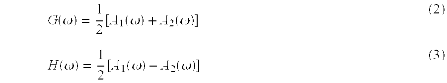
- When both all-pass functions A 1 and A2 have the same phase, G(ω) is maximum and H(ω) is minimum. The phase response determines the location of the poles and the zeros. Additionally, G(ω) and H (ω), are power complementary, since
- |G(ω)|2 +|H(ω)|2=1 (4)
- This sum and difference of the two all-pass functions described above can be implemented in an optical filter using directional couplers as shown in
structure 300 of FIG. 9A. Structure 300 includesdirectional couplers optical paths 303, and all-passoptical filters 304.Directional coupler 301 provides the function of the splitter anddirectional coupler 305 provides the function of the combiner. When the power coupling ratio of eachdirectional coupler equations - All-pass
optical filters 304 suited forstructure 300 can be realized with a ring resonator structure. For example, for an Nth order optical filter having a cascade ring resonator structure, the coupling ratios and the pole locations for each ring are calculated from the transfer function - A(z)|z=e jω =e jφ(ρe −jφ z −1/1−κe jφ z −1) (5)
- wherein the directional coupler bar-state amplitude transmission is designated by ρ={square root}{square root over (1−κ)}, where κ is the coupling ratio of the ring resonator, and φ is a phase associated with one feedback path. The free spectral range (FSR) is given by FSR≅c/(n g2πR), where R is the ring radius, and ng is the effective group index of the fundamental mode. Poles are determined from the root of the denominator of equation (5), while the zeros are determined from the root of the numerator.
- From equation (5), to produce a pole at z n, for the structure shown in FIG. 9B, requires a coupling ratio of κn=1−|Zn|2 and a phase response of φn=arg(zn). The
rings 310 are nominally the same circumference with an incremental length, Δl, or index change, Δn over a length l, added to each ring to realize the phase response, e.g.
- Also, φ tot equals the sum of all e jφn for each all-pass filter. β is a constant determined from adding equations (2) and (3) and evaluating the sum at ω=0.
- Heaters 315 are optionally deposited on a section of the ring, as shown in FIG. 9B, to locally change the index and create the desired phase. These Nth order optical filters require N+2 couplers and N+2 phase shifts, at most. This is in contrast to the general waveguide filter architecture which requires 2N+1 couplers and 2N phase shifters to realize an Nth order filter.
- Another coupled
cavity structure 300 can be realized with reflectors such as Bragg gratings or thin films of alternating high and low refractive index. Such a structure includes one reflector having an amplitude reflectance of unity, i.e. |ρ0|=1. FIG. 9C shows a coupled cavity structure with two all-pass reflective lattice filters 320. Each lattice filter includespartial reflectors 325 and one reflector 322 with 100% reflectivity. The FSR is approximated from FSR=c/(2ng L) where L is the nominal cavity length. The cavity length or index is varied for each stage to create the relative phase φn. In equation (5), the amplitude reflectances are given by ρ. It is desirable for thepartial reflectors 325 to be essentially wavelength independent over the FSR so that the poles and zeros are essentially constant. Thin films with alternating layers of high and low index or Bragg gratings are optionally used to realize the partial reflectors. In either case, the index difference must be large enough to satisfy the wavelength independence constraint. - The channel selector of the present invention is optionally arranged as a concatenated series 350, as shown in FIG. 10. Concatenated series 350 includes three
channel selectors channel selector multi-mode interference coupler 360 and a plurality ofreflective cavities 365. Multi-channel optical signals input to a concatenated series are subjected to two or more channel selections. For example, multi-channel optical signals input to concatenated series 350 are directed tochannel selector 354 where a first channel selection is performed. Thereafter, a portion of the passband selected bychannel selector 354 is directed to channelselectors - The following examples are provided to illustrate specific embodiments of the present invention.
- A channel selector with an 8 th order elliptic optical filter design. The 8th order elliptic filter has a 30 dB stopband rejection for both G(ω) and H(ω) and a cutoff width of about 0.1 x FSR. The stopband rejection requirement of 30 dB H(ω) implies a passband flatness of 0.004 dB for G(ω). The details for determining the filter responses G(ω) and H(ω) as well as all-pass functions A1(ω) and A2(ω) are discussed in Mitra, S et al., “Handbook for Digital Signal Processing”, John Wiley and Sons, N.Y., (1993), which is incorporated herein by reference. The all-pass functions are 4th order functions,

- where D 1(z) and D2(z) are polynomials (D(z)=d0+d1z−1+. . . dnz−n) whose coefficients (dn) are listed in Table 1.
TABLE 1 Dn D1(z) D2(z) d 01 1 d1 −3.4645 − 0.1483i −3.4645 + 0.1483i d2 4.6227 + 0.3638i 4.6227 − 0.3638i d3 −2.8027 − 0.3076i −2.8027 + 0.3076i d4 0.6516 + 0.0864i 0.6516 − 0.0864i - The phase factor β=−1.39492 is given in radians. Given A 1(z) and A2(z), the coupling ratios κ, phases φ, and partial reflectances ρ are determined via equation (5) for the cascade ring and the cavity structure or by step-down recursion relations for the lattice structures (coupled ring or coupled cavity).
- FIG. 11A shows the magnitude response of the 8 th order elliptic filter for the transmission cross and bar states. In FIG. 11A the filter transmission (dB) is plotted as a function of the normalized frequency. The normalized frequency range of 0 to 1 corresponds to one FSR of the frequency response. The graph of FIG. 11A illustrates that in the 8th order design, G(ω) and H(ω) each have a negligible passband transmission rejection and a stopband transmission rejection of 30 dB.
- FIG. 11B is a graph of the magnitude response of the 8 th order elliptic filter having a loss of 0.2 dB/feedback path. The peak passband transmission of G(ω) is reduced, but the 30 dB stopband rejection of G(ω) and H(ω) is retained.
- FIG. 12 depicts a 4×4 channel selector with all-
pass filters 400 positioned on eachoptical path 403 connecting two multi-mode interference (MMI)couplers 405. Eachoptical path 403 has a different path length denoted as 0L, 1L, 2L, and 3L. The all-pass filters 400 in eachoptical path 403 flatten the passband response of the channel selector without increasing the passband loss. FIG. 13A is a graph of the spectral response for the channel selector shown in FIG. 12. In FIG. 13A the frequency response for each output corresponds to H1, H2, H3, and H4. The passband of each output response has a peak transmission range that is flat, denoted as 415 on FIG. 13A. - For comparison purposes a graph of the spectral response of a 4-stage filter without all-pass filters, is shown in FIG. 13B. The peak transmission ranges of H 1, H2, H3, and H4 in FIG. 13B, lack passband flatness when compared to the peak transmission ranges of FIG. 13A. Additionally, the useable width of each band, determined for a stopband rejection of 30 dB, increased from about 6% for the passbands of FIG. 13B to at least 74% for the passbands of FIG. 13A.
- A filter with a linear square magnitude response over a frequency range of 0.15<v<0.85 was designed. The filter is a MZI with a single stage all-pass filter in each arm. The pole magnitudes and phases for the all-pass filters are 0.2925∠0.0088 (radians) and 0.7865∠−0.0099 (radians), respectively. The remaining design parameters are κ=0.5, φ=−0.7121, and 2β=−1.5896 rad. The square magnitude response for this second-order filter is shown in FIG. 14. The square magnitude response is linear to within about ±0.005 over 0.18<v<0.82. Filters with such a square magnitude response are suitable as frequency discriminators for laser wavelength stabilization and modulators which respond linearly to the input signal for analog transmission.
- A
filter 500 having the structure shown in FIG. 15A was designed. Thefilter 500 is aMZI 501 with asingle ring resonator 502 in onearm 515. Eacharm MZI 501 has a specified length (M, N). The ratio (ρ) of the lengths (M, N) of eacharm - A MZI with arm lengths 502 (M=4), 515 (N=3) has the magnitude response shown in FIG. 15B. The transmission response of
arm 502 and thetransmission response 515 include cut-off regions which haveintermediate steps 511. Frequencies which correspond to theintermediate steps 511 are partially transmitted by the filter. Filters with stair-case magnitude responses are suitable as multi-level optical modulators.
Claims (20)
Priority Applications (3)
| Application Number | Priority Date | Filing Date | Title |
|---|---|---|---|
| US09/238,222 US6580534B2 (en) | 1999-01-27 | 1999-01-27 | Optical channel selector |
| EP00300341A EP1024378A2 (en) | 1999-01-27 | 2000-01-19 | Optical channel selector |
| JP2000015649A JP2000267147A (en) | 1999-01-27 | 2000-01-25 | Channel selector for multi-channel optical communication system |
Applications Claiming Priority (1)
| Application Number | Priority Date | Filing Date | Title |
|---|---|---|---|
| US09/238,222 US6580534B2 (en) | 1999-01-27 | 1999-01-27 | Optical channel selector |
Publications (2)
| Publication Number | Publication Date |
|---|---|
| US20020159686A1 true US20020159686A1 (en) | 2002-10-31 |
| US6580534B2 US6580534B2 (en) | 2003-06-17 |
Family
ID=22896986
Family Applications (1)
| Application Number | Title | Priority Date | Filing Date |
|---|---|---|---|
| US09/238,222 Expired - Lifetime US6580534B2 (en) | 1999-01-27 | 1999-01-27 | Optical channel selector |
Country Status (3)
| Country | Link |
|---|---|
| US (1) | US6580534B2 (en) |
| EP (1) | EP1024378A2 (en) |
| JP (1) | JP2000267147A (en) |
Cited By (8)
| Publication number | Priority date | Publication date | Assignee | Title |
|---|---|---|---|---|
| US6574380B2 (en) * | 2000-07-11 | 2003-06-03 | Corning Incorporated | Tapped delay line-based configurable spectral filter with in-situ monitoring |
| US20040042792A1 (en) * | 2002-08-29 | 2004-03-04 | Dean Samara-Rubio | Methods and apparatus for switching N optical input signals to M optical outputs |
| US6788837B2 (en) * | 2001-03-27 | 2004-09-07 | Intel Corporation | Method and apparatus for interleaving and switching an optical beam in a semiconductor substrate |
| US20110280579A1 (en) * | 2010-05-11 | 2011-11-17 | Mclaren Moray | Energy-efficient and fault-tolerant resonator-based modulation and wavelength division multiplexing systems |
| US8355605B1 (en) * | 2008-10-17 | 2013-01-15 | Cirrex Systems Llc | Isolating light paths |
| US20140003810A1 (en) * | 2012-07-02 | 2014-01-02 | Alcatel-Lucent Usa Inc. | Reconfigurable optical networks |
| US20140193155A1 (en) * | 2013-01-10 | 2014-07-10 | The Regents Of The University Of Colorado, A Body Corporate | Microphotonic Coupled-Resonator Devices |
| CN112068248A (en) * | 2020-09-28 | 2020-12-11 | 四川天邑康和通信股份有限公司 | Method for assembling wavelength division multiplexing device |
Families Citing this family (35)
| Publication number | Priority date | Publication date | Assignee | Title |
|---|---|---|---|---|
| US6735368B2 (en) | 1997-05-16 | 2004-05-11 | Mesophotonics Limited | Optical delay device |
| GB9710062D0 (en) | 1997-05-16 | 1997-07-09 | British Tech Group | Optical devices and methods of fabrication thereof |
| US6788863B2 (en) * | 1997-05-16 | 2004-09-07 | Mesophotonics Limited | Optical delay device |
| US6721508B1 (en) | 1998-12-14 | 2004-04-13 | Tellabs Operations Inc. | Optical line terminal arrangement, apparatus and methods |
| US7177550B1 (en) * | 2001-01-24 | 2007-02-13 | Ball Aerospace & Technologies Corp. | On-axis laser receiver wavelength demultiplexer with integral immersion lensed detectors |
| KR100438014B1 (en) * | 2001-08-16 | 2004-06-30 | 주식회사 한빛아이앤씨 | Adaptive optical filters using multi-mode interference |
| US6871022B2 (en) * | 2001-09-14 | 2005-03-22 | Stratos International, Inc. | Cascaded optical multiplexer |
| US6882781B2 (en) * | 2001-11-16 | 2005-04-19 | Hrl Laboratories, Llc | Coherent power combining of single-mode sources in waveguide fiber couplers |
| US7245801B2 (en) * | 2002-03-21 | 2007-07-17 | University Of Rochester | Apparatus with a series of resonator structures situated near an optical waveguide for manipulating optical pulses |
| JP2003337236A (en) | 2002-05-17 | 2003-11-28 | Nec Corp | Optical ring resonator, optical waveguide device and method of manufacturing optical ring resonator |
| US6834141B1 (en) * | 2002-10-22 | 2004-12-21 | Wavesplitter Technologies, Inc. | Wide pass-band interferometric optical device utilizing an optical ring-resonator |
| JP2006278769A (en) * | 2005-03-29 | 2006-10-12 | Nec Corp | Variable wavelength laser |
| US8032027B2 (en) | 2005-07-25 | 2011-10-04 | Massachusetts Institute Of Technology | Wide free-spectral-range, widely tunable and hitless-switchable optical channel add-drop filters |
| US9164239B2 (en) | 2006-03-15 | 2015-10-20 | Alcatel Lucent | Method and apparatus for optically filtering a communication signal |
| US7200299B1 (en) | 2006-03-23 | 2007-04-03 | Lucent Technologies Inc. | Adding and dropping wavelength-channels |
| WO2008008344A2 (en) | 2006-07-11 | 2008-01-17 | Massachusetts Institute Of Technology | Microphotonic maskless lithography |
| US7257291B1 (en) * | 2006-07-29 | 2007-08-14 | Lucent Technologies Inc. | Ultra-narrow bandpass filter |
| WO2008021467A2 (en) | 2006-08-16 | 2008-02-21 | Massachusetts Institute Of Technology | Balanced bypass circulators and folded universally-balanced interferometers |
| WO2008082664A2 (en) | 2006-12-29 | 2008-07-10 | Massachusetts Institute Of Technology | Fabrication-tolerant waveguides and resonators |
| WO2008118465A2 (en) | 2007-03-26 | 2008-10-02 | Massachusetts Institute Of Technology | Hitless tuning and switching of optical resonator amplitude and phase responses |
| US7539375B2 (en) * | 2007-05-04 | 2009-05-26 | Massachusetts Institute Of Technology | Optical coupled resonator structures based on loop-coupled cavities and loop coupling phase |
| US20090003838A1 (en) * | 2007-06-27 | 2009-01-01 | Lucent Technologies Incorporated | Optical Data Communication System Having Reduced Pulse Distortion and Method of Operating the Same |
| US7903909B2 (en) | 2007-10-22 | 2011-03-08 | Massachusetts Institute Of Technology | Low-loss bloch wave guiding in open structures and highly compact efficient waveguide-crossing arrays |
| US8055141B2 (en) | 2007-12-17 | 2011-11-08 | Alcatel Lucent | Balanced optical signal processor |
| US7680362B2 (en) * | 2008-01-15 | 2010-03-16 | Alcatel-Lucent Usa Inc. | CMOS-compatible polarization-diverse tunable optical bandpass filter |
| US7945172B2 (en) * | 2008-05-20 | 2011-05-17 | Harmonic, Inc. | Dispersion compensation circuitry and system for analog video transmission with direct modulated laser |
| JP5315792B2 (en) * | 2008-05-26 | 2013-10-16 | 富士通株式会社 | Light modulator |
| US8032023B2 (en) * | 2008-11-07 | 2011-10-04 | Alcatel Lucent | Reconfigurable DWDM wavelength switch based on complementary bandpass filters |
| US8340478B2 (en) | 2008-12-03 | 2012-12-25 | Massachusetts Institute Of Technology | Resonant optical modulators |
| US8483521B2 (en) | 2009-05-29 | 2013-07-09 | Massachusetts Institute Of Technology | Cavity dynamics compensation in resonant optical modulators |
| IL206143A (en) | 2010-06-02 | 2016-06-30 | Eyal Shekel | Coherent optical amplifier |
| WO2013085820A1 (en) * | 2011-12-09 | 2013-06-13 | Rambus Inc. | Systems and methods for temperature insensitive photonic transmission |
| EP3032303B1 (en) | 2014-12-11 | 2020-06-10 | Alcatel Lucent | Optical device with integrated reflector(s) comprising a loop reflector integrating a mach-zehnder interferometer |
| US20170090267A1 (en) * | 2015-09-30 | 2017-03-30 | Ciena Corporation | Chirp suppressed ring resonator |
| CN108599856B (en) * | 2018-04-02 | 2019-10-25 | 湖北工业大学 | Optical splitter system based on 8 × 1 Mode Coupling receivers |
Citations (6)
| Publication number | Priority date | Publication date | Assignee | Title |
|---|---|---|---|---|
| US5414548A (en) * | 1992-09-29 | 1995-05-09 | Nippon Telegraph And Telephone Corporation | Arrayed-wave guide grating multi/demultiplexer with loop-back optical paths |
| US5471180A (en) * | 1991-02-15 | 1995-11-28 | Lockheed Sanders, Inc. | Low-loss dielectric resonant devices having lattice structures with elongated resonant defects |
| US5523874A (en) * | 1993-01-23 | 1996-06-04 | Northern Telecom Limited | Optical soliton pulse transmission system |
| US5903691A (en) * | 1996-06-24 | 1999-05-11 | Trw Inc. | Optical-loop signal processing using reflection mechanisms |
| US6084992A (en) * | 1997-08-29 | 2000-07-04 | Telefonaktiebolaget Lm Ericsson | Arrangement and method relating to optical transmission |
| US6289151B1 (en) * | 1998-10-30 | 2001-09-11 | Lucent Technologies Inc. | All-pass optical filters |
-
1999
- 1999-01-27 US US09/238,222 patent/US6580534B2/en not_active Expired - Lifetime
-
2000
- 2000-01-19 EP EP00300341A patent/EP1024378A2/en not_active Withdrawn
- 2000-01-25 JP JP2000015649A patent/JP2000267147A/en active Pending
Patent Citations (6)
| Publication number | Priority date | Publication date | Assignee | Title |
|---|---|---|---|---|
| US5471180A (en) * | 1991-02-15 | 1995-11-28 | Lockheed Sanders, Inc. | Low-loss dielectric resonant devices having lattice structures with elongated resonant defects |
| US5414548A (en) * | 1992-09-29 | 1995-05-09 | Nippon Telegraph And Telephone Corporation | Arrayed-wave guide grating multi/demultiplexer with loop-back optical paths |
| US5523874A (en) * | 1993-01-23 | 1996-06-04 | Northern Telecom Limited | Optical soliton pulse transmission system |
| US5903691A (en) * | 1996-06-24 | 1999-05-11 | Trw Inc. | Optical-loop signal processing using reflection mechanisms |
| US6084992A (en) * | 1997-08-29 | 2000-07-04 | Telefonaktiebolaget Lm Ericsson | Arrangement and method relating to optical transmission |
| US6289151B1 (en) * | 1998-10-30 | 2001-09-11 | Lucent Technologies Inc. | All-pass optical filters |
Cited By (14)
| Publication number | Priority date | Publication date | Assignee | Title |
|---|---|---|---|---|
| US6574380B2 (en) * | 2000-07-11 | 2003-06-03 | Corning Incorporated | Tapped delay line-based configurable spectral filter with in-situ monitoring |
| US6788837B2 (en) * | 2001-03-27 | 2004-09-07 | Intel Corporation | Method and apparatus for interleaving and switching an optical beam in a semiconductor substrate |
| US20040218852A1 (en) * | 2001-03-27 | 2004-11-04 | Ansheng Liu | Method and apparatus for interleaving and switching an optical beam a semiconductor substrate |
| US20040042792A1 (en) * | 2002-08-29 | 2004-03-04 | Dean Samara-Rubio | Methods and apparatus for switching N optical input signals to M optical outputs |
| US7242866B2 (en) | 2002-08-29 | 2007-07-10 | Intel Corporation | Methods and apparatus for switching N optical input signals to M optical outputs |
| US8355605B1 (en) * | 2008-10-17 | 2013-01-15 | Cirrex Systems Llc | Isolating light paths |
| US8494311B1 (en) | 2008-10-17 | 2013-07-23 | Michael L. Wach | Isolating light paths |
| US9628187B1 (en) | 2008-10-17 | 2017-04-18 | Michael L. Wach | Isolating light paths |
| US20110280579A1 (en) * | 2010-05-11 | 2011-11-17 | Mclaren Moray | Energy-efficient and fault-tolerant resonator-based modulation and wavelength division multiplexing systems |
| US8705972B2 (en) * | 2010-05-11 | 2014-04-22 | Hewlett-Packard Development Company, L.P. | Energy-efficient and fault-tolerant resonator-based modulation and wavelength division multiplexing systems |
| US20140003810A1 (en) * | 2012-07-02 | 2014-01-02 | Alcatel-Lucent Usa Inc. | Reconfigurable optical networks |
| US9164300B2 (en) | 2012-07-02 | 2015-10-20 | Alcatel Lucent | Reconfigurable optical networks |
| US20140193155A1 (en) * | 2013-01-10 | 2014-07-10 | The Regents Of The University Of Colorado, A Body Corporate | Microphotonic Coupled-Resonator Devices |
| CN112068248A (en) * | 2020-09-28 | 2020-12-11 | 四川天邑康和通信股份有限公司 | Method for assembling wavelength division multiplexing device |
Also Published As
| Publication number | Publication date |
|---|---|
| US6580534B2 (en) | 2003-06-17 |
| JP2000267147A (en) | 2000-09-29 |
| EP1024378A2 (en) | 2000-08-02 |
Similar Documents
| Publication | Publication Date | Title |
|---|---|---|
| US6580534B2 (en) | Optical channel selector | |
| US6289151B1 (en) | All-pass optical filters | |
| Madsen | Efficient architectures for exactly realizing optical filters with optimum bandpass designs | |
| EP1426800B1 (en) | Optical multi/demultiplexing circuit equipped with phase generating device | |
| JP3256418B2 (en) | Optical device | |
| US6839482B2 (en) | Tunable optical filtering device and method | |
| US5309534A (en) | Optical filter having multiple interferometric stages | |
| US6606433B2 (en) | Optical multi/demultiplexer | |
| US20170187483A1 (en) | Low transit loss add-drop multiplexing node for all optical networking | |
| US20020126291A1 (en) | Spectrum division multiplexing for high channel count optical networks | |
| EP1759230A1 (en) | Optical band splitter/combiner and apparatus comprising the same | |
| JP4709694B2 (en) | Chromatic dispersion compensation circuit | |
| US20030128926A1 (en) | Compact wavelength routing device having substantially flat passband | |
| US6236781B1 (en) | Duplicated-port waveguide grating router having substantially flat passbands | |
| Madsen | A multiport frequency band selector with inherently low loss, flat passbands, and low crosstalk | |
| US20030174946A1 (en) | Superstructure photonic band-gap grating add-drop filter | |
| US6907156B1 (en) | Reconfigurable multi-channel filters having enhanced channel bandwidth | |
| JP3681995B2 (en) | Optical multiplexer / demultiplexer | |
| JPH08234149A (en) | Optical filter using electron - optical material | |
| US20030138205A1 (en) | Waveguide grating arrangement using a segmented reflector | |
| KR100237379B1 (en) | Tunable optical drop/pass filter system for wdm | |
| de Ridder et al. | Interleavers | |
| US6907160B2 (en) | Apparatus for filtering optical signals | |
| KR100342533B1 (en) | Tunable optical wavelength demultiplexer and method thereof | |
| Cincotti et al. | Logarithmic wavelength demultiplexers |
Legal Events
| Date | Code | Title | Description |
|---|---|---|---|
| AS | Assignment |
Owner name: LUCENT TECHNOLOGIES INC., NEW JERSEY Free format text: ASSIGNMENT OF ASSIGNORS INTEREST;ASSIGNOR:MADSEN, CHRISTI KAY;REEL/FRAME:009732/0813 Effective date: 19990126 |
|
| FEPP | Fee payment procedure |
Free format text: PAYOR NUMBER ASSIGNED (ORIGINAL EVENT CODE: ASPN); ENTITY STATUS OF PATENT OWNER: LARGE ENTITY |
|
| STCF | Information on status: patent grant |
Free format text: PATENTED CASE |
|
| FPAY | Fee payment |
Year of fee payment: 4 |
|
| FEPP | Fee payment procedure |
Free format text: PAYOR NUMBER ASSIGNED (ORIGINAL EVENT CODE: ASPN); ENTITY STATUS OF PATENT OWNER: LARGE ENTITY Free format text: PAYER NUMBER DE-ASSIGNED (ORIGINAL EVENT CODE: RMPN); ENTITY STATUS OF PATENT OWNER: LARGE ENTITY |
|
| FPAY | Fee payment |
Year of fee payment: 8 |
|
| FPAY | Fee payment |
Year of fee payment: 12 |
|
| AS | Assignment |
Owner name: OMEGA CREDIT OPPORTUNITIES MASTER FUND, LP, NEW YORK Free format text: SECURITY INTEREST;ASSIGNOR:WSOU INVESTMENTS, LLC;REEL/FRAME:043966/0574 Effective date: 20170822 Owner name: OMEGA CREDIT OPPORTUNITIES MASTER FUND, LP, NEW YO Free format text: SECURITY INTEREST;ASSIGNOR:WSOU INVESTMENTS, LLC;REEL/FRAME:043966/0574 Effective date: 20170822 |
|
| AS | Assignment |
Owner name: WSOU INVESTMENTS, LLC, CALIFORNIA Free format text: ASSIGNMENT OF ASSIGNORS INTEREST;ASSIGNOR:ALCATEL LUCENT;REEL/FRAME:044000/0053 Effective date: 20170722 |
|
| AS | Assignment |
Owner name: WSOU INVESTMENTS, LLC, CALIFORNIA Free format text: RELEASE BY SECURED PARTY;ASSIGNOR:OCO OPPORTUNITIES MASTER FUND, L.P. (F/K/A OMEGA CREDIT OPPORTUNITIES MASTER FUND LP;REEL/FRAME:049246/0405 Effective date: 20190516 |
|
| AS | Assignment |
Owner name: OT WSOU TERRIER HOLDINGS, LLC, CALIFORNIA Free format text: SECURITY INTEREST;ASSIGNOR:WSOU INVESTMENTS, LLC;REEL/FRAME:056990/0081 Effective date: 20210528 |