US11966625B2 - Memory device and operating method for setting and repairing data errors - Google Patents
Memory device and operating method for setting and repairing data errors Download PDFInfo
- Publication number
- US11966625B2 US11966625B2 US17/722,850 US202217722850A US11966625B2 US 11966625 B2 US11966625 B2 US 11966625B2 US 202217722850 A US202217722850 A US 202217722850A US 11966625 B2 US11966625 B2 US 11966625B2
- Authority
- US
- United States
- Prior art keywords
- idr
- data
- read
- idr data
- replica
- Prior art date
- Legal status (The legal status is an assumption and is not a legal conclusion. Google has not performed a legal analysis and makes no representation as to the accuracy of the status listed.)
- Active, expires
Links
- 238000011017 operating method Methods 0.000 title claims description 12
- 238000011084 recovery Methods 0.000 claims abstract description 70
- 238000000034 method Methods 0.000 claims description 50
- 238000010586 diagram Methods 0.000 description 17
- 239000010410 layer Substances 0.000 description 15
- 101100481702 Arabidopsis thaliana TMK1 gene Proteins 0.000 description 12
- 238000004519 manufacturing process Methods 0.000 description 10
- 230000006866 deterioration Effects 0.000 description 8
- 239000000758 substrate Substances 0.000 description 7
- 230000014759 maintenance of location Effects 0.000 description 6
- 238000003860 storage Methods 0.000 description 6
- 238000009826 distribution Methods 0.000 description 5
- 101100481704 Arabidopsis thaliana TMK3 gene Proteins 0.000 description 3
- 238000005516 engineering process Methods 0.000 description 3
- 230000002093 peripheral effect Effects 0.000 description 3
- VYPSYNLAJGMNEJ-UHFFFAOYSA-N Silicium dioxide Chemical compound O=[Si]=O VYPSYNLAJGMNEJ-UHFFFAOYSA-N 0.000 description 2
- 230000007423 decrease Effects 0.000 description 2
- 238000001514 detection method Methods 0.000 description 2
- 239000012535 impurity Substances 0.000 description 2
- 239000011810 insulating material Substances 0.000 description 2
- 230000004044 response Effects 0.000 description 2
- 229910052814 silicon oxide Inorganic materials 0.000 description 2
- 239000002210 silicon-based material Substances 0.000 description 2
- 238000004566 IR spectroscopy Methods 0.000 description 1
- 230000000903 blocking effect Effects 0.000 description 1
- 230000002939 deleterious effect Effects 0.000 description 1
- 230000006870 function Effects 0.000 description 1
- 238000010348 incorporation Methods 0.000 description 1
- 238000013507 mapping Methods 0.000 description 1
- 230000000149 penetrating effect Effects 0.000 description 1
- 239000007787 solid Substances 0.000 description 1
- 239000002344 surface layer Substances 0.000 description 1
- 230000005641 tunneling Effects 0.000 description 1
Images


Classifications
-
- G—PHYSICS
- G11—INFORMATION STORAGE
- G11C—STATIC STORES
- G11C16/00—Erasable programmable read-only memories
- G11C16/02—Erasable programmable read-only memories electrically programmable
- G11C16/06—Auxiliary circuits, e.g. for writing into memory
- G11C16/26—Sensing or reading circuits; Data output circuits
-
- G—PHYSICS
- G11—INFORMATION STORAGE
- G11C—STATIC STORES
- G11C16/00—Erasable programmable read-only memories
- G11C16/02—Erasable programmable read-only memories electrically programmable
- G11C16/06—Auxiliary circuits, e.g. for writing into memory
- G11C16/10—Programming or data input circuits
- G11C16/20—Initialising; Data preset; Chip identification
-
- G—PHYSICS
- G06—COMPUTING; CALCULATING OR COUNTING
- G06F—ELECTRIC DIGITAL DATA PROCESSING
- G06F3/00—Input arrangements for transferring data to be processed into a form capable of being handled by the computer; Output arrangements for transferring data from processing unit to output unit, e.g. interface arrangements
- G06F3/06—Digital input from, or digital output to, record carriers, e.g. RAID, emulated record carriers or networked record carriers
- G06F3/0601—Interfaces specially adapted for storage systems
- G06F3/0628—Interfaces specially adapted for storage systems making use of a particular technique
- G06F3/0655—Vertical data movement, i.e. input-output transfer; data movement between one or more hosts and one or more storage devices
-
- G—PHYSICS
- G06—COMPUTING; CALCULATING OR COUNTING
- G06F—ELECTRIC DIGITAL DATA PROCESSING
- G06F11/00—Error detection; Error correction; Monitoring
- G06F11/07—Responding to the occurrence of a fault, e.g. fault tolerance
- G06F11/08—Error detection or correction by redundancy in data representation, e.g. by using checking codes
- G06F11/10—Adding special bits or symbols to the coded information, e.g. parity check, casting out 9's or 11's
- G06F11/1008—Adding special bits or symbols to the coded information, e.g. parity check, casting out 9's or 11's in individual solid state devices
- G06F11/1068—Adding special bits or symbols to the coded information, e.g. parity check, casting out 9's or 11's in individual solid state devices in sector programmable memories, e.g. flash disk
-
- G—PHYSICS
- G06—COMPUTING; CALCULATING OR COUNTING
- G06F—ELECTRIC DIGITAL DATA PROCESSING
- G06F3/00—Input arrangements for transferring data to be processed into a form capable of being handled by the computer; Output arrangements for transferring data from processing unit to output unit, e.g. interface arrangements
- G06F3/06—Digital input from, or digital output to, record carriers, e.g. RAID, emulated record carriers or networked record carriers
- G06F3/0601—Interfaces specially adapted for storage systems
- G06F3/0602—Interfaces specially adapted for storage systems specifically adapted to achieve a particular effect
- G06F3/0604—Improving or facilitating administration, e.g. storage management
-
- G—PHYSICS
- G06—COMPUTING; CALCULATING OR COUNTING
- G06F—ELECTRIC DIGITAL DATA PROCESSING
- G06F3/00—Input arrangements for transferring data to be processed into a form capable of being handled by the computer; Output arrangements for transferring data from processing unit to output unit, e.g. interface arrangements
- G06F3/06—Digital input from, or digital output to, record carriers, e.g. RAID, emulated record carriers or networked record carriers
- G06F3/0601—Interfaces specially adapted for storage systems
- G06F3/0668—Interfaces specially adapted for storage systems adopting a particular infrastructure
- G06F3/0671—In-line storage system
- G06F3/0673—Single storage device
- G06F3/0679—Non-volatile semiconductor memory device, e.g. flash memory, one time programmable memory [OTP]
-
- G—PHYSICS
- G11—INFORMATION STORAGE
- G11C—STATIC STORES
- G11C29/00—Checking stores for correct operation ; Subsequent repair; Testing stores during standby or offline operation
- G11C29/52—Protection of memory contents; Detection of errors in memory contents
-
- G—PHYSICS
- G11—INFORMATION STORAGE
- G11C—STATIC STORES
- G11C16/00—Erasable programmable read-only memories
- G11C16/02—Erasable programmable read-only memories electrically programmable
- G11C16/04—Erasable programmable read-only memories electrically programmable using variable threshold transistors, e.g. FAMOS
- G11C16/0483—Erasable programmable read-only memories electrically programmable using variable threshold transistors, e.g. FAMOS comprising cells having several storage transistors connected in series
-
- G—PHYSICS
- G11—INFORMATION STORAGE
- G11C—STATIC STORES
- G11C16/00—Erasable programmable read-only memories
- G11C16/02—Erasable programmable read-only memories electrically programmable
- G11C16/06—Auxiliary circuits, e.g. for writing into memory
- G11C16/10—Programming or data input circuits
Definitions
- Embodiments relate to a memory device, and more particularly, to a memory device improving the reliability of setting data and an operating method thereof.
- a non-volatile memory device includes a plurality of memory cells that store data in a non-volatile manner.
- a flash memory device may be used in portable phones, digital cameras, portable digital assistants (PDAs), mobile computing devices, stationary computing devices, and other devices.
- a memory device includes a cell array including a plurality of cell blocks, each cell block including a plurality of pages, and a control logic configured to control a program and read operation on the cell array, wherein at least one page of the cell array stores information data read (IDR) data including information related to a setting operation of the memory device, at least another page of the cell array stores replica IDR data including inverted bit values of the IDR data, and the control logic is configured to, when read fail of the IDR data occurs, control a recovery operation for repairing errors in the IDR data by reading the replica IDR data.
- IDR information data read
- a memory device includes a cell array including a plurality of cell blocks, each including a plurality of pages, and a control logic configured to control a program and read operation on the cell array, wherein the cell array stores first to Nth IDR data pairs, each of the first to Nth IDR data pairs includes IDR data including information related to a setting operation of the memory device and replica IDR data including inverted bit values of the IDR data, and the control logic is configured to perform a recovery operation for repairing errors in the IDR data based on at least one IDR data pair among the first to Nth IDR data pairs.
- An operating method of a memory device includes reading, from a cell array of the memory device, IDR data including information related to a setting operation of the memory device, determining whether read fail of the read IDR data occurs, when the read fail occurs in the read IDR data, reading, from the cell array, replica IDR data including inverted bit values with respect to the IDR data, and performing a recovery operation for repairing errors in the IDR data by using the read replica IDR data.
- FIG. 1 is a block diagram illustrating a memory system according to an example embodiment
- FIGS. 2 A and 2 B are diagrams illustrating an example of storing information data read (IDR) data and replica IDR data;
- FIG. 3 is a block diagram illustrating an example embodiment of a controller included in a memory system
- FIG. 4 is a perspective view illustrating an example embodiment of a cell block of a memory device
- FIG. 5 is a block diagram illustrating a memory device according to an example embodiment
- FIG. 6 is a diagram illustrating an example of IDR data deterioration that may occur in a process of manufacturing a memory device
- FIG. 7 is a flowchart illustrating an operating method of a memory system, according to an example embodiment
- FIG. 8 shows an example of a threshold voltage distribution of memory cells in which IDR data and replica IDR data are stored
- FIG. 9 is a flowchart illustrating an example of data determination according to a majority rule, according to example embodiments.
- FIG. 10 is a diagram illustrating an example in which a result of reading an IDR data pair is stored in latches, according to an example embodiment
- FIGS. 11 and 12 are diagrams illustrating examples of performing a majority rule while changing a read level according to example embodiments
- FIG. 13 is a diagram illustrating an example of determining bit values of IDR data, according to example embodiments.
- FIG. 14 is a block diagram illustrating an example in which a memory device is applied to a solid-state drive (SSD) system, according to example embodiments.
- SSD solid-state drive
- FIG. 1 is a block diagram illustrating a memory system 10 according to an example embodiment.
- the memory system 10 may include a memory controller 100 and a memory device 200 .
- the memory controller 100 may include a processor 110 and a setting control module 120 .
- the memory device 200 may include a cell array 210 , a page buffer 220 , and a control logic 230 .
- the memory device 200 may include a non-volatile memory device.
- the memory device 200 may include a non-volatile memory device such as NAND flash memory, vertical NAND flash memory, NOR flash memory, resistive random access memory, phase-change memory, magnetoresistive random access memory, or the like.
- the memory device 200 or the memory system 10 may be implemented as an embedded memory embedded in an electronic device, or as an external memory detachable from the electronic device.
- the memory device 200 or the memory system 10 may be implemented in various forms such as an embedded universal flash storage (UFS) memory device, an embedded multi-media card (eMMC), a solid state drive (SSD), a UFS memory card, a CompactFlash (CF) card, a Secure Digital (SD) card, a micro-SD card, a mini-SD, extreme digital (xD) card, a memory stick, and the like.
- UFS embedded universal flash storage
- eMMC embedded multi-media card
- SSD solid state drive
- CF CompactFlash
- SD Secure Digital
- micro-SD card micro-SD card
- mini-SD mini-SD
- extreme digital (xD) card extreme digital
- the memory controller 100 may control the memory device 200 to read data that is stored in the memory device 200 or to write (or program) data to the memory device 200 , in response to a write/read request from a host HOST.
- the memory controller 100 may control program, read, and erase operations of the memory device 200 by providing an address ADD and a command CMD to the memory device 200 . Also, data DATA to be written to the memory device 200 and data DATA read from the memory device 200 may be transmitted and received between the memory controller 100 and the memory device 200 . Also, information data read (IDR) data may be read from the memory device 200 .
- IDR information data read
- the cell array 210 may include a plurality of cell regions 211 _ 1 to 211 _N (also respectively referred to as a first cell region 211 _ 1 to an Nth cell region 211 _N).
- each of the plurality of cell regions 211 _ 1 to 211 _N may have a certain unit, and for example, each of the plurality of cell regions 211 _ 1 to 211 _N may be referred to as a cell block or a plane.
- each of the plurality of cell regions 211 _ 1 to 211 _N may include a plurality of pages, and each of the pages may include a plurality of memory cells.
- a data erase operation may be performed in units of cell blocks, and data program and read operations may be performed in units of pages.
- At least some of the plurality of cell regions 211 _ 1 to 211 _N may store main data such as setting data related to an operating condition of the memory system 10 .
- FIG. 1 illustrates that all of the plurality of cell regions 211 _ 1 to 211 _N store setting data (IDR), the setting data may be stored only in some cell regions.
- IDR setting data
- a process of reading setting data (e.g., DR data) that is set or stored in the non-volatile memory device, and setting various operating conditions of the memory system based on the setting data that is read, may be performed.
- the setting data e.g., DR data
- the non-volatile memory device e.g., the memory device 200
- main information related to operation of the memory system e.g., the memory system 10
- it is important to ensure reliability in the process of reading of the setting data e.g., the DR data.
- the memory device 200 may store setting data in the form of information data read (DR) data (which may be referred to herein as IDR data, and indicated in the drawings as DR).
- IDR data is used to set an initial operating condition, e.g., in an initial driving process of the memory system 10 .
- the IDR data may include DC information, option information, repair information, and bad block information, which are used for initialization of the memory system 10 .
- the memory device 200 may be a non-volatile memory device that has stored therein or set therein the IDR data during manufacture of the memory device 200 , e.g., prior to completion of manufacturing of a component or system that includes the memory device 200 .
- the IDR data is stored or set in the memory device 200 (e.g., in at least some of the plurality of cell regions 211 _ 1 to 211 _N) during the process of manufacturing.
- the IDR data may be stored in the memory device 200 prior to mounting the memory device 200 on a board such as a PCB.
- the memory device 200 may be exposed to very high temperatures and the internal temperature of the memory device 200 may become significantly elevated. Such elevated temperatures may have deleterious effects on data retention characteristics of the memory cells storing the IDR data, such that the IDR data stored in the memory device 200 may be deteriorated, e.g., loss or corruption of one or more bits of stored IDR data may occur. Additional aspects of the IDR data and its use and incorporation in a memory device are set forth in U.S. Pat. No. 11,003,393 B2 and 11,056,200 B2, which are hereby incorporated by reference in their entireties for all purposes.
- an operation of reading the IDR data in order to sett an operating environment or an operating condition, a recovery operation for repairing errors in IDR data, and setting operations using IDR data and/or repaired IDR data may be performed in series.
- the various operations as described above may be performed by the memory controller 100 and/or the memory device 200 .
- the operation of the reading of the IDR data and the recovery operation are described as being performed by the memory device 200
- the setting operations is described as being performed by the memory controller 100 .
- this may be varied, and the memory system 10 may be implemented in such a manner that the operations described above are distributed to the memory controller 100 and the memory device 200 according to various methods.
- information storage and recovery operations according to an example embodiment are applied to the setting data is described, but example embodiments are not limited thereto and may be applied to other various types of main data.
- the IDR data may be information stored during a process of manufacturing the memory system 10 or the memory device 200 .
- a cell region in which the IDR data is stored may include a single level cell (SLC) structure, whereas a cell region in which user data is stored may store two or more bits of information in one memory cell, e.g., a multi-level cell (MLC) structure.
- a particular cell region may store only the IDR data, or the memory system 10 may be operated in such a manner that the IDR data and the user data are stored together in a shared cell region.
- the processor 110 may control overall operations of the memory controller 100 .
- the processor 110 may execute an instruction stored in the memory controller 100 to control an operation of the memory controller 100 or control various operations related to data erase/program/read.
- the setting control module 120 may set various operating conditions of the memory device 200 based on the IDR data provided from the memory device 200 .
- the memory device 200 may repair errors in the IDR data that is read from the cell array 210 , and provide the repaired IDR data to the memory controller 100 .
- the control logic 230 may include an IDR recovery module 231 that controls a recovery operation for repairing errors in IDR data.
- each of the setting control module 120 and the IDR recovery module 231 may be implemented as hardware or software, or may be implemented as a combination of hardware and software.
- the setting control module 120 and the IDR recovery module 231 may be respectively referred to as a setting control circuit and an IDR recovery circuit.
- the setting control module 120 and the IDR recovery module 231 may be loaded and executed in a memory (not shown) provided in each of the memory controller 100 and the memory device 200 .
- the control logic 230 may control overall operations of the memory device 200 in relation to a memory operation. For example, the control logic 230 may generate an internal control signal for an internal control operation of the memory device 200 based on a control signal (not shown) from the memory controller 100 .
- the IDR data may be stored in the cell array 210 .
- replica IDR data (which may be referred to herein as replica IDR data, and indicated in the drawings as RIDR) corresponding to the IDR data may be stored in the cell array 210 , and may be used to improve the reliability of the IDR data.
- the data are stored before the product is shipped, and in particular, the data are stored at a predetermined location within the memory (e.g., a cell block at a specific location).
- the replica IDR data and the IDR data may be stored in different pages of an identical cell block.
- the replica IDR data and the IDR data may be stored in different cell blocks.
- the IDR data may include a plurality of bits, and replica IDR data having inverted values of the plurality of bits may be stored in the cell array 210 .
- the IDR data and the replica IDR data may be defined as constituting an IDR data pair, which may be referred to herein and indicated in the drawings as IDR_P, e.g., IDR_P 1 , IDR_P 2 , . . . , IDR_PM).
- IDR data corresponding to original data may be stored in one cell region, and based on the original data, data copied to the plurality of cell regions 211 _ 1 to 211 _N may also be defined as replica IDR data.
- data having bit values equal to those of the original data may be defined as replica IDR data, and data having inverted bit values with respect to the original data may be defined as inverted replica IDR data.
- IDR data information having bit values equal to those of original data stored in the cell array 210
- replica IDR data information having inverted bit values of the original data
- the control logic 230 may receive the IDR data stored in the first cell region 211 _ 1 through the page buffer 220 and determine whether a read fail of the IDR data occurs. If errors or uncorrectable errors occur in the IDR data, the read fail of the IDR data may be determined, and a series of operations for a recovery operation may be controlled.
- control logic 230 may read one or more IDR data pairs IDR_P stored in the cell array 210 , and based on the one or more IDR data pairs IDR_P, perform a recovery operation. For example, replica IDR data stored in the first cell region 211 _ 1 may be read, whether a read fail of the read replica IDR data occurs may be determined, and when the read fail of the replica IDR data does not occur, inverted bit values of the replica IDR data may be used as IDR data.
- a plurality of IDR data pairs IDR_P stored in the cell array 210 may be read, a plurality of bit values related to respective bits of IDR data may be determined from the plurality of IDR data pairs IDR_P, and, by applying a majority rule with respect to the plurality of determined bit values, each of the bit values (or logic states) of the IDR data may be determined. Aspects of these operations will now be described in additional detail.
- FIGS. 2 A and 2 B a detailed example of storing IDR data and replica IDR data according to an example embodiment is described as follows.
- FIGS. 2 A and 2 B show, by way of example, a case in which one piece of IDR data is stored, as original data, in one page of a cell region, but IDR data may be stored in a plurality of pages or may be stored in a plurality of cell regions. Also, in FIGS. 2 A and 2 B , a cell block is exemplified as a cell region in which IDR data is stored.
- a cell array may include first to Nth cell blocks BLK 1 to BLKN as a plurality of cell regions.
- an IDR data pair may be stored in at least some of the first to Nth cell blocks BLK 1 to BLKN in relation to setting an operating condition of a memory system including the memory device.
- some of the first to Nth cell blocks BLK 1 to BLKN store setting data, others store user data, and first to Mth IDR data pairs IDR_P (e.g., IDR_P 1 to IDR_PM) are stored in the cell array 210 as setting data.
- IDR data corresponding to original data may be stored in one page of the first cell block BLK 1 .
- Replica IDR data (which may be generated by performing a NOT operation on the IDR data) may be stored in another page of the first cell block BLK 1 .
- the IDR data and the replica IDR data may constitute the first IDR data pair IDR_P 1 .
- additional IDR data pairs may be further stored in one or more cell blocks.
- the second to Mth IDR data pairs IDR_P 2 to IDR_PM are further stored in the first cell block BLK 1 and the second cell block BLK 2 .
- IDR data corresponding to original data may be copied to the first cell block BLK 1 and the second cell block BLK 2
- replica IDR data having inverted values of bits of the original data may be copied to the first cell block BLK 1 and the second cell block BLK 2 .
- setting data is stored together with user data in at least some of the first to Nth cell blocks BLK 1 to BLKN, and for example, the first to Mth IDR data pairs IDR_P 1 to IDR_PM based on IDR data corresponding to original data may be stored in the first to Nth cell blocks BLK 1 to BLKN.
- user data may be stored in a region in which setting data is not stored.
- one bit may be stored in each of memory cells of a region in which setting data is stored, whereas two or more bits may be stored in each of memory cells of a region in which user data is stored.
- IDR data stored in the first cell block BLK 1 may be read, and whether a read fail of the read IDR data occurs may be determined. For example, whether a read fail occurs may be determined according to whether errors in the IDR data read from the first cell block BLK 1 are correctable, and when it is determined that read fail has occurred, a recovery operation may be performed by reading replica IDR data of the first IDR data pair IDR_P 1 , or a recovery operation may be performed by reading one or more other IDR data pairs.
- a recovery operation may be performed based on replica IDR data including inverted bit values of the IDR data as described above, a bit in which errors have occurred in a process of reading the IDR data and a bit in which errors have occurred in a process of reading the replica IDR data may be of different positions, and thus, the number of bits in which errors occur in all processes of the reading described above may be reduced or minimized.
- replica IDR data includes inverted bit values with respect to IDR data
- bits in which errors occur in all processes of reading the IDR data and the replica IDR data may be minimized, and a recovery operation based on a plurality of IDR data pairs each including original data and replica IDR data having the inverted bit values may be performed, and thus, the possibility of success of the recovery operation may be improved.
- replica IDR data of the first IDR data pair IDR_P 1 may be read, and the second to Mth IDR data pairs IDR_P 2 to IDR_PM may be read.
- the errors of the bits may be repaired based on at least some of the first to Mth IDR data pairs IDR_P 1 to IDR_PM that have been read through the above process, and for example, the errors may be repaired based on a majority rule using bit values determined from a plurality of IDR data pairs.
- replica IDR data of the first IDR data pair IDR_P 1 may be read, and whether a read fail of the read replica IDR data occurs may be determined. If the read fail of the replica IDR data does not occur, inverted bit values of the replica IDR data may be used as the IDR data. In contrast, when the read fail of the replica IDR data occurs, a recovery operation based on the majority rule may be performed.
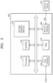
- FIG. 3 is a block diagram illustrating an example embodiment of a controller included in a memory system.
- a memory controller 300 may include a processor 310 , a setting control module 320 , a buffer 330 , random access memory (RAM) 340 , a host interface 350 , and a memory interface 360 .
- the processor 310 may be electrically connected to various components in the memory controller 300 through a bus, and may perform a control operation thereon.
- the processor 310 may control a memory device 301 to perform a memory operation in response to a request received from a host HOST. Also, the processor 310 may perform overall control operations of a memory system by executing instructions stored in the RAM 340 . For example, mapping information used to convert a logical address into a physical address of the memory device 301 may be stored in the RAM 340 . In the buffer 330 , write data transmitted from the host HOST may be temporarily stored or read data read from the memory device 301 may be temporarily stored.
- the host interface 350 may communicate with the host HOST according to a certain interface.
- the host interface 350 may include, for example, an advanced technology attachment (ATA) interface, a serial advanced technology attachment (SATA) interface, a parallel advanced technology attachment (PATA) interface, a universal serial bus (USB) or serial attached small computer system (SAS) interface, a small computer system interface (SCSI), an embedded multi-media card (eMMC) interface, and a Unix file system (UFS) interface, etc.
- ATA advanced technology attachment
- SATA serial advanced technology attachment
- PATA parallel advanced technology attachment
- USB universal serial bus
- SAS serial attached small computer system
- SCSI small computer system interface
- eMMC embedded multi-media card
- UFS Unix file system
- the memory interface 360 may be electrically connected to the memory device 301 , and may receive, from the memory device 301 , the IDR data according to an example embodiment.
- the setting control module 320 may set various operating conditions of the memory device 301 based on IDR data according to example embodiments.
- the setting control module 320 may be implemented by firmware including one or more instructions, and the instructions included in the setting control module 320 may be loaded into the RAM 340 .
- FIG. 4 is a perspective view illustrating an example embodiment of a cell block of a memory device.
- a cell block BLK is formed in a direction perpendicular to a substrate SUB.
- the substrate SUB has a first conductivity type (for example, a p type), and a common source line CSL extending in a second horizontal direction HD 2 on the substrate SUB and doped with impurities of a second conductivity type (for example, an n type) may be provided.
- a plurality of insulating layers IL extending in the second horizontal direction HD 2 are sequentially provided in a vertical direction VD in a region of the substrate SUB between two neighboring common source lines CSL, and the plurality of insulating layers IL are apart from each other by a specific distance in the vertical direction VD.
- the plurality of insulating layers IL may include an insulating material such as silicon oxide.
- a plurality of pillars P sequentially arranged in a first horizontal direction HD 1 and penetrating the plurality of insulating layers IL in the vertical direction VD are provided in a region of the substrate SUB between two neighboring common source lines CSL.
- the plurality of pillars P may penetrate the plurality of insulating layers IL and contact the substrate SUB.
- a surface layer S of each of the pillars P may include a silicon material having a first type and may function as a channel region.
- an inner layer I of each of the pillars P may include an insulating material such as silicon oxide or an air gap.
- a charge storage layer CS is provided along exposed surfaces of the insulating layers IL, the pillars P, and the substrate SUB.
- the charge storage layer CS may include a gate insulating layer (also referred to as a “tunneling insulating layer”), a charge trap layer, and a blocking insulating layer.
- the charge storage layer CS may have an oxide-nitride-oxide (ONO) structure.
- a gate electrode GE such as select lines GSL and SSL and word lines WL 0 to WL 7 is provided on an exposed surface of the charge storage layer CS in a region between two neighboring common source lines CSL.
- Drains or drain contacts DR are respectively provided on the plurality of pillars P.
- drains or drain contacts DR may include a silicon material doped with impurities having a second conductivity type.
- Bit lines BL 1 to BL 2 extending in the first horizontal direction HD 1 and spaced apart from each other by a specific distance in the second horizontal direction HD 2 are provided on the drains or drain contacts DR.
- FIG. 5 is a block diagram illustrating a memory device according to an example embodiment.
- a memory device 400 may include a cell array 410 and a peripheral circuit 420 , and the peripheral circuit 420 may include a page buffer 421 , a control logic 422 , a voltage generator 423 , and a row decoder 424 .
- the peripheral circuit 420 may further include various components such as a data input/output circuit or an input/output interface.
- the cell array 410 may be connected to the page buffer 421 through a plurality of bit lines BL, and may be connected to the row decoder 424 through word lines WL, string select lines SSL, and ground select lines GSL.
- the cell array 410 may include a plurality of memory cells, and for example, the memory cells may be flash memory cells.
- the cell array 410 may store the plurality of IDR data pairs IDR_P according to example embodiments.
- the control logic 422 may program data in the cell array 410 based on a command CMD, an address ADD, and a control signal CTRL, and may output various control signals for reading the data from the cell array 410 , for example, a voltage control signal CTRL_vol, a row address X-ADD, and a column address Y-ADD.
- control logic 422 may include an IDR recovery module 422 _ 1 that recovers IDR data based on IDR data pairs IDR_P.
- the voltage generator 423 may generate various types of voltages for performing program, read, and erase operations on the cell array 410 based on the voltage control signal CTRL_vol.
- the voltage generator 423 may generate a word line voltage VWL, for example, a program voltage, a read voltage, and an erase voltage.
- the voltage generator 423 may further generate a string select line voltage and a ground select line voltage based on the voltage control signal CTRL_vol.
- the page buffer 421 may be connected to a page of the cell array 410 through the plurality of bit lines BL.
- the page buffer 421 may include one or more latches for storing data corresponding to a page, and for example, the page buffer 421 may include first to Kth latches.
- each of the first to Kth latches may store data of one page of the cell array 410
- IDR data in the IDR data pair IDR_P may be stored in one latch
- replica IDR data may be stored in another latch.
- IDR data when IDR data is read and stored in the first latch and replica IDR data is read, the IDR data stored in the first latch shifts to the second latch, and the replica IDR data read from the cell array 410 may be stored in the first latch.
- the IDR recovery module 422 _ 1 may control a recovery operation based on a plurality of IDR data pairs IDR_P read from the cell array 410 . For example, regarding a recovery operation of IDR data, an operation of reading one or more IDR data pairs IDR_P and an operation of determining bit values of the one or more read IDR data pairs IDR_P may be performed based on the control by the IDR recovery module 422 _ 1 .
- the IDR recovery module 422 _ 1 may control recovery IDR data, which constitutes an IDR data pair identical to the read IDR data, to be read, determine whether a read fail of the read recovery IDR data occurs, and as a result of the determining, perform recovery based on the read recovery IDR data.
- the IDR recovery module 422 _ 1 may control a plurality of IDR data pairs IDR_P to be read, and perform recovery based on a majority rule for each of bit values of the plurality of read IDR data pairs IDR_P.
- FIG. 6 is a diagram illustrating an example of IDR data deterioration that may occur in a process of manufacturing a memory device.
- extremely high-temperature heat may be applied to the memory device, and in this case, retention characteristics of IDR data stored in the memory device may be deteriorated.
- high-temperature infrared rays IR may be applied to the memory device several times or higher-temperature heat (approximately 400 degrees Celsius is illustrated) may be applied to the memory device, and in this case, due to charge leakage of memory cells in which the IDR data is programmed, a phenomenon in which distribution is shifted to reduce a threshold voltage thereof may occur.
- deterioration as shown in FIG. 6 may occur, and data of at least some of memory cells programmed to have a relatively high threshold voltage level may be lost.
- the plurality of pieces of IDR data may have the same deterioration characteristics, and thus, when retention characteristics are deteriorated due to the high heat as described above, simultaneous errors may occur in specific bits of the IDR data, and the possibility that the errors are unrepairable may increase.
- replica IDR data obtained by inverting bit values of IDR data is stored in the memory device, and the possibility that errors occur in the same bits in a process of reading the IDR data and the replica IDR data may be reduced, and thus, the probability of success of a recovery operation for repairing errors in the IDR data may be improved.
- FIG. 7 is a flowchart illustrating an operating method of a memory system, according to an example embodiment.
- an IDR process for reading IDR data that is pre-stored in the memory device may be started (operation S 11 ).
- the IDR data may be read as setting data stored in a cell array (operation S 12 ).
- the read IDR data may be original data including a plurality of bits stored in one or more pages, and a plurality of pieces of IDR data including bit values equal to those of the original data and a plurality of pieces of replica IDR data including inverted bit values with respect to the original data may be copied to the cell array.
- An error detection operation may be performed on the read IDR data, and whether a read fail of the IDR data occurs may be determined based on error detection (operation S 13 ). If it is determined that reading of the IDR data is successful because there is no error or only correctable errors in the read IDR data, an initialization operation such as setting an operating condition of a memory system by using the read IDR data may be performed (operation S 14 ).
- a process of reading one or more IDR data pairs IDR_P may be performed (operation S 15 ).
- one or more IDR data pairs IDR_P including IDR data and replica IDR data may be read, and an IDR recovery operation may be performed using the one or more read IDR data pairs IDR_P (operation S 16 ).
- the IDR data and the replica IDR data which have different bit values, are used for the IDR recovery operation, the probability that errors overlappingly occur with respect to the same bits may be reduced, and whether recovery is successful may be determined based on whether all bits of the IDR data may be determined (operation S 17 ). If the recovery fails because some bits of the IDR data are not determined even in the IDR recovery operation, IDR read fail may be finally determined (operation S 18 ).
- a case where it is determined that the recovery is successful in the IDR recovery operation indicates a case where the bit values of the original IDR data may be determined, and thus, an operation of setting an operating condition for the memory system by using the IDR data in which errors are repaired may be performed (operation S 19 ).
- FIG. 8 shows an example of a threshold voltage distribution of memory cells in which IDR data and replica IDR data are stored.
- each of a plurality of bits of the IDR data may have a bit value of “1” or “0”, and it may be determined that, among a plurality of memory cells in which the IDR data is stored, based on a certain read level, an on cell (or memory cells having a relatively small threshold voltage) has a bit value of “1” and an off cell has a bit value of “0”.
- information obtained by inverting bit values read from memory cells may be stored in a page buffer, and thus, based on the certain read level, information having a bit value of “0” corresponding to the on cell may be stored in the page buffer, whereas information having a bit value of “1” corresponding to the off cell may be stored in the page buffer.
- some memory cells may be determined as on cells despite being programmed as off cells in a process of reading the IDR data, and memory cells programmed as off cells may be erroneously determined as on cells even in a process of reading the replica IDR data.
- a bit value “0” may be erroneously determined as a bit value “1”
- a bit value “1” may be erroneously determined as a bit value “0”.
- bit values of memory cells determined as on cells in both of the process of the reading of the IDR data and the process of the reading of the replica DR data may correspond to “1” or “0”, thereby indicating a case where the bit values are not determined.
- bit values of some of the memory cells determined as on cells in both of the process of the reading of the IDR data and the process of the reading of the replica DR data are normally read as “0”, whereas bit values of others may be erroneously read as “0” even though a normal bit value corresponds to “1”.
- bit values of memory cells determined as off cells may be determined as “0”, and in the process of the reading of the replica IDR data, bit values of memory cells determined as off cells may be determined as “1”.
- off cells are degraded to on cells based on a certain read level, and thus, it is assumed that there is no case where memory cells are determined as off cells in both of the process of the reading of the DR data and the process of the reading of the replica IDR data.
- bit value determination operation for at least one other IDR data pair (referred to as a plurality of second IDR data pairs) may be performed.
- bit values may be determined by a read and determination operation for the plurality of second IDR data pairs.
- a value of a specific bit may be determined as “1” or “0” based on the plurality of second DR data pairs, and the value of the specific bit may be determined as one of “1” and “0” based on a majority rule.
- a case where a bit value of data is not determined may correspond to a case where memory cells are determined as on cells in both of a process of reading DR data and a process of reading replica DR data, and thus, a precharge operation may be selectively performed on only some of bit lines in the process of the reading of the replica DR data. For example, as precharge may not be performed on bit lines connected to memory cells determined as off cells in a process of reading DR data, a read operation may not be performed on the memory cells connected to the bit lines on which the precharge is not performed in a process of reading replica IDR data.
- FIG. 9 is a flowchart illustrating an example of data determination according to a majority rule, according to example embodiments.
- DR data stored in one or more pages of a memory device may be read in a process of initializing a memory system (operation S 21 ).
- Whether all bits of the read DR data are determined may be determined (operation S 22 ). If, as a result of the determining, values of all bits of the DR data are normally determined, an initialization operation such as setting an operating condition of the memory system by using the read IDR data may be performed (operation S 23 ).
- a read operation may be performed on replica IDR data stored in the memory device, and for example, one or more DR data pairs each including DR data and replica IDR data may be read.
- first to Nth DR data pairs IDR_P are read, in which N may be an integer of 2 or more (operation S 24 ), and in an example embodiment, as a first IDR data pair includes the read IDR data, the first IDR data pair may be configured by reading only replica IDR data.
- a recovery operation may be performed based on the read first to Nth IDR data pairs IDR_P, and thus, bit values of the IDR data may be determined. For example, each bit value may be determined from the read first to Nth IDR data pairs IDR_P, and a value of each bit of the IDR data may be determined by applying a majority rule based on a result of the determining of bit values from the first to Nth IDR data pairs IDR_P (operation S 25 ). Also, when all bit values of the IDR data are determined based on the majority rule, a setting operation for the memory system may be performed using the IDR data in which the errors are repaired through the recovery operation (operation S 26 ).
- FIG. 10 is a diagram illustrating an example in which a result of reading an IDR data pair is stored in latches, according to an example embodiment.
- FIG. 10 shows, by way of example, bit values of four bits stored in memory cells connected to first to fourth bit lines BL 0 to BL 3 .
- a memory device may include one or more latches for storing data, and for example, may include a plurality of latches for storing data read from a plurality of pages.
- IDR data and replica IDR data constituting one IDR data pair are stored together in a first latch and a second latch.
- bit values of read IDR data are stored in the first latch, and as retention characteristics of a memory cell corresponding to the third bit line BL 2 are deteriorated, a bit value is erroneously determined as “1”. Whether the read IDR data fails may be determined, as shown in (iii) of FIG. 10 , IDR data stored in the first latch is copied to the second latch as it is determined that the read IDR data fails, and as shown in (iv) of FIG. 10 , a read operation for a page in which replica IDR data is stored may be performed.
- bit values of the replica IDR data may be stored in the first latch, and bit values of the IDR data may be stored in the second latch.
- data may be normally stored in the first latch and the second latch as a value of “1” or “0”, and for example, a bit value of “1” may be normally determined from memory cells corresponding to the first bit line BL 0 , and a bit value of “0” may be normally determined from memory cells corresponding to the fourth bit line BL 3 .
- memory cells corresponding to the second bit line BL 1 and the third bit line BL 2 may each be determined as an on cell in the read process, and thus, bit values of data stored in the first latch and the second latch may be different. In this case, it may be determined that bit values of the memory cells corresponding to the second bit line BL 1 and the third bit line BL 2 are not normally determined.
- the IDR recovery module may determine whether each bit is determinable based on the bit values stored in the first and second latches.
- bit values of memory cells corresponding to the second bit line BL 1 and the third bit line BL 2 may be normally determined from one or more IDR data pairs, and a value of each bit may be determined by applying a majority rule based on a plurality of determined bit values.
- FIGS. 11 and 12 are diagrams illustrating examples of performing a majority rule while changing a read level according to example embodiments.
- a read operation for IDR data and replica IDR data corresponding thereto may be performed, and as shown in FIG. 11 , as retention deterioration occurs in some memory cells, bit values of some memory cells may not be determined. Accordingly, a read operation for a plurality of IDR data pairs may be performed, and a bit value determination operation based on a majority rule may be performed based on bit values of the plurality of read IDR data pairs.
- a recovery operation may be repeatedly performed by lowering a read level by a certain level. If bit values of all data are determined through the recovery operation using a read level lowered by a certain level, the recovery operation may be completed, and even in a case where the recovery operation is performed by adjusting the read level, when a recovery fail occurs, the read level may be gradually lowered and the recovery operation may be repeatedly performed.
- FIG. 12 is a flowchart illustrating an operating method of a memory system, according to an example embodiment.
- an operation of reading IDR data may be started in a process of initializing the memory system (operation S 31 ).
- First to Nth IDR data pairs IDR_P may be read according to example embodiments (operation S 32 ).
- Bit values of the IDR data may be determined through a recovery operation according to a majority rule based on at least some of the read first to Nth IDR data pairs IDR_P (operation S 33 ).
- Whether recovery is successful may be determined according to whether all of the bit values of the IDR data are normally determined (operation S 34 ). As a result of the determining, when it is determined that the recovery is successful, a setting operation for the memory system by using recovered IDR data may be performed (operation S 35 ). In contrast, when it is determined that the recovery fails, it may be determined that whether the number of times of performing the recovery operation using the first to Nth IDR data pairs IDR_P is greater than a threshold value (operation S 36 ).
- a read level for reading data of the first to Nth IDR data pairs IDR_P may be adjusted (operation S 38 ), and for example, the read level may be reduced according to the embodiments described above. Also, a read operation for the first to Nth IDR data pairs IDR_P and a bit value determination operation based on a majority rule may be performed again using the reduced read level.
- FIG. 13 is a diagram illustrating an example of determining bit values of IDR data, according to example embodiments.
- errors in IDR data are repaired using replica IDR data without application of a majority rule. Also, in FIG. 13 , bit values of data read from a memory cell are stored in a latch without being inverted.
- deterioration may occur in off cells among memory cells storing IDR data, and thus, bit values of “0” may be erroneously determined as “1” in some memory cells. Also, whether a read fail of the read IDR data occurs may be determined based on various methods (for example, on cell or off cell counting), and as the read fail is determined, the read IDR data may be copied from a first latch to a second latch as shown in (b) of FIG. 13 .
- a read operation for memory cells storing replica IDR data may be performed, and because deterioration of the memory cells storing the replica IDR data is relatively small, it may be determined that a read fail of the read replica IDR data has not occurred.
- data having inverted bit values of the IDR data may be stored in the first latch, and when a memory device provides the IDR data to a controller, values obtained by inverting bit values of the replica IDR data stored in the first latch may be provided as IDR to the controller.
- FIG. 14 is a block diagram illustrating an example in which a memory device is applied to a solid-state drive (SSD) system, according to example embodiments.
- SSD solid-state drive
- an SSD system 500 may include a host 510 and an SSD 520 .
- the SSD 520 transmits and receives a signal to and from the host 510 through a signal connector, and receives a power source through a power supply connector.
- the SSD 520 may include an SSD controller 521 , an auxiliary power supply device 522 , and memory devices 523 _ 1 to 523 _ n .
- the memory devices 523 _ 1 to 523 _ n may be vertically stacked NAND flash memory devices.
- the SSD 520 may be implemented according to example embodiments described above with reference to FIGS. 1 to 13 .
- each of the memory devices 523 _ 1 to 523 _ n provided in the SSD 520 may store an IDR data pair in relation to an operating environment setting, and each of IDR data pairs may include IDR data and replica IDR data including inverted bit values.
- the SSD controller 521 may include a setting control circuit 521 _ 1 that sets an operating environment of the SSD system 500 based on IDR data received from the memory devices 523 _ 1 to 523 _ n.
- embodiments may provide a memory device capable of stably repairing errors in setting data read from the memory device, and an operating method thereof.
Landscapes
- Engineering & Computer Science (AREA)
- Theoretical Computer Science (AREA)
- Physics & Mathematics (AREA)
- General Engineering & Computer Science (AREA)
- General Physics & Mathematics (AREA)
- Human Computer Interaction (AREA)
- Microelectronics & Electronic Packaging (AREA)
- Quality & Reliability (AREA)
- Techniques For Improving Reliability Of Storages (AREA)
Abstract
Description
Claims (12)
Applications Claiming Priority (2)
| Application Number | Priority Date | Filing Date | Title |
|---|---|---|---|
| KR1020210104209A KR20230022060A (en) | 2021-08-06 | 2021-08-06 | Memory Device storing setting data and Operating method thereof |
| KR10-2021-0104209 | 2021-08-06 |
Publications (2)
| Publication Number | Publication Date |
|---|---|
| US20230042249A1 US20230042249A1 (en) | 2023-02-09 |
| US11966625B2 true US11966625B2 (en) | 2024-04-23 |
Family
ID=85153743
Family Applications (1)
| Application Number | Title | Priority Date | Filing Date |
|---|---|---|---|
| US17/722,850 Active 2042-06-01 US11966625B2 (en) | 2021-08-06 | 2022-04-18 | Memory device and operating method for setting and repairing data errors |
Country Status (3)
| Country | Link |
|---|---|
| US (1) | US11966625B2 (en) |
| KR (1) | KR20230022060A (en) |
| CN (1) | CN115705908A (en) |
Citations (11)
| Publication number | Priority date | Publication date | Assignee | Title |
|---|---|---|---|---|
| US20130124779A1 (en) * | 2011-11-14 | 2013-05-16 | Dell Products L.P. | System and method for data inversion in a storage resource |
| US9063886B2 (en) | 2009-09-18 | 2015-06-23 | Apple Inc. | Metadata redundancy schemes for non-volatile memories |
| US9519542B2 (en) | 2014-08-08 | 2016-12-13 | Fujitsu Limited | Storage control device and storage control method |
| US9727452B2 (en) | 2007-12-14 | 2017-08-08 | Virident Systems, Llc | Distributing metadata across multiple different disruption regions within an asymmetric memory system |
| KR102024661B1 (en) | 2013-01-24 | 2019-09-25 | 삼성전자주식회사 | Nonvolatile memory device and method of reading data thereof |
| US10467093B2 (en) | 2012-12-27 | 2019-11-05 | Seagate Technology Llc | Non-volatile memory program failure recovery via redundant arrays |
| US20200183784A1 (en) * | 2018-12-11 | 2020-06-11 | Samsung Electronics Co., Ltd. | Nonvolatile memory device and memory system including nonvolatile memory device |
| US20200301780A1 (en) | 2019-03-20 | 2020-09-24 | Samsung Electronics Co., Ltd. | Operation method of open-channel storage device |
| US10915394B1 (en) | 2019-09-22 | 2021-02-09 | Apple Inc. | Schemes for protecting data in NVM device using small storage footprint |
| US20210089229A1 (en) * | 2019-09-23 | 2021-03-25 | Micron Technology, Inc. | Loading media settings from on-media locations in a memory sub-system |
| US20230195385A1 (en) * | 2021-12-22 | 2023-06-22 | Micron Technology, Inc. | Using duplicate data for improving error correction capability |
-
2021
- 2021-08-06 KR KR1020210104209A patent/KR20230022060A/en unknown
-
2022
- 2022-04-18 US US17/722,850 patent/US11966625B2/en active Active
- 2022-05-11 CN CN202210512988.4A patent/CN115705908A/en active Pending
Patent Citations (11)
| Publication number | Priority date | Publication date | Assignee | Title |
|---|---|---|---|---|
| US9727452B2 (en) | 2007-12-14 | 2017-08-08 | Virident Systems, Llc | Distributing metadata across multiple different disruption regions within an asymmetric memory system |
| US9063886B2 (en) | 2009-09-18 | 2015-06-23 | Apple Inc. | Metadata redundancy schemes for non-volatile memories |
| US20130124779A1 (en) * | 2011-11-14 | 2013-05-16 | Dell Products L.P. | System and method for data inversion in a storage resource |
| US10467093B2 (en) | 2012-12-27 | 2019-11-05 | Seagate Technology Llc | Non-volatile memory program failure recovery via redundant arrays |
| KR102024661B1 (en) | 2013-01-24 | 2019-09-25 | 삼성전자주식회사 | Nonvolatile memory device and method of reading data thereof |
| US9519542B2 (en) | 2014-08-08 | 2016-12-13 | Fujitsu Limited | Storage control device and storage control method |
| US20200183784A1 (en) * | 2018-12-11 | 2020-06-11 | Samsung Electronics Co., Ltd. | Nonvolatile memory device and memory system including nonvolatile memory device |
| US20200301780A1 (en) | 2019-03-20 | 2020-09-24 | Samsung Electronics Co., Ltd. | Operation method of open-channel storage device |
| US10915394B1 (en) | 2019-09-22 | 2021-02-09 | Apple Inc. | Schemes for protecting data in NVM device using small storage footprint |
| US20210089229A1 (en) * | 2019-09-23 | 2021-03-25 | Micron Technology, Inc. | Loading media settings from on-media locations in a memory sub-system |
| US20230195385A1 (en) * | 2021-12-22 | 2023-06-22 | Micron Technology, Inc. | Using duplicate data for improving error correction capability |
Also Published As
| Publication number | Publication date |
|---|---|
| KR20230022060A (en) | 2023-02-14 |
| CN115705908A (en) | 2023-02-17 |
| US20230042249A1 (en) | 2023-02-09 |
Similar Documents
| Publication | Publication Date | Title |
|---|---|---|
| US9640281B1 (en) | Memory system and operating method thereof | |
| KR102609130B1 (en) | Data storage device including read voltage search unit | |
| US9588714B2 (en) | Method of operating memory controller and data storage device including memory controller | |
| JP5112566B1 (en) | Semiconductor memory device, nonvolatile semiconductor memory inspection method, and program | |
| US9213598B2 (en) | Nonvolatile memory device and method of operating the same | |
| TWI699777B (en) | Memory device and operating method thereof | |
| US10353625B2 (en) | Memory system and operating method of memory system | |
| US8363482B2 (en) | Flash memory devices with selective bit line discharge paths and methods of operating the same | |
| US20160371024A1 (en) | Memory system and operating method thereof | |
| US20160357480A1 (en) | Memory system and operating method thereof | |
| TWI720985B (en) | Memory system and operation method for the same | |
| US9824763B2 (en) | Memory system and operating method thereof | |
| US9672931B2 (en) | Non-volatile memory device, memory system, and methods of operating the device and system | |
| US9916088B2 (en) | Memory system and operating method thereof | |
| KR20160048485A (en) | Memory system and operating method of memory system | |
| US9152497B2 (en) | Data recovery from blocks with gate shorts | |
| KR20170021402A (en) | Memory system and operation method for the same | |
| CN113936721A (en) | Memory system, memory device and method of operating memory device | |
| US10073628B2 (en) | Memory system and operating method of memory system | |
| WO2022247775A1 (en) | Memory and erasure verification method therefor, operating method, and memory system | |
| US11966625B2 (en) | Memory device and operating method for setting and repairing data errors | |
| US20210366558A1 (en) | Apparatus for rapid data destruction | |
| KR20170070900A (en) | Memory system and operating method of memory system | |
| US9703487B2 (en) | Memory system and operation method for the same | |
| US11966608B2 (en) | Memory controller with improved data reliability and memory system including the same |
Legal Events
| Date | Code | Title | Description |
|---|---|---|---|
| FEPP | Fee payment procedure |
Free format text: ENTITY STATUS SET TO UNDISCOUNTED (ORIGINAL EVENT CODE: BIG.); ENTITY STATUS OF PATENT OWNER: LARGE ENTITY |
|
| STPP | Information on status: patent application and granting procedure in general |
Free format text: DOCKETED NEW CASE - READY FOR EXAMINATION |
|
| AS | Assignment |
Owner name: SAMSUNG ELECTRONICS CO., LTD., KOREA, REPUBLIC OF Free format text: ASSIGNMENT OF ASSIGNORS INTEREST;ASSIGNORS:HAN, GUYEON;PARK, SANGWON;KANG, JINKYU;AND OTHERS;SIGNING DATES FROM 20220214 TO 20220507;REEL/FRAME:060911/0985 |
|
| STPP | Information on status: patent application and granting procedure in general |
Free format text: NON FINAL ACTION MAILED |
|
| STPP | Information on status: patent application and granting procedure in general |
Free format text: RESPONSE TO NON-FINAL OFFICE ACTION ENTERED AND FORWARDED TO EXAMINER |
|
| STPP | Information on status: patent application and granting procedure in general |
Free format text: NOTICE OF ALLOWANCE MAILED -- APPLICATION RECEIVED IN OFFICE OF PUBLICATIONS |
|
| ZAAB | Notice of allowance mailed |
Free format text: ORIGINAL CODE: MN/=. |
|
| STPP | Information on status: patent application and granting procedure in general |
Free format text: PUBLICATIONS -- ISSUE FEE PAYMENT VERIFIED |
|
| STCF | Information on status: patent grant |
Free format text: PATENTED CASE |