US11862265B2 - Mechanical memory and tunable nano-electromechanical systems (NEMS) resonator - Google Patents
Mechanical memory and tunable nano-electromechanical systems (NEMS) resonator Download PDFInfo
- Publication number
- US11862265B2 US11862265B2 US17/613,192 US202017613192A US11862265B2 US 11862265 B2 US11862265 B2 US 11862265B2 US 202017613192 A US202017613192 A US 202017613192A US 11862265 B2 US11862265 B2 US 11862265B2
- Authority
- US
- United States
- Prior art keywords
- membrane
- frequency
- drum
- nems
- laser
- Prior art date
- Legal status (The legal status is an assumption and is not a legal conclusion. Google has not performed a legal analysis and makes no representation as to the accuracy of the status listed.)
- Active, expires
Links
- 230000015654 memory Effects 0.000 title abstract description 19
- 239000012528 membrane Substances 0.000 claims abstract description 79
- 238000000034 method Methods 0.000 claims abstract description 69
- OKTJSMMVPCPJKN-UHFFFAOYSA-N Carbon Chemical compound [C] OKTJSMMVPCPJKN-UHFFFAOYSA-N 0.000 claims abstract description 48
- 229910021389 graphene Inorganic materials 0.000 claims abstract description 45
- VYPSYNLAJGMNEJ-UHFFFAOYSA-N Silicium dioxide Chemical compound O=[Si]=O VYPSYNLAJGMNEJ-UHFFFAOYSA-N 0.000 claims abstract description 17
- 229910052681 coesite Inorganic materials 0.000 claims abstract description 8
- 229910052906 cristobalite Inorganic materials 0.000 claims abstract description 8
- 239000000377 silicon dioxide Substances 0.000 claims abstract description 8
- 229910052682 stishovite Inorganic materials 0.000 claims abstract description 8
- 239000000758 substrate Substances 0.000 claims abstract description 8
- 229910052905 tridymite Inorganic materials 0.000 claims abstract description 8
- 230000005283 ground state Effects 0.000 claims abstract description 3
- 241000208967 Polygala cruciata Species 0.000 claims description 24
- 230000003287 optical effect Effects 0.000 claims description 23
- 238000005305 interferometry Methods 0.000 claims description 5
- 235000012239 silicon dioxide Nutrition 0.000 abstract 1
- 239000013078 crystal Substances 0.000 description 20
- 238000003491 array Methods 0.000 description 15
- 238000013459 approach Methods 0.000 description 11
- 230000000694 effects Effects 0.000 description 11
- 230000008569 process Effects 0.000 description 11
- 239000010410 layer Substances 0.000 description 8
- 238000005259 measurement Methods 0.000 description 8
- 230000002085 persistent effect Effects 0.000 description 8
- 230000008859 change Effects 0.000 description 7
- 238000005286 illumination Methods 0.000 description 7
- 230000002441 reversible effect Effects 0.000 description 7
- 239000000370 acceptor Substances 0.000 description 6
- 230000007547 defect Effects 0.000 description 6
- 229920003229 poly(methyl methacrylate) Polymers 0.000 description 6
- 239000004926 polymethyl methacrylate Substances 0.000 description 6
- 239000000523 sample Substances 0.000 description 6
- XUIMIQQOPSSXEZ-UHFFFAOYSA-N Silicon Chemical compound [Si] XUIMIQQOPSSXEZ-UHFFFAOYSA-N 0.000 description 5
- 230000008878 coupling Effects 0.000 description 5
- 238000010168 coupling process Methods 0.000 description 5
- 238000005859 coupling reaction Methods 0.000 description 5
- 239000002019 doping agent Substances 0.000 description 5
- 238000000059 patterning Methods 0.000 description 5
- 229910052710 silicon Inorganic materials 0.000 description 5
- 239000010703 silicon Substances 0.000 description 5
- 238000001228 spectrum Methods 0.000 description 5
- 239000004952 Polyamide Substances 0.000 description 4
- 238000004519 manufacturing process Methods 0.000 description 4
- 229920002647 polyamide Polymers 0.000 description 4
- 230000004044 response Effects 0.000 description 4
- 238000005530 etching Methods 0.000 description 3
- 238000002474 experimental method Methods 0.000 description 3
- 230000006870 function Effects 0.000 description 3
- 238000010438 heat treatment Methods 0.000 description 3
- 230000002688 persistence Effects 0.000 description 3
- 230000003068 static effect Effects 0.000 description 3
- 230000026683 transduction Effects 0.000 description 3
- 238000010361 transduction Methods 0.000 description 3
- IJGRMHOSHXDMSA-UHFFFAOYSA-N Atomic nitrogen Chemical compound N#N IJGRMHOSHXDMSA-UHFFFAOYSA-N 0.000 description 2
- RYGMFSIKBFXOCR-UHFFFAOYSA-N Copper Chemical compound [Cu] RYGMFSIKBFXOCR-UHFFFAOYSA-N 0.000 description 2
- 230000002457 bidirectional effect Effects 0.000 description 2
- 229910052799 carbon Inorganic materials 0.000 description 2
- 230000015556 catabolic process Effects 0.000 description 2
- 238000006731 degradation reaction Methods 0.000 description 2
- 239000011521 glass Substances 0.000 description 2
- 230000003446 memory effect Effects 0.000 description 2
- 238000000206 photolithography Methods 0.000 description 2
- 239000002356 single layer Substances 0.000 description 2
- 230000000930 thermomechanical effect Effects 0.000 description 2
- 238000012546 transfer Methods 0.000 description 2
- 239000004160 Ammonium persulphate Substances 0.000 description 1
- 229910052582 BN Inorganic materials 0.000 description 1
- PZNSFCLAULLKQX-UHFFFAOYSA-N Boron nitride Chemical compound N#B PZNSFCLAULLKQX-UHFFFAOYSA-N 0.000 description 1
- XPDWGBQVDMORPB-UHFFFAOYSA-N Fluoroform Chemical compound FC(F)F XPDWGBQVDMORPB-UHFFFAOYSA-N 0.000 description 1
- 229910052581 Si3N4 Inorganic materials 0.000 description 1
- 229910002370 SrTiO3 Inorganic materials 0.000 description 1
- 229910003087 TiOx Inorganic materials 0.000 description 1
- 239000012814 acoustic material Substances 0.000 description 1
- 230000004913 activation Effects 0.000 description 1
- 239000002156 adsorbate Substances 0.000 description 1
- ROOXNKNUYICQNP-UHFFFAOYSA-N ammonium persulfate Chemical compound [NH4+].[NH4+].[O-]S(=O)(=O)OOS([O-])(=O)=O ROOXNKNUYICQNP-UHFFFAOYSA-N 0.000 description 1
- 235000019395 ammonium persulphate Nutrition 0.000 description 1
- 230000003321 amplification Effects 0.000 description 1
- 230000004888 barrier function Effects 0.000 description 1
- 230000008901 benefit Effects 0.000 description 1
- 239000002041 carbon nanotube Substances 0.000 description 1
- 229910021393 carbon nanotube Inorganic materials 0.000 description 1
- 238000012937 correction Methods 0.000 description 1
- 230000001186 cumulative effect Effects 0.000 description 1
- 230000001351 cycling effect Effects 0.000 description 1
- 230000003247 decreasing effect Effects 0.000 description 1
- 239000008367 deionised water Substances 0.000 description 1
- 229910021641 deionized water Inorganic materials 0.000 description 1
- 238000000151 deposition Methods 0.000 description 1
- 238000010586 diagram Methods 0.000 description 1
- 238000006073 displacement reaction Methods 0.000 description 1
- 238000001035 drying Methods 0.000 description 1
- 238000000609 electron-beam lithography Methods 0.000 description 1
- 230000005686 electrostatic field Effects 0.000 description 1
- 238000005421 electrostatic potential Methods 0.000 description 1
- 238000003384 imaging method Methods 0.000 description 1
- 239000012535 impurity Substances 0.000 description 1
- 238000011065 in-situ storage Methods 0.000 description 1
- 239000011810 insulating material Substances 0.000 description 1
- 230000010354 integration Effects 0.000 description 1
- 238000010884 ion-beam technique Methods 0.000 description 1
- 150000002500 ions Chemical class 0.000 description 1
- 238000005184 irreversible process Methods 0.000 description 1
- 230000002045 lasting effect Effects 0.000 description 1
- 230000007774 longterm Effects 0.000 description 1
- 238000004949 mass spectrometry Methods 0.000 description 1
- 239000000463 material Substances 0.000 description 1
- 230000007246 mechanism Effects 0.000 description 1
- 230000005055 memory storage Effects 0.000 description 1
- 238000001000 micrograph Methods 0.000 description 1
- 238000000386 microscopy Methods 0.000 description 1
- 230000004048 modification Effects 0.000 description 1
- 238000012986 modification Methods 0.000 description 1
- 238000003546 multiplexed readout Methods 0.000 description 1
- 239000005445 natural material Substances 0.000 description 1
- 229910052757 nitrogen Inorganic materials 0.000 description 1
- 238000003199 nucleic acid amplification method Methods 0.000 description 1
- 238000001020 plasma etching Methods 0.000 description 1
- 239000004033 plastic Substances 0.000 description 1
- 229920003023 plastic Polymers 0.000 description 1
- 238000012545 processing Methods 0.000 description 1
- 230000005855 radiation Effects 0.000 description 1
- 230000008707 rearrangement Effects 0.000 description 1
- 230000006798 recombination Effects 0.000 description 1
- 238000005215 recombination Methods 0.000 description 1
- 238000009738 saturating Methods 0.000 description 1
- 238000001878 scanning electron micrograph Methods 0.000 description 1
- 230000035945 sensitivity Effects 0.000 description 1
- 238000000926 separation method Methods 0.000 description 1
- HQVNEWCFYHHQES-UHFFFAOYSA-N silicon nitride Chemical compound N12[Si]34N5[Si]62N3[Si]51N64 HQVNEWCFYHHQES-UHFFFAOYSA-N 0.000 description 1
- 229910052814 silicon oxide Inorganic materials 0.000 description 1
- 238000001179 sorption measurement Methods 0.000 description 1
- 230000006641 stabilisation Effects 0.000 description 1
- 238000011105 stabilization Methods 0.000 description 1
- 238000010408 sweeping Methods 0.000 description 1
- 230000002123 temporal effect Effects 0.000 description 1
- 238000012360 testing method Methods 0.000 description 1
- HLLICFJUWSZHRJ-UHFFFAOYSA-N tioxidazole Chemical compound CCCOC1=CC=C2N=C(NC(=O)OC)SC2=C1 HLLICFJUWSZHRJ-UHFFFAOYSA-N 0.000 description 1
- 238000013022 venting Methods 0.000 description 1
- 235000012431 wafers Nutrition 0.000 description 1
- XLYOFNOQVPJJNP-UHFFFAOYSA-N water Chemical compound O XLYOFNOQVPJJNP-UHFFFAOYSA-N 0.000 description 1
Images


Classifications
-
- G—PHYSICS
- G11—INFORMATION STORAGE
- G11C—STATIC STORES
- G11C23/00—Digital stores characterised by movement of mechanical parts to effect storage, e.g. using balls; Storage elements therefor
-
- G—PHYSICS
- G02—OPTICS
- G02B—OPTICAL ELEMENTS, SYSTEMS OR APPARATUS
- G02B26/00—Optical devices or arrangements for the control of light using movable or deformable optical elements
- G02B26/001—Optical devices or arrangements for the control of light using movable or deformable optical elements based on interference in an adjustable optical cavity
-
- G—PHYSICS
- G11—INFORMATION STORAGE
- G11C—STATIC STORES
- G11C11/00—Digital stores characterised by the use of particular electric or magnetic storage elements; Storage elements therefor
- G11C11/56—Digital stores characterised by the use of particular electric or magnetic storage elements; Storage elements therefor using storage elements with more than two stable states represented by steps, e.g. of voltage, current, phase, frequency
-
- G—PHYSICS
- G11—INFORMATION STORAGE
- G11C—STATIC STORES
- G11C7/00—Arrangements for writing information into, or reading information out from, a digital store
- G11C7/005—Arrangements for writing information into, or reading information out from, a digital store with combined beam-and individual cell access
-
- H—ELECTRICITY
- H03—ELECTRONIC CIRCUITRY
- H03H—IMPEDANCE NETWORKS, e.g. RESONANT CIRCUITS; RESONATORS
- H03H9/00—Networks comprising electromechanical or electro-acoustic devices; Electromechanical resonators
- H03H9/24—Constructional features of resonators of material which is not piezoelectric, electrostrictive, or magnetostrictive
- H03H9/2405—Constructional features of resonators of material which is not piezoelectric, electrostrictive, or magnetostrictive of microelectro-mechanical resonators
- H03H9/2447—Beam resonators
- H03H9/2463—Clamped-clamped beam resonators
-
- H—ELECTRICITY
- H03—ELECTRONIC CIRCUITRY
- H03H—IMPEDANCE NETWORKS, e.g. RESONANT CIRCUITS; RESONATORS
- H03H7/00—Multiple-port networks comprising only passive electrical elements as network components
- H03H2007/006—MEMS
- H03H2007/008—MEMS the MEMS being trimmable
Definitions
- the present invention relates generally to nanoelectromechanical systems (NEMS) resonators. More specifically, it relates to tunable NEMS resonators and associated methods.
- NEMS nanoelectromechanical systems
- Nanoelectromechanical (NEMS) resonators have been used as highly sensitive detectors of mass, charge, and displacement. Much like their electronic device counterparts, the potential applications of NEMS resonators intensifies and expands when resonators are built up into large-scale arrays and networks of resonators. However, these applications require a high degree of precision and control over the frequency and coupling of each NEMS device. To realize these applications, this tuning must be persistent (i.e. has memory), reversible, and tunable over a large range. It must also be fast and scalable to be useful in large arrays. Although there have been numerous attempts at NEMS tuning, each has been accompanied by significant drawbacks and challenges.
- Active tuning methods such as electrostatic gating or a local heating are reversible and can achieve a large tuning range, but these active methods are not persistent; for instance, a gated NEMS devices returns to the ungated frequency once the gate is removed. Moreover, to maintain the tuned frequency, active tuning requires a continuous, separate external force for each individual NEMS resonator, making them impractical for integration into large arrays. Passive methods permanently modify the NEMS structure, for example by adding or removing mass or thermal buckling the resonator. Although passive tuning techniques have achieved persistent tunability, once set to an initial value, the resonator frequency cannot be controllably changed, even to offset frequency drift. Only a few NEMS tuning approaches have combined persistence and reversibility.
- the present description discloses a persistent, rewritable, scalable, and high-speed frequency tuning method for NEMS implemented, for example, in graphene.
- the method uses a focused laser and two shared electrical contacts to simultaneously apply optical and electrostatic fields to locally photodope individual resonators in less than a millisecond. After the fields are removed, the trapped charge created by this process persists and electrostatically strains the resonator, shifting its frequency.
- the phototuning approach achieves frequency tuning of over 550% and a persistence lifetime (memory) of several days, and can write and erase the frequency indefinitely with a high degree of tuning precision ( ⁇ 0.1%).
- the phototuning approach provides the basis for fully programmable large-scale NEMS lattices and networks.
- the invention provides, in one aspect, a method of operation of a nano-electromechanical systems (NEMS) drum resonator device, characterized in the use of the photoelectric memory effect to achieve high-speed, bidirectional, persistent tuning of resonant states of the NEMS drum.
- NEMS nano-electromechanical systems
- This technique may be used to realize a NEMS resonator memory device.
- This device is an example of a multi-state memory element. As opposed to a binary memory with just two states per element, a multi-state memory can hold many more states per element. In one implementation, the device has 10,000-100,000 distinct memory states, equivalent to a 16-bit binary memory.
- a scanning interferometer may be used to transduce and image an entire array of drumheads, thereby providing a large memory array.
- the invention provides a method of storing a multi-state value (i.e., setting a resonant frequency) in a nano-electromechanical systems (NEMS) drum device, the method comprising:
- the nano-electromechanical systems (NEMS) drum device in one implementation comprises a graphene/hBN membrane suspended on a SiO 2 , layer deposited on a Si substrate.
- the method may also include measuring the drumhead resonance frequency via optical interferometry to read the desired resonant frequency to which the membrane is set.
- the method may also include setting the gate voltage to zero and illuminating the drum membrane with a laser to reset the drum device.
- the nano-electromechanical systems (NEMS) drum device is an element of an array of nano-electromechanical systems (NEMS) drum devices.
- the invention provides a method for photodetection using a nano-electromechanical systems (NEMS) drum device.
- NEMS nano-electromechanical systems
- Light builds up charge which then strains the resonator.
- the total accumulated frequency shift is a measure of the total accumulated light exposure through photo induced ionization.
- the invention provides a method for photodetection of light with a nanoelectromechanical (NEMS) resonator, the method comprising:
- the nano-electromechanical systems (NEMS) drum device in one implementation comprises a graphene/hBN membrane suspended on a SiO 2 , layer deposited on a Si substrate. Exposing the membrane to laser light is performed while the gate voltage continues to be applied between the drum membrane and the back gate. The method may also include setting the gate voltage to zero and illuminating the drum membrane with a laser to reset the drum device.
- the nano-electromechanical systems (NEMS) drum device is an element of an array of nano-electromechanical systems (NEMS) drum devices.
- FIG. 1 A illustrates steps of a method of setting a resonant frequency of a NEMS drumhead device, according to an embodiment of the invention.
- FIG. 1 B and FIG. 1 C are scanning electron microscope images of a 4.5 ⁇ m Gr/hBN drumhead used to implement a method according to an embodiment of the invention.
- FIG. 1 D and FIG. 1 E show electrostatic tuning curves for a Gr/hBN drumhead resonator before phototuning and after phototuning, respectively.
- FIG. 1 F shows graphs of the resonant response of the resonators, according to an embodiment of the invention.
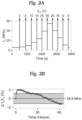
- FIG. 2 A is a graph of frequency vs. time showing steps of setting the frequency of a resonator, according to an embodiment of the invention.
- FIG. 2 B is a graph of ⁇ f V /f V vs. time after phototuning, showing stability of the resonator frequency, according to an embodiment of the invention.
- FIG. 2 C shows are graphs of results after 1800 erase/write cycles, showing reproducibility for many cycles of photodoping followed by erasure, according to an embodiment of the invention.
- FIG. 3 A are graphs showing photodoping curve plots of V mCNP (t) (upper) and f V (t) (lower), according to an embodiment of the invention.
- FIG. 3 B are graphs showing the doping rate vs. optical power for several gr/hBN and graphene devices, according to an embodiment of the invention.
- FIG. 3 C is a plot showing the tuning rate of a gr/hBN device at different wavelengths, according to an embodiment of the invention.
- FIG. 4 A is a graph showing the photodoping rate as the doping laser is swept across the drumhead, according to an embodiment of the invention.
- FIG. 4 B is a graph showing amplitude spectra for five different Gr/hBN devices, according to an embodiment of the invention.
- FIG. 4 C is a graph of resonance frequency gate curves for several different Gr/hBN devices, according to an embodiment of the invention.
- FIG. 5 is a schematic diagram of an optical setup that may be used to implement methods according to embodiments of the present invention.
- a reversible and long-lived frequency tuning of NEMS membrane resonators is provided.
- reversible and long-lived frequency tuning of graphene and graphene/hexagonal boron nitride (hBN) NEMS membrane resonators is provided.
- the technique uses spatially resolved photodoping of a membrane to generate locally-trapped, rewritable electrostatic charge which tensions the membrane and shifts its resonant frequency in a way equivalent to a local back gate.
- a bias is applied to a back-gate while focusing a laser onto the individual, suspended membrane of interest.
- the method is illustrated in the steps of FIG. 1 A .
- the NEMS device has a graphene/hBN membrane 100 suspended on a SiO 2 , layer 102 deposited on a Si substrate 104 that serves as a back gate. Contacts are provided to apply voltage bias between the graphene membrane and Si substrate. Writing and erasing the hBN/graphene NEMS memory is achieved as follows:
- Step 1 Initially, the laser and bias are both off, and the resonator will be at a frequency f 0 , which is typically on the order of 10 MHz.
- Step 2 With the laser off, apply a gate voltage V g between the graphene/hBN and the silicon back gate to tension the graphene/hBN membrane and increase (i.e., blue-shift) its frequency from f 0 to f V .
- V g is selected to achieve the desired frequency f V that will result from the subsequent photo-doping process (steps 2-3).
- Step 3 While continuing to apply V g , shine a laser on the graphene/hBN membrane to photoionize defects in hBN, doping the graphene, thereby removing the tension induced by the back-gate and detuning the resonance frequency away from f V toward f 0 . Given enough laser dose, the phototuning saturates, and the frequency approaches f 0 . Any visible light laser can be used to detune the membrane, but a blue laser (which has a higher energy per photon), and a higher power, has a faster detuning rate.
- Step 4 With the laser off, turn off the bias gate voltage V g .
- the graphene/hBN membrane will then shifts back to the frequency f V set in Step 2.
- the final phototuned frequency f V is determined by the initial value of V g , which we will call the doping potential, V d , and the illumination dose.
- Steps 1-4 complete the phototuning “write” function.
- the graphene/hBN membrane will remain at this frequency for several days with little or no change in frequency. This completes the memory writing operation.
- the drumhead state (i.e., its resonant frequency f V ) may be read by measuring the drumhead resonance frequency via optical interferometry.
- the memory of the written frequency state f V is long-lived, lasting several days to weeks with less than 1% change in f V (a high degree of non-volatility).
- the writing/erasing process reaches speeds exceeding 1 GHz/s, which can tune a typical resonator by a full line-width in ⁇ 100 ⁇ s, and has a tuning range of at least ⁇ 550%.
- the device can be rewritten a seemingly unlimited number of times with no observable degradation to the photo-tuning effect and with greater than 99% reproducibility.
- the spatial resolution of the tuning is diffraction limited, so it can address and write single micron-scale membranes and is scalable to large, chip-scale NEMS arrays which operates with only a single back-gate.
- the above steps can be used with slight modification to provide a method for photodetection. Incident radiation to be detected builds up charge which then strains the resonator. The total accumulated frequency shift of the resonator can be measured to determine the total accumulated light exposure through photo induced ionization.
- this method for photodetection of light with a nanoelectromechanical (NEMS) resonator has the following steps: applying a gate voltage between the drum membrane and a back gate, as in Step 2 above; turning on a light to expose the membrane to light to produce photoionization of the drum membrane such that a resulting charge alters the membrane resonant frequency, as in Step 3 above; turning off the light and releasing the gate voltage to set the resonant frequency of the membrane to a predetermined frequency, as in Step 4 above; exposing the drum membrane to the light to be detected to produce photoionization of the drum membrane such that a resulting charge alters the membrane resonant frequency, as in Step 5 above; and measuring the altered drumhead resonance frequency and comparing it to the predetermined frequency to determine total accumulated exposure of the drumhead to the light to be detected.
- NEMS nanoelectromechanical
- Example NEMS resonator devices and methods will now be illustrated in detail, together with results of experiments to characterize their properties.
- the phototuning effect was observed in NEMS membranes made from both graphene and a graphene/hBN heterostructure (gr/hBN).
- the triangles seen in FIG. 1 B are regions of multilayer hBN.
- the graphene and hBN were both synthesized by CVD.
- motion of the membranes is driven by applying an a.c. voltage to the back gate, and measure the motion with scanning optical interferometry and lock-in amplification.
- the interferometer is operated at a low power of ⁇ 10 ⁇ W and at 633 nm to minimize unwanted phototuning.
- mCNP mechanical charge neutrality point
- Phototuning causes V mCNP , and thus f V , to shift to a value determined by the doping potential, V d .
- Spectrograms for a gr/hBN device with and without photodoping are shown in FIGS. 1 D and 1 E , respectively.
- the doping potential V d was set to 0 (un-photodoped) and +30 V (photodoped), and the membrane was illuminated to saturation by rastering a relatively high power ( ⁇ 1 mW/ ⁇ m 2 ) 445 nm laser over the area of the drumhead.
- the un-photodoped V mCNP is several-hundred mV ( FIG. 1 D inset).
- V mCNP saturates close to V d , ⁇ 28 V in this case.
- the unbiased photodoped resonator behaves as if it were gated with an electrostatic potential of ⁇ V d .
- This potential can be described by the presence of charged defects in the h-BN or the oxide.
- V d shifts V mCNP
- the gate-dependence of each mode relative to V mCNP is independent of V d , as seen in FIGS. 1 D- 1 E . This demonstrates that the phototuning process does not alter the mechanical characteristics of the device in a measurable way.
- the zero-gate bias frequency f V also shifts.
- FIG. 2 A shows steps of setting the frequency in time.
- a combined high-power optical pulse of ⁇ 100 ⁇ J and gate voltage are applied at the times indicated by arrows.
- the steps in FIG. 2 A show that f V is stable for at least 600 s.
- f V is stable for at least 600 s.
- f V is detuned by 2% towards a higher frequency over the course of 2 hours; for a given device, the initial detuning is highly reproducible.
- the device slowly relaxes and f V red-shifts at a rate of 0.05%/hour.
- the mechanical linewidth for our devices is ⁇ 2% of the resonance frequency, so the frequency shifts by a linewidth in ⁇ 40 hours.
- the gray band shows the mechanical linewidth corresponding to a Q of 83.
- the phototuning method can achieve a high degree of frequency tuning repeatability, and can execute an indefinite number of write/erase cycles with no observable change to the phototuning effect or to the mechanical properties of the NEMS device.
- V d 0 V
- V d 30 V
- the writing process has a repeatability of 99.5%. The 0.5% repeatability uncertainty is partly due to the phototuning process, but also to other sources of frequency noise and fluctuations common to 2D NEMS, such as adsorbates, heating, and unwrinkling. After 1800 cycles, we did not observe any degradation to the phototuning efficiency or repeatability, or to the device's mechanical properties. We note that the large frequency separation of the written and erased states could easily allow a discrete binary logic state or, given the measured error of 190 kHz, over 150 discrete logic states.
- V mCNP and f V approach steady state values within ⁇ 10 ms.
- V mCNP saturates very close to V d .
- the saturation level varies by device, it is highly reproducible for a given device.
- V 0 mCNP is the initial V mCNP
- a is the doping rate, which depends on the laser's power, wavelength, and position.
- the V mCNP doping rate is
- df/dV g a
- df/dV g is the slope of the resonance frequency gate response at V 0 mCNP .
- ⁇ 5 V df/dV g is typically about 0.75 MHz/V, which with
- This frequency tuning rate of phototuning is exceptionally fast; for example, it could tune a resonator by a full linewidth is less than 1 ms. We note that this rate is the change in the steady-state f V for a particular dose, not the dynamic change in f V , which is limited by the RC time constant of the device.
- the frequency tuning rate is a vital aspect of any NEMS tuning approach. Among many things, the rate dictates the number of devices that can be tuned within a given time and sets limits on feedback control.
- FIG. 3 B shows the doping rate vs. optical power for several gr/hBN and graphene devices for powers ranging from 20-2000 ⁇ W.
- the photodoping rate depends on the value of V d relative to V 0 mCNP , with either V d ⁇ V 0 mCNP (a ⁇ branch) or V d >V 0 mCNP (a + branch).
- V d relative to V 0 mCNP
- V d >V 0 mCNP
- a + branch For all devices, a + >a ⁇ , but the difference can vary greatly; for most G/hBN devices, a + ⁇ 2a ⁇ , while for G devices a + ⁇ 10 3 ⁇ a ⁇ .
- the differences in the branch rates could be due to the activation dynamics or concentrations of the photoionized dopants; electron acceptors correspond to the a + branch since the ionized acceptor is negatively charged, but only if they are in the hBN.
- the dopants are in the glass, then the a + would be created by electron donors in the glass/Si interface, which leave behind positively charged ions.
- the similarity in the doping rates of the two branches in gr/hBN devices differs from other studies of the photoelectric memory effect, which found that a + ⁇ 200 ⁇ a ⁇ . This difference may be due to a different ratio of donors and acceptors in the CVD monolayer h-BN, compared to exfoliated thick h-BN. For instance, additional carbon defect acceptor states could be introduced in the CVD growth process. It is desirable to have comparable doping rates for the two branches because they allow rapid erasure and feedback g control of the device frequency.
- both a branches follow a power law relation, a ⁇ P ⁇ , where ⁇ is typically close to 1.5; the fits are shown as lines in the FIG. 3 B .
- the power law suggests that phototuning effect is not purely determined by dose, and is potentially due to local laser-induced heating of the Gr/hBN resonators, which lowers the energy barrier between the donors (acceptors) and the conduction (valence) bands.
- a for gr/hBN devices is greater than Gr devices, regardless of branch, although the difference is significantly larger for the a ⁇ branch, which can differ by a factor of 10 2 -10 3 .
- the phototuning rate is greater for shorter wavelength light.
- 8 V.
- FIG. 3 C shows the tuning rate, a, of a gr/hBN device, for both the positive and negative branches for 20 ⁇ W of 405 nm and 445 nm, 532 nm, and 633 nm illumination.
- the photodoping rate increases by a factor of 10 4 from 633 nm to 405 nm illumination.
- the rate increase also appears to be saturating near 3 eV.
- the enhanced phototuning at shorter wavelengths agrees with previous photodoping studies, and is consistent with the depths of a donor nitrogen vacancy (2.8 eV) and an acceptor carbon impurity (2.6 eV).
- the wavelength dependence of a is advantageous for nanomechanics experiments, as it allows selection of a long-wavelength laser for transduction, which has a negligible phototuning effect, and a short-wavelength laser for phototuning.
- FIG. 4 A shows the photodoping rate as the doping laser is swept across the drumhead. The doping rate is maximized at the center of the drum and rapidly falls off as it is swept away.
- FIG. 4 A also shows a cross-section of a for a 4.5 ⁇ m diameter membrane device (inset); the width of the gray-shaded region is equal to the diameter.
- Feedback could be used to correct this detuning drift or to further improve the overall f V tuning precision.
- the feedback control would be ultrafast because the frequency tuning rates can easily exceed ⁇ 1 GHz/s. At these high rates, a 1% error could be corrected in about 100 ⁇ s. Improved stability would likely be possible at cryogenic temperatures, which would reduce thermally-induced recombination of the ionized defects.
- Gr/h-BN mechanical drumhead resonators are fabricated by transferring the 2D sheets over an array of cavities etched into 1 ⁇ m wet thermal oxide grown on degenerately doped silicon wafers (University Wafer).
- the cavities are fabricated using direct-write optical lithography and CHF 3 based reactive ion etching. A ⁇ 300 nm layer of oxide is left at the bottom of the cavity to act as a charge trapping layer. Ti/Pt electrodes are then evaporated onto the chip.
- a relatively thick layer ( ⁇ 3 ⁇ m) of PMMA A11 is spun onto CVD grown single-layer h-BN on Cu foil (Graphene Supermarket) and then a polyamide scaffold with a central hole removed is then placed on the PMMA/hBN/Cu stack.
- the stack is placed in a bath of Ammonium Persulphate to etch the Cu and then rinsed in deionized water and dried in air.
- the polyamide/PMMA/hBN is placed on top of CVD graphene grown on Cu foil (Graphenea) and baked at 180 C for 30 minutes. The etching, rinsing, and drying is repeated leaving a freestanding film of PMMA/hBN/Graphene supported by the polyamide scaffold.
- the PMMA/hBN/Graphene stack was then placed on top of the pre-patterned cavities and adhered at 155 C overnight ( ⁇ 15 hours). After removing the polyamide scaffold, the PMMA was removed in flowing Ar/H 2 at 400 C. The graphene sheet contacts the electrodes from above, resulting in an electrical connection to all devices.
- Device motion was measured using optical interferometry.
- a 633 nm HeNe laser was focused onto the devices (held at room temperature at 10 ⁇ 6 Torr) using a 40 ⁇ , 0.6 NA objective.
- the reflected light is detected using a high-sensitivity photodiode (Thorlabs APD 130A).
- the voltage signal is measured using a Zurich Instruments HFLI2 Lock-In amplifier.
- the incident laser is scanned with a 2-axis galvometer and passed through an optical relay system in order to verify the mode shape and maximize transduction sensitivity.
- FSM Fast Steering Mirror
- PBS Polarizing Beamsplitter
- ⁇ /4 a Quarter Waveplate
- APD is an Avalanche Photodiode
- AOM is a Acousto-Optic Modulator
- DCM is a Dichroic Mirror.
- a separate laser (405 nm, 445 nm, or 532 nm) was used for photodoping.
- the doping laser was coupled into the beam-path using a dichroic mirror and focused onto the sample using the same 40 ⁇ , 0.6 NA objective lens.
- a separate 2-axis galvometer was used to position the doping laser in the center of the sample.
- the laser power for each color was calibrated using a power meter (Thorlabs 120VC) and maintained using PID control.
- An acousto-optic modulator was used to control the pulse length applied by the doping laser.
- Measurement of the mechanical charge neutrality point is typically accomplished by fitting the full frequency tuning curves (such as those shown in FIG. 1 D ), which is too slow for a dynamic measurement of V mCNP .
- the electrostatic force felt by the membrane is: F ⁇ (1 ⁇ 2)( dC g /dx )( V g ⁇ V mCNP ) 2 +V AC ( dC g /dx )( V g ⁇ V mCNP )cos(2 ⁇ ft+ ⁇ )
- the first term leads to frequency tuning and the second to electrostatic drive.
- our protocol is as follows. First, we set the drive frequency to 100 kHz and turn on the mechanical feedback. After a brief stabilization period, V g is measured 10 times with the average value giving V mCNP . V g is then fixed at and a short optical pulse is applied to the device to photodope it. This process is repeated until V mCNP approaches V d with both the laser power and pulse time determining the total length of the measurement.
- the invention provides devices and techniques for programmable NEMS crystals, which may be used as central processing units of analog and neuromorphic computers, or in acoustic materials.
- Platforms include a means to tune the frequencies of each individual cell of the crystal and the coupling between the cells.
- Our discovery provides a scalable means to achieve this tuning.
- one way to make these crystals is to pattern pillars on a silicon/silicon oxide substrate and transfer graphene to the pillars, like plastic wrap on a bed of nails.
- the fabrication of the pillars may be done with photo- and e-beam lithography and etching.
- These crystals can also be made by patterning coupled drumheads. For example, drumheads may be fabricated in an array with graphene ribbons connecting them.
- NEMS lattices Another application of these NEMS lattices is to metamaterials, which to be effective include a means to shift the frequency (or strain) of a resonator at high speeds. We have achieved this high speed shifting with the nanomechanical bolometer, which can shift at MHz rates. Combining fast frequency shifts with tunable crystals would let us make thermal or acoustic diodes. These diodes would let heat or sound go one way but not the other. These diodes are important to all-mechanical logic and thermal management. No natural material has these properties, but we can make a metamaterial that does. Thus, in combination with optically induced thermomechanical strain, it is feasible to construct dynamic, temporally modulated phononic crystals for novel metamaterial properties like non-reciprocal or topologically protected phonon transport.
- the inventors envision patterning arbitrary complex geometries of static charge across a single, large-area resonator. Such applications are similar to the programmable NEMS crystals, giving an alternative means to make the crystal. The crystal would have patterned strain, instead of patterned resonators.
- phototuned resonators may be used to build widely tunable bandpass filters.
- a resonator will absorb energy near the resonance frequency. So, the resonator will filter out signals near the resonance frequency, acting as a notch filter. The bandwidth of the notch filter is given by the linewidth of the resonator.
- the center frequency in our system is tunable. We have demonstrated a range of 7-45 MHz, but it is preferable to limit the frequency tuning voltage to 35 Volts just to be safe and not damage the devices. Embodiments may safely tune to 80-100 V and achieve a upper range near 100 MHz.
- This technique provides a method of specifying the mechanical resonance frequency in a re-writable fashion for multiplexed transduction.
- multiplexed readout is required and is typically achieved via changing the geometry of the NEMS.
- the resonant frequency is tuned after initial fabrication. First, the resonant frequency on all devices in an array is measured and the dose required to tune the resonance frequency using the aforementioned method is determined. Then, each device has its frequency tuned using the phototuning method until it is at the desired frequency. This frequency can be identical for all devices or spaced in a “comb” to allow discrimination of each devices.
- This technique provides a method for offsetting frequency drift to do irreversible processes such as mass adsorption.
- the frequency in NEMS oscillators is known to detune with time.
- the phototuning method can offset this detuning.
- the resonant frequency is set to a desired value.
- the frequency is periodically measured and the phototuning approach is used to restore the initial frequency.
- Phototuning offers intriguing possibilities for both applied and fundamental physics in NEMS and NEMS arrays, where tight control over individual resonators is essential.
- Our technique can pattern arbitrary complex geometries of static charge across a single, large-area resonator, which could improve the actuation efficiency of antisymmetric modes or allow tunable intermodal coupling, both commonly achieved via intricately patterned back-gates.
- Charge patterning could also enable electrostatic phononic crystals or new mechanisms for nanomechanical read-out by straining a suspended, photodoped p-n junction.
- phototuning provides a means to tune large arrays and lattices of 2D NEMS resonators, while only employing a single global back-gate and a single metallic top-contact.
- the spacing of individual resonators in these arrays is determined by the spatial resolution of phototuning ( ⁇ 1 ⁇ m in our setup), so highly dense arrays are possible. Due to the high tuning rates ( ⁇ GHz/s), phototuning can rapidly program and control these dense arrays.
- Precisely tuned resonator arrays will have many new applications, including spatially resolved imaging or multiplexed sensing for force, charge, or mass spectrometry.
- An array can serve as a new type of photodetector array similar to a CCD, where a projected optical image could be recorded by measuring the cumulative frequency shift of each array element.
- the persistence and large tuning range of phototuning combined with an array would permit high-density memory storage, where information is encoded in the frequency of each resonator. If each memory state is separated by a resonance linewidth ( ⁇ 100 kHz), the tuning range demonstrated in FIG. 2 A would accommodate ⁇ 543 states, which is equivalent to a 9-bit memory with a lifetime of ⁇ 40 hours.
- the areal bit density of an array would exceed a Gbit/in 2 .
- the density could be greatly improved by reducing the frequency binning to a level closer to the frequency noise, which is typically ⁇ 100 Hz at room temperature. For example, a bin of 1 kHz would yield a bit density of ⁇ 100 Gbit/in 2 , a value exceeding modern optical media by 10 ⁇ .
- This tuning also offers new opportunities for programmable NEMS crystals. In our vision for these crystals, individual Gr/hBN or Gr resonators would be coupled to neighboring resonators by a suspended bridge of Gr/hBN or Gr. By phototuning the resonators and the bridges, precisely tuned complex acoustic crystals would possible.
- the trapped charge applies an electrostatic force on the graphene, which shifts its frequency and the V mCNP .
- the frequency shift is determined by the doping potential and the dose.
- the total charge begins to neutralize under an applied bias, and the force vanishes completely when V g ⁇ V mCNP .
- the locally trapped charge can reside in the hBN and the oxide/silicon interface.
- photodoping rates are much faster in the gr/hBN heterostructure.
- Phototuning could be used in a variety of systems which undergo photoinduced doping, such as SrTiO 3 , graphene/dielectric layers, or other graphene based 2D heterostructures.
- the mechanical element does not need to be graphene or an atomically-thin graphene hybrid.
- graphene-coated silicon nitride nanobeams could be persistently tuned but would retain ultra-high quality factors of Q>10 6 , allowing for an extremely dense analog memory.
- the advantage of atomically-thin resonators will be an extreme tuning range.
- phototuning is useful for patterning local strain.
- phototuning enables sophisticated electrostatic force landscapes in NEMS that are otherwise impossible to realize.
- Coupled NEMS resonators for example, are challenging to study because they require close spacing and tunable frequencies and coupling, both of which are easily accomplished with phototuning.
- phototuning opens the door to advanced NEMS resonator networks.
- Phototuned resonators can be used to build many valuable network components like widely tunable bandpass filters, high-density analog memories, and acoustic waveguides.
- our platform makes both the node coupling and the nodes of the network programmable, which would enable programmable phononic crystals for tunable phononic cavities, tunable thermal transport, or a potential framework for mechanical analog logic and computing.
- programmable phononic crystals for tunable phononic cavities, tunable thermal transport, or a potential framework for mechanical analog logic and computing.
- optically induced thermomechanical strain it would be feasible to construct dynamic, temporally modulated phononic crystals for novel metamaterial properties like non-reciprocal or topologically protected phonon transport.
Abstract
Description
-
- applying a gate voltage between the drum membrane and a back gate to alter the resonant frequency of the membrane to a desired frequency;
- photoionizing the drum membrane with a laser to detune the membrane resonant frequency to a ground state frequency;
- releasing the gate voltage to set the membrane to the desired resonant frequency.
-
- applying a gate voltage between the drum membrane and a back gate,
- exposing the membrane to light to produce photoionization of the drum membrane such that a resulting charge alters the membrane resonant frequency,
- turning off the light and releasing the gate voltage to set the resonant frequency of the membrane to a predetermined frequency;
- exposing the drum membrane to the light to produce photoionization of the drum membrane such that a resulting charge alters the membrane resonant frequency;
- measuring the drumhead resonance frequency and comparing it to the predetermined frequency to determine total accumulated exposure of the drumhead to the light.
V mCNP(t)=ΔV(1−e −at)+V 0 mCNP
|dV mCNP(t)/dt|=|ΔV|a,
and the frequency tuning rate is
R f =|dV mCNP(t)/dt|df/dV g =a|ΔV|df/dV g,
F≈(½)(dC g /dx)(V g −V mCNP)2 +V AC(dC g /dx)(V g −V mCNP)cos(2πft+θ)
Claims (10)
Priority Applications (1)
| Application Number | Priority Date | Filing Date | Title |
|---|---|---|---|
| US17/613,192 US11862265B2 (en) | 2019-05-27 | 2020-05-27 | Mechanical memory and tunable nano-electromechanical systems (NEMS) resonator |
Applications Claiming Priority (3)
| Application Number | Priority Date | Filing Date | Title |
|---|---|---|---|
| US201962853161P | 2019-05-27 | 2019-05-27 | |
| US17/613,192 US11862265B2 (en) | 2019-05-27 | 2020-05-27 | Mechanical memory and tunable nano-electromechanical systems (NEMS) resonator |
| PCT/US2020/034750 WO2020243201A1 (en) | 2019-05-27 | 2020-05-27 | Mechanical memory and tunable nano-eletromechanical system (nems) resonator |
Publications (2)
| Publication Number | Publication Date |
|---|---|
| US20220238172A1 US20220238172A1 (en) | 2022-07-28 |
| US11862265B2 true US11862265B2 (en) | 2024-01-02 |
Family
ID=73552663
Family Applications (1)
| Application Number | Title | Priority Date | Filing Date |
|---|---|---|---|
| US17/613,192 Active 2040-12-27 US11862265B2 (en) | 2019-05-27 | 2020-05-27 | Mechanical memory and tunable nano-electromechanical systems (NEMS) resonator |
Country Status (2)
| Country | Link |
|---|---|
| US (1) | US11862265B2 (en) |
| WO (1) | WO2020243201A1 (en) |
Families Citing this family (2)
| Publication number | Priority date | Publication date | Assignee | Title |
|---|---|---|---|---|
| CN113517392A (en) * | 2021-03-08 | 2021-10-19 | 复旦大学 | Gating device based on two-dimensional material and used for 3D integration and preparation method thereof |
| CN114659625B (en) * | 2022-03-17 | 2023-04-25 | 电子科技大学 | Performance-adjustable bolometer based on graphene mechanical vibrator and preparation method |
Citations (5)
| Publication number | Priority date | Publication date | Assignee | Title |
|---|---|---|---|---|
| US6922272B1 (en) * | 2003-02-14 | 2005-07-26 | Silicon Light Machines Corporation | Method and apparatus for leveling thermal stress variations in multi-layer MEMS devices |
| US20050242904A1 (en) | 2004-04-28 | 2005-11-03 | Markus Lutz | Method for adjusting the frequency of a MEMS resonator |
| US20130135620A1 (en) * | 2011-11-30 | 2013-05-30 | Qualcomm Mems Technologies, Inc. | Systems and methods for non-invasive testing of electromechanical systems devices |
| US20150300999A1 (en) | 2012-10-02 | 2015-10-22 | Commissariat A L'energie Atomique Et Aux Energies Alternatives | Measurement system including a network of nanoelectromechanical system resonators |
| US20200174192A1 (en) * | 2018-12-04 | 2020-06-04 | Imec Vzw | Method for manufacturing a waveguide for guiding an electro-magnetic wave |
-
2020
- 2020-05-27 WO PCT/US2020/034750 patent/WO2020243201A1/en active Application Filing
- 2020-05-27 US US17/613,192 patent/US11862265B2/en active Active
Patent Citations (5)
| Publication number | Priority date | Publication date | Assignee | Title |
|---|---|---|---|---|
| US6922272B1 (en) * | 2003-02-14 | 2005-07-26 | Silicon Light Machines Corporation | Method and apparatus for leveling thermal stress variations in multi-layer MEMS devices |
| US20050242904A1 (en) | 2004-04-28 | 2005-11-03 | Markus Lutz | Method for adjusting the frequency of a MEMS resonator |
| US20130135620A1 (en) * | 2011-11-30 | 2013-05-30 | Qualcomm Mems Technologies, Inc. | Systems and methods for non-invasive testing of electromechanical systems devices |
| US20150300999A1 (en) | 2012-10-02 | 2015-10-22 | Commissariat A L'energie Atomique Et Aux Energies Alternatives | Measurement system including a network of nanoelectromechanical system resonators |
| US20200174192A1 (en) * | 2018-12-04 | 2020-06-04 | Imec Vzw | Method for manufacturing a waveguide for guiding an electro-magnetic wave |
Non-Patent Citations (5)
| Title |
|---|
| Cai et al. Efficient Photoinduced Charge Accumulation in Reduced Graphene Oxide Coupled with Titania Nanosheets to Show Highly Enhanced and Persistent Conductance. Appl. Mater. Interf. 2015, 11436-43. |
| Choi et al. Photoelectric Memory Effect in Graphene Heterostructure Field-Effect Transistors Based on Dual Dielectrics. ACS Photonics 2018, 5: 329-336. |
| IEEE MEMS 2022, Tokyo, JAPAN Jan. 9-13, 2022; Nanoelectromechanical Memories Basedonnonlinear 2D MoS2 Resonators Pengcheng Zhang et al.(Year: 2022). * |
| Kim et al. Focused-Laser Enabled p—n Junctions in Graphene Field-Effect Transistors. ACS Nano 7(7) 2013 5850-5857. |
| Miller et al. Non-volatile rewritable frequency turning of a nonelectromechanical resonator using photoinduced doping. Nano Letters 20(4) 2020 2378-2380. |
Also Published As
| Publication number | Publication date |
|---|---|
| WO2020243201A1 (en) | 2020-12-03 |
| US20220238172A1 (en) | 2022-07-28 |
Similar Documents
| Publication | Publication Date | Title |
|---|---|---|
| US11862265B2 (en) | Mechanical memory and tunable nano-electromechanical systems (NEMS) resonator | |
| Smith et al. | Picosecond photoconductivity in radiation‐damaged silicon‐on‐sapphire films | |
| Jelken et al. | Light induced reversible structuring of photosensitive polymer films | |
| US20210203352A1 (en) | Method of coding based on transition of lasing and non-lasing states of optical structure | |
| Wesner et al. | Temporal development of photorefractive solitons up to telecommunication wavelengths in strontium-barium niobate waveguides | |
| JPH0242424A (en) | Optical correlator | |
| Ascienzo | Nonlinear Optical Studies of Defects and Domain Structures in Perovskite-Type Dielectric Ceramics | |
| Ding et al. | Comparative study of photo-induced electronic transport along ferroelectric domain walls in lithium niobate single crystals | |
| Shiau et al. | Real-time phase difference control of optical beams using a Mach–Zehnder interferometer | |
| Kabir | Synthesis of Ca x Ba 1₋ x Nb₂O₅ Thin Films on Lattice Matched Gd₃Ga₅O₁₂ Substrate by Pulsed Laser Deposition | |
| Miller | Shaping, Tuning, and Playing Nanodrums: Towards Scalable and High Quality Factor Graphene Nanoelectromechanical Systems | |
| RU2772926C1 (en) | Method for manufacturing an element based on ferroelectric hafnium oxide for switchable opto- and microelectronics devices | |
| Schröder | Conductive domain walls in ferroelectric bulk single crystals | |
| Bundulis et al. | Z-scan extensions for inclusive study of nonlinear refractive index | |
| Kurt | Nonlinear Optical Studies of Structural Defects in Perovskite Dielectric and Ferroelectric Oxides for Energy Storage Applications | |
| Yang | Photoelectric processes in ferroelectric/multiferroic materials | |
| Ebothé et al. | Photoinduced second-harmonic generation in the indium tin oxide crystalline films | |
| Chao et al. | FOURIER-TRANSFORM INFRARED SPECTROSCOPIC STUDY OF OXIDE-FILMS GROWN IN PURE N2O | |
| Wada et al. | Characterization of femtosecond laser pulses with GaN thin films | |
| Vargas | A CMOS compatible ferroelectric tunnel junction memory device | |
| Foster | Engineering and control of advanced optoelectronic materials for applications in quantum devices | |
| Montenegro et al. | Photorefractive two-wave mixing phase coupling measurement in a self-stabilized recording regime | |
| Horn et al. | Ultrafast pump & probe investigations on the interaction of femtosecond laser pulses with glass | |
| Li | Engineering and Nanophotonics with Single Photon Emitters in Hexagonal Boron Nitride | |
| Chen | ULTRAFAST OPTICAL RESPONSE AND TRANSPORT PROPERTIES OF STRONTIUM TITANATE-BASED COMPLEX OXIDE NANOSTRUCTURES |
Legal Events
| Date | Code | Title | Description |
|---|---|---|---|
| AS | Assignment |
Owner name: UNIVERSITY OF OREGON, OREGON Free format text: ASSIGNMENT OF ASSIGNORS INTEREST;ASSIGNORS:ALEMAN, BENJAMIN J.;MILLER, DAVID J.;REEL/FRAME:058178/0911 Effective date: 20200513 |
|
| FEPP | Fee payment procedure |
Free format text: ENTITY STATUS SET TO UNDISCOUNTED (ORIGINAL EVENT CODE: BIG.); ENTITY STATUS OF PATENT OWNER: SMALL ENTITY |
|
| FEPP | Fee payment procedure |
Free format text: ENTITY STATUS SET TO SMALL (ORIGINAL EVENT CODE: SMAL); ENTITY STATUS OF PATENT OWNER: SMALL ENTITY |
|
| STPP | Information on status: patent application and granting procedure in general |
Free format text: DOCKETED NEW CASE - READY FOR EXAMINATION |
|
| STPP | Information on status: patent application and granting procedure in general |
Free format text: NOTICE OF ALLOWANCE MAILED -- APPLICATION RECEIVED IN OFFICE OF PUBLICATIONS |
|
| STPP | Information on status: patent application and granting procedure in general |
Free format text: PUBLICATIONS -- ISSUE FEE PAYMENT RECEIVED |
|
| STPP | Information on status: patent application and granting procedure in general |
Free format text: PUBLICATIONS -- ISSUE FEE PAYMENT VERIFIED |
|
| STCF | Information on status: patent grant |
Free format text: PATENTED CASE |
|
| CC | Certificate of correction |