US11747223B2 - Strain inducing body and force sensor device with improved load bearing - Google Patents

Strain inducing body and force sensor device with improved load bearing Download PDF

Info

Publication number
US11747223B2
US11747223B2 US17/645,086 US202117645086A US11747223B2 US 11747223 B2 US11747223 B2 US 11747223B2 US 202117645086 A US202117645086 A US 202117645086A US 11747223 B2 US11747223 B2 US 11747223B2
Authority
US
United States
Prior art keywords
strain inducing
force
moment
detection beam
sensor chip
Prior art date
Legal status (The legal status is an assumption and is not a legal conclusion. Google has not performed a legal analysis and makes no representation as to the accuracy of the status listed.)
Active
Application number
US17/645,086
Other versions
US20220205854A1 (en
Inventor
Shinya Yamaguchi
Current Assignee (The listed assignees may be inaccurate. Google has not performed a legal analysis and makes no representation or warranty as to the accuracy of the list.)
MinebeaMitsumi Inc
Original Assignee
MinebeaMitsumi Inc
Priority date (The priority date is an assumption and is not a legal conclusion. Google has not performed a legal analysis and makes no representation as to the accuracy of the date listed.)
Filing date
Publication date
Application filed by MinebeaMitsumi Inc filed Critical MinebeaMitsumi Inc
Assigned to MINEBEA MITSUMI INC. reassignment MINEBEA MITSUMI INC. ASSIGNMENT OF ASSIGNORS INTEREST (SEE DOCUMENT FOR DETAILS). Assignors: YAMAGUCHI, SHINYA
Publication of US20220205854A1 publication Critical patent/US20220205854A1/en
Application granted granted Critical
Publication of US11747223B2 publication Critical patent/US11747223B2/en
Active legal-status Critical Current
Anticipated expiration legal-status Critical

Links

Images

Classifications

    • GPHYSICS
    • G01MEASURING; TESTING
    • G01LMEASURING FORCE, STRESS, TORQUE, WORK, MECHANICAL POWER, MECHANICAL EFFICIENCY, OR FLUID PRESSURE
    • G01L5/00Apparatus for, or methods of, measuring force, work, mechanical power, or torque, specially adapted for specific purposes
    • G01L5/16Apparatus for, or methods of, measuring force, work, mechanical power, or torque, specially adapted for specific purposes for measuring several components of force
    • G01L5/161Apparatus for, or methods of, measuring force, work, mechanical power, or torque, specially adapted for specific purposes for measuring several components of force using variations in ohmic resistance
    • G01L5/162Apparatus for, or methods of, measuring force, work, mechanical power, or torque, specially adapted for specific purposes for measuring several components of force using variations in ohmic resistance of piezoresistors
    • GPHYSICS
    • G01MEASURING; TESTING
    • G01LMEASURING FORCE, STRESS, TORQUE, WORK, MECHANICAL POWER, MECHANICAL EFFICIENCY, OR FLUID PRESSURE
    • G01L1/00Measuring force or stress, in general
    • G01L1/18Measuring force or stress, in general using properties of piezo-resistive materials, i.e. materials of which the ohmic resistance varies according to changes in magnitude or direction of force applied to the material
    • GPHYSICS
    • G01MEASURING; TESTING
    • G01LMEASURING FORCE, STRESS, TORQUE, WORK, MECHANICAL POWER, MECHANICAL EFFICIENCY, OR FLUID PRESSURE
    • G01L1/00Measuring force or stress, in general
    • G01L1/20Measuring force or stress, in general by measuring variations in ohmic resistance of solid materials or of electrically-conductive fluids; by making use of electrokinetic cells, i.e. liquid-containing cells wherein an electrical potential is produced or varied upon the application of stress
    • G01L1/22Measuring force or stress, in general by measuring variations in ohmic resistance of solid materials or of electrically-conductive fluids; by making use of electrokinetic cells, i.e. liquid-containing cells wherein an electrical potential is produced or varied upon the application of stress using resistance strain gauges
    • G01L1/2206Special supports with preselected places to mount the resistance strain gauges; Mounting of supports
    • GPHYSICS
    • G01MEASURING; TESTING
    • G01LMEASURING FORCE, STRESS, TORQUE, WORK, MECHANICAL POWER, MECHANICAL EFFICIENCY, OR FLUID PRESSURE
    • G01L1/00Measuring force or stress, in general
    • G01L1/26Auxiliary measures taken, or devices used, in connection with the measurement of force, e.g. for preventing influence of transverse components of force, for preventing overload

Definitions

  • the present disclosure relates to a strain inducing body and a force sensor device.
  • a force sensor device includes a structure including (i) a sensor chip, (ii) an external force receiving plate that is disposed around the sensor chip and to which an external force is applied, (iii) a base that supports the sensor chip, (iv) an external force-buffering mechanism that secures the external force receiving plate to the base, and (v) a coupling rod that is an external force-transmitting mechanism, where the external force receiving plate and an effect portion are coupled to each other by the coupling rod (see, e.g., Patent Document 1).
  • an object of the present disclosure is to provide a sensor chip with increased fracture resistance, while transmitting a displacement appropriately.
  • a strain inducing body includes a strain inducing portion.
  • the strain inducing portion includes a movable portion configured to receive a force in a predetermined axial direction or a moment about the predetermined axial direction and to deform in accordance with the received force or moment.
  • the strain inducing portion includes a non-movable portion configured to receive the force or moment and to not deform in accordance with the received force or moment.
  • the strain inducing body includes an input transmitter coupled to the non-movable portion and including an accommodating portion for accommodating a sensor chip configured to detect the force or moment.
  • the input transmitter is configured to receive the force or moment and to not deform in accordance with the received force or moment and to transmit deformation of the strain inducing portion to the sensor chip.
  • a strain inducing body with increased fracture resistance, while transmitting a displacement appropriately can be provided.
  • FIG. 1 is a perspective view of a force sensor device according to a first embodiment
  • FIG. 2 is a cross-sectional perspective view of the force sensor device according to the first embodiment
  • FIG. 3 is a perspective top view of a sensor chip attached to an input transmitter
  • FIG. 4 is a perspective bottom view of the sensor chip attached to the input transmitter
  • FIG. 5 is a perspective view of a sensor chip 100 when viewed in a positive Z-axis direction;
  • FIG. 6 is a plan view of the sensor chip 100 when viewed in the positive Z-axis direction;
  • FIG. 7 is a perspective view of the sensor chip 100 when viewed in a negative Z-axis direction
  • FIG. 8 is a bottom view of the sensor chip 100 when viewed in the negative Z-axis direction;
  • FIG. 9 is a diagram for describing signs for forces and moments applied to axes.
  • FIG. 10 is a diagram illustrating an example of the arrangement of piezoresistive elements of the sensor chip 100 ;
  • FIG. 11 is a partial enlarged view of the sensor chip in one sensing block illustrated in FIG. 10 ;
  • FIG. 12 is a diagram (first part) illustrating an example of a detecting circuit that uses piezoresistive elements
  • FIG. 13 is a diagram (second part) illustrating an example of the detecting circuit that uses piezoresistive elements
  • FIG. 14 is a diagram for describing an input Fx
  • FIG. 15 is a diagram for describing an input Fy
  • FIG. 16 is a diagram illustrating a simulation result when the input Fx is applied to the sensor chip
  • FIG. 17 is a diagram illustrating a simulation result when an input Mz is applied to the sensor chip
  • FIG. 18 is a diagram illustrating a simulation result when an input Fz is applied to the sensor chip
  • FIG. 19 is a partial perspective view of the sensor chip illustrated in FIG. 18 ;
  • FIG. 20 is a perspective view of a force receiving plate included in a strain inducing body
  • FIG. 21 is a perspective view of a strain inducing portion included in the strain inducing body
  • FIG. 22 is a perspective top view of an input transmitter included in the strain inducing body
  • FIG. 23 is a perspective bottom view of the input transmitter included in the strain inducing body
  • FIG. 24 is a side view of the input transmitter included in the strain inducing body
  • FIG. 25 is a perspective view of a cover plate included in the strain inducing body
  • FIG. 26 is a diagram illustrating the simulation result when the input Fx is applied to the strain inducing portion
  • FIG. 27 is a diagram illustrating the simulation result when the input Mz is applied to the strain induction section
  • FIG. 28 is a plan view of a sensor chip 100 A when viewed in the positive Z-axis direction;
  • FIG. 29 is a partial plan view of a sensor chip 100 B when viewed in the positive Z-axis direction;
  • FIG. 30 is a partial plan view of a sensor chip 100 C when viewed in the positive Z-axis direction;
  • FIG. 31 is a perspective view of a strain inducing body 200 A
  • FIG. 32 is a cross-sectional perspective view of the strain inducing body 200 A
  • FIG. 33 is a perspective view of the input transmitter included in the strain inducing body
  • FIG. 34 is a perspective view of the cover plate included in the strain inducing body
  • FIG. 35 is a side view of a strain inducing body 200 B.
  • FIG. 36 is a perspective bottom view of the strain inducing portion included in the strain inducing body.
  • FIG. 1 is a perspective view of a force sensor device according to a first embodiment.
  • FIG. 2 is a cross-sectional perspective view of the force sensor device according to the first embodiment.
  • the force sensor device 1 includes a sensor chip 100 and a strain inducing body 200 .
  • the force sensor device 1 is, for example, a multi-axis force sensor device provided in an arm, a finger, or the like of a robot that is used for a machine tool or the like.
  • the sensor chip 100 has a function of detecting up to six axes relating to displacements in predetermined axial directions.
  • the strain inducing body 200 has a function of transmitting at least one among an applied force and a moment, to the sensor chip 100 .
  • a case in which the sensor chip 100 detects six axes will be described, but there is no limitation to such a sensor chip.
  • the sensor chip 100 that detects three axes or the like can be adopted.
  • the strain inducing body 200 includes a force receiving plate 210 , a strain inducing portion 220 , an input transmitter 230 , and a cover plate 240 .
  • the strain inducing portion 220 is layered on the force receiving plate 210
  • the input transmitter 230 is layered on the strain inducing portion 220
  • the cover plate 240 is layered on the input transmitter 230 .
  • the strain inducing body 200 is substantially cylindrical as a whole.
  • the function of the strain inducing body 200 is mainly implemented by the strain inducing portion 220 and the input transmitter 230 , and thus the force receiving plate 210 and the cover plate 240 may be provided as needed.
  • the side of the cover plate 240 is referred to as a top side or one side, and the side of the force receiving plate 210 is referred to as a bottom side or another side. Further, for each component, the surface on the side of the cover plate 240 is referred to as one surface or a top surface, and the surface on the side of the force receiving plate 210 is referred to as another surface or a bottom surface.
  • the force sensor device 1 may be used in a state of being upside down, or can be disposed at any angle.
  • a plan view means that an object is viewed in a direction (Z-axis direction) normal to the top surface of the cover plate 240
  • a planar shape refers to a shape of the object when viewed in the direction (Z-axial direction) normal to the top surface of the cover plate 240 .
  • FIG. 3 is a perspective top view of the sensor chip attached to the input transmitter.
  • FIG. 4 is a perspective bottom view of the sensor chip attached to the input transmitter.
  • an accommodating portion that protrudes from the bottom surface of the input transmitter 230 , toward the strain inducing portion 220 , is provided in the input transmitter 230 .
  • the sensor chip 100 is secured to the accommodating portion 235 toward the cover plate 240 .
  • second connection portions 235 c (see FIGS. 22 to 24 and the like below) each of which enters the cover plate 240 are disposed in the accommodating portion 235 .
  • the second connection portions 235 c are respectively connected to the bottom surfaces of force point portions 151 to 154 (see FIGS. 5 to 8 and the like below) of the sensor chip 100 .
  • the accommodating portion 235 enters the strain inducing portion 220 .
  • first connection portions 224 (see FIG. 21 below), which are five columnar portions and protrude toward the input transmitter 230 , are disposed in the strain inducing portion 220 .
  • the first connection portions 224 are respectively connected to bottom surfaces of the supports 101 to 105 (see FIGS. 5 to 8 and the like below) in the sensor chip 100 .
  • the word “parallel” is intended to include a case in which an angle between two straight lines or sides is in the range of 0° ⁇ 10°.
  • the word “vertical” or “perpendicular” is intended to include a case in which an angle between two straight lines or between sides is in the range of 90° ⁇ 10°.
  • the word “center” and “middle” are intended to include an approximate center and middle of an object, and are not intended to mean only an exact center and middle. In other words, variations in manufacturing error shall be tolerable. The same applies to point symmetry and line symmetry.
  • FIG. 5 is a perspective view of the sensor chip 100 when viewed in the positive Z-axis direction.
  • FIG. 6 is a plan view of the sensor chip 100 when viewed in the positive Z-axis direction.
  • FIG. 7 is a perspective view of the sensor chip 100 when viewed in the negative Z-axis direction.
  • FIG. 8 is a bottom view of the sensor chip 100 when viewed in the negative Z-axis direction. In FIG. 8 , for the sake of convenience, surfaces at the same height are illustrated in the same crepe pattern.
  • a direction parallel to one side of the top surface of the sensor chip 100 refers to the X-axis direction
  • a direction perpendicular to the one side of the top surface of the sensor chip 100 refers to the Y-axis direction
  • a thickness direction (direction normal to the top surface of the sensor chip 100 ) of the sensor chip 100 refers to the Z-axis direction.
  • the X-axis direction, the Y-axis direction, and the Z-axis direction are mutually perpendicular.
  • the sensor chip 100 illustrated in FIGS. 5 to 8 is a microelectromechanical systems (MEMS) sensor chip that is one chip and can detect up to six axes.
  • the sensor chip 100 is formed of a semiconductor substrate such as a silicon on insulator (SOI) substrate.
  • SOI silicon on insulator
  • the planar shape of the sensor chip 100 can be, for example, an approximate 7000 ⁇ m per side rectangle (square or rectangle).
  • the sensor chip 100 includes five columnar supports 101 to 105 .
  • the planar shape of each of the supports 101 to 105 can be, for example, an approximate 2000 ⁇ m per side square.
  • the supports 101 to 104 are respectively disposed at four corners of the rectangular sensor chip 100 .
  • the support 105 is disposed on a central portion of the rectangular sensor chip 100 .
  • Each of the supports 101 to 104 is a representative example of a first support, and the support 105 is a representative example of a second support.
  • a frame 112 (for coupling supports that are next to each other), of which both ends are fixed by the support 101 and the support 102 , is provided between the support 101 and the support 102 .
  • a frame 113 (for coupling supports that are next to each other), of which both ends are fixed by the support 102 and the support 103 , is provided between the support 102 and the support 103 .
  • a frame 114 (for coupling supports that are next to each other), of which both ends are fixed by the support 103 and the support 104 , is provided between the support 103 and the support 104 .
  • a frame 111 (for coupling supports that are next to each other), of which both ends are fixed by the support 104 and the support 101 , is provided between the support 104 and the support 101 .
  • four frames 111 , 112 , 113 , and 114 are formed as a structural frame of the sensor chip 100 , and the supports 101 , 102 , 103 , and 104 are each disposed at a corner at which given frames are coupled to each other.
  • An internal corner of the support 101 and a corner of the support 105 facing the internal corner of the support 101 are coupled by a coupling portion 121 .
  • An internal corner of the support 102 and a corner of the support 105 facing the internal corner of the support 102 are coupled by a coupling portion 122 .
  • An internal corner of the support 103 and a corner of the support 105 facing the internal corner of the support 103 are coupled by a coupling portion 123 .
  • An internal corner of the support 104 and a corner of the support 105 facing the internal corner of the support 104 are coupled by a coupling portion 124 .
  • the sensor chip 100 includes the coupling portions 121 to 124 each of which couples the support 105 and a given support among the supports 101 to 104 .
  • the coupling portions 121 to 124 are each disposed diagonally relative to the X-axis direction (Y-axis direction).
  • the coupling portions 121 to 124 are respectively disposed so as not to be parallel to the frames 111 , 112 , 113 , and 114 .
  • the supports 101 to 105 , the frames 111 to 114 , and the coupling portions 121 to 124 can be each formed of, for example, an active layer, a BOX layer, and a support layer of the SOI substrate.
  • the thickness of each of those layers can be, for example, in the range of about 400 ⁇ m to about 600 ⁇ m.
  • the sensor chip 100 has four sensing blocks B 1 to B 4 .
  • Each sensing block includes three T-patterned beam structures in each of which piezoresistive elements being strain-detecting elements are disposed.
  • the T-patterned beam structure refers to a structure that includes a first detection beam and a second detection beam that extends from a middle portion of the first detection beam in a direction perpendicular to the first detection beam.
  • the sensing block B 1 includes T-patterned beam structures 131 T 1 , 131 T 2 , and 131 T 3 .
  • the sensing block B 2 includes T-patterned beam structures 132 T 1 , 132 T 2 , and 132 T 3 .
  • the sensing block B 3 includes T-patterned beam structures 133 T 1 , 133 T 2 , and 133 T 3 .
  • the sensing block B 4 includes T-patterned beam structures 134 T 1 , 134 T 2 , and 134 T 3 .
  • the beam structure will be described below in more details.
  • a first detection beam 131 a is provided parallel to a side of the support 104 toward the support 101 so as to be at a predetermined distance from the side of the support 104 .
  • the first detection beam 131 a extends between the frame 111 , toward the support 101 , and the coupling portion 121 , toward the support 105 .
  • a second detection beam 131 b is provided such that one end of the second detection beam is coupled at a middle portion of the first detection beam 131 a in a longitudinal direction of the first detection beam.
  • the second detection beam 131 b extends toward the support 104 in a direction perpendicular to the longitudinal direction of the first detection beam 131 a .
  • the first detection beam 131 a and the second detection beam 131 b constitute the T-patterned beam structure 131 T 1 .
  • a first detection beam 131 c is provided parallel to a side of the support 104 toward the support 101 so as to be at a predetermined distance from the side of the support 104 .
  • the first detection beam 131 c extends between the coupling portion 111 , toward the support 104 , and the coupling portion 124 , toward the support 105 .
  • a second detection beam 131 d is provided such that one end of the second detection beam is coupled at a middle portion of the first detection beam 131 c in a longitudinal direction of the first detection beam.
  • the second detection beam 131 d extends toward the support 101 in a direction perpendicular to the longitudinal direction of the first detection beam 131 c .
  • the first detection beam 131 c and the second detection beam 131 d constitute the T-patterned beam structure 131 T 2 .
  • a first detection beam 131 e is provided parallel to a side of the support 105 toward the frame 111 so as to be at a predetermined distance from the side of the support 105 .
  • the first detection beam 131 e extends between the coupling portion 121 , toward the support 105 , and the coupling portion 124 , toward the support 105 .
  • a second detection beam 131 f is provided such that one end of the second detection beam is coupled at a middle portion of the first detection beam 131 e in a longitudinal direction, and the second detection beam 131 f extends toward the frame 111 in a direction perpendicular to the longitudinal direction of the first detection beam 131 e .
  • the first detection beam 131 e and the second detection beam 131 f constitute the T-patterned beam structure 131 T 3 .
  • connection portion 141 Another end of the second detection beam 131 b , another end of the second detection beam 131 d , and another end of the second detection beam 131 f are connected to one another to thereby form a connection portion 141 .
  • a force point portion 151 is provided at the bottom surface of the connection portion 141 .
  • the force point portion 151 has, for example, a rectangular prismatic shape.
  • the T-patterned beam structures 131 T 1 , 131 T 2 , and 131 T 3 , the connection portion 141 , and the force point portion 151 constitute the sensing block B 1 .
  • the first detection beam 131 a , the first detection beam 131 c , and the second detection beam 131 f are parallel to one another.
  • the second detection beams 131 b and 131 d , and the first detection beam 131 e are parallel to one another.
  • the thickness of each detection beam in the sensing block B 1 can be, for example, in the range of about 30 ⁇ m to about 50 ⁇ m.
  • a first detection beam 132 a is provided parallel to a side of the support 102 toward the support 101 so as to be at a predetermined distance from the side of the support 102 .
  • the first detection beam 132 a extends between the frame 112 , toward the support 102 , and the coupling portion 122 , toward the support 105 .
  • a second detection beam 132 b is provided such that one end of the second detection beam is coupled at a middle portion of the first detection beam 132 a in a longitudinal direction of the first detection beam.
  • the second detection beam 132 b extends toward the support 101 in a direction perpendicular to the longitudinal direction of the first detection beam 132 a .
  • the first detection beam 132 a and the second detection beam 132 b constitute the T-patterned beam structure 131 T 2 .
  • a first detection beam 132 c is provided parallel to a side of the support 101 toward the support 102 so as to be at a predetermined distance from the side of the support 101 .
  • the first detection beam 132 c extends between the frame 112 , toward the support 101 , and the coupling portion 121 , toward the support 105 .
  • a second detection beam 132 d is provided such that one end of the second detection beam is coupled at a middle portion of the first detection beam 132 c in a longitudinal direction of the first detection beam.
  • the second detection beam 132 d extends toward the support 102 in a direction perpendicular to the longitudinal direction of the first detection beam 132 c .
  • the first detection beam 132 c and the second detection beam 132 d constitute the T-patterned beam structure 132 T 2 .
  • a first detection beam 132 e is provided parallel to a side of the support 105 toward the frame 112 so as to be at a predetermined distance from the side of the support 105 .
  • the first detection beam 132 e extends between the coupling portion 122 , toward the support 105 , and the coupling portion 121 , toward the support 105 .
  • a second detection beam 132 f is provided such that one end of the second detection beam is coupled at a middle portion of the first detection beam 132 e in a longitudinal direction, and the second detection beam 132 f extends toward the frame 111 so as to be perpendicular to the longitudinal direction of the first detection beam 132 e .
  • the first detection beam 132 e and the second detection beam 132 f constitute the T-patterned beam structure 132 T 3 .
  • Another end of the second detection beam 132 b , another end of the second detection beam 132 d , and another end of the second detection beam 132 f are connected to one another to thereby form a connection portion 142 .
  • a force point portion 152 is provided at the bottom surface of the connection portion 142 .
  • the force point portion 152 has, for example, a rectangular prismatic shape.
  • the T-patterned beam structures 132 T 1 , 132 T 2 , and 132 T 3 , the connection portion 142 , and the force point portion 152 constitute the sensing block B 2 .
  • the first detection beam 132 a , the first detection beam 132 c , and the second detection beam 132 f are parallel to one another.
  • the second detection beams 132 b and 132 d , and the first detection beam 132 e are parallel to one another.
  • the thickness of each detection beam in the sensing block B 2 may be, for example, in the range of about 30 ⁇ m to about 50 ⁇ m.
  • a first detection beam 133 a is provided parallel to a side of the support 103 toward the support 102 so as to be at a predetermined distance from the side of the support 103 .
  • the first detection beam 133 a extends between the frame 113 , toward the support 103 , and the coupling portion 123 , toward the support 105 .
  • a second detection beam 133 b is provided such that one end of the second detection beam is coupled at a middle portion of the first detection beam 133 a in a longitudinal direction of the first detection beam.
  • the second detection beam 133 b extends toward the support 102 in a direction perpendicular to the longitudinal direction of the first detection beam 133 a .
  • the first detection beam 133 a and the second detection beam 133 b constitute the T-patterned beam structure 133 T 1 .
  • a first detection beam 133 c is provided parallel to a side of the support 102 toward the support 103 so as to be at a predetermined distance from the side of the support 102 .
  • the first detection beam 133 c extends between the frame 113 , toward the support 102 , and the coupling portion 122 , toward the support 105 .
  • a second detection beam 133 d is provided such that one end of the second detection beam is coupled at a middle portion of the first detection beam 133 c in a longitudinal direction of the first detection beam.
  • the second detection beam 131 d extends toward the support 103 in a direction perpendicular to the longitudinal direction of the first detection beam 133 c .
  • the first detection beam 133 c and the second detection beam 133 d constitute the T-patterned beam structure 133 T 2 .
  • a first detection beam 131 e is provided parallel to a side of the support 105 toward the frame 111 so as to be at a predetermined distance from the side of the support 105 .
  • the first detection beam 131 e extends between the coupling portion 121 , toward the support 105 , and the coupling portion 124 , toward the support 105 .
  • a second detection beam 131 f is provided such that one end of the second detection beam is coupled at a middle portion of the first detection beam 131 e in a longitudinal direction, and the second detection beam 131 f extends toward the frame 111 so as to be perpendicular to the longitudinal direction of the first detection beam 131 e .
  • the first detection beam 131 e and the second detection beam 131 f constitute the T-patterned beam structure 131 T 3 .
  • Another end of the second detection beam 133 b , another end of the second detection beam 133 d , and another end of the second detection beam 133 f are connected to one another to thereby form a connection portion 143 .
  • a force point portion 153 is provided at the bottom surface of the connection portion 143 .
  • the force point portion 153 has, for example, a rectangular prismatic shape.
  • the T-patterned beam structures 133 T 1 , 133 T 2 , and 133 T 3 , the connection portion 143 , and the force point portion 153 constitute the sensing block B 3 .
  • the first detection beam 133 a , the first detection beam 133 c , and the second detection beam 133 f are parallel to one another.
  • the second detection beams 133 b and 133 d , and the first detection beam 133 e are parallel to one another.
  • the thickness of each detection beam in the sensing block B 3 may be, for example, in the range of about 30 ⁇ m to about 50 ⁇ m.
  • a first detection beam 134 a is provided parallel to a side of the support 104 toward the support 103 so as to be at a predetermined distance from the side of the support 104 .
  • the first detection beam 134 a extends between the frame 114 , toward the support 104 , and the coupling portion 124 , toward the support 105 .
  • a second detection beam 134 b is provided such that one end of the second detection beam is coupled at a middle portion of the first detection beam 134 a in a longitudinal direction of the first detection beam.
  • the second detection beam 134 b extends toward the support 103 in a direction perpendicular to the longitudinal direction of the first detection beam 134 a .
  • the first detection beam 134 a and the second detection beam 134 b constitute the T-patterned beam structure 134 T 1 .
  • a first detection beam 134 c is provided parallel to a side of the support 103 toward the support 104 so as to be at a predetermined distance from the side of the support 103 .
  • the first detection beam 134 c extends between the frame 114 , toward the support 103 , and the coupling portion 123 , toward the support 105 .
  • a second detection beam 134 d is provided such that one end of the second detection beam is coupled at a middle portion of the first detection beam 134 c in a longitudinal direction of the first detection beam.
  • the second detection beam 131 d extends toward the support 104 in a direction perpendicular to the longitudinal direction of the first detection beam 134 c .
  • the first detection beam 134 c and the second detection beam 134 d constitute the T-patterned beam structure 134 T 2 .
  • a first detection beam 134 e is provided parallel to a side of the support 105 toward the frame 114 so as to be at a predetermined distance from the side of the support 105 .
  • the first detection beam 134 e extends between the coupling portion 124 , toward the support 105 , and the coupling portion 123 , toward the support 105 .
  • a second detection beam 134 f is provided such that one end of the second detection beam is coupled at a middle portion of the first detection beam 134 e in a longitudinal direction, and the second detection beam 131 f extends toward the frame 114 so as to be perpendicular to the longitudinal direction of the first detection beam 134 e .
  • the first detection beam 134 e and the second detection beam 134 f constitute the T-patterned beam structure 134 T 3 .
  • connection portion 144 Another end of the second detection beam 134 b , another end of the second detection beam 134 d , and another end of the second detection beam 134 f are connected to one another to thereby form a connection portion 144 .
  • a force point portion 154 is provided at the bottom surface of the connection portion 144 .
  • the force point portion 154 has, for example, a rectangular prismatic shape.
  • the T-patterned beam structures 134 T 1 , 134 T 2 , and 134 T 3 , the connection portion 144 , and the force point portion 154 constitute the sensing block B 4 .
  • the first detection beam 134 a , the first detection beam 134 c , and the second detection beam 134 f are parallel to one another.
  • the second detection beams 134 b and 134 d , and the first detection beam 134 e are parallel to one another.
  • the thickness of each detection beam in the sensing block B 4 may be, for example, in the range of about 30 ⁇ m to about 50 ⁇ m.
  • the sensor chip 100 includes the four sensing blocks (sensing blocks B 1 to B 4 ).
  • Each sensing block is disposed in a region surrounded by (i) given supports that are next to each other and are among the supports 101 to 104 , (ii) a given frame and a given coupling portion each of which couples the given supports that are next to each other, and (iii) the support 105 .
  • given sensing blocks can be disposed to be point-symmetric with respect to the center of the sensor chip.
  • Each sensing block includes three T-patterned beam structures.
  • three T-patterned beam structures include two T-patterned beam structures in which, in a plan view, a given connection portion is interposed between first detection beams that are respectively included in two T-patterned beam structures and are disposed parallel to each other.
  • the three T-beam structures also include one T-patterned beam structure including a first detection beam that is disposed parallel to second detection beams included in the respective two T-patterned beam structures. The first detection beam in the one T-patterned beam structure is disposed between the given connection portion and the support 105 .
  • three T-patterned beam structures include T-patterned beam structures 131 T 1 and 131 T 2 in which, in a plan view, the connection portion 141 is interposed between the first detection beam 131 a and the first detection beam 131 c that are disposed parallel to each other.
  • the three T-patterned beam structures also include the T-patterned beam structure 131 T 3 including the first detection beam 131 e that is disposed parallel to the second detection beams 131 b and 131 d included in the respective T-patterned beam structures 131 T 1 and 131 T 2 .
  • the first detection beam 131 e in the T-patterned beam structure 131 T 3 is disposed between the connection portion 141 and the support 105 .
  • the structure in each of the sensing blocks B 2 to B 4 is similar to that in the sensing block B 1 .
  • Each of the force point portions 151 to 154 is a point to which an external force is applied.
  • Each force point portion can be formed of, for example, a BOX layer and a support layer in the SOI substrate.
  • the bottom surface of each of the force point portions 151 to 154 substantially corresponds to the bottom surface of a corresponding support among the supports 101 to 105 .
  • a given beam deforms so as to differ according to a force type, thereby providing a sensor with greater isolation of 6 axes.
  • the number of force point portions is the same as the number of positions of the strain inducing body to which displacements are input.
  • One or more internal corners of the sensor chip 100 are preferably R-shaped in order to suppress stress concentration.
  • the supports 101 to 105 in the sensor chip 100 are connected to a non-movable portion in the strain inducing body 200 , and the force point portions 151 to 154 are connected to a movable portion of the strain inducing body 200 . Even if the movable portion and non-movable portion are reversed with respect to each other, the sensor chip 100 functions as a force sensor device. That is, the supports 101 to 105 in the sensor chip 100 are connected to the movable portion of the strain inducing body 200 , and the force point portions 151 to 154 may be connected to the non-movable portion of the strain inducing body 200 .
  • FIG. 9 is a diagram for describing signs for forces and moments applied to axes.
  • the force in the X-axis direction is expressed by Fx
  • the force in the Y-axis direction is expressed by Fy
  • the force in the Z-axis direction is expressed by Fz.
  • the moment to cause rotation about the X-axis as an axis is expressed by Mx
  • the moment to cause rotation about the Y-axis as an axis is expressed by My
  • the moment to cause rotation about the Z-axis as an axis is expressed by Mz.
  • FIG. 10 is a diagram illustrating the arrangement of piezoresistive elements in the sensor chip 100 .
  • FIG. 11 is an enlarged partial view of one sensing block in the sensor chip illustrated in FIG. 10 .
  • piezoresistive elements are each disposed at a predetermined location of a given sensing block corresponding to a force point portion among the four force point portions 151 to 154 .
  • the arrangement of the piezoresistive elements in each of the other sensing blocks illustrated in FIG. 10 is the same as that of the piezoresistive elements in the sensing block illustrated in FIG. 11 .
  • a piezoresistive element MzR 1 ′ is disposed at a portion of the first detection beam 131 a that is toward the second detection beam 131 b and is between the second detection beam 131 b and the first detection beam 131 e .
  • a piezoresistive element FxR 3 is disposed at a portion of the first detection beam 131 a that is toward the first detection beam 131 e and is between the second detection beam 131 b and the first detection beam 131 e .
  • a piezoresistive element MxR 1 is disposed on the second detection beam 131 b toward the connection portion 141 .
  • a piezoresistive element MzR 2 ′ is disposed at a portion of the first detection beam 131 c that is toward the second detection beam 131 d and is between the second detection beam 131 d and the first detection beam 131 e .
  • a piezoresistive element FxR 1 is disposed at a portion of the first detection beam 131 c that is toward the first detection beam 131 e and is between the second detection beam 131 d and the first detection beam 131 e .
  • a piezoresistive element MxR 2 is disposed on the second detection beam 131 d toward the connection portion 141 .
  • a piezoresistive element FzR 1 ′ is disposed on the second detection beam 131 f toward the connection portion 141 .
  • a piezoresistive element FzR 2 ′ is disposed on the second detection beam 131 f toward the first detection beam 131 e .
  • the piezoresistive elements MzR 1 ′, FxR 3 , MxR 1 , MzR 2 ′, FxR 1 , and MxR 2 are each disposed at a location apart from a middle portion of a corresponding detection beam in a longitudinal direction.
  • a piezoresistive element MzR 4 is disposed at a portion of the first detection beam 132 a that is toward the second detection beam 132 b and is between the second detection beam 132 b and the first detection beam 132 e .
  • a piezoresistive element FyR 3 is disposed at a portion of the first detection beam 132 a that is toward the first detection beam 132 e and is between the second detection beam 132 b and the first detection beam 132 e .
  • a piezoresistive element MyR 4 is disposed on the second detection beam 132 b toward the connection portion 142 .
  • a piezoresistive element MzR 3 is disposed at a portion of the first detection beam 132 c that is toward the second detection beam 132 d and is between the second detection beam 132 d and the first detection beam 132 e .
  • a piezoresistive element FyR 1 is disposed at a portion of the first detection beam 132 c that is toward the first detection beam 132 e and is between the second detection beam 132 d and the first detection beam 132 e .
  • a piezoresistive element MyR 3 is disposed on the second detection beam 132 d toward the connection portion 142 .
  • a piezoresistive element FzR 4 is disposed on the second detection beam 132 f toward the connection portion 142 .
  • a piezoresistive element FzR 3 is disposed on the second detection beam 132 f toward the first detection beam 132 e .
  • the piezoresistive elements MzR 4 , FxR 3 , MyR 4 , MzR 3 , FyR 1 , and MyR 3 are each disposed at a location apart from a middle portion of a corresponding detection beam in a longitudinal direction.
  • a piezoresistive element MzR 4 ′ is disposed at a portion of the first detection beam 133 a that is toward the second detection beam 133 b and is between the second detection beam 133 b and the first detection beam 133 e .
  • a piezoresistive element FxR 2 is disposed at a portion of the first detection beam 133 a that is toward the first detection beam 133 e and is between the second detection beam 133 b and the first detection beam 133 e .
  • a piezoresistive element MxR 4 is disposed on the second detection beam 133 b toward the connection portion 143 .
  • a piezoresistive element MzR 3 ′ is disposed at a portion of the first detection beam 133 c that is toward the second detection beam 133 d and is between the second detection beam 133 d and the first detection beam 133 e .
  • a piezoresistive element FxR 4 is disposed at a portion of the first detection beam 133 c that is toward the first detection beam 133 e and is between the second detection beam 133 d and the first detection beam 133 e .
  • a piezoresistive element MxR 3 is disposed on the second detection beam 133 d toward the connection portion 143 .
  • a piezoresistive element FzR 4 ′ is disposed on the second detection beam 133 f toward the connection portion 143 .
  • a piezoresistive element FzR 3 ′ is disposed on the second detection beam 133 f toward the first detection beam 133 e .
  • the piezoresistive elements MzR 4 ′, FxR 2 , MxR 4 , MzR 3 ′, FxR 4 , and MxR 3 are each disposed at a location apart from a middle portion of a corresponding detection beam in a longitudinal direction.
  • a piezoresistive element MzR 1 is disposed at a portion of the first detection beam 134 a that is toward the second detection beam 134 b and is between the second detection beam 134 b and the first detection beam 134 e .
  • a piezoresistive element FyR 2 is disposed at a portion of the first detection beam 134 a that is toward the first detection beam 134 e and is between the second detection beam 134 b and the first detection beam 134 e .
  • a piezoresistive element MyR 1 is disposed on the second detection beam 132 b toward the connection portion 144 .
  • a piezoresistive element MzR 2 is disposed at a portion of the first detection beam 134 c that is toward the second detection beam 134 d and is between the second detection beam 134 d and the first detection beam 134 e .
  • a piezoresistive element FyR 4 is disposed at a portion of the first detection beam 134 c that is toward the first detection beam 134 e and is between the second detection beam 134 d and the first detection beam 134 e .
  • a piezoresistive element MyR 2 is disposed on the second detection beam 134 d toward the connection portion 144 .
  • a piezoresistive element FzR 1 is disposed on the second detection beam 134 f toward the connection portion 144 .
  • a piezoresistive element FzR 2 is disposed on the second detection beam 134 f toward the first detection beam 134 e .
  • the piezoresistive elements MzR 1 , FxR 2 , MyR 3 , MyR 1 , FzR 2 , and MyR 2 are each disposed at a location apart from a middle portion of a corresponding detection beam in a longitudinal direction.
  • each of the sensing blocks individually includes multiple piezoresistive elements.
  • the sensor chip 100 can detect up to six axes relating to forces in predetermined axis-directions or moments about respective predetermined axes, based on changes in the outputs of multiple piezoresistive elements on given beams.
  • one or more dummy piezoresistive elements may be disposed in the sensor chip 100 .
  • the dummy piezoresistive elements are used to adjust variations in stress against detection beams or resistance of a bridge circuit.
  • all piezoresistive elements including piezoresistive elements used to detect strain are arranged so as to be point-symmetrical with respect to the center of the support 105 .
  • each piezoresistive element among multiple piezoresistive elements to detect the displacement in the X-axis direction and the displacement in the Y-axis direction is disposed on the first detection beam included in a given T-patterned beam structure, and further, each piezoresistive element among multiple piezoresistive elements to detect the displacement in the Z-axis direction is disposed on the second detection beam included in a given T-patterned beam structure.
  • each piezoresistive element among multiple piezoresistive elements to detect moments about the Z-axis direction is disposed on the first detection beam included in a given T-patterned beam structure, and further, each piezoresistive element among multiple piezoresistive elements to detect moments about the X-axis direction and the Y-axis direction is disposed on the second detection beam included in a given T-patterned beam structure.
  • Each of the piezoresistive elements FxR 1 to FxR 4 detects the force Fx
  • each of the piezoresistive elements FyR 1 to FyR 4 detects the force Fy
  • each of the piezoresistive elements FzR 1 to FzR 4 and FzR 1 ′ to FzR 4 ′ detects the force Fz.
  • each of the piezoresistive elements MxR 1 to MxR 4 detects the moment Mx
  • each of the piezoresistive elements MyR 1 to MyR 4 detects the moment My
  • each of the piezoresistive elements MzR 1 to MzR 4 and MzR 1 ′ to MzR 4 ′ detects the moment Mz.
  • each of the sensing blocks individually includes multiple piezoresistive elements.
  • the sensor chip 100 can detect up to six axes relating to forces in predetermined directions or moments about the respective directions (axis-directions), based on changes in the outputs of multiple piezoresistive elements on given beams. By changing the thickness and width of each detection beam, equalization of detection sensitivity, increases in detection sensitivity, or the like can be controlled.
  • a sensor chip for detecting five axes or less relating to displacements in predetermined axis directions can be provided.
  • FIG. 12 and FIG. 13 illustrates an example of the detecting circuit that uses piezoresistive elements.
  • numbers rounded with squares indicate external output terminals.
  • the number “1” indicates a power supply terminal for a Fx-axis, a Fy-axis, and a Fz-axis.
  • the number “2” is a negative output terminal for the Fx-axis.
  • the number “3” indicates a GND terminal for the Fx-axis, and the number “4” indicates a positive output terminal for the Fx-axis.
  • the number “19” indicates a negative output terminal for the Fy-axis
  • the number “20” indicates a GND terminal for the Fy-axis
  • the number “21” indicates a positive output terminal for the Fy-axis.
  • the number “22” indicates a negative output terminal for the Fz-axis
  • the number “23” indicates a GND terminal for the Fz-axis
  • the number “24” indicates a positive output terminal for the Fz-axis.
  • the number “9” indicates a negative terminal for the Mx-axis
  • the number “10” indicates a GND terminal for the Mx-axis
  • the number “11” indicates a positive output terminal for the Mx-axis.
  • the number “12” indicates a power supply terminal for the Mx-axis, My-axis, and Mz-axis.
  • the number “13” indicates a negative output terminal for the My-axis
  • the number “14” indicates a GND terminal for the My-axis
  • the number “15” indicates a positive output terminal for the My-axis.
  • the number “16” indicates a negative output terminal for the Mz-axis
  • the number “17” indicates a GND terminal for the Mz-axis
  • the number “18” indicates a positive output terminal for the Mz-axis.
  • FIG. 14 is a diagram describing an input Fx.
  • FIG. 15 is a diagram for describing an input Fy.
  • Fx when the input from the strain inducing body 200 to which the sensor chip 100 is attached is expressed by Fx, all of the four force point portions 151 to 154 attempt to move in the same direction (rightward direction in an example in FIG. 14 ).
  • Fy when the input from the strain inducing body 200 to which the sensor chip 100 is attached is expressed by Fy, all four force point portions 151 to 154 attempt to move in the same direction (upward direction in an example in FIG. 15 ).
  • the sensor chip 100 includes four sensing blocks, the respective force point portions in all sensing blocks move in the same direction, in accordance with displacements in the X-axis direction and Y-axis direction.
  • FIG. 16 is a diagram illustrating a simulation result obtained when the sensor chip receives the input Fx.
  • detection beams deform as illustrated in FIG. 16 .
  • one or more first detection beams one or more beams in a lateral position in a given T-patterned beam structure
  • each T-patterned beam structure includes one or more first detection beams that are among all first detection beams in a given T-patterned beam structure and are perpendicular to a displacement direction of the input.
  • first detection beams perpendicular to the displacement direction of the input can deform greatly, as illustrated in FIG. 16 .
  • the first detection beams, which are perpendicular to the displacement direction of the input include the first detection beams 131 a , 131 c , 132 e , 133 a , 133 c , and 134 e illustrated in FIG. 6 and the like.
  • Beams used to detect the inputs Fx include the first detection beams 131 a , 131 c , 133 a , and 133 c . Each beam among those beams is a first detection beam in a given T-patterned beam structure, and is at a fixed distance from a given force point portion.
  • the beams used to detect the inputs Fy include the first detection beams 132 a , 132 c , 134 a , and 134 c . Each beam among those beams is a first detection beam in a given T-patterned beam structure, and is at a distance from a given force point portion.
  • first detection beams In response to inputs Fx and the inputs Fy, first detection beams, on which the piezoresistive elements are disposed and that are each included in a given T-patterned beam structure, deform greatly, thereby effectively detecting the input forces. Also, beams not used to detect the inputs are designed to be greatly deformable in accordance with the displacement occurring when the inputs Fx and Fy are applied. With this arrangement, even if at least one input among the input Fx and the input Fy is increased, none of the detection beams are broken.
  • Conventional sensor chips include beams not being able to deform greatly in accordance with at least one given input among the inputs Fx and the inputs Fy. Thus, when at least one input among the input Fx and the input Fy is increased, the beams not being deformed might be broken.
  • the sensor chip 100 can address the issue described above. That is, the sensor chip 100 can have increased fracture resistance of beams, even when displacements in various directions occur.
  • the sensor chip 100 includes one or more first detection beams perpendicular to the displacement direction of each input, and the one or more first detection beams perpendicular to the displacement direction can greatly deform. With this arrangement, the input Fx and the input Fy can be effectively detected. Also, even if at least one input among the input Fx and the input Fy is increased, none of the detection beams are broken. As a result, the sensor chip 100 can be used for any increased rating capacity, and a measurement range and load bearing can be also improved. For example, the sensor chip 100 may have a rating capacity of 500N, which is about 10 times greater than that of conventional chips.
  • each sensing block beams each extending in three directions in a given T-patterned beam structure are coupled to one another at a given force point portion, and deform so as to differ according to inputs.
  • multi-axial forces can be detected more separately.
  • FIG. 17 is a simulation result when the input Mz is applied to the sensor chip.
  • the given first detection beams greatly deform in response to the moment about the Z-axis direction.
  • piezoresistive elements can be disposed on some or all of the first detection beams.
  • FIG. 18 is a simulation result when the input Fz is applied to the sensor chip.
  • FIG. 19 is a partial perspective view of the sensor chip illustrated in FIG. 18 .
  • the given two second detection beams mainly deform greatly in response to the displacement in the Z-axis direction.
  • piezoresistive elements can be disposed on some or all of the second detection beams.
  • the strain inducing body 200 includes the force receiving plate 210 , the strain inducing portion 220 , the input transmitter 230 , and the cover plate 240 . Each component of the strain inducing body 200 will be described below.
  • FIG. 20 is a perspective view of the force receiving plate included in the strain inducing body.
  • the force receiving plate 210 is a member that is substantially disk-shaped as a whole and receives the force and moment from a target object to be measured.
  • the force receiving plate 210 includes an outer frame 211 that is substantially ring-shaped in a plan view, and includes a central portion 212 that is apart from the outer frame 211 and is disposed inside the outer frame 211 , where the central portion 212 is substantially circular in a plan view.
  • the force receiving plate 210 also includes multiple beam structures 213 each of which couples the outer frame 211 and the central portion 212 .
  • Through-holes 218 are each provided in a portion of the force receiving plate 210 that extends from the inside of the outer frame 211 toward each beam structure 213 .
  • the through-holes 218 can be used for, for example, screwing the force receiving plate 210 into the target object.
  • FIG. 21 is a perspective view of the strain inducing portion included in the strain inducing body. As illustrated in FIG. 21 , the strain inducing portion 220 is a substantially disk-shaped member as a whole, and deforms in response to receiving the force from the force receiving plate 210 .
  • the strain inducing portion 220 includes an outer frame 221 that is substantially ring-shaped in a plan view, and includes a central portion 222 that is apart from the outer frame 221 and is disposed inside the outer frame 221 , where the central portion 222 is substantially circular in a plan view.
  • the strain inducing portion 220 also includes multiple beam structures 223 each of which couples the outer frame 221 and the central portion 222 .
  • given beam structures are disposed so as to be point-symmetric with respect to the center of the strain inducing portion 220 .
  • the number of beam structures 223 is, for example, four.
  • each beam structure 223 includes a first beam and a second beam that extends from a middle portion of the first beam in a direction perpendicular to the first beam, where the first beam and the second beam are arranged in a T pattern. Both ends of the first beam are coupled to the outer frame 221 , and one end of the second beam is coupled to the central portion 222 .
  • the central portion 222 is formed to be thinner than the outer frame 221 , and each beam structure 223 is further thinner than the central portion 222 .
  • the top surface of the central portion 222 and the top surface of each beam structure 223 are approximately the same plane and are located lower than the top surface of the outer frame 221 .
  • the bottom surface of the central portion 222 protrudes slightly from the bottom surface of the outer frame 221 .
  • the bottom surface of each beam structure 223 is located higher than the bottom surface of the outer frame 221 and the bottom surface of the central portion 222 . Only the beam structures 223 and the central portion 222 deform in response to receiving the force from the force receiving plate 210 , and the outer frame 221 does not deform. Although the central portion 222 moves in accordance with the deformation of each beam structure 223 , the central portion 222 itself does not deform.
  • a groove 220 x is formed at the surface of the central portion 222 toward the input transmitter 230 .
  • the shape of the groove 220 x is a shape in which, in a plan view, a square groove portion overlaps with a cross-shaped groove portion that includes two elongated groove portions that are each longer than one side of the square groove portion and are perpendicular to each other.
  • the depth of the square groove portion is the same as that of each cross-shaped groove portion.
  • First connection portions 224 which include five columnar portions each protruding toward the input transmitter 230 , are respectively disposed at (i) four corners of the square groove portion other than the cross-shaped groove portion, and (ii) the center of the square groove portion. In this case, the first connection portions 224 do not contact an inner wall of the groove 220 x .
  • Each first connection portion 224 is a portion connected to a given support among the supports 101 to 105 in the sensor chip 100 .
  • the top surface of each first connection portion 224 is approximately in the same plane and is located lower than the top surface of the central portion 222 and the top surfaces of the beam structures 223 .
  • Through-holes 228 are provided in the outer frame 221 . For example, with use of screws, the through-holes 228 can be used to secure the strain inducing portion 220 , the input transmitter 230 , and the cover plate 240 , to a fixed side (a robot-side or the like).
  • a space is provided toward the top surface of the central portion 222 .
  • a circuit board or the like that includes electronic components such as a connector and a semiconductor element may be disposed on the top surface of the central portion 222 so as not to enter the top surface of the outer frame 221 .
  • FIG. 22 is a perspective top view of the input transmitter included in the strain inducing body.
  • FIG. 23 is a perspective bottom view of the input transmitter included in the strain inducing body.
  • FIG. 24 is a side view of the input transmitter included in the strain inducing body.
  • the input transmitter 230 is a member that is substantially disk-shaped as a whole and transmits deformation (input) of the strain inducing portion 220 to the sensor chip 100 .
  • the input transmitter 230 includes an outer frame 231 that is substantially ring-shaped in a plan view, and includes a central portion 232 that is apart from the outer frame 231 and is disposed inside the outer frame 231 .
  • the input transmitter 230 also includes multiple beam structures 233 each of which couples the outer frame 231 and the central portion 232 .
  • given beam structures are disposed so as to be point-symmetric with respect to the center of the input transmitter 230 .
  • the number of beam structures 233 is, for example, four.
  • Each beam structure 233 is, for example, I-shaped.
  • the central portion 232 includes an inner frame 234 that is substantially ring-shaped in a plan view and is connected to each of the beam structures 233 .
  • the central portion 232 also includes an accommodating portion 235 that is substantially cross-shaped in a plan view that extends from the bottom surface of the inner frame 234 toward the strain inducing portion 220 .
  • the accommodating portion 235 includes four vertical supports 235 a each of which extends vertically from the bottom surface of the inner frame 234 toward the strain inducing portion 220 .
  • the accommodating portion 235 also includes four horizontal supports 235 b each of which extends horizontally from the bottom end of a given vertical support 235 a and is coupled at the center of the inner frame 234 .
  • the beam structures 233 and the inner frame 234 are each formed to be thinner than the outer frame 231 .
  • the top surfaces of the beam structures 233 and the inner frame 234 are each disposed lower than the top surface of the outer frame 231 .
  • the bottom surface of the outer frame 231 , the bottom surfaces of the beam structures 233 , and the bottom surface of the inner frame 234 are substantially in the same plane.
  • the input transmitter 230 does not deform even when any component of the input transmitter 230 receives the force or moment.
  • each horizontal support 235 b is not the same as the longitudinal direction of a corresponding beam structure 233 .
  • the longitudinal direction of each horizontal support 235 b and the longitudinal direction of a corresponding beam structure 233 are disposed at an offset by 45 degrees.
  • Grooves 235 x are provided near the center of the substantially cross-shaped accommodating portion 235 , and the bottom surface of each groove 235 x is arranged such that a corresponding second connection portion 235 c protruding toward the cover plate 240 does not contact the inner wall of the groove 235 x .
  • Each second connection portion 235 c is substantially located on a line that is determined by bisecting a corresponding horizontal support 235 b in the longitudinal direction.
  • Each second connection portion 235 c is a portion connected to a given force point portion among the force point portions 151 to 154 in the sensor chip 100 .
  • Through-holes 238 are provided in the outer frame 231 . The through-holes 238 can be used to, for example, screw the strain inducing portion 220 , the input transmitter 230 , and the cover plate 240 , into the fixed side (robot-side or the like).
  • each beam structure 233 A space is provided toward the top surface of each beam structure 233 .
  • a circuit board or the like that includes electronic components such as a connector and a semiconductor element may be disposed on the top surface of the each beam structure 233 so as not to enter the top surface of the outer frame 221 .
  • FIG. 25 is a perspective view of the cover plate included in the strain inducing body.
  • the cover plate 240 is a disk-like member as a whole and protects internal components (the sensor chip 100 and the like).
  • the cover plate 240 is formed to be thinner than the force receiving plate 210 , the strain inducing portion 220 , and the input transmitter 230 .
  • Through-holes 248 are provided in the cover plate 240 .
  • the through-holes 248 can be used to screw the strain-inducing portion 220 , the input transmitter 230 , and the cover plate 240 , to the fixed side (robot-side or the like).
  • a hard metallic material such as SUS (stainless steel)
  • SUS stainless steel
  • JIS Japanese industrial standards
  • Such stainless steel is hard and has increased mechanical strength.
  • the force receiving plate 210 , the strain inducing portion 220 , and the input transmitter 230 it is desirable for the force receiving plate 210 , the strain inducing portion 220 , and the input transmitter 230 to be firmly connected to one another, or to be integrally configured.
  • fastening may be performed with screws. Alternatively, welding or the like may be performed. In any case, those components of the strain inducing body 200 need to sufficiently withstand the force and moment that is input to the strain inducing body 200 .
  • the force receiving plate 210 , the strain inducing portion 220 , and the input transmitter 230 are each fabricated by injection molding that uses metal powder, and then sintering of these fabricated components that are layered is again performed so that they are diffusion-welded.
  • the force receiving plate 210 , the strain inducing portion 220 , and the input transmitter 230 that are diffusion-welded have necessary and sufficient welding strength.
  • the cover plate 240 may be fastened to the input transmitter 230 by, for example, one or more screws, after mounting of the sensor chip 100 and other internal components.
  • each of four beam structures 223 deforms in response to receiving a given input.
  • the outer frame 221 and the input transmitter 230 in the strain inducing portion 220 do not deform.
  • each of the force receiving plate 210 , the central portion 222 of the strain inducing portion 220 , and the beam structures 223 is a movable portion that deforms in response to receiving a predetermined axial force or moment about a predetermined axis.
  • the outer frame 221 of the strain inducing portion 220 is a non-movable portion that does not deform in response to receiving the force or moment.
  • the input transmitter 230 which is joined to the outer frame 221 , as a non-movable portion, of the strain inducing portion 220 , is a non-movable portion that does not deform in response to receiving the force or moment.
  • the cover plate 240 which is joined to the input transmitter 230 , is a non-movable portion that does not deform in response to the force or moment.
  • the supports 101 to 105 of the sensor chip 100 are respectively connected to the first connection portions 224 provided on the central portion 222 that is a movable portion.
  • the force point portions 151 to 154 of the sensor chip 100 are respectively connected to the second connection portions 235 c that are provided in the accommodating portion 235 , which is a non-movable portion.
  • the sensor chip 100 operates such that detection beams deform through the respective supports 101 to 105 , without the movement of the force point portions 151 to 154 .
  • the strain inducing body 200 may be configured, such that the force point portions 151 to 154 of the sensor chip 100 are respectively connected to the first connection portions 224 that are provided at the central portion 222 , which is a movable portion and such that the supports 101 to 105 of the sensor chip 100 are respectively connected to the second connection portions 235 c that are provided in the accommodating portion 235 , which is a non-movable portion.
  • the sensor chip 100 that can be accommodated in the accommodating portion 235 includes the supports 101 to 105 and the force point portions 151 to 154 , where the positional relationship between supports, as well as the positional relationship between force point portions, change in response to receiving a force or moment.
  • the central portion 222 that is a movable portion includes first connection portions 224 each of which extends toward the input transmitter 230 and is connected to both a given support among the supports 101 to 105 and one end of a given force point portion among the force points 151 to 154 .
  • the accommodating portion 235 includes second connection portions 235 c each of which is connected to both the given support among the support 101 to 105 and another end of the given force portion among the force point portions 151 to 154 .
  • FIG. 26 is a diagram illustrating a simulation result when the input Fx is applied to the strain inducing portion.
  • FIG. 27 is a diagram illustrating a simulation result when the input Mz is applied to the strain inducing portion. As illustrated in FIG. 26 and FIG. 27 , it can be seen in both cases that four T-patterned beam structures 223 are deformed without the outer frame 221 of the strain inducing portion 220 being deformed. The same applies to a case where other inputs are applied.
  • the strain inducing body 200 converts the input force or moment to a given displacement to thereby transmit it to the sensor chip 100 that is provided in the strain inducing body 200 .
  • a structure that receives forces and moments, as well as a structure that transmits displacements are integrally configured or closely coupled to each other. For this reason, there is an increased trade-off between the displacement and load bearing and consequently it is particularly difficult to increase the load bearing.
  • a first modification of the first embodiment illustrates an example of the sensor chip having a different structure from that of the sensor chip described in the first embodiment.
  • description for the same configuration that has been the same as that in the above embodiments may be omitted.
  • FIG. 28 is a plan view of a sensor chip 100 A when viewed in the positive Z-axis direction.
  • the sensor chip 100 A has a detection beam structure as in the structure of the sensor chip 100 (see FIG. 6 and the like).
  • a space shape defined in the surroundings of each detection beam differs from that defined in the sensor chip 100 .
  • opening widths of spaces provided at both sides of each detection beam are the same in a plan view.
  • beam structures of sensor chips are formed using a silicon wafer in a semiconductor process, where a deep etch is performed by dry etching. If some opening widths in etched regions that are separated by detection beams are greater and are not the same, as in those determined in the shape of the sensor chip 100 , it might be more difficult to process the wafer, thereby resulting in reductions in processing quality.
  • an elongated etching region having the same opening width is formed over both sides of each detection beam.
  • a deep etch is performed by dry etching, processing difficulty is reduced, thereby increasing processing quality.
  • four circular openings are undercuts used to cause the sensor chip 100 A to prevent the contact with the strain inducing body 200 , when the sensor chip 100 A is attached to the strain inducing body 200 . If only efficiency in dry etching is considered, the four circular openings may not be provided.
  • FIG. 29 is a partial plan view of a sensor chip 100 B when viewed in the positive Z-axis direction.
  • the sensor chip 100 B differs from the sensor chip 100 (see FIG. 6 and the like) in that one ends of respective second detection beams included in two T-patterned beam structures are connected to each other each at one end in the sensing block B 1 .
  • respective second detection beams included in three T-patterned beam structures are connected to one another each at one end.
  • the sensor chip 100 B does not include first detection beams 131 e , 132 e , 133 e , and 134 e , as well as second detection beams 131 f , 132 f , 133 f , and 134 f .
  • the structure in each of sensing blocks B 2 to B 4 is the same as that in the sensing block B 1 .
  • FIG. 30 is a partial plan view of a sensor chip 100 C when viewed from the positive Z-axis direction.
  • the sensor chip 100 C differs from the sensor chip 100 (see FIG. 6 and the like) in that respective second detection beams included in four T-patterned beam structures are connected to one another each at one end in the sensing block B 1 .
  • respective second detection beams in three T-patterned beam structures are connected to one another each at one end.
  • the sensor chip 100 C further includes a T-patterned beam structure 131 T 4 that includes a first detection beam 131 g and a second detection beam 131 h .
  • the T-patterned beam structure 131 T 4 is disposed such that the connection portion 141 is interposed between the T-patterned beam structure 131 T 3 and the T-patterned beam structure 131 T 4 .
  • the structure in each of sensing blocks B 2 to B 4 is the same as that in the sensing block B 1 .
  • the T-patterned beam structure is not limited to having three beams in a given sensor chip.
  • the T-patterned beam structure may include two beams as in the sensor chip 100 B.
  • the T-patterned beam structure may include four beams as in the sensor chip 100 C.
  • one or more first detection beams or one or more second detection beams included in a given T-patterned beam structure can greatly deform.
  • at least one input among the input Fx and the input Fy can be detected effectively.
  • any detection beams are not broken. That is, in any sensor chip, fracture resistance of beams with respect to displacements in various directions can be improved. Therefore, the sensor chip can be used for increased rating capacity, as well as having an increased measurement range and load bearing.
  • T-patterned beam structures When two T-patterned beam structures are used, it is difficult to detect displacements in 6-axis directions.
  • the number of T-patterned beam structures When the number of T-patterned beam structures is increased, it is advantageous in that it is easier to isolate forces of multiple axes.
  • the chip size may be likely to be increased.
  • a second modification of the first embodiment illustrates an example of the strain inducing body having a different structure from that in the first embodiment.
  • description for the same configuration that has been described in the above embodiments may be omitted.
  • FIG. 31 is a perspective view of a strain inducing body 200 A.
  • FIG. 32 is a cross-sectional perspective view of the strain inducing body 200 A.
  • the strain inducing body 200 A includes the force receiving plate 210 , the strain inducing portion 220 , an input transmitter 230 A, and a cover plate 240 A.
  • the strain inducing portion 220 is layered on the force receiving plate 210
  • the input transmitter 230 A is layered on the strain inducing portion 220
  • the cover plate 240 A is layered on the input transmitter 230 A.
  • the strain inducing portion 200 A is formed to be substantially cylindrical as a whole.
  • the central portion of the cover plate 240 A can be opened and closed by an inner lid portion 241 .
  • the force receiving plate 210 and the strain inducing portion 220 are configured as in the strain inducing body 200 .
  • FIG. 33 is a perspective top view of the input transmitter included in the strain inducing body. As illustrated in FIG. 33 , the input transmitter 230 A has the same basic structure as that of the input transmitter 230 . However, the input transmitter 230 A is formed to be thinner than the input transmitter 230 .
  • FIG. 34 is a perspective view of the cover plate included in the strain inducing body.
  • the cover plate 240 A is a member that is substantially disk-shaped as a whole and protects internal components (the sensor chip 100 and the like).
  • the cover plate 240 A is formed to be thicker than the force receiving plate 210 , the strain inducing portion 220 , and the input transmitter 230 A, and has a wide internal space toward the input transmitter 230 A.
  • the cover plate 240 A has through-holes 248 and 249 .
  • the through-hole 249 is closed by the inner lid portion 241 (see FIG. 31 ).
  • a boundary between given components included in the strain inducing body can be changed in consideration of (i) an internal space provided in the strain inducting body, (ii) an assembling level, and (iii) the like.
  • the boundary between the input transmitter and the cover plate is changed in comparison to the case illustrated in FIG. 1 and the like.
  • a wide internal space toward the cover plate 240 A can be provided and thus more components can be incorporated in the space.
  • a third modification of the first embodiment illustrates another example of the strain inducing body having a different structure from that described in the first embodiment.
  • description for the configuration that is the same as that described in the above embodiments may be omitted.
  • FIG. 36 is a perspective bottom view of the strain inducing portion included in the strain inducing body.
  • the strain inducing portion 220 B is inverted up-down from FIG. 35 .
  • the strain inducing portion 220 B has a protrusion 225 that protrudes toward the force receiving plate 210 .
  • the protrusion 225 is substantially circular in a plan view and is configured to be in contact with the central portion 212 of the force receiving plate 210 .
  • a protruding amount of the protrusion 225 from the bottom surface of the strain inducing portion 220 B is, for example, about 0.5 mm.
  • the protrusion 225 is bonded to the central portion 212 of the force receiving plate 210 , by, for example, diffusion bonding. However, fastening may be performed with screws, or welding may be performed. After the strain inducing portion 220 B and the force receiving plate 210 are bonded to each other, a space provided between the strain inducing portion 220 B and the force receiving plate 210 is defined by the height of the protrusion 225 .
  • the space can be easily provided between the force receiving portion 210 and the strain inducing portion 220 B, in the strain inducing body 200 B. That is, by providing the protrusion 225 in the strain inducing portion 220 B, the height of the protrusion 225 can be adjusted, and thus the space between the strain inducing portion 220 B and the force receiving plate 210 can be adjusted.
  • the space provided after the bonding can be adjusted as appropriately.
  • a narrow space which is difficult to form by machining such as bonding or wire cutting, can be formed.
  • the protrusion may be provided on the side of the force receiving plate 210 .
  • protrusions may be respectively provided on both the strain inducing portion 220 B and the force receiving plate 210 .
  • one or more protrusions are provided between the strain inducing portion 220 B and the force receiving plate 210 , and function as a space-defining portion for defining a given space between the strain inducing portion 220 B and the force receiving plate 210 .

Abstract

A strain inducing body includes a strain inducing portion. The strain inducing portion includes a movable portion configured to receive a force in a predetermined axial direction or a moment about the predetermined axial direction and to deform in accordance with the received force or moment. The strain inducing portion includes a non-movable portion configured to receive the force or moment and to not deform in accordance with the received force or moment. The strain inducing body includes an input transmitter coupled to the non-movable portion and including an accommodating portion for accommodating a sensor chip detects the force or moment. The input transmitter receives the force or moment and to not deform in accordance with the received force or moment. The input transmitter transmits deformation of the strain inducing portion to the sensor chip.

Description

CROSS-REFERENCE TO RELATED APPLICATION
This application claims priority under 35 U.S.C. § 119 to Japanese Patent Application No. 2020-215555, filed Dec. 24, 2020, the contents of which are incorporated herein by reference in their entirety.
BACKGROUND 1. Field of the Invention
The present disclosure relates to a strain inducing body and a force sensor device.
2. Description of the Related Art
Force sensor devices for detecting displacements in one or more predetermined axial directions have been known. As an example of such a force sensor device, a force sensor device includes a structure including (i) a sensor chip, (ii) an external force receiving plate that is disposed around the sensor chip and to which an external force is applied, (iii) a base that supports the sensor chip, (iv) an external force-buffering mechanism that secures the external force receiving plate to the base, and (v) a coupling rod that is an external force-transmitting mechanism, where the external force receiving plate and an effect portion are coupled to each other by the coupling rod (see, e.g., Patent Document 1).
CITATION LIST
[Patent Document]
  • Patent Document 1: Japanese Unexamined Patent Application Publication No. 2003-254843
SUMMARY
In strain inducing bodies used in conventional force sensor devices, a structure that receive forces and a structure that transmits displacements are integrally configured or closely coupled to each other, and thus there is an increased trade-off between the displacement and load bearing and consequently it is particularly difficult to increase the load bearing.
In view of the point described above, an object of the present disclosure is to provide a sensor chip with increased fracture resistance, while transmitting a displacement appropriately.
A strain inducing body includes a strain inducing portion. The strain inducing portion includes a movable portion configured to receive a force in a predetermined axial direction or a moment about the predetermined axial direction and to deform in accordance with the received force or moment. The strain inducing portion includes a non-movable portion configured to receive the force or moment and to not deform in accordance with the received force or moment. The strain inducing body includes an input transmitter coupled to the non-movable portion and including an accommodating portion for accommodating a sensor chip configured to detect the force or moment. The input transmitter is configured to receive the force or moment and to not deform in accordance with the received force or moment and to transmit deformation of the strain inducing portion to the sensor chip.
According to the disclosed technique, a strain inducing body with increased fracture resistance, while transmitting a displacement appropriately, can be provided.
BRIEF DESCRIPTION OF THE DRAWINGS
FIG. 1 is a perspective view of a force sensor device according to a first embodiment;
FIG. 2 is a cross-sectional perspective view of the force sensor device according to the first embodiment;
FIG. 3 is a perspective top view of a sensor chip attached to an input transmitter;
FIG. 4 is a perspective bottom view of the sensor chip attached to the input transmitter;
FIG. 5 is a perspective view of a sensor chip 100 when viewed in a positive Z-axis direction;
FIG. 6 is a plan view of the sensor chip 100 when viewed in the positive Z-axis direction;
FIG. 7 is a perspective view of the sensor chip 100 when viewed in a negative Z-axis direction;
FIG. 8 is a bottom view of the sensor chip 100 when viewed in the negative Z-axis direction;
FIG. 9 is a diagram for describing signs for forces and moments applied to axes;
FIG. 10 is a diagram illustrating an example of the arrangement of piezoresistive elements of the sensor chip 100;
FIG. 11 is a partial enlarged view of the sensor chip in one sensing block illustrated in FIG. 10;
FIG. 12 is a diagram (first part) illustrating an example of a detecting circuit that uses piezoresistive elements;
FIG. 13 is a diagram (second part) illustrating an example of the detecting circuit that uses piezoresistive elements;
FIG. 14 is a diagram for describing an input Fx;
FIG. 15 is a diagram for describing an input Fy;
FIG. 16 is a diagram illustrating a simulation result when the input Fx is applied to the sensor chip;
FIG. 17 is a diagram illustrating a simulation result when an input Mz is applied to the sensor chip;
FIG. 18 is a diagram illustrating a simulation result when an input Fz is applied to the sensor chip;
FIG. 19 is a partial perspective view of the sensor chip illustrated in FIG. 18 ;
FIG. 20 is a perspective view of a force receiving plate included in a strain inducing body;
FIG. 21 is a perspective view of a strain inducing portion included in the strain inducing body;
FIG. 22 is a perspective top view of an input transmitter included in the strain inducing body;
FIG. 23 is a perspective bottom view of the input transmitter included in the strain inducing body;
FIG. 24 is a side view of the input transmitter included in the strain inducing body;
FIG. 25 is a perspective view of a cover plate included in the strain inducing body;
FIG. 26 is a diagram illustrating the simulation result when the input Fx is applied to the strain inducing portion;
FIG. 27 is a diagram illustrating the simulation result when the input Mz is applied to the strain induction section;
FIG. 28 is a plan view of a sensor chip 100A when viewed in the positive Z-axis direction;
FIG. 29 is a partial plan view of a sensor chip 100B when viewed in the positive Z-axis direction;
FIG. 30 is a partial plan view of a sensor chip 100C when viewed in the positive Z-axis direction;
FIG. 31 is a perspective view of a strain inducing body 200A;
FIG. 32 is a cross-sectional perspective view of the strain inducing body 200A;
FIG. 33 is a perspective view of the input transmitter included in the strain inducing body;
FIG. 34 is a perspective view of the cover plate included in the strain inducing body;
FIG. 35 is a side view of a strain inducing body 200B; and
FIG. 36 is a perspective bottom view of the strain inducing portion included in the strain inducing body.
DESCRIPTION OF THE EMBODIMENTS
One or more embodiments will be described with reference to the drawings. In each figure, the same components are indicated by the same numerals, and description thereof may be omitted.
First Embodiment
(Schematic Configuration of Force Sensor Device 1)
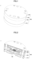
FIG. 1 is a perspective view of a force sensor device according to a first embodiment. FIG. 2 is a cross-sectional perspective view of the force sensor device according to the first embodiment. Referring to FIG. 1 and FIG. 2 , the force sensor device 1 includes a sensor chip 100 and a strain inducing body 200. The force sensor device 1 is, for example, a multi-axis force sensor device provided in an arm, a finger, or the like of a robot that is used for a machine tool or the like.
The sensor chip 100 has a function of detecting up to six axes relating to displacements in predetermined axial directions. The strain inducing body 200 has a function of transmitting at least one among an applied force and a moment, to the sensor chip 100. In the following description of embodiments, for example, a case in which the sensor chip 100 detects six axes will be described, but there is no limitation to such a sensor chip. For example, the sensor chip 100 that detects three axes or the like can be adopted.
The strain inducing body 200 includes a force receiving plate 210, a strain inducing portion 220, an input transmitter 230, and a cover plate 240. The strain inducing portion 220 is layered on the force receiving plate 210, the input transmitter 230 is layered on the strain inducing portion 220, and the cover plate 240 is layered on the input transmitter 230. The strain inducing body 200 is substantially cylindrical as a whole. The function of the strain inducing body 200 is mainly implemented by the strain inducing portion 220 and the input transmitter 230, and thus the force receiving plate 210 and the cover plate 240 may be provided as needed.
In the present embodiment, for the sake of convenience, for the force sensor device 1, the side of the cover plate 240 is referred to as a top side or one side, and the side of the force receiving plate 210 is referred to as a bottom side or another side. Further, for each component, the surface on the side of the cover plate 240 is referred to as one surface or a top surface, and the surface on the side of the force receiving plate 210 is referred to as another surface or a bottom surface. The force sensor device 1 may be used in a state of being upside down, or can be disposed at any angle. A plan view means that an object is viewed in a direction (Z-axis direction) normal to the top surface of the cover plate 240, and a planar shape refers to a shape of the object when viewed in the direction (Z-axial direction) normal to the top surface of the cover plate 240.
FIG. 3 is a perspective top view of the sensor chip attached to the input transmitter. FIG. 4 is a perspective bottom view of the sensor chip attached to the input transmitter. As illustrated in FIG. 3 and FIG. 4 , an accommodating portion that protrudes from the bottom surface of the input transmitter 230, toward the strain inducing portion 220, is provided in the input transmitter 230. The sensor chip 100 is secured to the accommodating portion 235 toward the cover plate 240.
Specifically, as described below, four second connection portions 235 c (see FIGS. 22 to 24 and the like below) each of which enters the cover plate 240 are disposed in the accommodating portion 235. The second connection portions 235 c are respectively connected to the bottom surfaces of force point portions 151 to 154 (see FIGS. 5 to 8 and the like below) of the sensor chip 100.
The accommodating portion 235 enters the strain inducing portion 220. As described below, first connection portions 224 (see FIG. 21 below), which are five columnar portions and protrude toward the input transmitter 230, are disposed in the strain inducing portion 220. The first connection portions 224 are respectively connected to bottom surfaces of the supports 101 to 105 (see FIGS. 5 to 8 and the like below) in the sensor chip 100.
The sensor chip 100 and the strain inducing body 200 will be described below in detail. In the following description, the word “parallel” is intended to include a case in which an angle between two straight lines or sides is in the range of 0°±10°. The word “vertical” or “perpendicular” is intended to include a case in which an angle between two straight lines or between sides is in the range of 90°±10°. However, when a special specification is described, it is applied. The word “center” and “middle” are intended to include an approximate center and middle of an object, and are not intended to mean only an exact center and middle. In other words, variations in manufacturing error shall be tolerable. The same applies to point symmetry and line symmetry.
(Sensor Chip 100)
FIG. 5 is a perspective view of the sensor chip 100 when viewed in the positive Z-axis direction. FIG. 6 is a plan view of the sensor chip 100 when viewed in the positive Z-axis direction. FIG. 7 is a perspective view of the sensor chip 100 when viewed in the negative Z-axis direction. FIG. 8 is a bottom view of the sensor chip 100 when viewed in the negative Z-axis direction. In FIG. 8 , for the sake of convenience, surfaces at the same height are illustrated in the same crepe pattern. In this description, a direction parallel to one side of the top surface of the sensor chip 100 refers to the X-axis direction, a direction perpendicular to the one side of the top surface of the sensor chip 100 refers to the Y-axis direction, and a thickness direction (direction normal to the top surface of the sensor chip 100) of the sensor chip 100 refers to the Z-axis direction. The X-axis direction, the Y-axis direction, and the Z-axis direction are mutually perpendicular.
The sensor chip 100 illustrated in FIGS. 5 to 8 is a microelectromechanical systems (MEMS) sensor chip that is one chip and can detect up to six axes. The sensor chip 100 is formed of a semiconductor substrate such as a silicon on insulator (SOI) substrate. The planar shape of the sensor chip 100 can be, for example, an approximate 7000 μm per side rectangle (square or rectangle).
The sensor chip 100 includes five columnar supports 101 to 105. The planar shape of each of the supports 101 to 105 can be, for example, an approximate 2000 μm per side square. The supports 101 to 104 are respectively disposed at four corners of the rectangular sensor chip 100. The support 105 is disposed on a central portion of the rectangular sensor chip 100. Each of the supports 101 to 104 is a representative example of a first support, and the support 105 is a representative example of a second support.
A frame 112 (for coupling supports that are next to each other), of which both ends are fixed by the support 101 and the support 102, is provided between the support 101 and the support 102. A frame 113 (for coupling supports that are next to each other), of which both ends are fixed by the support 102 and the support 103, is provided between the support 102 and the support 103.
A frame 114 (for coupling supports that are next to each other), of which both ends are fixed by the support 103 and the support 104, is provided between the support 103 and the support 104. A frame 111 (for coupling supports that are next to each other), of which both ends are fixed by the support 104 and the support 101, is provided between the support 104 and the support 101.
In other words, four frames 111, 112, 113, and 114 are formed as a structural frame of the sensor chip 100, and the supports 101, 102, 103, and 104 are each disposed at a corner at which given frames are coupled to each other.
An internal corner of the support 101 and a corner of the support 105 facing the internal corner of the support 101 are coupled by a coupling portion 121. An internal corner of the support 102 and a corner of the support 105 facing the internal corner of the support 102 are coupled by a coupling portion 122.
An internal corner of the support 103 and a corner of the support 105 facing the internal corner of the support 103 are coupled by a coupling portion 123. An internal corner of the support 104 and a corner of the support 105 facing the internal corner of the support 104 are coupled by a coupling portion 124.
In such a manner, the sensor chip 100 includes the coupling portions 121 to 124 each of which couples the support 105 and a given support among the supports 101 to 104. The coupling portions 121 to 124 are each disposed diagonally relative to the X-axis direction (Y-axis direction). The coupling portions 121 to 124 are respectively disposed so as not to be parallel to the frames 111, 112, 113, and 114.
The supports 101 to 105, the frames 111 to 114, and the coupling portions 121 to 124 can be each formed of, for example, an active layer, a BOX layer, and a support layer of the SOI substrate. The thickness of each of those layers can be, for example, in the range of about 400 μm to about 600 μm.
The sensor chip 100 has four sensing blocks B1 to B4. Each sensing block includes three T-patterned beam structures in each of which piezoresistive elements being strain-detecting elements are disposed. The T-patterned beam structure refers to a structure that includes a first detection beam and a second detection beam that extends from a middle portion of the first detection beam in a direction perpendicular to the first detection beam.
Specifically, the sensing block B1 includes T-patterned beam structures 131T1, 131T2, and 131T3. The sensing block B2 includes T-patterned beam structures 132T1, 132T2, and 132T3. The sensing block B3 includes T-patterned beam structures 133T1, 133T2, and 133T3. The sensing block B4 includes T-patterned beam structures 134T1, 134T2, and 134T3. The beam structure will be described below in more details.
In the sensing block B1, in a plan view, a first detection beam 131 a is provided parallel to a side of the support 104 toward the support 101 so as to be at a predetermined distance from the side of the support 104. The first detection beam 131 a extends between the frame 111, toward the support 101, and the coupling portion 121, toward the support 105. A second detection beam 131 b is provided such that one end of the second detection beam is coupled at a middle portion of the first detection beam 131 a in a longitudinal direction of the first detection beam. The second detection beam 131 b extends toward the support 104 in a direction perpendicular to the longitudinal direction of the first detection beam 131 a. The first detection beam 131 a and the second detection beam 131 b constitute the T-patterned beam structure 131T1.
In a plan view, a first detection beam 131 c is provided parallel to a side of the support 104 toward the support 101 so as to be at a predetermined distance from the side of the support 104. The first detection beam 131 c extends between the coupling portion 111, toward the support 104, and the coupling portion 124, toward the support 105. A second detection beam 131 d is provided such that one end of the second detection beam is coupled at a middle portion of the first detection beam 131 c in a longitudinal direction of the first detection beam. The second detection beam 131 d extends toward the support 101 in a direction perpendicular to the longitudinal direction of the first detection beam 131 c. The first detection beam 131 c and the second detection beam 131 d constitute the T-patterned beam structure 131T2.
In a plan view, a first detection beam 131 e is provided parallel to a side of the support 105 toward the frame 111 so as to be at a predetermined distance from the side of the support 105. The first detection beam 131 e extends between the coupling portion 121, toward the support 105, and the coupling portion 124, toward the support 105. A second detection beam 131 f is provided such that one end of the second detection beam is coupled at a middle portion of the first detection beam 131 e in a longitudinal direction, and the second detection beam 131 f extends toward the frame 111 in a direction perpendicular to the longitudinal direction of the first detection beam 131 e. The first detection beam 131 e and the second detection beam 131 f constitute the T-patterned beam structure 131T3.
Another end of the second detection beam 131 b, another end of the second detection beam 131 d, and another end of the second detection beam 131 f are connected to one another to thereby form a connection portion 141. A force point portion 151 is provided at the bottom surface of the connection portion 141. The force point portion 151 has, for example, a rectangular prismatic shape. The T-patterned beam structures 131T1, 131T2, and 131T3, the connection portion 141, and the force point portion 151 constitute the sensing block B1.
In the sensing block B1, the first detection beam 131 a, the first detection beam 131 c, and the second detection beam 131 f are parallel to one another. Also, the second detection beams 131 b and 131 d, and the first detection beam 131 e are parallel to one another. The thickness of each detection beam in the sensing block B1 can be, for example, in the range of about 30 μm to about 50 μm.
In the sensing block B2, in a plan view, a first detection beam 132 a is provided parallel to a side of the support 102 toward the support 101 so as to be at a predetermined distance from the side of the support 102. The first detection beam 132 a extends between the frame 112, toward the support 102, and the coupling portion 122, toward the support 105. A second detection beam 132 b is provided such that one end of the second detection beam is coupled at a middle portion of the first detection beam 132 a in a longitudinal direction of the first detection beam. The second detection beam 132 b extends toward the support 101 in a direction perpendicular to the longitudinal direction of the first detection beam 132 a. The first detection beam 132 a and the second detection beam 132 b constitute the T-patterned beam structure 131T2.
In a plan view, a first detection beam 132 c is provided parallel to a side of the support 101 toward the support 102 so as to be at a predetermined distance from the side of the support 101. The first detection beam 132 c extends between the frame 112, toward the support 101, and the coupling portion 121, toward the support 105. A second detection beam 132 d is provided such that one end of the second detection beam is coupled at a middle portion of the first detection beam 132 c in a longitudinal direction of the first detection beam. The second detection beam 132 d extends toward the support 102 in a direction perpendicular to the longitudinal direction of the first detection beam 132 c. The first detection beam 132 c and the second detection beam 132 d constitute the T-patterned beam structure 132T2.
In a plan view, a first detection beam 132 e is provided parallel to a side of the support 105 toward the frame 112 so as to be at a predetermined distance from the side of the support 105. The first detection beam 132 e extends between the coupling portion 122, toward the support 105, and the coupling portion 121, toward the support 105. A second detection beam 132 f is provided such that one end of the second detection beam is coupled at a middle portion of the first detection beam 132 e in a longitudinal direction, and the second detection beam 132 f extends toward the frame 111 so as to be perpendicular to the longitudinal direction of the first detection beam 132 e. The first detection beam 132 e and the second detection beam 132 f constitute the T-patterned beam structure 132T3.
Another end of the second detection beam 132 b, another end of the second detection beam 132 d, and another end of the second detection beam 132 f are connected to one another to thereby form a connection portion 142. A force point portion 152 is provided at the bottom surface of the connection portion 142. The force point portion 152 has, for example, a rectangular prismatic shape. The T-patterned beam structures 132T1, 132T2, and 132T3, the connection portion 142, and the force point portion 152 constitute the sensing block B2.
In the sensing block B2, the first detection beam 132 a, the first detection beam 132 c, and the second detection beam 132 f are parallel to one another. Also, the second detection beams 132 b and 132 d, and the first detection beam 132 e are parallel to one another. The thickness of each detection beam in the sensing block B2 may be, for example, in the range of about 30 μm to about 50 μm.
In the sensing block B3, in a plan view, a first detection beam 133 a is provided parallel to a side of the support 103 toward the support 102 so as to be at a predetermined distance from the side of the support 103. The first detection beam 133 a extends between the frame 113, toward the support 103, and the coupling portion 123, toward the support 105. A second detection beam 133 b is provided such that one end of the second detection beam is coupled at a middle portion of the first detection beam 133 a in a longitudinal direction of the first detection beam. The second detection beam 133 b extends toward the support 102 in a direction perpendicular to the longitudinal direction of the first detection beam 133 a. The first detection beam 133 a and the second detection beam 133 b constitute the T-patterned beam structure 133T1.
In a plan view, a first detection beam 133 c is provided parallel to a side of the support 102 toward the support 103 so as to be at a predetermined distance from the side of the support 102. The first detection beam 133 c extends between the frame 113, toward the support 102, and the coupling portion 122, toward the support 105. A second detection beam 133 d is provided such that one end of the second detection beam is coupled at a middle portion of the first detection beam 133 c in a longitudinal direction of the first detection beam. The second detection beam 131 d extends toward the support 103 in a direction perpendicular to the longitudinal direction of the first detection beam 133 c. The first detection beam 133 c and the second detection beam 133 d constitute the T-patterned beam structure 133T2.
In a plan view, a first detection beam 131 e is provided parallel to a side of the support 105 toward the frame 111 so as to be at a predetermined distance from the side of the support 105. The first detection beam 131 e extends between the coupling portion 121, toward the support 105, and the coupling portion 124, toward the support 105. A second detection beam 131 f is provided such that one end of the second detection beam is coupled at a middle portion of the first detection beam 131 e in a longitudinal direction, and the second detection beam 131 f extends toward the frame 111 so as to be perpendicular to the longitudinal direction of the first detection beam 131 e. The first detection beam 131 e and the second detection beam 131 f constitute the T-patterned beam structure 131T3.
Another end of the second detection beam 133 b, another end of the second detection beam 133 d, and another end of the second detection beam 133 f are connected to one another to thereby form a connection portion 143. A force point portion 153 is provided at the bottom surface of the connection portion 143. The force point portion 153 has, for example, a rectangular prismatic shape. The T-patterned beam structures 133T1, 133T2, and 133T3, the connection portion 143, and the force point portion 153 constitute the sensing block B3.
In the sensing block B3, the first detection beam 133 a, the first detection beam 133 c, and the second detection beam 133 f are parallel to one another. Also, the second detection beams 133 b and 133 d, and the first detection beam 133 e are parallel to one another. The thickness of each detection beam in the sensing block B3 may be, for example, in the range of about 30 μm to about 50 μm.
In the sensing block B4, in a plan view, a first detection beam 134 a is provided parallel to a side of the support 104 toward the support 103 so as to be at a predetermined distance from the side of the support 104. The first detection beam 134 a extends between the frame 114, toward the support 104, and the coupling portion 124, toward the support 105. A second detection beam 134 b is provided such that one end of the second detection beam is coupled at a middle portion of the first detection beam 134 a in a longitudinal direction of the first detection beam. The second detection beam 134 b extends toward the support 103 in a direction perpendicular to the longitudinal direction of the first detection beam 134 a. The first detection beam 134 a and the second detection beam 134 b constitute the T-patterned beam structure 134T1.
In a plan view, a first detection beam 134 c is provided parallel to a side of the support 103 toward the support 104 so as to be at a predetermined distance from the side of the support 103. The first detection beam 134 c extends between the frame 114, toward the support 103, and the coupling portion 123, toward the support 105. A second detection beam 134 d is provided such that one end of the second detection beam is coupled at a middle portion of the first detection beam 134 c in a longitudinal direction of the first detection beam. The second detection beam 131 d extends toward the support 104 in a direction perpendicular to the longitudinal direction of the first detection beam 134 c. The first detection beam 134 c and the second detection beam 134 d constitute the T-patterned beam structure 134T2.
In a plan view, a first detection beam 134 e is provided parallel to a side of the support 105 toward the frame 114 so as to be at a predetermined distance from the side of the support 105. The first detection beam 134 e extends between the coupling portion 124, toward the support 105, and the coupling portion 123, toward the support 105. A second detection beam 134 f is provided such that one end of the second detection beam is coupled at a middle portion of the first detection beam 134 e in a longitudinal direction, and the second detection beam 131 f extends toward the frame 114 so as to be perpendicular to the longitudinal direction of the first detection beam 134 e. The first detection beam 134 e and the second detection beam 134 f constitute the T-patterned beam structure 134T3.
Another end of the second detection beam 134 b, another end of the second detection beam 134 d, and another end of the second detection beam 134 f are connected to one another to thereby form a connection portion 144. A force point portion 154 is provided at the bottom surface of the connection portion 144. The force point portion 154 has, for example, a rectangular prismatic shape. The T-patterned beam structures 134T1, 134T2, and 134T3, the connection portion 144, and the force point portion 154 constitute the sensing block B4.
In the sensing block B4, the first detection beam 134 a, the first detection beam 134 c, and the second detection beam 134 f are parallel to one another. Also, the second detection beams 134 b and 134 d, and the first detection beam 134 e are parallel to one another. The thickness of each detection beam in the sensing block B4 may be, for example, in the range of about 30 μm to about 50 μm.
Thus, the sensor chip 100 includes the four sensing blocks (sensing blocks B1 to B4). Each sensing block is disposed in a region surrounded by (i) given supports that are next to each other and are among the supports 101 to 104, (ii) a given frame and a given coupling portion each of which couples the given supports that are next to each other, and (iii) the support 105. In a plan view, for example, given sensing blocks can be disposed to be point-symmetric with respect to the center of the sensor chip.
Each sensing block includes three T-patterned beam structures. In each sensing block, three T-patterned beam structures include two T-patterned beam structures in which, in a plan view, a given connection portion is interposed between first detection beams that are respectively included in two T-patterned beam structures and are disposed parallel to each other. The three T-beam structures also include one T-patterned beam structure including a first detection beam that is disposed parallel to second detection beams included in the respective two T-patterned beam structures. The first detection beam in the one T-patterned beam structure is disposed between the given connection portion and the support 105.
For example, in the sensing block B1, three T-patterned beam structures include T-patterned beam structures 131T1 and 131T2 in which, in a plan view, the connection portion 141 is interposed between the first detection beam 131 a and the first detection beam 131 c that are disposed parallel to each other. The three T-patterned beam structures also include the T-patterned beam structure 131T3 including the first detection beam 131 e that is disposed parallel to the second detection beams 131 b and 131 d included in the respective T-patterned beam structures 131T1 and 131T2. The first detection beam 131 e in the T-patterned beam structure 131T3 is disposed between the connection portion 141 and the support 105. The structure in each of the sensing blocks B2 to B4 is similar to that in the sensing block B1.
Each of the force point portions 151 to 154 is a point to which an external force is applied. Each force point portion can be formed of, for example, a BOX layer and a support layer in the SOI substrate. The bottom surface of each of the force point portions 151 to 154 substantially corresponds to the bottom surface of a corresponding support among the supports 101 to 105.
In such a manner, when a force or displacement is obtained through each of the four force point portions 151 to 154, a given beam deforms so as to differ according to a force type, thereby providing a sensor with greater isolation of 6 axes. The number of force point portions is the same as the number of positions of the strain inducing body to which displacements are input.
One or more internal corners of the sensor chip 100 are preferably R-shaped in order to suppress stress concentration.
The supports 101 to 105 in the sensor chip 100 are connected to a non-movable portion in the strain inducing body 200, and the force point portions 151 to 154 are connected to a movable portion of the strain inducing body 200. Even if the movable portion and non-movable portion are reversed with respect to each other, the sensor chip 100 functions as a force sensor device. That is, the supports 101 to 105 in the sensor chip 100 are connected to the movable portion of the strain inducing body 200, and the force point portions 151 to 154 may be connected to the non-movable portion of the strain inducing body 200.
FIG. 9 is a diagram for describing signs for forces and moments applied to axes. As illustrated in FIG. 9 , the force in the X-axis direction is expressed by Fx, the force in the Y-axis direction is expressed by Fy, and the force in the Z-axis direction is expressed by Fz. Also, the moment to cause rotation about the X-axis as an axis is expressed by Mx, the moment to cause rotation about the Y-axis as an axis is expressed by My, and the moment to cause rotation about the Z-axis as an axis is expressed by Mz.
FIG. 10 is a diagram illustrating the arrangement of piezoresistive elements in the sensor chip 100. FIG. 11 is an enlarged partial view of one sensing block in the sensor chip illustrated in FIG. 10 . As illustrated in FIG. 10 and FIG. 11 , piezoresistive elements are each disposed at a predetermined location of a given sensing block corresponding to a force point portion among the four force point portions 151 to 154. The arrangement of the piezoresistive elements in each of the other sensing blocks illustrated in FIG. 10 is the same as that of the piezoresistive elements in the sensing block illustrated in FIG. 11 .
Referring to FIGS. 5 to 8 , FIG. 10 , and FIG. 11 , in the sensing block B1 that includes the connection portion 141 and the force point portion 151, a piezoresistive element MzR1′ is disposed at a portion of the first detection beam 131 a that is toward the second detection beam 131 b and is between the second detection beam 131 b and the first detection beam 131 e. A piezoresistive element FxR3 is disposed at a portion of the first detection beam 131 a that is toward the first detection beam 131 e and is between the second detection beam 131 b and the first detection beam 131 e. A piezoresistive element MxR1 is disposed on the second detection beam 131 b toward the connection portion 141.
A piezoresistive element MzR2′ is disposed at a portion of the first detection beam 131 c that is toward the second detection beam 131 d and is between the second detection beam 131 d and the first detection beam 131 e. A piezoresistive element FxR1 is disposed at a portion of the first detection beam 131 c that is toward the first detection beam 131 e and is between the second detection beam 131 d and the first detection beam 131 e. A piezoresistive element MxR2 is disposed on the second detection beam 131 d toward the connection portion 141.
A piezoresistive element FzR1′ is disposed on the second detection beam 131 f toward the connection portion 141. A piezoresistive element FzR2′ is disposed on the second detection beam 131 f toward the first detection beam 131 e. The piezoresistive elements MzR1′, FxR3, MxR1, MzR2′, FxR1, and MxR2 are each disposed at a location apart from a middle portion of a corresponding detection beam in a longitudinal direction.
In the sensing block B2 that includes the connection portion 142 and the force point portion 152, a piezoresistive element MzR4 is disposed at a portion of the first detection beam 132 a that is toward the second detection beam 132 b and is between the second detection beam 132 b and the first detection beam 132 e. A piezoresistive element FyR3 is disposed at a portion of the first detection beam 132 a that is toward the first detection beam 132 e and is between the second detection beam 132 b and the first detection beam 132 e. A piezoresistive element MyR4 is disposed on the second detection beam 132 b toward the connection portion 142.
A piezoresistive element MzR3 is disposed at a portion of the first detection beam 132 c that is toward the second detection beam 132 d and is between the second detection beam 132 d and the first detection beam 132 e. A piezoresistive element FyR1 is disposed at a portion of the first detection beam 132 c that is toward the first detection beam 132 e and is between the second detection beam 132 d and the first detection beam 132 e. A piezoresistive element MyR3 is disposed on the second detection beam 132 d toward the connection portion 142.
A piezoresistive element FzR4 is disposed on the second detection beam 132 f toward the connection portion 142. A piezoresistive element FzR3 is disposed on the second detection beam 132 f toward the first detection beam 132 e. The piezoresistive elements MzR4, FxR3, MyR4, MzR3, FyR1, and MyR3 are each disposed at a location apart from a middle portion of a corresponding detection beam in a longitudinal direction.
In the sensing block B3 that includes the connection portion 143 and the force point portion 153, a piezoresistive element MzR4′ is disposed at a portion of the first detection beam 133 a that is toward the second detection beam 133 b and is between the second detection beam 133 b and the first detection beam 133 e. A piezoresistive element FxR2 is disposed at a portion of the first detection beam 133 a that is toward the first detection beam 133 e and is between the second detection beam 133 b and the first detection beam 133 e. A piezoresistive element MxR4 is disposed on the second detection beam 133 b toward the connection portion 143.
A piezoresistive element MzR3′ is disposed at a portion of the first detection beam 133 c that is toward the second detection beam 133 d and is between the second detection beam 133 d and the first detection beam 133 e. A piezoresistive element FxR4 is disposed at a portion of the first detection beam 133 c that is toward the first detection beam 133 e and is between the second detection beam 133 d and the first detection beam 133 e. A piezoresistive element MxR3 is disposed on the second detection beam 133 d toward the connection portion 143.
A piezoresistive element FzR4′ is disposed on the second detection beam 133 f toward the connection portion 143. A piezoresistive element FzR3′ is disposed on the second detection beam 133 f toward the first detection beam 133 e. The piezoresistive elements MzR4′, FxR2, MxR4, MzR3′, FxR4, and MxR3 are each disposed at a location apart from a middle portion of a corresponding detection beam in a longitudinal direction.
In the sensing block B4 that includes the connection portion 144 and the force point portion 154, a piezoresistive element MzR1 is disposed at a portion of the first detection beam 134 a that is toward the second detection beam 134 b and is between the second detection beam 134 b and the first detection beam 134 e. A piezoresistive element FyR2 is disposed at a portion of the first detection beam 134 a that is toward the first detection beam 134 e and is between the second detection beam 134 b and the first detection beam 134 e. A piezoresistive element MyR1 is disposed on the second detection beam 132 b toward the connection portion 144.
A piezoresistive element MzR2 is disposed at a portion of the first detection beam 134 c that is toward the second detection beam 134 d and is between the second detection beam 134 d and the first detection beam 134 e. A piezoresistive element FyR4 is disposed at a portion of the first detection beam 134 c that is toward the first detection beam 134 e and is between the second detection beam 134 d and the first detection beam 134 e. A piezoresistive element MyR2 is disposed on the second detection beam 134 d toward the connection portion 144.
A piezoresistive element FzR1 is disposed on the second detection beam 134 f toward the connection portion 144. A piezoresistive element FzR2 is disposed on the second detection beam 134 f toward the first detection beam 134 e. The piezoresistive elements MzR1, FxR2, MyR3, MyR1, FzR2, and MyR2 are each disposed at a location apart from a middle portion of a corresponding detection beam in a longitudinal direction.
In such a manner, in the sensor chip 100, each of the sensing blocks individually includes multiple piezoresistive elements. With this arrangement, when inputs are respectively applied to the force point portions 151 to 154, the sensor chip 100 can detect up to six axes relating to forces in predetermined axis-directions or moments about respective predetermined axes, based on changes in the outputs of multiple piezoresistive elements on given beams.
In addition to the piezoresistive elements used to detect strain, one or more dummy piezoresistive elements may be disposed in the sensor chip 100. The dummy piezoresistive elements are used to adjust variations in stress against detection beams or resistance of a bridge circuit. For example, all piezoresistive elements including piezoresistive elements used to detect strain are arranged so as to be point-symmetrical with respect to the center of the support 105.
In the sensor chip 100, each piezoresistive element among multiple piezoresistive elements to detect the displacement in the X-axis direction and the displacement in the Y-axis direction is disposed on the first detection beam included in a given T-patterned beam structure, and further, each piezoresistive element among multiple piezoresistive elements to detect the displacement in the Z-axis direction is disposed on the second detection beam included in a given T-patterned beam structure. Furthermore, each piezoresistive element among multiple piezoresistive elements to detect moments about the Z-axis direction is disposed on the first detection beam included in a given T-patterned beam structure, and further, each piezoresistive element among multiple piezoresistive elements to detect moments about the X-axis direction and the Y-axis direction is disposed on the second detection beam included in a given T-patterned beam structure.
Each of the piezoresistive elements FxR1 to FxR4 detects the force Fx, each of the piezoresistive elements FyR1 to FyR4 detects the force Fy, and each of the piezoresistive elements FzR1 to FzR4 and FzR1′ to FzR4′ detects the force Fz. Also, each of the piezoresistive elements MxR1 to MxR4 detects the moment Mx, each of the piezoresistive elements MyR1 to MyR4 detects the moment My, and each of the piezoresistive elements MzR1 to MzR4 and MzR1′ to MzR4′ detects the moment Mz.
In such a manner, in the sensor chip 100, each of the sensing blocks individually includes multiple piezoresistive elements. With this arrangement, when forces or displacements are respectively applied (transmitted) to the force point portions 151 to 154, the sensor chip 100 can detect up to six axes relating to forces in predetermined directions or moments about the respective directions (axis-directions), based on changes in the outputs of multiple piezoresistive elements on given beams. By changing the thickness and width of each detection beam, equalization of detection sensitivity, increases in detection sensitivity, or the like can be controlled.
By reducing the number of piezoresistive elements, a sensor chip for detecting five axes or less relating to displacements in predetermined axis directions can be provided.
In the sensor chip 100, for example, a detecting circuit described below can be used to detect forces and moments. Each of FIG. 12 and FIG. 13 illustrates an example of the detecting circuit that uses piezoresistive elements. In each of FIG. 12 and FIG. 13 , numbers rounded with squares indicate external output terminals. For example, the number “1” indicates a power supply terminal for a Fx-axis, a Fy-axis, and a Fz-axis. The number “2” is a negative output terminal for the Fx-axis. The number “3” indicates a GND terminal for the Fx-axis, and the number “4” indicates a positive output terminal for the Fx-axis. The number “19” indicates a negative output terminal for the Fy-axis, the number “20” indicates a GND terminal for the Fy-axis, and the number “21” indicates a positive output terminal for the Fy-axis. The number “22” indicates a negative output terminal for the Fz-axis, the number “23” indicates a GND terminal for the Fz-axis, and the number “24” indicates a positive output terminal for the Fz-axis.
The number “9” indicates a negative terminal for the Mx-axis, the number “10” indicates a GND terminal for the Mx-axis, and the number “11” indicates a positive output terminal for the Mx-axis. The number “12” indicates a power supply terminal for the Mx-axis, My-axis, and Mz-axis. The number “13” indicates a negative output terminal for the My-axis, the number “14” indicates a GND terminal for the My-axis, and the number “15” indicates a positive output terminal for the My-axis. The number “16” indicates a negative output terminal for the Mz-axis, the number “17” indicates a GND terminal for the Mz-axis, and the number “18” indicates a positive output terminal for the Mz-axis.
Hereafter, deformation of the detection beam will be described. FIG. 14 is a diagram describing an input Fx. FIG. 15 is a diagram for describing an input Fy. As illustrated in FIG. 14 , when the input from the strain inducing body 200 to which the sensor chip 100 is attached is expressed by Fx, all of the four force point portions 151 to 154 attempt to move in the same direction (rightward direction in an example in FIG. 14 ). Similarly, as illustrated in FIG. 15 , when the input from the strain inducing body 200 to which the sensor chip 100 is attached is expressed by Fy, all four force point portions 151 to 154 attempt to move in the same direction (upward direction in an example in FIG. 15 ). In this case, although the sensor chip 100 includes four sensing blocks, the respective force point portions in all sensing blocks move in the same direction, in accordance with displacements in the X-axis direction and Y-axis direction.
FIG. 16 is a diagram illustrating a simulation result obtained when the sensor chip receives the input Fx. When the inputs Fx expressed by the arrows in FIG. 14 are applied, detection beams deform as illustrated in FIG. 16 . In particular, it can be seen that one or more first detection beams (one or more beams in a lateral position in a given T-patterned beam structure) is greatly deformed in each sensing block.
In the sensor chip 100, each T-patterned beam structure includes one or more first detection beams that are among all first detection beams in a given T-patterned beam structure and are perpendicular to a displacement direction of the input. With this arrangement, such first detection beams perpendicular to the displacement direction of the input can deform greatly, as illustrated in FIG. 16 . In FIG. 16 , the first detection beams, which are perpendicular to the displacement direction of the input, include the first detection beams 131 a, 131 c, 132 e, 133 a, 133 c, and 134 e illustrated in FIG. 6 and the like.
Beams used to detect the inputs Fx include the first detection beams 131 a, 131 c, 133 a, and 133 c. Each beam among those beams is a first detection beam in a given T-patterned beam structure, and is at a fixed distance from a given force point portion. The beams used to detect the inputs Fy include the first detection beams 132 a, 132 c, 134 a, and 134 c. Each beam among those beams is a first detection beam in a given T-patterned beam structure, and is at a distance from a given force point portion.
In response to inputs Fx and the inputs Fy, first detection beams, on which the piezoresistive elements are disposed and that are each included in a given T-patterned beam structure, deform greatly, thereby effectively detecting the input forces. Also, beams not used to detect the inputs are designed to be greatly deformable in accordance with the displacement occurring when the inputs Fx and Fy are applied. With this arrangement, even if at least one input among the input Fx and the input Fy is increased, none of the detection beams are broken.
Conventional sensor chips include beams not being able to deform greatly in accordance with at least one given input among the inputs Fx and the inputs Fy. Thus, when at least one input among the input Fx and the input Fy is increased, the beams not being deformed might be broken. The sensor chip 100 can address the issue described above. That is, the sensor chip 100 can have increased fracture resistance of beams, even when displacements in various directions occur.
As described above, the sensor chip 100 includes one or more first detection beams perpendicular to the displacement direction of each input, and the one or more first detection beams perpendicular to the displacement direction can greatly deform. With this arrangement, the input Fx and the input Fy can be effectively detected. Also, even if at least one input among the input Fx and the input Fy is increased, none of the detection beams are broken. As a result, the sensor chip 100 can be used for any increased rating capacity, and a measurement range and load bearing can be also improved. For example, the sensor chip 100 may have a rating capacity of 500N, which is about 10 times greater than that of conventional chips.
In each sensing block, beams each extending in three directions in a given T-patterned beam structure are coupled to one another at a given force point portion, and deform so as to differ according to inputs. Thus, multi-axial forces can be detected more separately.
When beams are arranged in the T pattern, an increased number of paths that are each from a given beam to either a given frame or a given coupling portion is obtained. With this arrangement, a line is easily drawn to the outer periphery of the sensor chip. Therefore, layout flexibility can be improved.
FIG. 17 is a simulation result when the input Mz is applied to the sensor chip. As illustrated in FIG. 17 , for given two first detection beams, between which a given force point portion is disposed and that are among the first detection beams 131 a, 131 c, 132 a, 132 c, 133 a, 133 c, 134 a, and 134 c, the given first detection beams greatly deform in response to the moment about the Z-axis direction. With this arrangement, piezoresistive elements can be disposed on some or all of the first detection beams.
FIG. 18 is a simulation result when the input Fz is applied to the sensor chip. FIG. 19 is a partial perspective view of the sensor chip illustrated in FIG. 18 . As illustrated in FIG. 18 and FIG. 19 , for given two second detection beams, which are directly connected to a given force point portion and are among the second detection beams 131 b, 131 d, 131 f, 132 b, 132 d, 132 f, 133 b, 133 d, 133 f, 134 b, 134 d, and 134 f, the given two second detection beams mainly deform greatly in response to the displacement in the Z-axis direction. With this arrangement, piezoresistive elements can be disposed on some or all of the second detection beams.
(Strain Inducing Body 200)
As illustrated in FIG. 1 and FIG. 2 , the strain inducing body 200 includes the force receiving plate 210, the strain inducing portion 220, the input transmitter 230, and the cover plate 240. Each component of the strain inducing body 200 will be described below.
FIG. 20 is a perspective view of the force receiving plate included in the strain inducing body. As illustrated in FIG. 20 , the force receiving plate 210 is a member that is substantially disk-shaped as a whole and receives the force and moment from a target object to be measured. The force receiving plate 210 includes an outer frame 211 that is substantially ring-shaped in a plan view, and includes a central portion 212 that is apart from the outer frame 211 and is disposed inside the outer frame 211, where the central portion 212 is substantially circular in a plan view. The force receiving plate 210 also includes multiple beam structures 213 each of which couples the outer frame 211 and the central portion 212. Even when the beam structure 213 causes increases in strength of the force receiving plate 210, and the force or moment is received through the target object, deformation of the force receiving plate 210 itself is negligible. With this arrangement, without the losses in the deformation (displacement), the force or moment is transmitted to the strain inducing portion 220 that is connected to the central portion 212. Through-holes 218 are each provided in a portion of the force receiving plate 210 that extends from the inside of the outer frame 211 toward each beam structure 213. The through-holes 218 can be used for, for example, screwing the force receiving plate 210 into the target object.
FIG. 21 is a perspective view of the strain inducing portion included in the strain inducing body. As illustrated in FIG. 21 , the strain inducing portion 220 is a substantially disk-shaped member as a whole, and deforms in response to receiving the force from the force receiving plate 210.
The strain inducing portion 220 includes an outer frame 221 that is substantially ring-shaped in a plan view, and includes a central portion 222 that is apart from the outer frame 221 and is disposed inside the outer frame 221, where the central portion 222 is substantially circular in a plan view. The strain inducing portion 220 also includes multiple beam structures 223 each of which couples the outer frame 221 and the central portion 222. For example, given beam structures are disposed so as to be point-symmetric with respect to the center of the strain inducing portion 220. The number of beam structures 223 is, for example, four. For example, each beam structure 223 includes a first beam and a second beam that extends from a middle portion of the first beam in a direction perpendicular to the first beam, where the first beam and the second beam are arranged in a T pattern. Both ends of the first beam are coupled to the outer frame 221, and one end of the second beam is coupled to the central portion 222.
The central portion 222 is formed to be thinner than the outer frame 221, and each beam structure 223 is further thinner than the central portion 222. The top surface of the central portion 222 and the top surface of each beam structure 223 are approximately the same plane and are located lower than the top surface of the outer frame 221. The bottom surface of the central portion 222 protrudes slightly from the bottom surface of the outer frame 221. The bottom surface of each beam structure 223 is located higher than the bottom surface of the outer frame 221 and the bottom surface of the central portion 222. Only the beam structures 223 and the central portion 222 deform in response to receiving the force from the force receiving plate 210, and the outer frame 221 does not deform. Although the central portion 222 moves in accordance with the deformation of each beam structure 223, the central portion 222 itself does not deform.
A groove 220 x is formed at the surface of the central portion 222 toward the input transmitter 230. The shape of the groove 220 x is a shape in which, in a plan view, a square groove portion overlaps with a cross-shaped groove portion that includes two elongated groove portions that are each longer than one side of the square groove portion and are perpendicular to each other. The depth of the square groove portion is the same as that of each cross-shaped groove portion.
First connection portions 224, which include five columnar portions each protruding toward the input transmitter 230, are respectively disposed at (i) four corners of the square groove portion other than the cross-shaped groove portion, and (ii) the center of the square groove portion. In this case, the first connection portions 224 do not contact an inner wall of the groove 220 x. Each first connection portion 224 is a portion connected to a given support among the supports 101 to 105 in the sensor chip 100. The top surface of each first connection portion 224 is approximately in the same plane and is located lower than the top surface of the central portion 222 and the top surfaces of the beam structures 223. Through-holes 228 are provided in the outer frame 221. For example, with use of screws, the through-holes 228 can be used to secure the strain inducing portion 220, the input transmitter 230, and the cover plate 240, to a fixed side (a robot-side or the like).
A space is provided toward the top surface of the central portion 222. For example, a circuit board or the like that includes electronic components such as a connector and a semiconductor element may be disposed on the top surface of the central portion 222 so as not to enter the top surface of the outer frame 221.
FIG. 22 is a perspective top view of the input transmitter included in the strain inducing body. FIG. 23 is a perspective bottom view of the input transmitter included in the strain inducing body. FIG. 24 is a side view of the input transmitter included in the strain inducing body. As illustrated in FIGS. 22 to 24 , the input transmitter 230 is a member that is substantially disk-shaped as a whole and transmits deformation (input) of the strain inducing portion 220 to the sensor chip 100.
The input transmitter 230 includes an outer frame 231 that is substantially ring-shaped in a plan view, and includes a central portion 232 that is apart from the outer frame 231 and is disposed inside the outer frame 231. The input transmitter 230 also includes multiple beam structures 233 each of which couples the outer frame 231 and the central portion 232. For example, given beam structures are disposed so as to be point-symmetric with respect to the center of the input transmitter 230. The number of beam structures 233 is, for example, four. Each beam structure 233 is, for example, I-shaped.
The central portion 232 includes an inner frame 234 that is substantially ring-shaped in a plan view and is connected to each of the beam structures 233. The central portion 232 also includes an accommodating portion 235 that is substantially cross-shaped in a plan view that extends from the bottom surface of the inner frame 234 toward the strain inducing portion 220. The accommodating portion 235 includes four vertical supports 235 a each of which extends vertically from the bottom surface of the inner frame 234 toward the strain inducing portion 220. The accommodating portion 235 also includes four horizontal supports 235 b each of which extends horizontally from the bottom end of a given vertical support 235 a and is coupled at the center of the inner frame 234.
The beam structures 233 and the inner frame 234 are each formed to be thinner than the outer frame 231. The top surfaces of the beam structures 233 and the inner frame 234 are each disposed lower than the top surface of the outer frame 231. The bottom surface of the outer frame 231, the bottom surfaces of the beam structures 233, and the bottom surface of the inner frame 234 are substantially in the same plane. The input transmitter 230 does not deform even when any component of the input transmitter 230 receives the force or moment.
In a plan view, given vertical supports among the four vertical supports 235 a are disposed so as to be point-symmetric with respect to the center of the input transmitter 230, and given horizontal supports among the four horizontal supports 235 b are disposed so as to be point-symmetric with respect to the center of the input transmitter 230. In a plan view, the longitudinal direction of each horizontal supports 235 b is not the same as the longitudinal direction of a corresponding beam structure 233. For example, in a plan view, the longitudinal direction of each horizontal support 235 b and the longitudinal direction of a corresponding beam structure 233 are disposed at an offset by 45 degrees.
Grooves 235 x are provided near the center of the substantially cross-shaped accommodating portion 235, and the bottom surface of each groove 235 x is arranged such that a corresponding second connection portion 235 c protruding toward the cover plate 240 does not contact the inner wall of the groove 235 x. Each second connection portion 235 c is substantially located on a line that is determined by bisecting a corresponding horizontal support 235 b in the longitudinal direction. Each second connection portion 235 c is a portion connected to a given force point portion among the force point portions 151 to 154 in the sensor chip 100. Through-holes 238 are provided in the outer frame 231. The through-holes 238 can be used to, for example, screw the strain inducing portion 220, the input transmitter 230, and the cover plate 240, into the fixed side (robot-side or the like).
A space is provided toward the top surface of each beam structure 233. For example, a circuit board or the like that includes electronic components such as a connector and a semiconductor element may be disposed on the top surface of the each beam structure 233 so as not to enter the top surface of the outer frame 221.
FIG. 25 is a perspective view of the cover plate included in the strain inducing body. As illustrated in FIG. 25 , the cover plate 240 is a disk-like member as a whole and protects internal components (the sensor chip 100 and the like). The cover plate 240 is formed to be thinner than the force receiving plate 210, the strain inducing portion 220, and the input transmitter 230. Through-holes 248 are provided in the cover plate 240. For example, the through-holes 248 can be used to screw the strain-inducing portion 220, the input transmitter 230, and the cover plate 240, to the fixed side (robot-side or the like).
For example, a hard metallic material, such as SUS (stainless steel), can be used as the material of each of the force receiving plate 210, the strain inducing portion 220, the input transmitter 230, and the cover plate 240. In this regard, it is preferable to use stainless steel of SUS 630 specified by the Japanese industrial standards (JIS). Such stainless steel is hard and has increased mechanical strength. For components included in the strain inducing body 200, it is desirable for the force receiving plate 210, the strain inducing portion 220, and the input transmitter 230 to be firmly connected to one another, or to be integrally configured. As a method of connecting the force receiving plate 210, the strain inducing portion 220, and the input transmitter 230, fastening may be performed with screws. Alternatively, welding or the like may be performed. In any case, those components of the strain inducing body 200 need to sufficiently withstand the force and moment that is input to the strain inducing body 200.
In the present embodiment, for example, the force receiving plate 210, the strain inducing portion 220, and the input transmitter 230 are each fabricated by injection molding that uses metal powder, and then sintering of these fabricated components that are layered is again performed so that they are diffusion-welded. The force receiving plate 210, the strain inducing portion 220, and the input transmitter 230 that are diffusion-welded have necessary and sufficient welding strength. The cover plate 240 may be fastened to the input transmitter 230 by, for example, one or more screws, after mounting of the sensor chip 100 and other internal components.
When the force or moment is applied to the force receiving plate 210 in the strain inducing body 200, the force or moment is transmitted to the central portion 222 of the strain inducing portion 220 connected to the force receiving plate 210, and thus each of four beam structures 223 deforms in response to receiving a given input. In this case, the outer frame 221 and the input transmitter 230 in the strain inducing portion 220 do not deform.
In such a manner, in the strain inducing body 200, each of the force receiving plate 210, the central portion 222 of the strain inducing portion 220, and the beam structures 223 is a movable portion that deforms in response to receiving a predetermined axial force or moment about a predetermined axis. The outer frame 221 of the strain inducing portion 220 is a non-movable portion that does not deform in response to receiving the force or moment. The input transmitter 230, which is joined to the outer frame 221, as a non-movable portion, of the strain inducing portion 220, is a non-movable portion that does not deform in response to receiving the force or moment. Likewise, the cover plate 240, which is joined to the input transmitter 230, is a non-movable portion that does not deform in response to the force or moment.
When the strain inducing body 200 is used in the force sensor device 1, the supports 101 to 105 of the sensor chip 100 are respectively connected to the first connection portions 224 provided on the central portion 222 that is a movable portion. Also, the force point portions 151 to 154 of the sensor chip 100 are respectively connected to the second connection portions 235 c that are provided in the accommodating portion 235, which is a non-movable portion. With this arrangement, the sensor chip 100 operates such that detection beams deform through the respective supports 101 to 105, without the movement of the force point portions 151 to 154.
In another example, the strain inducing body 200 may be configured, such that the force point portions 151 to 154 of the sensor chip 100 are respectively connected to the first connection portions 224 that are provided at the central portion 222, which is a movable portion and such that the supports 101 to 105 of the sensor chip 100 are respectively connected to the second connection portions 235 c that are provided in the accommodating portion 235, which is a non-movable portion.
In such a case, the sensor chip 100 that can be accommodated in the accommodating portion 235 includes the supports 101 to 105 and the force point portions 151 to 154, where the positional relationship between supports, as well as the positional relationship between force point portions, change in response to receiving a force or moment. In the strain inducing body 200, the central portion 222 that is a movable portion includes first connection portions 224 each of which extends toward the input transmitter 230 and is connected to both a given support among the supports 101 to 105 and one end of a given force point portion among the force points 151 to 154. The accommodating portion 235 includes second connection portions 235 c each of which is connected to both the given support among the support 101 to 105 and another end of the given force portion among the force point portions 151 to 154.
FIG. 26 is a diagram illustrating a simulation result when the input Fx is applied to the strain inducing portion. FIG. 27 is a diagram illustrating a simulation result when the input Mz is applied to the strain inducing portion. As illustrated in FIG. 26 and FIG. 27 , it can be seen in both cases that four T-patterned beam structures 223 are deformed without the outer frame 221 of the strain inducing portion 220 being deformed. The same applies to a case where other inputs are applied.
With this arrangement, the strain inducing body 200 converts the input force or moment to a given displacement to thereby transmit it to the sensor chip 100 that is provided in the strain inducing body 200. In conventional strain inducing bodies that have similar functions, a structure that receives forces and moments, as well as a structure that transmits displacements, are integrally configured or closely coupled to each other. For this reason, there is an increased trade-off between the displacement and load bearing and consequently it is particularly difficult to increase the load bearing.
In the strain inducing body 200, the strain inducing portion 220 that receives forces and moments, as well as the input transmitter 230 that transmits the displacement to the sensor chip 100, are formed as separate structures. With this arrangement, displacement can be appropriately detected, while increasing load bearing.
First Modification of the First Embodiment
A first modification of the first embodiment illustrates an example of the sensor chip having a different structure from that of the sensor chip described in the first embodiment. In the first modification of the first embodiment, description for the same configuration that has been the same as that in the above embodiments may be omitted.
FIG. 28 is a plan view of a sensor chip 100A when viewed in the positive Z-axis direction. As illustrated in FIG. 28 , the sensor chip 100A has a detection beam structure as in the structure of the sensor chip 100 (see FIG. 6 and the like). However, a space shape defined in the surroundings of each detection beam differs from that defined in the sensor chip 100. In other words, in the sensor chip 100A, opening widths of spaces provided at both sides of each detection beam are the same in a plan view.
In general, beam structures of sensor chips are formed using a silicon wafer in a semiconductor process, where a deep etch is performed by dry etching. If some opening widths in etched regions that are separated by detection beams are greater and are not the same, as in those determined in the shape of the sensor chip 100, it might be more difficult to process the wafer, thereby resulting in reductions in processing quality.
In the sensor chip 100A, an elongated etching region having the same opening width is formed over both sides of each detection beam. With this arrangement, when a deep etch is performed by dry etching, processing difficulty is reduced, thereby increasing processing quality. In FIG. 28 , four circular openings are undercuts used to cause the sensor chip 100A to prevent the contact with the strain inducing body 200, when the sensor chip 100A is attached to the strain inducing body 200. If only efficiency in dry etching is considered, the four circular openings may not be provided.
FIG. 29 is a partial plan view of a sensor chip 100B when viewed in the positive Z-axis direction. As illustrated in FIG. 29 , the sensor chip 100B differs from the sensor chip 100 (see FIG. 6 and the like) in that one ends of respective second detection beams included in two T-patterned beam structures are connected to each other each at one end in the sensing block B1. In the sensor chip 100, respective second detection beams included in three T-patterned beam structures are connected to one another each at one end. In contrast to the sensor chip 100, the sensor chip 100B does not include first detection beams 131 e, 132 e, 133 e, and 134 e, as well as second detection beams 131 f, 132 f, 133 f, and 134 f. The structure in each of sensing blocks B2 to B4 is the same as that in the sensing block B1.
FIG. 30 is a partial plan view of a sensor chip 100C when viewed from the positive Z-axis direction. As illustrated in FIG. 30 , the sensor chip 100C differs from the sensor chip 100 (see FIG. 6 and the like) in that respective second detection beams included in four T-patterned beam structures are connected to one another each at one end in the sensing block B1. In the sensor chip 100, respective second detection beams in three T-patterned beam structures are connected to one another each at one end. In contrast to the sensor chip 100, the sensor chip 100C further includes a T-patterned beam structure 131T4 that includes a first detection beam 131 g and a second detection beam 131 h. The T-patterned beam structure 131T4 is disposed such that the connection portion 141 is interposed between the T-patterned beam structure 131T3 and the T-patterned beam structure 131T4. The structure in each of sensing blocks B2 to B4 is the same as that in the sensing block B1.
As described above, the T-patterned beam structure is not limited to having three beams in a given sensor chip. The T-patterned beam structure may include two beams as in the sensor chip 100B. Alternatively, the T-patterned beam structure may include four beams as in the sensor chip 100C. In both cases, when each sensing block includes two or more T-patterned beam structures, one or more first detection beams or one or more second detection beams included in a given T-patterned beam structure can greatly deform. With this arrangement, at least one input among the input Fx and the input Fy can be detected effectively. Further, even if one input among the input Fx and the input Fy is increased, any detection beams are not broken. That is, in any sensor chip, fracture resistance of beams with respect to displacements in various directions can be improved. Therefore, the sensor chip can be used for increased rating capacity, as well as having an increased measurement range and load bearing.
When two T-patterned beam structures are used, it is difficult to detect displacements in 6-axis directions. When the number of T-patterned beam structures is increased, it is advantageous in that it is easier to isolate forces of multiple axes. However, the chip size may be likely to be increased. In view of the point described above, it is preferable to use three T-patterned beam structures in order to detect displacements in the 6-axis directions.
Second Modification of the First Embodiment
A second modification of the first embodiment illustrates an example of the strain inducing body having a different structure from that in the first embodiment. In the second modification of the first embodiment, description for the same configuration that has been described in the above embodiments may be omitted.
FIG. 31 is a perspective view of a strain inducing body 200A. FIG. 32 is a cross-sectional perspective view of the strain inducing body 200A. Referring to FIG. 31 and FIG. 32 , the strain inducing body 200A includes the force receiving plate 210, the strain inducing portion 220, an input transmitter 230A, and a cover plate 240A. The strain inducing portion 220 is layered on the force receiving plate 210, and the input transmitter 230A is layered on the strain inducing portion 220. The cover plate 240A is layered on the input transmitter 230A. With this arrangement, the strain inducing portion 200A is formed to be substantially cylindrical as a whole. The central portion of the cover plate 240A can be opened and closed by an inner lid portion 241. The force receiving plate 210 and the strain inducing portion 220 are configured as in the strain inducing body 200.
FIG. 33 is a perspective top view of the input transmitter included in the strain inducing body. As illustrated in FIG. 33 , the input transmitter 230A has the same basic structure as that of the input transmitter 230. However, the input transmitter 230A is formed to be thinner than the input transmitter 230.
FIG. 34 is a perspective view of the cover plate included in the strain inducing body. As illustrated in FIG. 34 , the cover plate 240A is a member that is substantially disk-shaped as a whole and protects internal components (the sensor chip 100 and the like). For example, the cover plate 240A is formed to be thicker than the force receiving plate 210, the strain inducing portion 220, and the input transmitter 230A, and has a wide internal space toward the input transmitter 230A. The cover plate 240A has through- holes 248 and 249. The through-hole 249 is closed by the inner lid portion 241 (see FIG. 31 ).
As described above, a boundary between given components included in the strain inducing body can be changed in consideration of (i) an internal space provided in the strain inducting body, (ii) an assembling level, and (iii) the like. In the example illustrated in FIGS. 31 to 34 , the boundary between the input transmitter and the cover plate is changed in comparison to the case illustrated in FIG. 1 and the like. In this case, a wide internal space toward the cover plate 240A can be provided and thus more components can be incorporated in the space.
Third Modification of the First Embodiment
A third modification of the first embodiment illustrates another example of the strain inducing body having a different structure from that described in the first embodiment. In the third modification of the first embodiment, description for the configuration that is the same as that described in the above embodiments may be omitted.
FIG. 35 is a side view of a strain inducing body 200B. Referring to FIG. 35 , the strain inducing body 200B includes the force receiving plate 210, a strain inducing portion 220B, the input transmitter 230, and the cover plate 240. The strain inducing portion 220B is layered on the force receiving plate 210, the input transmitter 230 is layered on the strain inducing portion 220B, and the cover plate 240 is layered on the input transmitter 230. With this arrangement, the strain inducing portion 200B is formed to be substantially cylindrical as a whole. The force receiving plate 210, the input transmitter 230, and the cover plate 240 are configured as in the strain inducing body 200.
FIG. 36 is a perspective bottom view of the strain inducing portion included in the strain inducing body. In FIG. 36 , the strain inducing portion 220B is inverted up-down from FIG. 35 . As illustrated in FIG. 35 and FIG. 36 , the strain inducing portion 220B has a protrusion 225 that protrudes toward the force receiving plate 210. The protrusion 225 is substantially circular in a plan view and is configured to be in contact with the central portion 212 of the force receiving plate 210. A protruding amount of the protrusion 225 from the bottom surface of the strain inducing portion 220B is, for example, about 0.5 mm. The protrusion 225 is bonded to the central portion 212 of the force receiving plate 210, by, for example, diffusion bonding. However, fastening may be performed with screws, or welding may be performed. After the strain inducing portion 220B and the force receiving plate 210 are bonded to each other, a space provided between the strain inducing portion 220B and the force receiving plate 210 is defined by the height of the protrusion 225.
A space needs to be provided between the strain inducing portion 220B and the force receiving portion 210, in order for the force receiving portion 210 to deform in response to receiving a force. By providing the protrusion 225 in the strain inducing portion 220B, the space can be easily provided between the force receiving portion 210 and the strain inducing portion 220B, in the strain inducing body 200B. That is, by providing the protrusion 225 in the strain inducing portion 220B, the height of the protrusion 225 can be adjusted, and thus the space between the strain inducing portion 220B and the force receiving plate 210 can be adjusted. For example, if the height of the protrusion 225 is precisely adjusted by polishing or the like, prior to bonding of the strain inducing portion 220B and the force receiving plate 210, the space provided after the bonding can be adjusted as appropriately. Further, in a method of providing the protrusion 225 in the strain inducing portion 220B, a narrow space, which is difficult to form by machining such as bonding or wire cutting, can be formed. When the strain inducing portion 220B and the force receiving plate 210 are bonded by diffusion bonding, bonding strength corresponding to material strength is obtained.
The protrusion may be provided on the side of the force receiving plate 210. Alternatively, protrusions may be respectively provided on both the strain inducing portion 220B and the force receiving plate 210. In any case, one or more protrusions are provided between the strain inducing portion 220B and the force receiving plate 210, and function as a space-defining portion for defining a given space between the strain inducing portion 220B and the force receiving plate 210.
Although the preferred embodiments have been described in detail above, various modifications and substitutions can be made to the embodiments described above without departing from the scope defined in the present disclosure.

Claims (14)

What is claimed is:
1. A strain inducing body comprising:
a strain inducing portion, the strain inducing portion including
a movable portion configured to receive a force in a predetermined axial direction or a moment about the predetermined axial direction and to deform in accordance with the received force or moment, and
a non-movable portion configured to receive the force or moment and to not deform in accordance with the received force or moment, and
an input transmitter coupled to the non-movable portion and including an accommodating portion for accommodating a sensor chip configured to detect the force or moment, the input transmitter being configured to:
receive the force or moment and to not deform in accordance with the received force or moment, and
transmit deformation of the strain inducing portion to the sensor chip,
wherein the strain inducing portion and the input transmitter are vertically stacked.
2. The strain inducing body according to claim 1, wherein the sensor chip includes a first portion and a second portion, a positional relationship between the first portion and the second portion changing with occurrence of a condition in which the sensor chip receives the force or moment,
wherein the movable portion includes a first connection portion that extends toward the input transmitter and is connected to one portion among the first portion and the second portion, and
wherein the accommodating portion includes a second connection portion connected to another portion among the first portion and the second portion.
3. The strain inducing body according to claim 1, wherein the strain inducing portion include
a first frame,
a first central portion that is disposed apart from the first frame and is inside the first frame, and
multiple first beam structures each coupling the first frame and the first central portion, and
wherein the non-movable portion includes the first frame, and the movable portion includes the multiple first beam structures and the first central portion.
4. The strain inducing body according to claim 3, wherein each of the first beam structures includes a first beam and a second beam extending from a middle portion of the first beam in a direction perpendicular to the first beam, each first beam structure being arranged in a T pattern, and
wherein both ends of the first beam are coupled to the first frame, and one end of the second beam is coupled to the first central portion.
5. The strain inducing body according to claim 3, wherein given first beam structures are point-symmetric with respect to the center of the strain inducing portion, in a plan view.
6. The strain inducing body according to claim 3, wherein the multiple first beam structures include only four first beam structures.
7. A strain inducing body comprising:
a strain inducing portion, the strain inducing portion including
a movable portion configured to receive a force in a predetermined axial direction or a moment about the predetermined axial direction and to deform in accordance with the received force or moment, and
a non-movable portion configured to receive the force or moment and to not deform in accordance with the received force or moment, and
an input transmitter coupled to the non-movable portion and including an accommodating portion for accommodating a sensor chip configured to detect the force or moment, the input transmitter being configured to:
receive the force or moment and to not deform in accordance with the received force or moment, and
transmit deformation of the strain inducing portion to the sensor chip,
wherein the input transmitter includes
a second frame,
a second central portion that is disposed apart from the second frame and is inside the second frame, and
multiple second beam structures each coupling the second frame and the second central portion, and
wherein the second central portion includes
a third frame coupled to each of the multiple second beam structures, and
the accommodating portion that extends from the third frame toward the strain inducing portion.
8. The strain inducing body according to claim 7, wherein the accommodating portion includes
four vertical supports each extending vertically from the third frame toward the strain inducing portion, and
four horizontal supports each extending horizontally from an end of a corresponding vertical support, the four horizontal supports being coupled to one another, at one end of each of the four horizontal supports, at the center of the third frame.
9. The strain inducing body according to claim 8, wherein in a plan view, the third frame is ring-shaped, and the four horizontal supports are arranged in a cross pattern.
10. The strain inducing body according to claim 1, wherein diffusion bonding between the strain inducing portion and the input transmitter is performed.
11. The strain inducing body according to claim 1, further comprising a force receiving plate disposed on a side of the strain inducing portion opposite the input transmitter, the force receiving plate being configured to receive the force or moment from a measured object.
12. The strain inducing body according to claim 11, further comprising a space defining portion disposed between the strain inducing portion and the force receiving plate, the space defining portion defining a space between the strain inducing portion and the force receiving plate.
13. The strain inducing body according to claim 1, further comprising a lid portion disposed on a side of the input transmitter opposite the strain inducing portion, to protect an internal component.
14. A force sensor device comprising:
a strain inducing body, the strain inducing body including
a strain inducing portion, the strain inducing portion including a movable portion configured to receive a force in a predetermined axial direction or a moment about the predetermined axial direction and to deform in accordance with the received force or moment, and
a non-movable portion configured to receive the force or moment and to not deform in accordance with the received force or moment, and
an input transmitter coupled to the non-movable portion and including an accommodating portion for accommodating a sensor chip configured to detect the force or moment, the input transmitter being configured to:
receive the force or moment and to not deform in accordance with the received force or moment, and
transmit deformation of the strain inducing portion to the sensor chip;
wherein the strain inducing portion and the input transmitter are vertically stacked.
US17/645,086 2020-12-24 2021-12-20 Strain inducing body and force sensor device with improved load bearing Active US11747223B2 (en)

Applications Claiming Priority (2)

Application Number Priority Date Filing Date Title
JP2020-215555 2020-12-24
JP2020215555A JP2022101140A (en) 2020-12-24 2020-12-24 Distortion-generating body and force sensor device

Publications (2)

Publication Number Publication Date
US20220205854A1 US20220205854A1 (en) 2022-06-30
US11747223B2 true US11747223B2 (en) 2023-09-05

Family

ID=78957606

Family Applications (1)

Application Number Title Priority Date Filing Date
US17/645,086 Active US11747223B2 (en) 2020-12-24 2021-12-20 Strain inducing body and force sensor device with improved load bearing

Country Status (4)

Country Link
US (1) US11747223B2 (en)
EP (1) EP4019923A1 (en)
JP (1) JP2022101140A (en)
CN (1) CN114659695A (en)

Cited By (1)

* Cited by examiner, † Cited by third party
Publication number Priority date Publication date Assignee Title
US20210325264A1 (en) * 2019-01-28 2021-10-21 Nidec Copal Electronics Corporation Elastic body and force sensor using the same

Families Citing this family (2)

* Cited by examiner, † Cited by third party
Publication number Priority date Publication date Assignee Title
JP2022142116A (en) * 2021-03-16 2022-09-30 ミネベアミツミ株式会社 Strain body and force sensor device
CN115112286A (en) 2021-03-19 2022-09-27 美蓓亚三美株式会社 Strain body and force sensor device

Citations (44)

* Cited by examiner, † Cited by third party
Publication number Priority date Publication date Assignee Title
US4138884A (en) * 1977-04-20 1979-02-13 The Bendix Corporation Multi-axis load cell
US4448083A (en) * 1981-04-13 1984-05-15 Yamato Scale Company, Ltd. Device for measuring components of force and moment in plural directions
US4616511A (en) * 1985-02-20 1986-10-14 Eaton Corporation Tactile sensor
US5035148A (en) * 1989-02-01 1991-07-30 Wacoh Corporation Force detector using resistance elements
US5222400A (en) * 1985-12-18 1993-06-29 Spaceball Technologies Incorporated Force and torque converter
US5526700A (en) * 1995-09-29 1996-06-18 Akeel; Hadi A. Six component force gage
US6349604B1 (en) * 1997-02-17 2002-02-26 Samsung Electronics Co., Ltd. Parallel type six-axes force-moment measuring apparatus
US6532830B1 (en) * 1999-09-20 2003-03-18 Ut-Battelle, Llc High payload six-axis load sensor
US20030140713A1 (en) 2002-01-11 2003-07-31 Takeshi Ohsato Six-axis force sensor
JP2003254843A (en) 2002-03-05 2003-09-10 Honda Motor Co Ltd Six axial force sensor
US7047826B2 (en) * 1999-05-07 2006-05-23 Northwestern University Force sensors
US20060130595A1 (en) * 2004-11-23 2006-06-22 Mts Systems Corporation Multi axis load cell body
US7086299B2 (en) * 2003-05-08 2006-08-08 Kulite Semiconductor Products, Inc. Multi-load beam apparatus to prevent improper operation due to off-axis loads
US7365276B2 (en) * 2003-11-06 2008-04-29 Mettler-Toledo Ag Force-transmitting device
US7437954B2 (en) * 2005-03-28 2008-10-21 Fanuc Ltd Six-axis force sensor
US7594445B2 (en) * 2005-06-28 2009-09-29 Honda Motor Co., Ltd. Force sensor
US7669480B2 (en) * 2005-03-30 2010-03-02 National Institute Of Information And Communications Technology, Incorporated Sensor element, sensor device, object movement control device, object judgment device
US7743672B2 (en) * 2008-06-06 2010-06-29 Kulite Semiconductor Products, Inc. Multiple axis load cell controller
US8113065B2 (en) * 2006-08-24 2012-02-14 Honda Motor Co., Ltd. Force sensor
US8196477B2 (en) * 2008-07-18 2012-06-12 Honda Motor Co., Ltd. Force sensor unit
US8220343B2 (en) * 2009-01-08 2012-07-17 Nippon Soken, Inc. Force sensing device
US8607646B2 (en) * 2010-03-30 2013-12-17 Honda Motor Co., Ltd. Force sensor chip and acceleration sensor chip
US20130340537A1 (en) * 2012-06-14 2013-12-26 Tecsis Gmbh Force sensor including sensor plate with local differences in stiffness
US9127997B2 (en) * 2011-07-19 2015-09-08 Magna Steyr Fahrzeugtechnik Ag & Co Kg Measuring element, force-measuring sensor, and measuring assembly for measuring forces
US9134187B1 (en) * 2013-10-21 2015-09-15 Advanced Input Devices, Inc. Force sensing multi-axis gimbaled device
US9322725B2 (en) * 2012-08-28 2016-04-26 Shimano Inc. Pedaling force measurement device
US9778122B2 (en) * 2013-08-01 2017-10-03 Mts Systems Corporation Two-axis sensor body for a load transducer
US10078026B2 (en) * 2015-12-31 2018-09-18 Michael Vinogradov-Nurenberg Multi-component force-torque sensing device with reduced cross-talk for twist-compression testing machine
US10239213B1 (en) * 2015-11-24 2019-03-26 X Development Llc Flexure assembly for force/torque sensing
US10520380B2 (en) * 2016-06-14 2019-12-31 Nanjing Bio-Inspired Intelligent Technology Co., Ltd. Small six-dimensional force and torque sensor
US10545062B2 (en) * 2015-05-08 2020-01-28 Mts Systems Corporation Multi axis load cell body
US10591373B2 (en) * 2013-08-01 2020-03-17 Mts Systems Corporation Load transducer having a biasing assembly
US10634695B2 (en) * 2017-04-26 2020-04-28 Minebea Mitsumi Inc. Force sensor
US10801904B2 (en) * 2016-10-07 2020-10-13 Minebea Mitsumi Inc. Sensor chip, flexure element, and force sensor device
EP3748322A1 (en) 2018-01-29 2020-12-09 Minebea Mitsumi Inc. Sensor chip and force sensor device
US10866150B2 (en) * 2013-01-18 2020-12-15 Robotiq Inc. Force/torque sensor, apparatus and method for robot teaching and operation
US20210123824A1 (en) * 2019-10-29 2021-04-29 Minebea Mitsumi Inc. Force torque sensor device
US11085842B2 (en) * 2016-12-09 2021-08-10 Nidec Copal Electronics Corporation Strain generation body and force sensor equipped with strain generation body
US20210293642A1 (en) * 2020-02-25 2021-09-23 Southeast University Six-dimensional force sensor with high sensitivity and low inter-dimensional coupling
US20210325264A1 (en) * 2019-01-28 2021-10-21 Nidec Copal Electronics Corporation Elastic body and force sensor using the same
US20210325266A1 (en) * 2019-01-28 2021-10-21 Nidec Copal Electronics Corporation Force sensor
US11215518B2 (en) * 2017-03-08 2022-01-04 Nidec Copal Electronics Corporation Force sensor for improving and preventing a broken strain body
US11262254B2 (en) * 2019-03-29 2022-03-01 Sintokogio, Ltd. Force sensor and strain element
US11454555B2 (en) * 2020-01-16 2022-09-27 Sensata Technologies, Inc. Force sensor apparatus and a method of assembling the same

Patent Citations (47)

* Cited by examiner, † Cited by third party
Publication number Priority date Publication date Assignee Title
US4138884A (en) * 1977-04-20 1979-02-13 The Bendix Corporation Multi-axis load cell
US4448083A (en) * 1981-04-13 1984-05-15 Yamato Scale Company, Ltd. Device for measuring components of force and moment in plural directions
US4616511A (en) * 1985-02-20 1986-10-14 Eaton Corporation Tactile sensor
US5222400A (en) * 1985-12-18 1993-06-29 Spaceball Technologies Incorporated Force and torque converter
US5035148A (en) * 1989-02-01 1991-07-30 Wacoh Corporation Force detector using resistance elements
US5526700A (en) * 1995-09-29 1996-06-18 Akeel; Hadi A. Six component force gage
US6349604B1 (en) * 1997-02-17 2002-02-26 Samsung Electronics Co., Ltd. Parallel type six-axes force-moment measuring apparatus
US7047826B2 (en) * 1999-05-07 2006-05-23 Northwestern University Force sensors
US6532830B1 (en) * 1999-09-20 2003-03-18 Ut-Battelle, Llc High payload six-axis load sensor
US6823744B2 (en) * 2002-01-11 2004-11-30 Honda Giken Kogyo Kabushiki Kaisha Six-axis force sensor
US6951142B2 (en) * 2002-01-11 2005-10-04 Honda Giken Kogyo Kabushiki Kaisha Six-axis force sensor chip and six-axis force sensor using the same
US20030140713A1 (en) 2002-01-11 2003-07-31 Takeshi Ohsato Six-axis force sensor
JP2003254843A (en) 2002-03-05 2003-09-10 Honda Motor Co Ltd Six axial force sensor
US7086299B2 (en) * 2003-05-08 2006-08-08 Kulite Semiconductor Products, Inc. Multi-load beam apparatus to prevent improper operation due to off-axis loads
US7365276B2 (en) * 2003-11-06 2008-04-29 Mettler-Toledo Ag Force-transmitting device
US20060130595A1 (en) * 2004-11-23 2006-06-22 Mts Systems Corporation Multi axis load cell body
US7437954B2 (en) * 2005-03-28 2008-10-21 Fanuc Ltd Six-axis force sensor
US7669480B2 (en) * 2005-03-30 2010-03-02 National Institute Of Information And Communications Technology, Incorporated Sensor element, sensor device, object movement control device, object judgment device
US7594445B2 (en) * 2005-06-28 2009-09-29 Honda Motor Co., Ltd. Force sensor
US7938028B2 (en) * 2005-06-28 2011-05-10 Honda Motor Co., Ltd. Force sensor
US8113065B2 (en) * 2006-08-24 2012-02-14 Honda Motor Co., Ltd. Force sensor
US7743672B2 (en) * 2008-06-06 2010-06-29 Kulite Semiconductor Products, Inc. Multiple axis load cell controller
US8196477B2 (en) * 2008-07-18 2012-06-12 Honda Motor Co., Ltd. Force sensor unit
US8220343B2 (en) * 2009-01-08 2012-07-17 Nippon Soken, Inc. Force sensing device
US8607646B2 (en) * 2010-03-30 2013-12-17 Honda Motor Co., Ltd. Force sensor chip and acceleration sensor chip
US9127997B2 (en) * 2011-07-19 2015-09-08 Magna Steyr Fahrzeugtechnik Ag & Co Kg Measuring element, force-measuring sensor, and measuring assembly for measuring forces
US20130340537A1 (en) * 2012-06-14 2013-12-26 Tecsis Gmbh Force sensor including sensor plate with local differences in stiffness
US9322725B2 (en) * 2012-08-28 2016-04-26 Shimano Inc. Pedaling force measurement device
US10866150B2 (en) * 2013-01-18 2020-12-15 Robotiq Inc. Force/torque sensor, apparatus and method for robot teaching and operation
US10591373B2 (en) * 2013-08-01 2020-03-17 Mts Systems Corporation Load transducer having a biasing assembly
US9778122B2 (en) * 2013-08-01 2017-10-03 Mts Systems Corporation Two-axis sensor body for a load transducer
US9134187B1 (en) * 2013-10-21 2015-09-15 Advanced Input Devices, Inc. Force sensing multi-axis gimbaled device
US10545062B2 (en) * 2015-05-08 2020-01-28 Mts Systems Corporation Multi axis load cell body
US10239213B1 (en) * 2015-11-24 2019-03-26 X Development Llc Flexure assembly for force/torque sensing
US10078026B2 (en) * 2015-12-31 2018-09-18 Michael Vinogradov-Nurenberg Multi-component force-torque sensing device with reduced cross-talk for twist-compression testing machine
US10520380B2 (en) * 2016-06-14 2019-12-31 Nanjing Bio-Inspired Intelligent Technology Co., Ltd. Small six-dimensional force and torque sensor
US10801904B2 (en) * 2016-10-07 2020-10-13 Minebea Mitsumi Inc. Sensor chip, flexure element, and force sensor device
US11085842B2 (en) * 2016-12-09 2021-08-10 Nidec Copal Electronics Corporation Strain generation body and force sensor equipped with strain generation body
US11215518B2 (en) * 2017-03-08 2022-01-04 Nidec Copal Electronics Corporation Force sensor for improving and preventing a broken strain body
US10634695B2 (en) * 2017-04-26 2020-04-28 Minebea Mitsumi Inc. Force sensor
EP3748322A1 (en) 2018-01-29 2020-12-09 Minebea Mitsumi Inc. Sensor chip and force sensor device
US20210325264A1 (en) * 2019-01-28 2021-10-21 Nidec Copal Electronics Corporation Elastic body and force sensor using the same
US20210325266A1 (en) * 2019-01-28 2021-10-21 Nidec Copal Electronics Corporation Force sensor
US11262254B2 (en) * 2019-03-29 2022-03-01 Sintokogio, Ltd. Force sensor and strain element
US20210123824A1 (en) * 2019-10-29 2021-04-29 Minebea Mitsumi Inc. Force torque sensor device
US11454555B2 (en) * 2020-01-16 2022-09-27 Sensata Technologies, Inc. Force sensor apparatus and a method of assembling the same
US20210293642A1 (en) * 2020-02-25 2021-09-23 Southeast University Six-dimensional force sensor with high sensitivity and low inter-dimensional coupling

Non-Patent Citations (1)

* Cited by examiner, † Cited by third party
Title
Extended European Search Report dated May 2, 2022 with respect to the corresponding European patent application No. 21216178.0.

Cited By (1)

* Cited by examiner, † Cited by third party
Publication number Priority date Publication date Assignee Title
US20210325264A1 (en) * 2019-01-28 2021-10-21 Nidec Copal Electronics Corporation Elastic body and force sensor using the same

Also Published As

Publication number Publication date
JP2022101140A (en) 2022-07-06
US20220205854A1 (en) 2022-06-30
CN114659695A (en) 2022-06-24
EP4019923A1 (en) 2022-06-29

Similar Documents

Publication Publication Date Title
US11747223B2 (en) Strain inducing body and force sensor device with improved load bearing
US10634695B2 (en) Force sensor
US11662261B2 (en) Sensor chip and force sensor device with increased fracture resistance
KR101146601B1 (en) Acceleration sensor element and acceleration sensor having the same
US11835403B2 (en) Strain inducing body for suppressing displacement of sensor chip mounting site and force sensor device including the same
JP4847686B2 (en) Semiconductor acceleration sensor
KR20060047758A (en) Acceleration sensor
US20220299383A1 (en) Sensor chip and force sensor apparatus
JP4637074B2 (en) Piezoresistive acceleration sensor
US20220299382A1 (en) Strain body and force sensor apparatus
US20220299391A1 (en) Sensor chip and force sensor apparatus
US20230314244A1 (en) Force sensor device
JP2024022322A (en) Force sensor device
JP2022144823A (en) Strain body and force sensor device
JPH09184851A (en) Semiconductor acceleration sensor
JP5046240B2 (en) Method for manufacturing acceleration sensor
WO2023145576A1 (en) Sensor module and force sensor device
JP2006300904A (en) Physical quantity sensor
JP2022144822A (en) Strain body and force sensor device
JP2022144824A (en) Strain body and force sensor device
US8816451B2 (en) MEMS structure and manufacturing method thereof
JP2008185374A (en) Manufacturing method of sensor device

Legal Events

Date Code Title Description
AS Assignment

Owner name: MINEBEA MITSUMI INC., JAPAN

Free format text: ASSIGNMENT OF ASSIGNORS INTEREST;ASSIGNOR:YAMAGUCHI, SHINYA;REEL/FRAME:058429/0597

Effective date: 20211210

FEPP Fee payment procedure

Free format text: ENTITY STATUS SET TO UNDISCOUNTED (ORIGINAL EVENT CODE: BIG.); ENTITY STATUS OF PATENT OWNER: LARGE ENTITY

STPP Information on status: patent application and granting procedure in general

Free format text: DOCKETED NEW CASE - READY FOR EXAMINATION

STPP Information on status: patent application and granting procedure in general

Free format text: NON FINAL ACTION MAILED

STPP Information on status: patent application and granting procedure in general

Free format text: NOTICE OF ALLOWANCE MAILED -- APPLICATION RECEIVED IN OFFICE OF PUBLICATIONS

STCF Information on status: patent grant

Free format text: PATENTED CASE