US11735557B2 - Power module of double-faced cooling - Google Patents
Power module of double-faced cooling Download PDFInfo
- Publication number
- US11735557B2 US11735557B2 US17/207,086 US202117207086A US11735557B2 US 11735557 B2 US11735557 B2 US 11735557B2 US 202117207086 A US202117207086 A US 202117207086A US 11735557 B2 US11735557 B2 US 11735557B2
- Authority
- US
- United States
- Prior art keywords
- substrate
- power module
- bonding
- power element
- tilting members
- Prior art date
- Legal status (The legal status is an assumption and is not a legal conclusion. Google has not performed a legal analysis and makes no representation as to the accuracy of the status listed.)
- Active, expires
Links
- 238000001816 cooling Methods 0.000 title description 16
- 239000000463 material Substances 0.000 claims abstract description 80
- 238000002844 melting Methods 0.000 claims abstract description 8
- 230000008018 melting Effects 0.000 claims abstract description 8
- 239000000758 substrate Substances 0.000 claims description 242
- 125000006850 spacer group Chemical group 0.000 claims description 82
- PXHVJJICTQNCMI-UHFFFAOYSA-N Nickel Chemical compound [Ni] PXHVJJICTQNCMI-UHFFFAOYSA-N 0.000 claims description 15
- 239000010949 copper Substances 0.000 claims description 9
- 229910052802 copper Inorganic materials 0.000 claims description 6
- 229910052759 nickel Inorganic materials 0.000 claims description 5
- RYGMFSIKBFXOCR-UHFFFAOYSA-N Copper Chemical compound [Cu] RYGMFSIKBFXOCR-UHFFFAOYSA-N 0.000 claims description 4
- 238000000034 method Methods 0.000 abstract description 18
- 230000008569 process Effects 0.000 abstract description 16
- 230000015572 biosynthetic process Effects 0.000 abstract 1
- 238000009413 insulation Methods 0.000 description 18
- 239000002184 metal Substances 0.000 description 15
- 229910052751 metal Inorganic materials 0.000 description 15
- 230000035882 stress Effects 0.000 description 14
- 230000017525 heat dissipation Effects 0.000 description 12
- 230000006866 deterioration Effects 0.000 description 6
- 239000011810 insulating material Substances 0.000 description 5
- 238000005476 soldering Methods 0.000 description 5
- 230000000694 effects Effects 0.000 description 4
- 230000009467 reduction Effects 0.000 description 4
- 239000004065 semiconductor Substances 0.000 description 4
- 238000000926 separation method Methods 0.000 description 4
- 230000008646 thermal stress Effects 0.000 description 4
- 238000004519 manufacturing process Methods 0.000 description 3
- 238000000465 moulding Methods 0.000 description 3
- 229910020888 Sn-Cu Inorganic materials 0.000 description 2
- 229910019204 Sn—Cu Inorganic materials 0.000 description 2
- 230000008901 benefit Effects 0.000 description 2
- 238000004891 communication Methods 0.000 description 2
- 230000008878 coupling Effects 0.000 description 2
- 238000010168 coupling process Methods 0.000 description 2
- 238000005859 coupling reaction Methods 0.000 description 2
- 238000005245 sintering Methods 0.000 description 2
- 229910018540 Si C Inorganic materials 0.000 description 1
- 230000015556 catabolic process Effects 0.000 description 1
- 239000004020 conductor Substances 0.000 description 1
- 230000007547 defect Effects 0.000 description 1
- 238000013461 design Methods 0.000 description 1
- 238000005516 engineering process Methods 0.000 description 1
- 230000020169 heat generation Effects 0.000 description 1
- 230000006872 improvement Effects 0.000 description 1
- 238000002156 mixing Methods 0.000 description 1
- 238000012986 modification Methods 0.000 description 1
- 230000004048 modification Effects 0.000 description 1
- 230000002265 prevention Effects 0.000 description 1
- 230000009257 reactivity Effects 0.000 description 1
- 229910010271 silicon carbide Inorganic materials 0.000 description 1
- 229910052709 silver Inorganic materials 0.000 description 1
- 229910000597 tin-copper alloy Inorganic materials 0.000 description 1
- 238000012546 transfer Methods 0.000 description 1
Images


Classifications
-
- H—ELECTRICITY
- H01—ELECTRIC ELEMENTS
- H01L—SEMICONDUCTOR DEVICES NOT COVERED BY CLASS H10
- H01L24/00—Arrangements for connecting or disconnecting semiconductor or solid-state bodies; Methods or apparatus related thereto
- H01L24/01—Means for bonding being attached to, or being formed on, the surface to be connected, e.g. chip-to-package, die-attach, "first-level" interconnects; Manufacturing methods related thereto
- H01L24/26—Layer connectors, e.g. plate connectors, solder or adhesive layers; Manufacturing methods related thereto
- H01L24/28—Structure, shape, material or disposition of the layer connectors prior to the connecting process
- H01L24/29—Structure, shape, material or disposition of the layer connectors prior to the connecting process of an individual layer connector
-
- H—ELECTRICITY
- H01—ELECTRIC ELEMENTS
- H01L—SEMICONDUCTOR DEVICES NOT COVERED BY CLASS H10
- H01L21/00—Processes or apparatus adapted for the manufacture or treatment of semiconductor or solid state devices or of parts thereof
- H01L21/02—Manufacture or treatment of semiconductor devices or of parts thereof
- H01L21/04—Manufacture or treatment of semiconductor devices or of parts thereof the devices having potential barriers, e.g. a PN junction, depletion layer or carrier concentration layer
- H01L21/50—Assembly of semiconductor devices using processes or apparatus not provided for in a single one of the subgroups H01L21/06 - H01L21/326, e.g. sealing of a cap to a base of a container
- H01L21/56—Encapsulations, e.g. encapsulation layers, coatings
- H01L21/565—Moulds
-
- H—ELECTRICITY
- H01—ELECTRIC ELEMENTS
- H01L—SEMICONDUCTOR DEVICES NOT COVERED BY CLASS H10
- H01L23/00—Details of semiconductor or other solid state devices
- H01L23/34—Arrangements for cooling, heating, ventilating or temperature compensation ; Temperature sensing arrangements
- H01L23/36—Selection of materials, or shaping, to facilitate cooling or heating, e.g. heatsinks
- H01L23/373—Cooling facilitated by selection of materials for the device or materials for thermal expansion adaptation, e.g. carbon
- H01L23/3733—Cooling facilitated by selection of materials for the device or materials for thermal expansion adaptation, e.g. carbon having a heterogeneous or anisotropic structure, e.g. powder or fibres in a matrix, wire mesh, porous structures
-
- H—ELECTRICITY
- H01—ELECTRIC ELEMENTS
- H01L—SEMICONDUCTOR DEVICES NOT COVERED BY CLASS H10
- H01L23/00—Details of semiconductor or other solid state devices
- H01L23/34—Arrangements for cooling, heating, ventilating or temperature compensation ; Temperature sensing arrangements
- H01L23/36—Selection of materials, or shaping, to facilitate cooling or heating, e.g. heatsinks
- H01L23/373—Cooling facilitated by selection of materials for the device or materials for thermal expansion adaptation, e.g. carbon
- H01L23/3735—Laminates or multilayers, e.g. direct bond copper ceramic substrates
-
- H—ELECTRICITY
- H01—ELECTRIC ELEMENTS
- H01L—SEMICONDUCTOR DEVICES NOT COVERED BY CLASS H10
- H01L23/00—Details of semiconductor or other solid state devices
- H01L23/48—Arrangements for conducting electric current to or from the solid state body in operation, e.g. leads, terminal arrangements ; Selection of materials therefor
- H01L23/482—Arrangements for conducting electric current to or from the solid state body in operation, e.g. leads, terminal arrangements ; Selection of materials therefor consisting of lead-in layers inseparably applied to the semiconductor body
- H01L23/4827—Materials
- H01L23/4828—Conductive organic material or pastes, e.g. conductive adhesives, inks
-
- H—ELECTRICITY
- H01—ELECTRIC ELEMENTS
- H01L—SEMICONDUCTOR DEVICES NOT COVERED BY CLASS H10
- H01L23/00—Details of semiconductor or other solid state devices
- H01L23/48—Arrangements for conducting electric current to or from the solid state body in operation, e.g. leads, terminal arrangements ; Selection of materials therefor
- H01L23/488—Arrangements for conducting electric current to or from the solid state body in operation, e.g. leads, terminal arrangements ; Selection of materials therefor consisting of soldered or bonded constructions
- H01L23/495—Lead-frames or other flat leads
-
- H—ELECTRICITY
- H01—ELECTRIC ELEMENTS
- H01L—SEMICONDUCTOR DEVICES NOT COVERED BY CLASS H10
- H01L23/00—Details of semiconductor or other solid state devices
- H01L23/48—Arrangements for conducting electric current to or from the solid state body in operation, e.g. leads, terminal arrangements ; Selection of materials therefor
- H01L23/488—Arrangements for conducting electric current to or from the solid state body in operation, e.g. leads, terminal arrangements ; Selection of materials therefor consisting of soldered or bonded constructions
- H01L23/498—Leads, i.e. metallisations or lead-frames on insulating substrates, e.g. chip carriers
- H01L23/49833—Leads, i.e. metallisations or lead-frames on insulating substrates, e.g. chip carriers the chip support structure consisting of a plurality of insulating substrates
-
- H—ELECTRICITY
- H01—ELECTRIC ELEMENTS
- H01L—SEMICONDUCTOR DEVICES NOT COVERED BY CLASS H10
- H01L24/00—Arrangements for connecting or disconnecting semiconductor or solid-state bodies; Methods or apparatus related thereto
- H01L24/01—Means for bonding being attached to, or being formed on, the surface to be connected, e.g. chip-to-package, die-attach, "first-level" interconnects; Manufacturing methods related thereto
- H01L24/26—Layer connectors, e.g. plate connectors, solder or adhesive layers; Manufacturing methods related thereto
- H01L24/31—Structure, shape, material or disposition of the layer connectors after the connecting process
- H01L24/32—Structure, shape, material or disposition of the layer connectors after the connecting process of an individual layer connector
-
- H—ELECTRICITY
- H01—ELECTRIC ELEMENTS
- H01L—SEMICONDUCTOR DEVICES NOT COVERED BY CLASS H10
- H01L24/00—Arrangements for connecting or disconnecting semiconductor or solid-state bodies; Methods or apparatus related thereto
- H01L24/01—Means for bonding being attached to, or being formed on, the surface to be connected, e.g. chip-to-package, die-attach, "first-level" interconnects; Manufacturing methods related thereto
- H01L24/26—Layer connectors, e.g. plate connectors, solder or adhesive layers; Manufacturing methods related thereto
- H01L24/31—Structure, shape, material or disposition of the layer connectors after the connecting process
- H01L24/33—Structure, shape, material or disposition of the layer connectors after the connecting process of a plurality of layer connectors
-
- H—ELECTRICITY
- H01—ELECTRIC ELEMENTS
- H01L—SEMICONDUCTOR DEVICES NOT COVERED BY CLASS H10
- H01L24/00—Arrangements for connecting or disconnecting semiconductor or solid-state bodies; Methods or apparatus related thereto
- H01L24/80—Methods for connecting semiconductor or other solid state bodies using means for bonding being attached to, or being formed on, the surface to be connected
- H01L24/83—Methods for connecting semiconductor or other solid state bodies using means for bonding being attached to, or being formed on, the surface to be connected using a layer connector
-
- H—ELECTRICITY
- H01—ELECTRIC ELEMENTS
- H01L—SEMICONDUCTOR DEVICES NOT COVERED BY CLASS H10
- H01L25/00—Assemblies consisting of a plurality of individual semiconductor or other solid state devices ; Multistep manufacturing processes thereof
- H01L25/03—Assemblies consisting of a plurality of individual semiconductor or other solid state devices ; Multistep manufacturing processes thereof all the devices being of a type provided for in the same subgroup of groups H01L27/00 - H01L33/00, or in a single subclass of H10K, H10N, e.g. assemblies of rectifier diodes
- H01L25/04—Assemblies consisting of a plurality of individual semiconductor or other solid state devices ; Multistep manufacturing processes thereof all the devices being of a type provided for in the same subgroup of groups H01L27/00 - H01L33/00, or in a single subclass of H10K, H10N, e.g. assemblies of rectifier diodes the devices not having separate containers
- H01L25/065—Assemblies consisting of a plurality of individual semiconductor or other solid state devices ; Multistep manufacturing processes thereof all the devices being of a type provided for in the same subgroup of groups H01L27/00 - H01L33/00, or in a single subclass of H10K, H10N, e.g. assemblies of rectifier diodes the devices not having separate containers the devices being of a type provided for in group H01L27/00
- H01L25/0655—Assemblies consisting of a plurality of individual semiconductor or other solid state devices ; Multistep manufacturing processes thereof all the devices being of a type provided for in the same subgroup of groups H01L27/00 - H01L33/00, or in a single subclass of H10K, H10N, e.g. assemblies of rectifier diodes the devices not having separate containers the devices being of a type provided for in group H01L27/00 the devices being arranged next to each other
-
- H—ELECTRICITY
- H01—ELECTRIC ELEMENTS
- H01L—SEMICONDUCTOR DEVICES NOT COVERED BY CLASS H10
- H01L25/00—Assemblies consisting of a plurality of individual semiconductor or other solid state devices ; Multistep manufacturing processes thereof
- H01L25/03—Assemblies consisting of a plurality of individual semiconductor or other solid state devices ; Multistep manufacturing processes thereof all the devices being of a type provided for in the same subgroup of groups H01L27/00 - H01L33/00, or in a single subclass of H10K, H10N, e.g. assemblies of rectifier diodes
- H01L25/04—Assemblies consisting of a plurality of individual semiconductor or other solid state devices ; Multistep manufacturing processes thereof all the devices being of a type provided for in the same subgroup of groups H01L27/00 - H01L33/00, or in a single subclass of H10K, H10N, e.g. assemblies of rectifier diodes the devices not having separate containers
- H01L25/07—Assemblies consisting of a plurality of individual semiconductor or other solid state devices ; Multistep manufacturing processes thereof all the devices being of a type provided for in the same subgroup of groups H01L27/00 - H01L33/00, or in a single subclass of H10K, H10N, e.g. assemblies of rectifier diodes the devices not having separate containers the devices being of a type provided for in group H01L29/00
- H01L25/072—Assemblies consisting of a plurality of individual semiconductor or other solid state devices ; Multistep manufacturing processes thereof all the devices being of a type provided for in the same subgroup of groups H01L27/00 - H01L33/00, or in a single subclass of H10K, H10N, e.g. assemblies of rectifier diodes the devices not having separate containers the devices being of a type provided for in group H01L29/00 the devices being arranged next to each other
-
- H—ELECTRICITY
- H01—ELECTRIC ELEMENTS
- H01L—SEMICONDUCTOR DEVICES NOT COVERED BY CLASS H10
- H01L25/00—Assemblies consisting of a plurality of individual semiconductor or other solid state devices ; Multistep manufacturing processes thereof
- H01L25/03—Assemblies consisting of a plurality of individual semiconductor or other solid state devices ; Multistep manufacturing processes thereof all the devices being of a type provided for in the same subgroup of groups H01L27/00 - H01L33/00, or in a single subclass of H10K, H10N, e.g. assemblies of rectifier diodes
- H01L25/04—Assemblies consisting of a plurality of individual semiconductor or other solid state devices ; Multistep manufacturing processes thereof all the devices being of a type provided for in the same subgroup of groups H01L27/00 - H01L33/00, or in a single subclass of H10K, H10N, e.g. assemblies of rectifier diodes the devices not having separate containers
- H01L25/07—Assemblies consisting of a plurality of individual semiconductor or other solid state devices ; Multistep manufacturing processes thereof all the devices being of a type provided for in the same subgroup of groups H01L27/00 - H01L33/00, or in a single subclass of H10K, H10N, e.g. assemblies of rectifier diodes the devices not having separate containers the devices being of a type provided for in group H01L29/00
- H01L25/074—Stacked arrangements of non-apertured devices
-
- H—ELECTRICITY
- H05—ELECTRIC TECHNIQUES NOT OTHERWISE PROVIDED FOR
- H05K—PRINTED CIRCUITS; CASINGS OR CONSTRUCTIONAL DETAILS OF ELECTRIC APPARATUS; MANUFACTURE OF ASSEMBLAGES OF ELECTRICAL COMPONENTS
- H05K7/00—Constructional details common to different types of electric apparatus
- H05K7/20—Modifications to facilitate cooling, ventilating, or heating
- H05K7/2089—Modifications to facilitate cooling, ventilating, or heating for power electronics, e.g. for inverters for controlling motor
-
- H—ELECTRICITY
- H01—ELECTRIC ELEMENTS
- H01L—SEMICONDUCTOR DEVICES NOT COVERED BY CLASS H10
- H01L2224/00—Indexing scheme for arrangements for connecting or disconnecting semiconductor or solid-state bodies and methods related thereto as covered by H01L24/00
- H01L2224/01—Means for bonding being attached to, or being formed on, the surface to be connected, e.g. chip-to-package, die-attach, "first-level" interconnects; Manufacturing methods related thereto
- H01L2224/26—Layer connectors, e.g. plate connectors, solder or adhesive layers; Manufacturing methods related thereto
- H01L2224/2612—Auxiliary members for layer connectors, e.g. spacers
-
- H—ELECTRICITY
- H01—ELECTRIC ELEMENTS
- H01L—SEMICONDUCTOR DEVICES NOT COVERED BY CLASS H10
- H01L2224/00—Indexing scheme for arrangements for connecting or disconnecting semiconductor or solid-state bodies and methods related thereto as covered by H01L24/00
- H01L2224/01—Means for bonding being attached to, or being formed on, the surface to be connected, e.g. chip-to-package, die-attach, "first-level" interconnects; Manufacturing methods related thereto
- H01L2224/26—Layer connectors, e.g. plate connectors, solder or adhesive layers; Manufacturing methods related thereto
- H01L2224/28—Structure, shape, material or disposition of the layer connectors prior to the connecting process
- H01L2224/29—Structure, shape, material or disposition of the layer connectors prior to the connecting process of an individual layer connector
- H01L2224/29001—Core members of the layer connector
- H01L2224/29099—Material
- H01L2224/291—Material with a principal constituent of the material being a metal or a metalloid, e.g. boron [B], silicon [Si], germanium [Ge], arsenic [As], antimony [Sb], tellurium [Te] and polonium [Po], and alloys thereof
- H01L2224/29101—Material with a principal constituent of the material being a metal or a metalloid, e.g. boron [B], silicon [Si], germanium [Ge], arsenic [As], antimony [Sb], tellurium [Te] and polonium [Po], and alloys thereof the principal constituent melting at a temperature of less than 400°C
- H01L2224/29111—Tin [Sn] as principal constituent
-
- H—ELECTRICITY
- H01—ELECTRIC ELEMENTS
- H01L—SEMICONDUCTOR DEVICES NOT COVERED BY CLASS H10
- H01L2224/00—Indexing scheme for arrangements for connecting or disconnecting semiconductor or solid-state bodies and methods related thereto as covered by H01L24/00
- H01L2224/01—Means for bonding being attached to, or being formed on, the surface to be connected, e.g. chip-to-package, die-attach, "first-level" interconnects; Manufacturing methods related thereto
- H01L2224/26—Layer connectors, e.g. plate connectors, solder or adhesive layers; Manufacturing methods related thereto
- H01L2224/28—Structure, shape, material or disposition of the layer connectors prior to the connecting process
- H01L2224/29—Structure, shape, material or disposition of the layer connectors prior to the connecting process of an individual layer connector
- H01L2224/29001—Core members of the layer connector
- H01L2224/29099—Material
- H01L2224/291—Material with a principal constituent of the material being a metal or a metalloid, e.g. boron [B], silicon [Si], germanium [Ge], arsenic [As], antimony [Sb], tellurium [Te] and polonium [Po], and alloys thereof
- H01L2224/29117—Material with a principal constituent of the material being a metal or a metalloid, e.g. boron [B], silicon [Si], germanium [Ge], arsenic [As], antimony [Sb], tellurium [Te] and polonium [Po], and alloys thereof the principal constituent melting at a temperature of greater than or equal to 400°C and less than 950°C
- H01L2224/29124—Aluminium [Al] as principal constituent
-
- H—ELECTRICITY
- H01—ELECTRIC ELEMENTS
- H01L—SEMICONDUCTOR DEVICES NOT COVERED BY CLASS H10
- H01L2224/00—Indexing scheme for arrangements for connecting or disconnecting semiconductor or solid-state bodies and methods related thereto as covered by H01L24/00
- H01L2224/01—Means for bonding being attached to, or being formed on, the surface to be connected, e.g. chip-to-package, die-attach, "first-level" interconnects; Manufacturing methods related thereto
- H01L2224/26—Layer connectors, e.g. plate connectors, solder or adhesive layers; Manufacturing methods related thereto
- H01L2224/28—Structure, shape, material or disposition of the layer connectors prior to the connecting process
- H01L2224/29—Structure, shape, material or disposition of the layer connectors prior to the connecting process of an individual layer connector
- H01L2224/29001—Core members of the layer connector
- H01L2224/29099—Material
- H01L2224/291—Material with a principal constituent of the material being a metal or a metalloid, e.g. boron [B], silicon [Si], germanium [Ge], arsenic [As], antimony [Sb], tellurium [Te] and polonium [Po], and alloys thereof
- H01L2224/29138—Material with a principal constituent of the material being a metal or a metalloid, e.g. boron [B], silicon [Si], germanium [Ge], arsenic [As], antimony [Sb], tellurium [Te] and polonium [Po], and alloys thereof the principal constituent melting at a temperature of greater than or equal to 950°C and less than 1550°C
- H01L2224/29139—Silver [Ag] as principal constituent
-
- H—ELECTRICITY
- H01—ELECTRIC ELEMENTS
- H01L—SEMICONDUCTOR DEVICES NOT COVERED BY CLASS H10
- H01L2224/00—Indexing scheme for arrangements for connecting or disconnecting semiconductor or solid-state bodies and methods related thereto as covered by H01L24/00
- H01L2224/01—Means for bonding being attached to, or being formed on, the surface to be connected, e.g. chip-to-package, die-attach, "first-level" interconnects; Manufacturing methods related thereto
- H01L2224/26—Layer connectors, e.g. plate connectors, solder or adhesive layers; Manufacturing methods related thereto
- H01L2224/28—Structure, shape, material or disposition of the layer connectors prior to the connecting process
- H01L2224/29—Structure, shape, material or disposition of the layer connectors prior to the connecting process of an individual layer connector
- H01L2224/29001—Core members of the layer connector
- H01L2224/29099—Material
- H01L2224/291—Material with a principal constituent of the material being a metal or a metalloid, e.g. boron [B], silicon [Si], germanium [Ge], arsenic [As], antimony [Sb], tellurium [Te] and polonium [Po], and alloys thereof
- H01L2224/29138—Material with a principal constituent of the material being a metal or a metalloid, e.g. boron [B], silicon [Si], germanium [Ge], arsenic [As], antimony [Sb], tellurium [Te] and polonium [Po], and alloys thereof the principal constituent melting at a temperature of greater than or equal to 950°C and less than 1550°C
- H01L2224/29147—Copper [Cu] as principal constituent
-
- H—ELECTRICITY
- H01—ELECTRIC ELEMENTS
- H01L—SEMICONDUCTOR DEVICES NOT COVERED BY CLASS H10
- H01L2224/00—Indexing scheme for arrangements for connecting or disconnecting semiconductor or solid-state bodies and methods related thereto as covered by H01L24/00
- H01L2224/01—Means for bonding being attached to, or being formed on, the surface to be connected, e.g. chip-to-package, die-attach, "first-level" interconnects; Manufacturing methods related thereto
- H01L2224/26—Layer connectors, e.g. plate connectors, solder or adhesive layers; Manufacturing methods related thereto
- H01L2224/28—Structure, shape, material or disposition of the layer connectors prior to the connecting process
- H01L2224/29—Structure, shape, material or disposition of the layer connectors prior to the connecting process of an individual layer connector
- H01L2224/29001—Core members of the layer connector
- H01L2224/29099—Material
- H01L2224/29198—Material with a principal constituent of the material being a combination of two or more materials in the form of a matrix with a filler, i.e. being a hybrid material, e.g. segmented structures, foams
- H01L2224/29199—Material of the matrix
- H01L2224/292—Material of the matrix with a principal constituent of the material being a metal or a metalloid, e.g. boron [B], silicon [Si], germanium [Ge], arsenic [As], antimony [Sb], tellurium [Te] and polonium [Po], and alloys thereof
- H01L2224/29238—Material of the matrix with a principal constituent of the material being a metal or a metalloid, e.g. boron [B], silicon [Si], germanium [Ge], arsenic [As], antimony [Sb], tellurium [Te] and polonium [Po], and alloys thereof the principal constituent melting at a temperature of greater than or equal to 950°C and less than 1550°C
- H01L2224/29247—Copper [Cu] as principal constituent
-
- H—ELECTRICITY
- H01—ELECTRIC ELEMENTS
- H01L—SEMICONDUCTOR DEVICES NOT COVERED BY CLASS H10
- H01L2224/00—Indexing scheme for arrangements for connecting or disconnecting semiconductor or solid-state bodies and methods related thereto as covered by H01L24/00
- H01L2224/01—Means for bonding being attached to, or being formed on, the surface to be connected, e.g. chip-to-package, die-attach, "first-level" interconnects; Manufacturing methods related thereto
- H01L2224/26—Layer connectors, e.g. plate connectors, solder or adhesive layers; Manufacturing methods related thereto
- H01L2224/28—Structure, shape, material or disposition of the layer connectors prior to the connecting process
- H01L2224/29—Structure, shape, material or disposition of the layer connectors prior to the connecting process of an individual layer connector
- H01L2224/29001—Core members of the layer connector
- H01L2224/29099—Material
- H01L2224/29198—Material with a principal constituent of the material being a combination of two or more materials in the form of a matrix with a filler, i.e. being a hybrid material, e.g. segmented structures, foams
- H01L2224/29298—Fillers
- H01L2224/29299—Base material
- H01L2224/293—Base material with a principal constituent of the material being a metal or a metalloid, e.g. boron [B], silicon [Si], germanium [Ge], arsenic [As], antimony [Sb], tellurium [Te] and polonium [Po], and alloys thereof
- H01L2224/29338—Base material with a principal constituent of the material being a metal or a metalloid, e.g. boron [B], silicon [Si], germanium [Ge], arsenic [As], antimony [Sb], tellurium [Te] and polonium [Po], and alloys thereof the principal constituent melting at a temperature of greater than or equal to 950°C and less than 1550°C
- H01L2224/29355—Nickel [Ni] as principal constituent
-
- H—ELECTRICITY
- H01—ELECTRIC ELEMENTS
- H01L—SEMICONDUCTOR DEVICES NOT COVERED BY CLASS H10
- H01L2224/00—Indexing scheme for arrangements for connecting or disconnecting semiconductor or solid-state bodies and methods related thereto as covered by H01L24/00
- H01L2224/01—Means for bonding being attached to, or being formed on, the surface to be connected, e.g. chip-to-package, die-attach, "first-level" interconnects; Manufacturing methods related thereto
- H01L2224/26—Layer connectors, e.g. plate connectors, solder or adhesive layers; Manufacturing methods related thereto
- H01L2224/28—Structure, shape, material or disposition of the layer connectors prior to the connecting process
- H01L2224/29—Structure, shape, material or disposition of the layer connectors prior to the connecting process of an individual layer connector
- H01L2224/29001—Core members of the layer connector
- H01L2224/29099—Material
- H01L2224/29198—Material with a principal constituent of the material being a combination of two or more materials in the form of a matrix with a filler, i.e. being a hybrid material, e.g. segmented structures, foams
- H01L2224/29298—Fillers
- H01L2224/29499—Shape or distribution of the fillers
-
- H—ELECTRICITY
- H01—ELECTRIC ELEMENTS
- H01L—SEMICONDUCTOR DEVICES NOT COVERED BY CLASS H10
- H01L2224/00—Indexing scheme for arrangements for connecting or disconnecting semiconductor or solid-state bodies and methods related thereto as covered by H01L24/00
- H01L2224/01—Means for bonding being attached to, or being formed on, the surface to be connected, e.g. chip-to-package, die-attach, "first-level" interconnects; Manufacturing methods related thereto
- H01L2224/26—Layer connectors, e.g. plate connectors, solder or adhesive layers; Manufacturing methods related thereto
- H01L2224/31—Structure, shape, material or disposition of the layer connectors after the connecting process
- H01L2224/32—Structure, shape, material or disposition of the layer connectors after the connecting process of an individual layer connector
- H01L2224/321—Disposition
- H01L2224/32151—Disposition the layer connector connecting between a semiconductor or solid-state body and an item not being a semiconductor or solid-state body, e.g. chip-to-substrate, chip-to-passive
- H01L2224/32221—Disposition the layer connector connecting between a semiconductor or solid-state body and an item not being a semiconductor or solid-state body, e.g. chip-to-substrate, chip-to-passive the body and the item being stacked
- H01L2224/32225—Disposition the layer connector connecting between a semiconductor or solid-state body and an item not being a semiconductor or solid-state body, e.g. chip-to-substrate, chip-to-passive the body and the item being stacked the item being non-metallic, e.g. insulating substrate with or without metallisation
- H01L2224/32238—Disposition the layer connector connecting between a semiconductor or solid-state body and an item not being a semiconductor or solid-state body, e.g. chip-to-substrate, chip-to-passive the body and the item being stacked the item being non-metallic, e.g. insulating substrate with or without metallisation the layer connector connecting to a bonding area protruding from the surface of the item
-
- H—ELECTRICITY
- H01—ELECTRIC ELEMENTS
- H01L—SEMICONDUCTOR DEVICES NOT COVERED BY CLASS H10
- H01L2224/00—Indexing scheme for arrangements for connecting or disconnecting semiconductor or solid-state bodies and methods related thereto as covered by H01L24/00
- H01L2224/01—Means for bonding being attached to, or being formed on, the surface to be connected, e.g. chip-to-package, die-attach, "first-level" interconnects; Manufacturing methods related thereto
- H01L2224/26—Layer connectors, e.g. plate connectors, solder or adhesive layers; Manufacturing methods related thereto
- H01L2224/31—Structure, shape, material or disposition of the layer connectors after the connecting process
- H01L2224/32—Structure, shape, material or disposition of the layer connectors after the connecting process of an individual layer connector
- H01L2224/321—Disposition
- H01L2224/32151—Disposition the layer connector connecting between a semiconductor or solid-state body and an item not being a semiconductor or solid-state body, e.g. chip-to-substrate, chip-to-passive
- H01L2224/32221—Disposition the layer connector connecting between a semiconductor or solid-state body and an item not being a semiconductor or solid-state body, e.g. chip-to-substrate, chip-to-passive the body and the item being stacked
- H01L2224/32245—Disposition the layer connector connecting between a semiconductor or solid-state body and an item not being a semiconductor or solid-state body, e.g. chip-to-substrate, chip-to-passive the body and the item being stacked the item being metallic
-
- H—ELECTRICITY
- H01—ELECTRIC ELEMENTS
- H01L—SEMICONDUCTOR DEVICES NOT COVERED BY CLASS H10
- H01L2224/00—Indexing scheme for arrangements for connecting or disconnecting semiconductor or solid-state bodies and methods related thereto as covered by H01L24/00
- H01L2224/01—Means for bonding being attached to, or being formed on, the surface to be connected, e.g. chip-to-package, die-attach, "first-level" interconnects; Manufacturing methods related thereto
- H01L2224/26—Layer connectors, e.g. plate connectors, solder or adhesive layers; Manufacturing methods related thereto
- H01L2224/31—Structure, shape, material or disposition of the layer connectors after the connecting process
- H01L2224/33—Structure, shape, material or disposition of the layer connectors after the connecting process of a plurality of layer connectors
- H01L2224/331—Disposition
- H01L2224/3318—Disposition being disposed on at least two different sides of the body, e.g. dual array
- H01L2224/33181—On opposite sides of the body
-
- H—ELECTRICITY
- H01—ELECTRIC ELEMENTS
- H01L—SEMICONDUCTOR DEVICES NOT COVERED BY CLASS H10
- H01L2224/00—Indexing scheme for arrangements for connecting or disconnecting semiconductor or solid-state bodies and methods related thereto as covered by H01L24/00
- H01L2224/80—Methods for connecting semiconductor or other solid state bodies using means for bonding being attached to, or being formed on, the surface to be connected
- H01L2224/83—Methods for connecting semiconductor or other solid state bodies using means for bonding being attached to, or being formed on, the surface to be connected using a layer connector
- H01L2224/8312—Aligning
- H01L2224/83136—Aligning involving guiding structures, e.g. spacers or supporting members
- H01L2224/83138—Aligning involving guiding structures, e.g. spacers or supporting members the guiding structures being at least partially left in the finished device
- H01L2224/83139—Guiding structures on the body
-
- H—ELECTRICITY
- H01—ELECTRIC ELEMENTS
- H01L—SEMICONDUCTOR DEVICES NOT COVERED BY CLASS H10
- H01L2224/00—Indexing scheme for arrangements for connecting or disconnecting semiconductor or solid-state bodies and methods related thereto as covered by H01L24/00
- H01L2224/80—Methods for connecting semiconductor or other solid state bodies using means for bonding being attached to, or being formed on, the surface to be connected
- H01L2224/83—Methods for connecting semiconductor or other solid state bodies using means for bonding being attached to, or being formed on, the surface to be connected using a layer connector
- H01L2224/8312—Aligning
- H01L2224/83136—Aligning involving guiding structures, e.g. spacers or supporting members
- H01L2224/83138—Aligning involving guiding structures, e.g. spacers or supporting members the guiding structures being at least partially left in the finished device
- H01L2224/8314—Guiding structures outside the body
-
- H—ELECTRICITY
- H01—ELECTRIC ELEMENTS
- H01L—SEMICONDUCTOR DEVICES NOT COVERED BY CLASS H10
- H01L2224/00—Indexing scheme for arrangements for connecting or disconnecting semiconductor or solid-state bodies and methods related thereto as covered by H01L24/00
- H01L2224/80—Methods for connecting semiconductor or other solid state bodies using means for bonding being attached to, or being formed on, the surface to be connected
- H01L2224/83—Methods for connecting semiconductor or other solid state bodies using means for bonding being attached to, or being formed on, the surface to be connected using a layer connector
- H01L2224/8319—Arrangement of the layer connectors prior to mounting
- H01L2224/83191—Arrangement of the layer connectors prior to mounting wherein the layer connectors are disposed only on the semiconductor or solid-state body
-
- H—ELECTRICITY
- H01—ELECTRIC ELEMENTS
- H01L—SEMICONDUCTOR DEVICES NOT COVERED BY CLASS H10
- H01L2224/00—Indexing scheme for arrangements for connecting or disconnecting semiconductor or solid-state bodies and methods related thereto as covered by H01L24/00
- H01L2224/80—Methods for connecting semiconductor or other solid state bodies using means for bonding being attached to, or being formed on, the surface to be connected
- H01L2224/83—Methods for connecting semiconductor or other solid state bodies using means for bonding being attached to, or being formed on, the surface to be connected using a layer connector
- H01L2224/8319—Arrangement of the layer connectors prior to mounting
- H01L2224/83192—Arrangement of the layer connectors prior to mounting wherein the layer connectors are disposed only on another item or body to be connected to the semiconductor or solid-state body
-
- H—ELECTRICITY
- H01—ELECTRIC ELEMENTS
- H01L—SEMICONDUCTOR DEVICES NOT COVERED BY CLASS H10
- H01L2224/00—Indexing scheme for arrangements for connecting or disconnecting semiconductor or solid-state bodies and methods related thereto as covered by H01L24/00
- H01L2224/80—Methods for connecting semiconductor or other solid state bodies using means for bonding being attached to, or being formed on, the surface to be connected
- H01L2224/83—Methods for connecting semiconductor or other solid state bodies using means for bonding being attached to, or being formed on, the surface to be connected using a layer connector
- H01L2224/832—Applying energy for connecting
- H01L2224/83201—Compression bonding
- H01L2224/83203—Thermocompression bonding, e.g. diffusion bonding, pressure joining, thermocompression welding or solid-state welding
-
- H—ELECTRICITY
- H01—ELECTRIC ELEMENTS
- H01L—SEMICONDUCTOR DEVICES NOT COVERED BY CLASS H10
- H01L2224/00—Indexing scheme for arrangements for connecting or disconnecting semiconductor or solid-state bodies and methods related thereto as covered by H01L24/00
- H01L2224/80—Methods for connecting semiconductor or other solid state bodies using means for bonding being attached to, or being formed on, the surface to be connected
- H01L2224/83—Methods for connecting semiconductor or other solid state bodies using means for bonding being attached to, or being formed on, the surface to be connected using a layer connector
- H01L2224/838—Bonding techniques
- H01L2224/83801—Soldering or alloying
- H01L2224/83815—Reflow soldering
-
- H—ELECTRICITY
- H01—ELECTRIC ELEMENTS
- H01L—SEMICONDUCTOR DEVICES NOT COVERED BY CLASS H10
- H01L2224/00—Indexing scheme for arrangements for connecting or disconnecting semiconductor or solid-state bodies and methods related thereto as covered by H01L24/00
- H01L2224/80—Methods for connecting semiconductor or other solid state bodies using means for bonding being attached to, or being formed on, the surface to be connected
- H01L2224/83—Methods for connecting semiconductor or other solid state bodies using means for bonding being attached to, or being formed on, the surface to be connected using a layer connector
- H01L2224/838—Bonding techniques
- H01L2224/8384—Sintering
-
- H—ELECTRICITY
- H01—ELECTRIC ELEMENTS
- H01L—SEMICONDUCTOR DEVICES NOT COVERED BY CLASS H10
- H01L23/00—Details of semiconductor or other solid state devices
- H01L23/34—Arrangements for cooling, heating, ventilating or temperature compensation ; Temperature sensing arrangements
- H01L23/42—Fillings or auxiliary members in containers or encapsulations selected or arranged to facilitate heating or cooling
- H01L23/433—Auxiliary members in containers characterised by their shape, e.g. pistons
- H01L23/4334—Auxiliary members in encapsulations
-
- H—ELECTRICITY
- H01—ELECTRIC ELEMENTS
- H01L—SEMICONDUCTOR DEVICES NOT COVERED BY CLASS H10
- H01L23/00—Details of semiconductor or other solid state devices
- H01L23/52—Arrangements for conducting electric current within the device in operation from one component to another, i.e. interconnections, e.g. wires, lead frames
- H01L23/538—Arrangements for conducting electric current within the device in operation from one component to another, i.e. interconnections, e.g. wires, lead frames the interconnection structure between a plurality of semiconductor chips being formed on, or in, insulating substrates
- H01L23/5385—Assembly of a plurality of insulating substrates
-
- H—ELECTRICITY
- H01—ELECTRIC ELEMENTS
- H01L—SEMICONDUCTOR DEVICES NOT COVERED BY CLASS H10
- H01L2924/00—Indexing scheme for arrangements or methods for connecting or disconnecting semiconductor or solid-state bodies as covered by H01L24/00
- H01L2924/10—Details of semiconductor or other solid state devices to be connected
- H01L2924/11—Device type
- H01L2924/13—Discrete devices, e.g. 3 terminal devices
- H01L2924/1304—Transistor
- H01L2924/1305—Bipolar Junction Transistor [BJT]
- H01L2924/13055—Insulated gate bipolar transistor [IGBT]
-
- H—ELECTRICITY
- H01—ELECTRIC ELEMENTS
- H01L—SEMICONDUCTOR DEVICES NOT COVERED BY CLASS H10
- H01L2924/00—Indexing scheme for arrangements or methods for connecting or disconnecting semiconductor or solid-state bodies as covered by H01L24/00
- H01L2924/15—Details of package parts other than the semiconductor or other solid state devices to be connected
- H01L2924/181—Encapsulation
-
- H—ELECTRICITY
- H01—ELECTRIC ELEMENTS
- H01L—SEMICONDUCTOR DEVICES NOT COVERED BY CLASS H10
- H01L2924/00—Indexing scheme for arrangements or methods for connecting or disconnecting semiconductor or solid-state bodies as covered by H01L24/00
- H01L2924/30—Technical effects
- H01L2924/35—Mechanical effects
- H01L2924/351—Thermal stress
- H01L2924/3512—Cracking
- H01L2924/35121—Peeling or delaminating
Definitions
- the present disclosure relates to a power module of double-faced cooling, and more particularly, to a power module of double-faced cooling capable of reducing assembly errors due to tilting caused during the assembly of the power module.
- Home appliances such as compressors and air conditioners are provided with motors that convert electrical energy into driving energy.
- a motor may be driven by receiving power from an external power source of direct-current (DC) voltage.
- DC direct-current
- the motor may be provided with an inverter that converts the DC voltage into a three-phase voltage.
- the inverter may include a power element or device that performs a switching operation, which is an operation of supplying power for driving the motor using supplied power.
- a semiconductor device such as a gate turn-off thyristor (GTO) or an insulated gate bipolar transistor (IGBT) may be used as the power element.
- GTO gate turn-off thyristor
- IGBT insulated gate bipolar transistor
- the power element When the power element performs a switching operation, thermal energy is generated in the power element, and accordingly, temperatures of the power element and a power module are increased. If the internal temperature of the power module is excessively increased, damage to the power element may occur. The damage to the power element may cause a decrease in the output of the motor, and furthermore, the operation of the motor may be stopped.
- the power module is provided with a heat sink that is in contact with the power element to dissipate heat from the power element.
- the power module may have the heat sink on one surface or each of both surfaces.
- the both surfaces of the power module are in contact with a thermal-conductive member, and heat generated from the power element is transferred to the heat sinks through the thermal-conductive member.
- the power element and the thermal-conductive member may be bonded by a bonding layer interposed therebetween.
- the bonding layer may be formed by soldering or sintering a bonding material having thermal conductivity and electrical conductivity.
- the power element and the thermal-conductive member are bonded to each other by melting the bonding material, and then coupled to each other during the process of solidifying the bonding material again.
- the bonding layer may be tilted when the power element and the thermal-conductive member are coupled to each other.
- an assembly error of the power module may be caused.
- the power module is a device that requires precise assembly, even a minute assembly error may lead to defects in the device.
- the internal temperature of the power module is excessively increased, a problem that stress is intensively applied to a specific portion may occur.
- the stress applied to the power element is excessively increased, the performance of the power element performing the switching operation may be deteriorated, and thus the power element may be damaged.
- tilting may occur in the power module when the power element and a thermal-conductive member are bonded to each other, which may cause an excessive increase in stress in the power module and deterioration of heat dissipation performance, resulting in an excessive temperature rise.
- the prior art literature has a limitation in that there is no consideration for solving the problem that the tilting occurs upon coupling the power module.
- the present disclosure is directed to providing a power module of double-faced cooling that has a structure capable of solving the above-described problems.
- one aspect of the present disclosure is to provide a power module of double-faced cooling that can suppress tilting caused when a power element and a thermal-conductive member are coupled to each other.
- Another aspect of the present disclosure is to provide a power module of double-faced cooling that can reduce an error during the assembly process of the power module.
- Still another aspect of the present disclosure is to provide a power module of double-faced cooling that can suppress excessive stress from being applied to a specific portion of a power element.
- Still another aspect of the present disclosure is to provide a power module of double-faced cooling that can prevent deterioration of heat dissipation performance of the power module.
- implementations disclosed herein provide a power module of double-faced cooling that may include a power element that performs a switching operation and a thermal-conductive material that is coupled to the power element.
- the power element and the thermal-conductive member may be bonded to each other by a bonding layer having electrical conductivity and thermal conductivity.
- the bonding layer may include an anti-tilting member having a predetermined height.
- the anti-tilting member may be made of a material that does not melt during the process of melting the bonding layer.
- the anti-tilting member may be melted at a higher temperature than the bonding layer.
- an error in height due to tilting caused during solidifying the bonding layer may be 20 ⁇ m or less.
- the anti-tilting member may be provided in plurality, and the sum of cross-sectional areas of the plurality of anti-tilting members may be in the range of 20% to 25% of a cross-sectional area of the bonding layer.
- Implementations disclosed herein also provide a power module of double-faced cooling that may include: a first substrate and a second substrate spaced apart from each other by a predetermined distance; a power element and a spacer sequentially disposed between the first substrate and the second substrate; and a plurality of bonding layers formed between the power element and the spacer, between the power element and the first substrate, and between the spacer and the second substrate, respectively.
- At least one of the plurality of bonding layers may include a plurality of anti-tilting members, the plurality of anti-tilting members may each have a predetermined height in a direction that the first substrate and the second substrate face each other, and the anti-tilting members may be melted at a higher temperature than the plurality of bonding layers.
- the bonding layers may each have a predetermined thickness in the direction that the first substrate and the second substrate face each other, and the predetermined height of the anti-tilting member and the predetermined thickness of the bonding layer may be equal to each other.
- a difference between a shortest distance between the first substrate and the second substrate at one end of the first substrate and a shortest distance between the first substrate and the second substrate at another end of the first substrate opposite to the one end may be less than or equal to 20 ⁇ m.
- Each of the plurality of anti-tilting member may have a spherical shape.
- each of the plurality of anti-tilting members may have a column shape.
- Each of the plurality of anti-tilting members may be made of nickel (Ni).
- the sum of cross-sectional areas of the plurality of anti-tilting members, on a cross section passing through centers of the plurality of anti-tilting members, may be in the range of 20% to 25% of a cross-sectional area of the bonding layer.
- Each of the plurality of bonding layers may have a polygonal cross section, and some of the plurality of anti-tilting members may be disposed at vertexes of the bonding layer.
- each of the plurality of bonding layers may have a polygonal cross section, and some of the plurality of anti-tilting members may be disposed on a periphery of the bonding layer.
- Implementations disclosed herein further provide a power module of double-faced cooling that may include: a first substrate and a second substrate spaced apart from each other by a predetermined distance; a power element disposed at one surface of the first substrate that faces the second substrate; a spacer disposed between one surface of the second substrate that faces the first substrate and the power element; and a plurality of bonding layers formed between the power element and the spacer, between the power element and the first substrate, and between the spacer and the second substrate, respectively.
- At least one of the plurality of bonding layers may include a plurality of anti-tilting members, and the plurality of anti-tilting members may each have a predetermined height in a direction that the first substrate and the second substrate face each other.
- Each of the plurality of bonding layers may be made of a material including copper (Cu), and each of the plurality of anti-tilting members may be made of nickel (Ni).
- each of the plurality of anti-tilting members may have a spherical shape.
- Each of the plurality of anti-tilting members may have a column shape.
- Each of the plurality of bonding layers may have a polygonal cross section, and some of the plurality of anti-tilting members may be disposed at vertexes of the bonding layer, respectively.
- the sum of cross-sectional areas of the plurality of anti-tilting members, on a cross section passing through centers of the plurality of anti-tilting members, may be in the range of 20% to 25% of a cross-sectional area of the bonding layer.
- a difference between a shortest distance between the first substrate and the second substrate at one end of the first substrate and a shortest distance between the first substrate and the second substrate at another end of the first substrate opposite to the one end may be less than or equal to 20 ⁇ m.
- a power element and a thermal-conductive member may be bonded to each other by a bonding layer.
- the bonding layer may include an anti-tilting member.
- the anti-tilting member may be melted at a higher temperature than a bonding material constituting the bonding layer.
- the anti-tilting member may not be melted during the process of forming the bonding layer to thereby support the power element and the thermal-conductive member.
- FIG. 1 is an exploded perspective view of a power module in accordance with an implementation of the present disclosure.
- FIG. 2 is a cross-sectional view illustrating a substrate according to FIG.
- FIG. 3 is a cross-sectional view illustrating a power module of double-faced cooling according to the related art.
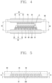
- FIG. 4 is a cross-sectional view illustrating the power module according to FIG. 1 , taken along line “IV-IV”.
- FIG. 5 is an enlarged partial cross-sectional view illustrating an area “A” of FIG. 4 .
- FIG. 6 is a perspective view illustrating a bonding layer according to FIG. 1 .
- FIG. 7 is a perspective view illustrating another implementation of the bonding layer according to FIG. 6 .
- FIG. 8 is a cross-sectional view illustrating the bonding layer according to FIG. 6 , taken along line “VIII-VIII”.
- FIG. 9 is a flowchart illustrating a process of manufacturing a power module in accordance with one implementation of the present disclosure.
- electrical connection may be used when one component is electrically connected to another component or is connected to enable information communication with another component.
- the electrical connection may be achieved by conducting wires, communication cables, or the like.
- upper and lower used in the following description refer to a direction toward a second substrate 40 and a direction toward a first substrate 30 , respectively.
- a power module 1 that converts power supplied from an external power source (not illustrated) into a three-phase voltage is illustrated.
- a power module 1 may include a power element 10 , a spacer 20 , substrates 30 and 40 , bonding layers 50 , 60 , and 70 , an insulation part 80 , and anti-tilting (or tilting prevention) members 100 .
- the power module 1 may include a semiconductor component such as a diode (not illustrated) in addition to the power element 10 .
- the power element 10 may perform a switching operation, which is an operation of converting power supplied from an external power source into power for driving a motor and supplying the converted power.
- a semiconductor device such as an insulated gate bipolar transistor (IGBT) may be used as the power element 10 .
- IGBT insulated gate bipolar transistor
- GTO gate turn-off thyristor
- the power element 10 may include electrodes formed on both surfaces thereof.
- a gate electrode and an emitter electrode may be provided on an upper surface of the power element 10
- a collector electrode may be provided on a lower surface of the power element 10 .
- Each electrode that may be provided on the power element 10 is a well-known technology, and thus a detailed description thereof will be omitted.
- a heat sink for dissipating heat generated from the power element 10 may be provided in the power module 1 .
- the heat sink may be implemented as a heat dissipation plate (not illustrated).
- the power module 1 may have a double-faced (double-sided) cooling structure that dissipates heat to both sides of the power element 10 .
- the substrates 30 and 40 may be provided on upper and lower sides of the power element 10 , and each of the substrates 30 and 40 may be coupled to a heat sink (not illustrated) for dissipating heat transferred from the power element 10 in a contact manner.
- a spacer for securing an insulation distance between the substrates 30 and 40 may be provided.
- the spacer 20 may be connected to the power element 10 in a manner of facing one surface of the power element 10 , and be used to keep the substrates 30 and 40 located on the upper and lower sides of the power element 10 apart.
- an insulation distance between the substrates 30 and 40 may be secured.
- the spacer 20 may have a predetermined height to achieve the insulation distance between the substrates 30 and 40 , and be connected to the power element 10 in a manner that a lower surface thereof faces the upper surface of the power element 10 .
- the spacer 20 may be disposed at a position that corresponds to an electrode formed on the upper surface of the power element 10 .
- the spacer 20 may be connected to the substrate 40 in a manner that an upper surface thereof faces a lower surface of the substrate 40 .
- the spacer 20 may be formed of a material having excellent thermal conductivity and electrical conductivity.
- the spacer 20 may be made of a material such as Al—Si—C or Cu.
- the electrode formed on the upper surface of the power element 10 and a metal portion of the substrate 40 located at the upper side of the power element 10 may be electrically connected to each other through the spacer 20 .
- heat generated from the power element 10 may be transferred to the substrate 40 located at the upper side of the power element 10 through the spacer 20 .
- a heat sink (not illustrated) may be coupled to an upper surface of the substrate 40 in a contact manner, so that heat transferred to the substrate 40 may be dissipated through the heat sink (not illustrated).
- the substrates 30 and 40 may be provided at the upper and lower sides of the power element 10 , respectively.
- the first substrate 30 facing the lower surface of the power element 10 may be disposed at the lower side of the power element 10
- the second substrate 40 facing the upper surface of the spacer 20 may be disposed at the upper side of the power element 10 .
- first substrate 30 and the second substrate 40 may be spaced apart from each other by a predetermined distance with the power element 10 interposed therebetween.
- the first substrate 30 and the second substrate 40 may be implemented as insulating plates each having metal plates on both upper and lower surfaces thereof.
- the first substrate 30 may include a first insulating plate 31 and first metal plates 32 disposed on both upper and lower surfaces of the first insulating plate 31
- the second substrate 40 may include a second insulating plate 41 (see FIG. 4 ) and second metal plates 42 (see FIG. 4 ) disposed on both upper and lower surfaces of the second insulating plate 41 .
- the first insulating plate 31 and the second insulating plate 41 may be made of a material having high thermal conductivity and insulating properties. Accordingly, insulation between the first metal plates 32 , and between the second metal plates 42 may be achieved while smoothly transferring heat generated from the power element 10 .
- the first metal plates 32 and the second metal plates 42 may be electrically connected to the power element 10 and the spacer 20 so as to transmit electrical signals generated from the power element 10 .
- the first metal plate 32 disposed on an upper surface of the first substrate 30 may be electrically connected to an electrode disposed on the lower surface of the power element 10 .
- the first metal plate 32 disposed on the upper surface of the first substrate 30 may be located at a position corresponding to the electrode disposed on the lower surface of the power element 10 .
- the first metal plate 32 disposed on the upper surface of the first substrate 30 may be formed in various shapes according to the arrangement structure of the power element 10 .
- the second metal plate 42 disposed on the lower surface of the second substrate 40 may be electrically connected to the upper surface of the spacer 20 .
- the second metal plate 42 may be located at a position corresponding to the spacer 20 .
- the second metal plate 42 disposed on the lower surface of the second substrate 40 may have various shapes according to the arrangement structure of the spacer 20 .
- the second metal plate 42 disposed on the lower surface of the second substrate 40 may be electrically connected to the electrode disposed on the upper surface of the power element 10 .
- the first substrate 30 and the second substrate 40 may be implemented as direct bonded copper (BDC) substrates.
- BDC direct bonded copper
- the present disclosure is not limited thereto, and may be implemented with various known substrates that can be used in the power module 1 .
- Heat sinks may be coupled to the lower surface of the first substrate 30 and the upper surface of the second substrate 40 , respectively, in the contact manner. Accordingly, heat generated from the power element 10 may be dissipated to the heat sink through the first substrate 30 . In addition, heat generated from the power element 10 may be dissipated to the heat sink through the spacer 20 and the second substrate 40 .
- heat generated from the power element 10 can be dissipated to both upper and lower surfaces of the power element 10 .
- heat dissipation performance of dissipating heat generated in the power element 10 may be improved.
- a bonding layer may be disposed between two members, facing each other, among the power element 10 , the spacer 20 , the first substrate 30 , and the second substrate 40 .
- the two members may be firmly coupled to each other by the bonding layer.
- the bonding layers (first, second, and third bonding layers) 50 , 60 , and 70 may bond (couple) two members facing each other.
- the first bonding layer 50 may be disposed between the upper surface of the power element 10 and the lower surface of the spacer 20 so as to allow the power element 10 and the spacer 20 to be coupled to each other.
- the second bonding layer 60 may be disposed between the lower surface of the power element 10 and the upper surface of the first substrate 30 so as to allow the power element 10 and the first substrate 30 to be coupled to each other.
- the third bonding layer 70 may be disposed between the upper surface of the spacer 20 and the lower surface of the second substrate 40 so as to allow the spacer 20 and the second substrate 40 to be coupled to each other.
- a bonding material having excellent thermal conductivity and electrical conductivity may be used for each of the bonding layers 50 , 60 , and 70 , and each of the bonding layers 50 , 60 , and 70 may be formed by soldering or sintering.
- Such bonding material that forms the bonding layers 50 , 60 , and 70 may include Ag, Cu, Sn—Cu, or the like.
- the insulation part 80 may be disposed between the first substrate 30 and the second substrate 40 .
- the insulation part 80 may prevent insulation breakdown from occurring between the adjacent power elements 10 or between the first and second substrates 30 and 40 .
- the insulation part 80 may be formed by molding an insulating material between the first substrate 30 and the second substrate 40 .
- the power module 1 may include the anti-tilting member 100 in at least one of the bonding layers 50 , 60 , and 70 .
- the bonding layers 50 , 60 , and 70 may be formed through a process of melting a bonding material between two members to be bonded, and solidifying the melted bonding material. As the melted bonding material is solidified, the two members may be bonded to each other.
- a difference may occur between a speed at which a portion of the melted bonding material is solidified and a speed at which another portion is solidified.
- a difference in thickness between arbitrary two portions of the bonding layer may be increased.
- two members that are bonded to each other by the bonding layer may be bonded at a predetermined angle. That is, one of the two members bonded to each other may be inclined with respect to the other member.
- FIG. 3 a power module of the related art in a tilted state caused during the assembly process is illustrated.
- the power module according to FIG. 3 includes a power element 1000 , a spacer 2000 , substrates (first and second substrates) 3000 and 4000 , bonding layers 5000 , 6000 , and 7000 , and an insulation part 8000 .
- FIG. 3 Structures and functions of the components disclosed in FIG. 3 are the same as those of the power element 10 , the spacer 20 , the substrates 30 and 40 , the bonding layers 50 , 60 , and 70 , and the insulation part 80 according to the implementation of the present disclosure, so description thereof will be replaced with the above description.
- the bonding layer 5000 illustrated in FIG. 3 is formed by solidifying a melted bonding material, and a difference may occur between a speed at which a portion of the melted bonding material is solidified and a speed at which another portion is solidified.
- a difference in thickness between arbitrary two portions of the bonding layer may be increased.
- the spacer 2000 and the power element 1000 that are bonded to each other by the bonding layer 5000 may be bonded at a predetermined angle.
- the spacer 2000 that is coupled to the upper side of the power element 1000 may be inclined at a predetermined angle with respect to the power element 1000 .
- a left side of the bonding layer 5000 has a first thickness H 1 and a right side thereof has a second thickness H 2 .
- the second thickness H 2 is greater than the first thickness H 1 .
- a distance between the spacer 2000 and the power element 1000 at the left side of the bonding layer 5000 having the first thickness H 1 may be less than a distance between the spacer 2000 and the power element 1000 at the right side of the bonding layer 5000 .
- stress which is higher than a stress value designed to be withstood or endured by the power element 1000 , may be applied, causing damage to the power element 1000 .
- the spacer 2000 that is coupled to the upper side of the bonding layer 5000 may be coupled in a manner of being tilted from right to left.
- the second substrate 4000 that is coupled to the spacer 2000 is also assembled in a tilted state.
- the second substrate 4000 is assembled in the tilted state with respect to the first substrate 3000 .
- the insulation part 8000 is disposed between the first substrate 3000 and the second substrate 4000 that are coupled to each other.
- the insulation part 8000 is formed by fixing the first and second substrates 3000 and 4000 coupled to each other on a mold having a specific or predetermined shape, and then injecting an insulating material into the mold.
- the insulation part 8000 may be formed by a molding method.
- excessive stress may be applied to a specific portion of the power element 1000 by the mold.
- excessive stress may be applied to a specific portion of the power element 1000 . This may cause damage to the power element 1000 .
- Tilting caused by the difference in thickness of the bonding layer 5000 may also occur in the other bonding layers 6000 and 7000 .
- tilting may occur when the first substrate 3000 and the power element 1000 are coupled to each other, and tilting may occur when the second substrate 4000 and the spacer 2000 are coupled to each other.
- Heat sinks (not illustrated) that dissipate heat generated in the power element 1000 may be coupled to the lower surface of the first substrate 3000 and an upper surface of the second substrate 4000 , respectively, in the contact manner.
- first substrate 3000 and the second substrate 4000 are assembled in a tilted state, a separation between the heat sink (not illustrated) and the first substrate 3000 and/or the heat sink (not illustrated) and the second substrate 4000 may occur.
- an amount of heat transferred to the heat sinks (not illustrated) from the first substrate 3000 and the second substrate 4000 per unit hour may be reduced.
- heat dissipation performance of the power element 1000 may be reduced.
- the power module 1 may include an anti-tilting member 100 in at least one of the first bonding layer 50 , the second bonding layer 60 , and the third bonding layer 70 .
- the anti-tilting member 100 may be provided in plurality, each having a predetermined height in an up-and-down direction.
- the predetermined height may be designed in consideration of a thickness of each of the bonding layers 50 , 60 , and 70 in the up-and-down direction. That is, the anti-tilting member 100 may have a height equal to a design thickness of the bonding layers 50 , 60 , and 70 .
- the anti-tilting member 100 may have a spherical shape.
- the plurality of anti-tilting members 100 may be disposed between two members to be bonded in a state of being contained in a melted bonding material.
- the bonding material is solidified to form the bonding layer 50 , 60 , 70 containing the anti-tilting members 100
- the anti-tilting members 100 may support the two members together with the bonding layer 50 , 60 , 70 .
- the first bonding layer 50 may include the plurality of anti-tilting members 100 , and the anti-tilting members 100 may support the power element 10 and the spacer 20 together with the first bonding layer 50 between the power element 10 and the spacer 20 .
- the anti-tilting member 100 may be made of a material that does not melt at a temperature at which the bonding material forming the bonding layer 50 , 60 , 70 is melted.
- the anti-tilting members 100 may be disposed by being included in the melted bonding material without being melted.
- the anti-tilting member 100 may be formed of a material that does not react with the bonding material while being included in the melted bonding material. If the anti-tilting member 100 is made of a material having too high reactivity, the anti-tilting member 100 may react with the bonding material and the shape of the anti-tilting member 100 may be melted.
- a height difference may occur between the plurality of anti-tilting members 100 , and thus tilting may occur between the power element 10 and the spacer 20 .
- the anti-tilting member 100 may be made of a material that has a higher melting point than the bonding material and does not react with the melted bonding material.
- the two members bonded may be supported by the anti-tilting members 100 .
- the spacer 20 and the power element 10 may be supported by the plurality of anti-tilting members 100 interposed therebetween.
- the spacer 20 and the power element 10 may be supported by the plurality of anti-tilting members 100 interposed therebetween.
- the spacer 20 and the power element 10 can be prevented from being coupled to each other in a tilted state.
- the second bonding layer 60 may also include the plurality of anti-tilting members 100 so as to suppress the occurrence of tilting. More specifically, it can be suppressed that the first substrate 30 and the power element 10 are coupled to each other in a tilted state.
- the third bonding layer 70 may also include the plurality of anti-tilting members 100 so as to suppress the occurrence of tilting. More specifically, it can be suppressed that the second substrate 40 and the spacer 20 are coupled to each other in a tilted state.
- the bonding layers 50 , 60 , and 70 may be made of a material including copper (Cu).
- the bonding layers 50 , 60 , and 70 may be made of a tin-copper alloy (Sn—Cu).
- the anti-tilting member 100 may be made of a nickel (Ni) material.
- the thickness of the bonding layers 50 , 60 , and 70 in the up-and-down direction may be within a predetermined error range.
- the thickness of the bonding layers 50 , 60 , and 70 in the up-and-down direction may be within an error range of 7 ⁇ m.
- a difference between the highest portion and the lowest portion of the bonding layers 50 , 60 , and 70 in the up-and-down direction (height direction) may be 20 ⁇ m or less.
- a left side of the first bonding layer 50 may have a first thickness H 1 and a right side thereof may have a second thickness H 2 .
- a difference between the second thickness H 2 and the first thickness H 1 may be a predetermined value or less, thereby improving reliability of the power module 1 .
- the difference between the second thickness H 2 and the first thickness H 1 may be 7 ⁇ m or less, thereby improving the reliability of the power module 1 .
- the second and third bonding layers 60 and 70 may be formed such that the error in thickness is included within the predetermined error range.
- a difference between the thickest portion and the thinnest portion of the bonding layers 60 and 70 may be 7 ⁇ m or less.
- a difference between the shortest distance between the first substrate 30 and the second substrate 40 at one end of the first substrate 30 and the shortest distance between the first substrate 30 and the second substrate 40 at another end of the first substrate 30 may be less than or equal to a predetermined value.
- the predetermined value may be less than or equal to 20 ⁇ m.
- the difference between the shortest distance D 1 between the first substrate 30 and the second substrate 40 at the left end of the first substrate 30 and the shortest distance D 2 between the first substrate 30 and the second substrate 40 at the right end of the first substrate 30 may be 20 ⁇ m or less.
- the difference between the shortest distance between the first substrate 30 and the second substrate 40 at the one end of the first substrate 30 and the shortest distance between the first substrate 30 and the second substrate 40 at the another end of the first substrate 30 is excessively increased, the excessive increase in thermal stress and the deterioration in heat dissipation performance may occur.
- the problems such as the excessive increase in thermal stress and the deterioration in heat dissipation performance may occur.
- the difference between the shortest distance D 1 between the first substrate 30 and the second substrate 40 at the left end of the first substrate 30 and the shortest distance between the first substrate 30 and the second substrate 40 at the right end of the first substrate 30 is reduced to a predetermined value or less (preferably, 20 ⁇ m), the problems such as the excessive increase in thermal stress and the deterioration of the heat dissipation performance can be suppressed.
- the first substrate 30 and the second substrate 40 may form a predetermined angle that is extremely small.
- the first substrate 30 and the second substrate 40 may be coupled substantially in parallel to each other.
- the plurality of anti-tilting members 100 may be evenly disposed in the entire first bonding layer 50 .
- the first bonding layer 50 may have a rectangular cross section, and some of the plurality of anti-tilting members 100 may be disposed at vertexes of the rectangle, respectively. Accordingly, when the spacer 20 and the power module 10 are coupled to each other, the spacer 20 may be prevented from being tilted with respect to the power module 10 .
- the first bonding layer 50 may have a polygonal cross section, and some of the plurality of anti-tilting members 100 may be disposed at vertexes of the polygon, respectively.
- some of the plurality of anti-tilting members 100 may be disposed on a periphery of the first bonding layer 50 . Accordingly, when the spacer 20 and the power element 10 are coupled to each other, the spacer 20 may be prevented from tilted with respect to the power element 10 .
- a plurality of anti-tilting members 100 included in the second bonding layer 60 and the third bonding layer 70 may also be disposed like the plurality of anti-tilting members 100 included in the first bonding layer 60 .
- the anti-tilting member 100 may have a spherical shape.
- the present disclosure is not limited thereto, and the ant-tilting member 100 may alternatively be formed in a polygonal column shape having a predetermined height in an up-and-down direction.
- the anti-tilting member 100 may have a cylindrical shape.
- a mixing ratio of the bonding layer 50 , 60 , 70 and the plurality of anti-tilting members 100 may preferably be designed.
- the bonding performance of the bonding layer 50 , 60 , 70 may be reduced, which may cause reliability of the power module 1 to be lowered.
- the anti-tilting members 100 may preferably be included in the bonding layer 50 , 60 , 70 by an amount that is large enough to allow the assembly error of the power module 1 to be within the designed error range and to suppress the bonding performance of the bonding layers 50 , 60 , and 70 from being excessively deteriorated.
- a cross-sectional area of the first bonding layer 50 may be defined as a first area A 1
- the sum of cross-sectional areas of the plurality of anti-tilting members 100 may be defined as a second area A 2 .
- the second area A 2 may be in the range of 20% to 25% of the first area A 1 .
- the bonding performance of the first bonding layer 50 may not be excessively deteriorated, and the assembly error of the power module 1 may be within the designed error range.
- FIG. 9 a flowchart of a process of manufacturing the power module 1 according to an implementation of the present disclosure is shown.
- a bonding material may be melted and applied to one surface of the first substrate 30 .
- the bonding material may be a material having excellent thermal conductivity and electrical conductivity.
- the bonding material may be soldered to positions corresponding to components to be mounted on the one surface of the first substrate 30 .
- the melted bonding material may contain the plurality of anti-tilting members 100 .
- the power element 10 , diodes (not illustrated), lead frames (not illustrated), and the like may be mounted on the one surface of the first substrate 30 .
- the one surface of the first substrate 30 to which the melted bonding material has been applied may face the second substrate 40 that is disposed to be spaced apart from the first substrate 30 by a predetermined distance.
- the power element 10 may be placed on the melted and applied bonding material.
- the power element 10 may be pressed with predetermined pressure toward the one surface of the first substrate 30 .
- the predetermined pressure may be pressure designed for the bonding between the power element 10 and the first substrate 30 .
- the melted bonding material may be solidified. Accordingly, the power element 10 and the first substrate 30 may be bonded to each other.
- the power element 10 and the first substrate 30 are supported by the plurality of anti-tilting members 100 interposed therebetween, the power element 10 may be prevented from being mounted in a tilted state with respect to the first substrate 30 .
- the diodes (not illustrated) and the lead frames (not illustrated) may also be mounted on the one surface of the first substrate 30 in the same manner.
- the power element 10 mounted on the one surface of the first substrate 30 may be electrically connected to the first substrate 30 .
- the bonding material may be a material having excellent thermal conductivity and electrical conductivity.
- the bonding material may be soldered to a position corresponding to the spacer 20 to be mounted on the one surface of the second substrate 40 .
- the melted bonding material may contain the plurality of anti-tilting members 100 .
- the spacer 20 may be placed on the melted and applied bonding material.
- the spacer 20 may be pressed with predetermined pressure toward the one surface of the second substrate 40 .
- the predetermined pressure may be pressure designed for the bonding between the spacer 20 and the second substrate 40 .
- the spacer 20 and the second substrate 40 face each other, the melted bonding material may be solidified. Accordingly, the spacer 20 and the second substrate 40 may be bonded to each other.
- the spacer 20 and the second substrate 40 are supported by the plurality of anti-tilting members 100 interposed therebetween, the spacer 20 may be prevented from being mounted in a tilted state with respect to the second substrate 40 .
- the spacer 20 mounted on the one surface of the second substrate 40 may be electrically connected to the second substrate 40 .
- the power element 10 may be bonded to the one surface of the first substrate 30
- the spacer 20 may be bonded to the one surface of the second substrate 40 .
- a bonding material may be melted and applied to one surface of the power element 10 .
- the bonding material may be a material having excellent thermal conductivity and electrical conductivity.
- the one surface of the power element 10 may be defined as a surface opposite to a surface that the power element 10 faces the first substrate 30 .
- the melted bonding material may contain the plurality of anti-tilting members 100 .
- Another surface of the spacer 20 mounded on the second substrate 40 may be placed on the melted and applied bonding material.
- the spacer 20 and the second substrate 40 may be pressed with predetermined pressure toward the one surface of the power element 10 .
- the predetermined pressure may be pressure designed for the bonding between the spacer 20 and the power element 10 .
- the melted bonding material may be solidified.
- the spacer 20 and the power element 10 may be bonded to each other.
- the first substrate 30 , the power element 10 , the spacer 20 , and the second substrate 40 are sequentially arranged to be assembled.
- the spacer 20 and the power element 10 are supported by the plurality of anti-tilting members 100 interposed therebetween, the spacer 20 may be prevented from being mounted in a tilted state with respect to the power element 10 .
- an insulating material may be molded between the first substrate 30 and the second substrate 40 .
- the insulating material may be applied between the first and second substrates 30 and 40 so as to form the insulation part 80 .
- insulation internal pressure of the power element 10 may be secured.
- the power element 10 since the power element 10 is not exposed to outside, the power element 10 can be protected from the outside.
- Heat sinks may be coupled to another surface of the first substrate 30 and another surface of the second substrate 40 , respectively.
- the another surface of the first substrate 30 may be defined as a surface opposite to the one surface of the first substrate 30
- the another surface of the second substrate 40 may be defined as a surface opposite to the one surface of the second substrate 40 .
- Heat generated in the power element 10 may be dissipated through the spacer 20 , the second substrate 40 , and the heat sink.
- heat generated in the power element 10 may be dissipated through the first substrate 30 and the heat sink.
- heat generated from the power element 10 may be dissipated to the both surfaces of the power element 10 .
- the heat generated in the power element 10 can be effectively dissipated.
- heat transfer efficiency can be improved between the first and second substrates 30 and 40 and the heat sinks.
- the heat generated in the power element 10 can be effectively dissipated, and the damage to the power element 10 due to the excessive increase in the internal temperature of the power module 1 can be suppressed.
Landscapes
- Engineering & Computer Science (AREA)
- Microelectronics & Electronic Packaging (AREA)
- Power Engineering (AREA)
- Computer Hardware Design (AREA)
- Physics & Mathematics (AREA)
- Condensed Matter Physics & Semiconductors (AREA)
- General Physics & Mathematics (AREA)
- Chemical & Material Sciences (AREA)
- Materials Engineering (AREA)
- Ceramic Engineering (AREA)
- Thermal Sciences (AREA)
- Manufacturing & Machinery (AREA)
- Cooling Or The Like Of Semiconductors Or Solid State Devices (AREA)
Abstract
Description
- Korean Registration Patent Publication No. 10-1786343 (Oct. 18, 2017)
Claims (20)
Applications Claiming Priority (2)
| Application Number | Priority Date | Filing Date | Title |
|---|---|---|---|
| KR1020200036951A KR20210120355A (en) | 2020-03-26 | 2020-03-26 | Power module of double-faced cooling |
| KR10-2020-0036951 | 2020-03-26 |
Publications (2)
| Publication Number | Publication Date |
|---|---|
| US20210305193A1 US20210305193A1 (en) | 2021-09-30 |
| US11735557B2 true US11735557B2 (en) | 2023-08-22 |
Family
ID=75202958
Family Applications (1)
| Application Number | Title | Priority Date | Filing Date |
|---|---|---|---|
| US17/207,086 Active 2041-09-30 US11735557B2 (en) | 2020-03-26 | 2021-03-19 | Power module of double-faced cooling |
Country Status (3)
| Country | Link |
|---|---|
| US (1) | US11735557B2 (en) |
| EP (1) | EP3890009A1 (en) |
| KR (1) | KR20210120355A (en) |
Families Citing this family (1)
| Publication number | Priority date | Publication date | Assignee | Title |
|---|---|---|---|---|
| JP2022029328A (en) * | 2020-08-04 | 2022-02-17 | パナソニックIpマネジメント株式会社 | Semiconductor device and manufacturing method thereof |
Citations (21)
| Publication number | Priority date | Publication date | Assignee | Title |
|---|---|---|---|---|
| US20120020028A1 (en) * | 2010-07-20 | 2012-01-26 | Lsi Corporation | Stacked interconnect heat sink |
| US20140167263A1 (en) * | 2012-12-13 | 2014-06-19 | Taiwan Semiconductor Manufacturing Company, Ltd. | Methods and Apparatus for Package with Interposers |
| US20140291830A1 (en) * | 2013-04-01 | 2014-10-02 | Taejoo Hwang | Semiconductor packages having package-on-package structures |
| US20150155243A1 (en) * | 2013-12-04 | 2015-06-04 | Taiwan Semiconductor Manufacturing Company, Ltd. | Warpage Control in Package-on-Package Structures |
| US20150162265A1 (en) * | 2013-12-06 | 2015-06-11 | Cha-Jea JO | Semiconductor package and method of manufacturing the same |
| US20160113107A1 (en) * | 2014-10-15 | 2016-04-21 | Delta Electronics, Inc. | Power module |
| US20160126204A1 (en) * | 2014-10-30 | 2016-05-05 | Toyota Jidosha Kabushiki Kaisha | Semiconductor device and method of manufacturing semiconductor device |
| US20160148820A1 (en) * | 2014-08-29 | 2016-05-26 | Taiwan Semiconductor Manufacturing Company, Ltd. | Package-on-package structures and methods of manufacture thereof |
| JP2016146450A (en) | 2015-02-09 | 2016-08-12 | 株式会社デンソー | Electronic apparatus |
| US20160255714A1 (en) | 2015-02-26 | 2016-09-01 | Denso Corporation | Power converter |
| US20170154878A1 (en) * | 2015-11-26 | 2017-06-01 | Jae-choon Kim | Stack package and method of manufacturing the stack package |
| KR101786343B1 (en) | 2016-05-04 | 2017-10-18 | 현대자동차주식회사 | Power module of double-faced cooling |
| US20190214358A1 (en) * | 2018-01-11 | 2019-07-11 | Samsung Electronics Co., Ltd. | Semiconductor device, semiconductor package including semiconductor device, and method of manufacturing semiconductor device |
| US20200006214A1 (en) * | 2018-06-29 | 2020-01-02 | Taiwan Semiconductor Manufacturing Company, Ltd. | Fan-out Package with Controllable Standoff |
| US20200212006A1 (en) * | 2018-12-28 | 2020-07-02 | Taiwan Semiconductor Manufacturing Co., Ltd. | Package contact structure, semiconductor package and manufacturing method thereof |
| US20200212018A1 (en) * | 2018-12-26 | 2020-07-02 | Taiwan Semiconductor Manufacturing Company, Ltd. | Integrated Circuit Package and Method |
| US20200219786A1 (en) * | 2019-01-08 | 2020-07-09 | Taiwan Semiconductor Manufacturing Company, Ltd. | Package Structure and Method and Equipment for Forming the Same |
| US20200227380A1 (en) * | 2019-01-11 | 2020-07-16 | Toyota Jidosha Kabushiki Kaisha | Semiconductor device and manufacturing method thereof |
| US20210050300A1 (en) * | 2019-07-02 | 2021-02-18 | iCometrue Company Ltd. | Logic drive based on multichip package comprising standard commodity fpga ic chip with cooperating or supporting circuits |
| US20210118770A1 (en) * | 2019-10-18 | 2021-04-22 | Taiwan Semiconductor Manufacturing Company, Ltd. | Thermal interface materials, 3d semiconductor packages and methods of manufacture |
| US20210257275A1 (en) * | 2020-02-13 | 2021-08-19 | Samsung Electronics Co., Ltd. | Semiconductor package |
-
2020
- 2020-03-26 KR KR1020200036951A patent/KR20210120355A/en unknown
-
2021
- 2021-03-19 US US17/207,086 patent/US11735557B2/en active Active
- 2021-03-23 EP EP21164205.3A patent/EP3890009A1/en active Pending
Patent Citations (21)
| Publication number | Priority date | Publication date | Assignee | Title |
|---|---|---|---|---|
| US20120020028A1 (en) * | 2010-07-20 | 2012-01-26 | Lsi Corporation | Stacked interconnect heat sink |
| US20140167263A1 (en) * | 2012-12-13 | 2014-06-19 | Taiwan Semiconductor Manufacturing Company, Ltd. | Methods and Apparatus for Package with Interposers |
| US20140291830A1 (en) * | 2013-04-01 | 2014-10-02 | Taejoo Hwang | Semiconductor packages having package-on-package structures |
| US20150155243A1 (en) * | 2013-12-04 | 2015-06-04 | Taiwan Semiconductor Manufacturing Company, Ltd. | Warpage Control in Package-on-Package Structures |
| US20150162265A1 (en) * | 2013-12-06 | 2015-06-11 | Cha-Jea JO | Semiconductor package and method of manufacturing the same |
| US20160148820A1 (en) * | 2014-08-29 | 2016-05-26 | Taiwan Semiconductor Manufacturing Company, Ltd. | Package-on-package structures and methods of manufacture thereof |
| US20160113107A1 (en) * | 2014-10-15 | 2016-04-21 | Delta Electronics, Inc. | Power module |
| US20160126204A1 (en) * | 2014-10-30 | 2016-05-05 | Toyota Jidosha Kabushiki Kaisha | Semiconductor device and method of manufacturing semiconductor device |
| JP2016146450A (en) | 2015-02-09 | 2016-08-12 | 株式会社デンソー | Electronic apparatus |
| US20160255714A1 (en) | 2015-02-26 | 2016-09-01 | Denso Corporation | Power converter |
| US20170154878A1 (en) * | 2015-11-26 | 2017-06-01 | Jae-choon Kim | Stack package and method of manufacturing the stack package |
| KR101786343B1 (en) | 2016-05-04 | 2017-10-18 | 현대자동차주식회사 | Power module of double-faced cooling |
| US20190214358A1 (en) * | 2018-01-11 | 2019-07-11 | Samsung Electronics Co., Ltd. | Semiconductor device, semiconductor package including semiconductor device, and method of manufacturing semiconductor device |
| US20200006214A1 (en) * | 2018-06-29 | 2020-01-02 | Taiwan Semiconductor Manufacturing Company, Ltd. | Fan-out Package with Controllable Standoff |
| US20200212018A1 (en) * | 2018-12-26 | 2020-07-02 | Taiwan Semiconductor Manufacturing Company, Ltd. | Integrated Circuit Package and Method |
| US20200212006A1 (en) * | 2018-12-28 | 2020-07-02 | Taiwan Semiconductor Manufacturing Co., Ltd. | Package contact structure, semiconductor package and manufacturing method thereof |
| US20200219786A1 (en) * | 2019-01-08 | 2020-07-09 | Taiwan Semiconductor Manufacturing Company, Ltd. | Package Structure and Method and Equipment for Forming the Same |
| US20200227380A1 (en) * | 2019-01-11 | 2020-07-16 | Toyota Jidosha Kabushiki Kaisha | Semiconductor device and manufacturing method thereof |
| US20210050300A1 (en) * | 2019-07-02 | 2021-02-18 | iCometrue Company Ltd. | Logic drive based on multichip package comprising standard commodity fpga ic chip with cooperating or supporting circuits |
| US20210118770A1 (en) * | 2019-10-18 | 2021-04-22 | Taiwan Semiconductor Manufacturing Company, Ltd. | Thermal interface materials, 3d semiconductor packages and methods of manufacture |
| US20210257275A1 (en) * | 2020-02-13 | 2021-08-19 | Samsung Electronics Co., Ltd. | Semiconductor package |
Also Published As
| Publication number | Publication date |
|---|---|
| KR20210120355A (en) | 2021-10-07 |
| EP3890009A1 (en) | 2021-10-06 |
| US20210305193A1 (en) | 2021-09-30 |
Similar Documents
| Publication | Publication Date | Title |
|---|---|---|
| JP7204770B2 (en) | Double-sided cooling power module and manufacturing method thereof | |
| US7772709B2 (en) | Resin sealed semiconductor device and manufacturing method therefor | |
| US7015578B2 (en) | Semiconductor unit with cooling system | |
| JP6257478B2 (en) | Power semiconductor device | |
| CN108735692B (en) | Semiconductor device with a semiconductor device having a plurality of semiconductor chips | |
| US8610263B2 (en) | Semiconductor device module | |
| JP2000164800A (en) | Semiconductor module | |
| US9437508B2 (en) | Method for manufacturing semiconductor device and semiconductor device | |
| JP2007305702A (en) | Semiconductor device and its manufacturing method | |
| CN113039636A (en) | Power semiconductor device | |
| JP2019125708A (en) | Semiconductor device | |
| CN111276447B (en) | Double-sided cooling power module and manufacturing method thereof | |
| US11735557B2 (en) | Power module of double-faced cooling | |
| JP5899952B2 (en) | Semiconductor module | |
| US11201099B2 (en) | Semiconductor device and method of manufacturing the same | |
| JP2012209470A (en) | Semiconductor device, semiconductor device module, and manufacturing method of the semiconductor device | |
| JP2006190728A (en) | Electric power semiconductor device | |
| JP7118205B1 (en) | Semiconductor device and semiconductor module using the same | |
| US10903138B2 (en) | Semiconductor device and method of manufacturing the same | |
| JP7290420B2 (en) | power semiconductor equipment | |
| EP3907756A1 (en) | Power module of double-faced cooling and manufacturing method thereof | |
| JP3644161B2 (en) | Power semiconductor module | |
| JP2020141023A (en) | Semiconductor device | |
| US20240096727A1 (en) | Power Semiconductor Device | |
| WO2023017570A1 (en) | Semiconductor device and inverter unit |
Legal Events
| Date | Code | Title | Description |
|---|---|---|---|
| AS | Assignment |
Owner name: LG ELECTRONICS INC., KOREA, REPUBLIC OF Free format text: ASSIGNMENT OF ASSIGNORS INTEREST;ASSIGNORS:CHOI, SIHO;CHO, SEONGMOO;KIM, KWANGSOO;AND OTHERS;REEL/FRAME:055654/0792 Effective date: 20210318 |
|
| FEPP | Fee payment procedure |
Free format text: ENTITY STATUS SET TO UNDISCOUNTED (ORIGINAL EVENT CODE: BIG.); ENTITY STATUS OF PATENT OWNER: LARGE ENTITY |
|
| STPP | Information on status: patent application and granting procedure in general |
Free format text: DOCKETED NEW CASE - READY FOR EXAMINATION |
|
| AS | Assignment |
Owner name: LG MAGNA E-POWERTRAIN CO., LTD., KOREA, REPUBLIC OF Free format text: ASSIGNMENT OF ASSIGNORS INTEREST;ASSIGNOR:LG ELECTRONICS INC.;REEL/FRAME:057342/0582 Effective date: 20210726 |
|
| STPP | Information on status: patent application and granting procedure in general |
Free format text: NON FINAL ACTION MAILED |
|
| STPP | Information on status: patent application and granting procedure in general |
Free format text: PUBLICATIONS -- ISSUE FEE PAYMENT VERIFIED |
|
| STCF | Information on status: patent grant |
Free format text: PATENTED CASE |