US11656994B2 - Non-volatile memory with optimized read - Google Patents
Non-volatile memory with optimized read Download PDFInfo
- Publication number
- US11656994B2 US11656994B2 US17/306,073 US202117306073A US11656994B2 US 11656994 B2 US11656994 B2 US 11656994B2 US 202117306073 A US202117306073 A US 202117306073A US 11656994 B2 US11656994 B2 US 11656994B2
- Authority
- US
- United States
- Prior art keywords
- data
- cache
- cache segment
- host
- pmr
- Prior art date
- Legal status (The legal status is an assumption and is not a legal conclusion. Google has not performed a legal analysis and makes no representation as to the accuracy of the status listed.)
- Active, expires
Links
- 230000015654 memory Effects 0.000 title claims abstract description 352
- 230000002085 persistent effect Effects 0.000 claims abstract description 18
- 238000000034 method Methods 0.000 claims description 69
- 230000004044 response Effects 0.000 claims description 57
- 230000002093 peripheral effect Effects 0.000 claims description 16
- 230000004931 aggregating effect Effects 0.000 claims description 2
- 230000008901 benefit Effects 0.000 abstract description 9
- 102100027364 Cysteine-rich protein 3 Human genes 0.000 description 161
- 230000008569 process Effects 0.000 description 50
- 238000005516 engineering process Methods 0.000 description 22
- 238000010586 diagram Methods 0.000 description 16
- 238000004891 communication Methods 0.000 description 14
- 238000013519 translation Methods 0.000 description 9
- 238000003491 array Methods 0.000 description 7
- 239000000872 buffer Substances 0.000 description 6
- 238000012546 transfer Methods 0.000 description 6
- 238000012545 processing Methods 0.000 description 5
- 101000626112 Homo sapiens Telomerase protein component 1 Proteins 0.000 description 4
- 102100024553 Telomerase protein component 1 Human genes 0.000 description 4
- 230000008859 change Effects 0.000 description 4
- 239000004065 semiconductor Substances 0.000 description 4
- 230000000712 assembly Effects 0.000 description 3
- 238000000429 assembly Methods 0.000 description 3
- 238000012937 correction Methods 0.000 description 3
- 238000013461 design Methods 0.000 description 3
- 230000006870 function Effects 0.000 description 3
- 238000012005 ligant binding assay Methods 0.000 description 3
- 239000000758 substrate Substances 0.000 description 3
- 102100038815 Nocturnin Human genes 0.000 description 2
- 230000001427 coherent effect Effects 0.000 description 2
- 230000001934 delay Effects 0.000 description 2
- 230000001419 dependent effect Effects 0.000 description 2
- 150000002500 ions Chemical class 0.000 description 2
- 230000005291 magnetic effect Effects 0.000 description 2
- 230000005415 magnetization Effects 0.000 description 2
- 230000007246 mechanism Effects 0.000 description 2
- 229910052751 metal Inorganic materials 0.000 description 2
- 239000002184 metal Substances 0.000 description 2
- 238000012986 modification Methods 0.000 description 2
- 230000004048 modification Effects 0.000 description 2
- 239000007787 solid Substances 0.000 description 2
- 239000007784 solid electrolyte Substances 0.000 description 2
- RYGMFSIKBFXOCR-UHFFFAOYSA-N Copper Chemical compound [Cu] RYGMFSIKBFXOCR-UHFFFAOYSA-N 0.000 description 1
- 101000772194 Homo sapiens Transthyretin Proteins 0.000 description 1
- 101100247669 Quaranfil virus (isolate QrfV/Tick/Afghanistan/EG_T_377/1968) PB1 gene Proteins 0.000 description 1
- 229910017629 Sb2Te3 Inorganic materials 0.000 description 1
- 101150025928 Segment-1 gene Proteins 0.000 description 1
- XUIMIQQOPSSXEZ-UHFFFAOYSA-N Silicon Chemical compound [Si] XUIMIQQOPSSXEZ-UHFFFAOYSA-N 0.000 description 1
- 101100242902 Thogoto virus (isolate SiAr 126) Segment 1 gene Proteins 0.000 description 1
- 102100029290 Transthyretin Human genes 0.000 description 1
- 230000006399 behavior Effects 0.000 description 1
- 230000005540 biological transmission Effects 0.000 description 1
- 230000000903 blocking effect Effects 0.000 description 1
- 230000001413 cellular effect Effects 0.000 description 1
- 239000005387 chalcogenide glass Substances 0.000 description 1
- 238000010276 construction Methods 0.000 description 1
- 229910052802 copper Inorganic materials 0.000 description 1
- 239000010949 copper Substances 0.000 description 1
- 239000004744 fabric Substances 0.000 description 1
- 230000005294 ferromagnetic effect Effects 0.000 description 1
- 238000007667 floating Methods 0.000 description 1
- GNPVGFCGXDBREM-UHFFFAOYSA-N germanium atom Chemical group [Ge] GNPVGFCGXDBREM-UHFFFAOYSA-N 0.000 description 1
- 230000006872 improvement Effects 0.000 description 1
- 239000012212 insulator Substances 0.000 description 1
- 239000012464 large buffer Substances 0.000 description 1
- 238000004519 manufacturing process Methods 0.000 description 1
- 239000000463 material Substances 0.000 description 1
- 238000001465 metallisation Methods 0.000 description 1
- 239000000203 mixture Substances 0.000 description 1
- 230000006855 networking Effects 0.000 description 1
- 230000009467 reduction Effects 0.000 description 1
- 230000001105 regulatory effect Effects 0.000 description 1
- 230000000717 retained effect Effects 0.000 description 1
- 230000002441 reversible effect Effects 0.000 description 1
- 229910052710 silicon Inorganic materials 0.000 description 1
- 239000010703 silicon Substances 0.000 description 1
- 229910052709 silver Inorganic materials 0.000 description 1
- 239000004332 silver Substances 0.000 description 1
- 230000001360 synchronised effect Effects 0.000 description 1
- 239000010409 thin film Substances 0.000 description 1
- 230000009466 transformation Effects 0.000 description 1
- WFKWXMTUELFFGS-UHFFFAOYSA-N tungsten Chemical compound [W] WFKWXMTUELFFGS-UHFFFAOYSA-N 0.000 description 1
- 229910052721 tungsten Inorganic materials 0.000 description 1
- 239000010937 tungsten Substances 0.000 description 1
Images


Classifications
-
- G—PHYSICS
- G06—COMPUTING; CALCULATING OR COUNTING
- G06F—ELECTRIC DIGITAL DATA PROCESSING
- G06F12/00—Accessing, addressing or allocating within memory systems or architectures
- G06F12/02—Addressing or allocation; Relocation
- G06F12/08—Addressing or allocation; Relocation in hierarchically structured memory systems, e.g. virtual memory systems
- G06F12/0802—Addressing of a memory level in which the access to the desired data or data block requires associative addressing means, e.g. caches
- G06F12/0866—Addressing of a memory level in which the access to the desired data or data block requires associative addressing means, e.g. caches for peripheral storage systems, e.g. disk cache
- G06F12/0868—Data transfer between cache memory and other subsystems, e.g. storage devices or host systems
-
- G—PHYSICS
- G06—COMPUTING; CALCULATING OR COUNTING
- G06F—ELECTRIC DIGITAL DATA PROCESSING
- G06F3/00—Input arrangements for transferring data to be processed into a form capable of being handled by the computer; Output arrangements for transferring data from processing unit to output unit, e.g. interface arrangements
- G06F3/06—Digital input from, or digital output to, record carriers, e.g. RAID, emulated record carriers or networked record carriers
- G06F3/0601—Interfaces specially adapted for storage systems
- G06F3/0602—Interfaces specially adapted for storage systems specifically adapted to achieve a particular effect
- G06F3/061—Improving I/O performance
- G06F3/0611—Improving I/O performance in relation to response time
-
- G—PHYSICS
- G11—INFORMATION STORAGE
- G11C—STATIC STORES
- G11C16/00—Erasable programmable read-only memories
- G11C16/02—Erasable programmable read-only memories electrically programmable
- G11C16/04—Erasable programmable read-only memories electrically programmable using variable threshold transistors, e.g. FAMOS
- G11C16/0483—Erasable programmable read-only memories electrically programmable using variable threshold transistors, e.g. FAMOS comprising cells having several storage transistors connected in series
-
- G—PHYSICS
- G06—COMPUTING; CALCULATING OR COUNTING
- G06F—ELECTRIC DIGITAL DATA PROCESSING
- G06F12/00—Accessing, addressing or allocating within memory systems or architectures
- G06F12/02—Addressing or allocation; Relocation
- G06F12/08—Addressing or allocation; Relocation in hierarchically structured memory systems, e.g. virtual memory systems
- G06F12/0802—Addressing of a memory level in which the access to the desired data or data block requires associative addressing means, e.g. caches
- G06F12/0866—Addressing of a memory level in which the access to the desired data or data block requires associative addressing means, e.g. caches for peripheral storage systems, e.g. disk cache
- G06F12/0871—Allocation or management of cache space
-
- G—PHYSICS
- G06—COMPUTING; CALCULATING OR COUNTING
- G06F—ELECTRIC DIGITAL DATA PROCESSING
- G06F12/00—Accessing, addressing or allocating within memory systems or architectures
- G06F12/02—Addressing or allocation; Relocation
- G06F12/08—Addressing or allocation; Relocation in hierarchically structured memory systems, e.g. virtual memory systems
- G06F12/0802—Addressing of a memory level in which the access to the desired data or data block requires associative addressing means, e.g. caches
- G06F12/0877—Cache access modes
- G06F12/0884—Parallel mode, e.g. in parallel with main memory or CPU
-
- G—PHYSICS
- G06—COMPUTING; CALCULATING OR COUNTING
- G06F—ELECTRIC DIGITAL DATA PROCESSING
- G06F13/00—Interconnection of, or transfer of information or other signals between, memories, input/output devices or central processing units
- G06F13/14—Handling requests for interconnection or transfer
- G06F13/16—Handling requests for interconnection or transfer for access to memory bus
- G06F13/1668—Details of memory controller
-
- G—PHYSICS
- G06—COMPUTING; CALCULATING OR COUNTING
- G06F—ELECTRIC DIGITAL DATA PROCESSING
- G06F13/00—Interconnection of, or transfer of information or other signals between, memories, input/output devices or central processing units
- G06F13/38—Information transfer, e.g. on bus
- G06F13/42—Bus transfer protocol, e.g. handshake; Synchronisation
- G06F13/4204—Bus transfer protocol, e.g. handshake; Synchronisation on a parallel bus
- G06F13/4221—Bus transfer protocol, e.g. handshake; Synchronisation on a parallel bus being an input/output bus, e.g. ISA bus, EISA bus, PCI bus, SCSI bus
-
- G—PHYSICS
- G06—COMPUTING; CALCULATING OR COUNTING
- G06F—ELECTRIC DIGITAL DATA PROCESSING
- G06F13/00—Interconnection of, or transfer of information or other signals between, memories, input/output devices or central processing units
- G06F13/38—Information transfer, e.g. on bus
- G06F13/42—Bus transfer protocol, e.g. handshake; Synchronisation
- G06F13/4282—Bus transfer protocol, e.g. handshake; Synchronisation on a serial bus, e.g. I2C bus, SPI bus
- G06F13/4295—Bus transfer protocol, e.g. handshake; Synchronisation on a serial bus, e.g. I2C bus, SPI bus using an embedded synchronisation
-
- G—PHYSICS
- G06—COMPUTING; CALCULATING OR COUNTING
- G06F—ELECTRIC DIGITAL DATA PROCESSING
- G06F3/00—Input arrangements for transferring data to be processed into a form capable of being handled by the computer; Output arrangements for transferring data from processing unit to output unit, e.g. interface arrangements
- G06F3/06—Digital input from, or digital output to, record carriers, e.g. RAID, emulated record carriers or networked record carriers
- G06F3/0601—Interfaces specially adapted for storage systems
- G06F3/0602—Interfaces specially adapted for storage systems specifically adapted to achieve a particular effect
- G06F3/0604—Improving or facilitating administration, e.g. storage management
-
- G—PHYSICS
- G06—COMPUTING; CALCULATING OR COUNTING
- G06F—ELECTRIC DIGITAL DATA PROCESSING
- G06F3/00—Input arrangements for transferring data to be processed into a form capable of being handled by the computer; Output arrangements for transferring data from processing unit to output unit, e.g. interface arrangements
- G06F3/06—Digital input from, or digital output to, record carriers, e.g. RAID, emulated record carriers or networked record carriers
- G06F3/0601—Interfaces specially adapted for storage systems
- G06F3/0602—Interfaces specially adapted for storage systems specifically adapted to achieve a particular effect
- G06F3/061—Improving I/O performance
-
- G—PHYSICS
- G06—COMPUTING; CALCULATING OR COUNTING
- G06F—ELECTRIC DIGITAL DATA PROCESSING
- G06F3/00—Input arrangements for transferring data to be processed into a form capable of being handled by the computer; Output arrangements for transferring data from processing unit to output unit, e.g. interface arrangements
- G06F3/06—Digital input from, or digital output to, record carriers, e.g. RAID, emulated record carriers or networked record carriers
- G06F3/0601—Interfaces specially adapted for storage systems
- G06F3/0628—Interfaces specially adapted for storage systems making use of a particular technique
- G06F3/0655—Vertical data movement, i.e. input-output transfer; data movement between one or more hosts and one or more storage devices
- G06F3/0656—Data buffering arrangements
-
- G—PHYSICS
- G06—COMPUTING; CALCULATING OR COUNTING
- G06F—ELECTRIC DIGITAL DATA PROCESSING
- G06F3/00—Input arrangements for transferring data to be processed into a form capable of being handled by the computer; Output arrangements for transferring data from processing unit to output unit, e.g. interface arrangements
- G06F3/06—Digital input from, or digital output to, record carriers, e.g. RAID, emulated record carriers or networked record carriers
- G06F3/0601—Interfaces specially adapted for storage systems
- G06F3/0668—Interfaces specially adapted for storage systems adopting a particular infrastructure
- G06F3/0671—In-line storage system
- G06F3/0673—Single storage device
- G06F3/0679—Non-volatile semiconductor memory device, e.g. flash memory, one time programmable memory [OTP]
-
- G—PHYSICS
- G06—COMPUTING; CALCULATING OR COUNTING
- G06F—ELECTRIC DIGITAL DATA PROCESSING
- G06F9/00—Arrangements for program control, e.g. control units
- G06F9/06—Arrangements for program control, e.g. control units using stored programs, i.e. using an internal store of processing equipment to receive or retain programs
- G06F9/30—Arrangements for executing machine instructions, e.g. instruction decode
- G06F9/30003—Arrangements for executing specific machine instructions
- G06F9/3004—Arrangements for executing specific machine instructions to perform operations on memory
- G06F9/30043—LOAD or STORE instructions; Clear instruction
-
- G—PHYSICS
- G11—INFORMATION STORAGE
- G11C—STATIC STORES
- G11C16/00—Erasable programmable read-only memories
- G11C16/02—Erasable programmable read-only memories electrically programmable
- G11C16/06—Auxiliary circuits, e.g. for writing into memory
- G11C16/24—Bit-line control circuits
-
- G—PHYSICS
- G06—COMPUTING; CALCULATING OR COUNTING
- G06F—ELECTRIC DIGITAL DATA PROCESSING
- G06F2212/00—Indexing scheme relating to accessing, addressing or allocation within memory systems or architectures
- G06F2212/10—Providing a specific technical effect
- G06F2212/1016—Performance improvement
-
- G—PHYSICS
- G06—COMPUTING; CALCULATING OR COUNTING
- G06F—ELECTRIC DIGITAL DATA PROCESSING
- G06F2212/00—Indexing scheme relating to accessing, addressing or allocation within memory systems or architectures
- G06F2212/22—Employing cache memory using specific memory technology
- G06F2212/222—Non-volatile memory
-
- G—PHYSICS
- G06—COMPUTING; CALCULATING OR COUNTING
- G06F—ELECTRIC DIGITAL DATA PROCESSING
- G06F2212/00—Indexing scheme relating to accessing, addressing or allocation within memory systems or architectures
- G06F2212/28—Using a specific disk cache architecture
- G06F2212/282—Partitioned cache
-
- G—PHYSICS
- G06—COMPUTING; CALCULATING OR COUNTING
- G06F—ELECTRIC DIGITAL DATA PROCESSING
- G06F2212/00—Indexing scheme relating to accessing, addressing or allocation within memory systems or architectures
- G06F2212/46—Caching storage objects of specific type in disk cache
- G06F2212/462—Track or segment
-
- G—PHYSICS
- G06—COMPUTING; CALCULATING OR COUNTING
- G06F—ELECTRIC DIGITAL DATA PROCESSING
- G06F2212/00—Indexing scheme relating to accessing, addressing or allocation within memory systems or architectures
- G06F2212/46—Caching storage objects of specific type in disk cache
- G06F2212/466—Metadata, control data
-
- G—PHYSICS
- G06—COMPUTING; CALCULATING OR COUNTING
- G06F—ELECTRIC DIGITAL DATA PROCESSING
- G06F2212/00—Indexing scheme relating to accessing, addressing or allocation within memory systems or architectures
- G06F2212/72—Details relating to flash memory management
- G06F2212/7201—Logical to physical mapping or translation of blocks or pages
-
- G—PHYSICS
- G06—COMPUTING; CALCULATING OR COUNTING
- G06F—ELECTRIC DIGITAL DATA PROCESSING
- G06F2212/00—Indexing scheme relating to accessing, addressing or allocation within memory systems or architectures
- G06F2212/72—Details relating to flash memory management
- G06F2212/7208—Multiple device management, e.g. distributing data over multiple flash devices
-
- Y—GENERAL TAGGING OF NEW TECHNOLOGICAL DEVELOPMENTS; GENERAL TAGGING OF CROSS-SECTIONAL TECHNOLOGIES SPANNING OVER SEVERAL SECTIONS OF THE IPC; TECHNICAL SUBJECTS COVERED BY FORMER USPC CROSS-REFERENCE ART COLLECTIONS [XRACs] AND DIGESTS
- Y02—TECHNOLOGIES OR APPLICATIONS FOR MITIGATION OR ADAPTATION AGAINST CLIMATE CHANGE
- Y02D—CLIMATE CHANGE MITIGATION TECHNOLOGIES IN INFORMATION AND COMMUNICATION TECHNOLOGIES [ICT], I.E. INFORMATION AND COMMUNICATION TECHNOLOGIES AIMING AT THE REDUCTION OF THEIR OWN ENERGY USE
- Y02D10/00—Energy efficient computing, e.g. low power processors, power management or thermal management
Definitions
- the present technology relates to the operation of non-volatile memory devices.
- Semiconductor memory is widely used in various electronic devices such as cellular telephones, digital cameras, personal digital assistants, medical electronics, mobile computing devices, servers, solid state drives, non-mobile computing devices and other devices.
- Semiconductor memory may comprise non-volatile memory or volatile memory.
- Non-volatile memory allows information to be stored and retained even when the non-volatile memory is not connected to a power source (e.g., a battery).
- a power source e.g., a battery
- flash memory e.g., NAND-type and NOR-type flash memory
- An electronic device that includes an embedded storage system, or is connected to a storage system is often referred to as a host.
- Data stored in the embedded or connected storage system can be transferred to the host for use by the host with various applications.
- a storage system may store a database in non-volatile memory that is used by an application on the host to perform any number of tasks.
- An application's performance, such as the time needed to perform a task, is important to users of the application. To achieve high performance, applications need to be able to read data from the storage system without delays so that the application is not slowed down due to latency of reading data from the storage system. Therefore, there is a need to increase the speed for reading data from a storage system.
- FIG. 1 A is a block diagram of one embodiment of a storage system connected to a host.
- FIG. 1 B is a block diagram of one embodiment of a Front-End Processor Circuit.
- FIG. 1 C is a block diagram of one embodiment of a Back-End Processor Circuit.
- FIG. 1 D is a block diagram of one embodiment of a memory package.
- FIG. 1 E is a block diagram of one embodiment of a volatile memory used with a memory controller.
- FIG. 1 F is a block diagram of one embodiment of a PMR cache.
- FIG. 2 A is a functional block diagram of an embodiment of a memory die.
- FIG. 2 B is a functional block diagram of an embodiment of an integrated memory assembly.
- FIG. 3 depicts an example of a metablock.
- FIG. 4 A depicts one embodiment of the structure of a TLP read request message.
- FIG. 4 B depicts one embodiment of the structure of a TLP read completion message.
- FIG. 5 A depicts an a plurality of cache segments and depicts an example order to reading the contents of the cache segments.
- FIG. 5 B depicts the order of issuing TLP read request messages for the embodiment of FIG. 5 A .
- FIG. 6 is a flow chart describing one embodiment of a process for reading data.
- FIG. 7 is a flow chart describing one embodiment of a process for reading data.
- FIG. 8 is a flow chart describing one embodiment of a process performed by a storage system.
- FIG. 9 is a flow chart describing one embodiment of a process performed by a host in order to read data from a storage system.
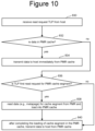
- FIG. 10 is a flow chart describing one embodiment of a process performed a storage system when requested to read data by a host.
- FIG. 11 is a flow chart describing one embodiment of a process performed by a storage system as part of a read process.
- FIG. 12 A depicts a plurality of cache segments and an example order to reading the contents of the cache segments.
- FIG. 12 B depicts the order of issuing TLP read request messages for the embodiment of FIG. 12 A .
- the non-volatile storage system share details of the structure of its storage region and/or the cache with the host.
- the host arranges and sends out requests to read data in a manner that takes advantage of parallelism within the non-volatile storage system.
- a non-volatile storage system implements a persistent memory region (“PMR”) that is accessible by a host.
- PMR persistent memory region
- the non-volatile storage system also implements a PMR cache that includes a plurality of cache segments.
- the non-volatile storage system notifies the host of the size of the cache segments (or other information about the PMR and/or the PMR cache).
- the host uses its knowledge of the size of the cache segments to identify which cache segments of the PMR cache will be used to read the data.
- the host first sends a single read request to the non-volatile storage system for each of the identified cache segments of the PMR cache that will be used to read the data.
- the non-volatile storage system loads the data into the identified cache segments of the PMR cache and returns the requested data to the host.
- the host Upon receipt of the requested data for a cache segment, the host then sends additional read requests for additional data for that respective cache segment. In this manner, all or a portion of the first set of read requests are performed concurrently with each other as well as with all or a portion of the read requests for additional data. This concurrency improves performance of the read process and results in the data read being delivered to the host in a shorter amount of time.
- FIG. 1 A is a block diagram of one embodiment of a storage system 100 connected to a host system 120 .
- Storage system 100 can implement the technology disclosed herein. Many different types of storage systems can be used with the technology disclosed herein. One example storage system is a solid-state drive (“SSD”); however, other types of storage systems can also be used.
- Storage system 100 comprises a memory controller 102 , one or more memory package 104 for storing data, and local memory (e.g. DRAM/ReRAM) 106 .
- Memory controller 102 comprises a Front-End Processor Circuit (FEP) 110 and one or more Back-End Processor Circuits (BEP) 112 .
- FEP 110 circuit is implemented on an ASIC.
- each BEP circuit 112 is implemented on a separate ASIC.
- the ASICs for each of the BEP circuits 112 and the FEP circuit 110 are implemented on the same semiconductor such that the memory controller 102 is manufactured as a System on a Chip (“SoC”).
- SoC System on a Chip
- FEP 110 and BEP 112 both include their own processors.
- FEP 110 and BEP 112 work as a master slave configuration where the FEP 110 is the master and each BEP 112 is a slave.
- FEP circuit 110 implements a flash translation layer that performs memory management (e.g., garbage collection, wear leveling, etc.), logical to physical address translation, communication with the host, management of DRAM (local volatile memory) and management of the overall operation of the SSD (or other non-volatile storage system).
- the BEP circuit 112 manages memory operations in the memory package 104 at the request of FEP circuit 110 .
- the BEP circuit 112 can carry out the read, erase, and programming processes.
- the BEP circuit 112 can perform buffer management, set specific voltage levels required by the FEP circuit 110 , perform error correction (ECC), control the Toggle Mode interfaces to the memory packages, etc.
- ECC error correction
- each BEP circuit 112 is responsible for its own set of memory packages.
- Memory controller 102 is one example of a control circuit.
- each memory package 104 may contain one or more memory dies.
- each memory die in the memory package 104 utilizes NAND flash memory (including two-dimensional NAND flash memory and/or three-dimensional NAND flash memory).
- the memory package 104 can include other types of memory; for example, the memory package can include Phase Change Memory (PCM) memory or Magnetoresistive Random Access Memory (MRAM).
- PCM Phase Change Memory
- MRAM Magnetoresistive Random Access Memory
- memory controller 102 communicates with host system 120 using an interface 130 that implements NVM Express (NVMe) over PCI Express (PCIe).
- host system 120 includes a host processor 122 , host memory 124 , and a PCIe interface 126 , which communicate over bus 128 .
- Host memory 124 is the host's physical memory, and can be DRAM, SRAM, non-volatile memory, or another type of storage.
- Host 120 may also include a hard disk drive connected to bus 128 and/or a USB drive in communication with bus 128 .
- Software (code) for programming host processor 122 can be stored in host memory 124 , a hard disk drive connected to bus 128 or a USB drive.
- Host memory 124 a hard disk drive connected to bus 128 , and a USB drive are examples of non-transitory processor readable storage mediums that store processor readable code that when executed on host processor 122 cause host processor 122 to perform the methods described below.
- Host system 120 is external to and separate from storage system 100 .
- storage system 100 is embedded in host system 120 .
- memory controller 102 may communicate with host 120 via other types of communication buses and/or links, including for example, over an NVMe over Fabrics architecture, or a cache/memory coherence architecture based on Cache Coherent Interconnect for Accelerators (CCIX), Compute Express Link (CXL), Open Coherent Accelerator Processor Interface (OpenCAPI), Gen-Z and the like.
- CCIX Cache Coherent Interconnect for Accelerators
- CXL Compute Express Link
- OpenCAPI Open Coherent Accelerator Processor Interface
- Gen-Z Gen-Z
- FIG. 1 B is a block diagram of one embodiment of FEP circuit 110 .
- FIG. 1 B shows a PCIe interface 150 to communicate with host system 120 and a host processor 152 .
- PCIe interface 150 includes a direct memory access (DMA) module to perform DMA transfers to host memory 124 .
- Host processor 152 can be any type of processor known in the art that is suitable for the implementation.
- Host processor 152 is in communication with a network-on-chip (NOC) 154 .
- NOC network-on-chip
- a NOC is a communication subsystem on an integrated circuit, typically between cores in a SoC. NOC's can span synchronous and asynchronous clock domains or use un-clocked asynchronous logic.
- NOC technology applies networking theory and methods to on-chip communications and brings notable improvements over conventional bus and crossbar interconnections.
- NOC improves the scalability of SoCs and the power efficiency of complex SoCs compared to other designs.
- the wires and the links of the NOC are shared by many signals.
- a high level of parallelism is achieved because all links in the NOC can operate simultaneously on different data packets. Therefore, as the complexity of integrated subsystems keep growing, a NOC provides enhanced performance (such as throughput) and scalability in comparison with previous communication architectures (e.g., dedicated point-to-point signal wires, shared buses, or segmented buses with bridges).
- the DRAM controller 162 is used to operate and communicate with the DRAM (e.g., DRAM 106 , which is a volatile memory).
- SRAM 160 is local volatile RAM memory used by memory processor 156 .
- Memory processor 156 is used to run the FEP circuit and perform the various memory operations.
- Also in communication with the NOC are two PCIe Interfaces 164 and 166 .
- memory controller 102 includes two BEP circuits 112 ; therefore, there are two PCIe Interfaces 164 / 166 . Each PCIe Interface 164 / 166 communicates with one of the BEP circuits 112 . In other embodiments, there can be more or fewer than two BEP circuits 112 ; therefore, there can be more than two PCIe Interfaces.
- a Persistent Memory Region is an area of persistent memory located within storage device 100 that can be accessed by host 120 (e.g., read or write) using standard PCIe commands/transfers, without any of the overhead of command queues that are typical of NVMe.
- An address range is assigned to the PMR for use by the host with standard PCIe commands/transfers.
- the PMR can reside completely in non-volatile memory 104 , completely in volatile memory (e.g., DRAM 106 or SRAM 160 ), or across both non-volatile memory and volatile memory.
- storage device 100 implements a PMR within non-volatile memory 104 , as described below.
- PMR Manager 184 (connected to NOC 154 ), which can be a stand-alone processor (hardwired or programmed by software).
- PMR Manager 184 is a software running on Memory Processor 156 or Host Processor 152 .
- PMR Manager 184 includes PMR Host Access Manager 186 and PMR Cache Manager 188 , both of which can be dedicated electrical circuits, software or a combination of both.
- PMR Host Access Manager 186 manages communication with host 120 .
- Memory Controller 102 implements a PMR cache to locally store a subset of the PMR at the Memory Controller for faster access.
- the PMR cache is implemented in volatile memory such as DRAM 106 or SRAM 160 . More details of the PMR cache will be discussed below.
- PMR Cache Manager 188 manages the PMR cache, reading from non-volatile memory and writing to non-volatile memory 104 .
- FIG. 1 C is a block diagram of one embodiment of the BEP circuit 112 .
- FIG. 1 C shows a PCIe Interface 200 for communicating with the FEP circuit 110 (e.g., communicating with one of PCIe Interfaces 164 and 166 of FIG. 1 B ).
- PCIe Interface 200 is in communication with two NOCs 202 and 204 . In one embodiment the two NOCs can be combined to one large NOC.
- Each NOC ( 202 / 204 ) is connected to SRAM ( 230 / 260 ), a buffer ( 232 / 262 ), processor ( 220 / 250 ), and a data path controller ( 222 / 252 ) via an XOR engine ( 224 / 254 ), an ECC engine ( 226 / 256 ).
- the ECC engines 226 / 256 are used to perform error correction, as known in the art.
- the ECC engines 226 / 256 may be referred to as controller ECC engines.
- the XOR engines 224 / 254 are used to XOR the data so that data can be combined and stored in a manner that can be recovered in case there is a programming error.
- the XOR engines 224 / 254 can recover data that cannot be decoded using ECC engine 226 / 256 .
- Data path controller 222 is connected to a memory interface 228 for communicating via four channels with integrated memory assemblies.
- the top NOC 202 is associated with memory interface 228 for four channels for communicating with memory packages and the bottom NOC 204 is associated with memory interface 258 for four additional channels for communicating with memory packages.
- each memory interface 228 / 258 includes four Toggle Mode interfaces (TM Interface), four buffers and four schedulers. There is one scheduler, buffer, and TM Interface for each of the channels.
- the processor can be any standard processor known in the art.
- the data path controllers 222 / 252 can be a processor, FPGA, microprocessor, or other type of controller.
- the XOR engines 224 / 254 and ECC engines 226 / 256 are dedicated hardware circuits, known as hardware accelerators. In other embodiments, the XOR engines 224 / 254 , ECC engines 226 / 256 can be implemented in software.
- the scheduler, buffer, and TM Interfaces are hardware circuits.
- the memory interface (an electrical circuit for communicating with memory dies) can be a different structure than depicted in FIG. 1 C . Additionally, controllers with structures different than FIGS. 1 B and 1 C can also be used with the technology described herein.
- FIG. 1 D is a block diagram of one embodiment of a memory package 104 that includes a plurality of memory dies 300 (Memory Die 0 , Memory Die 1 , Memory Die 2 , . . . Memory Die M) connected to a memory bus (data lines and chip enable lines) 318 .
- the memory bus 318 connects to a Toggle Mode Interface 270 for communicating with the TM Interface of a BEP circuit 112 (see e.g., FIG. 1 C ).
- the memory package can include a small controller connected to the memory bus 318 and the TM Interface 270 .
- the memory package 104 may have eight or 16 memory die; however, other numbers of memory die can also be implemented.
- the memory package can also include a processor, CPU device, such as a RISC-V CPU along with some amount of RAM to help implement some of capabilities described below.
- a processor, CPU device such as a RISC-V CPU along with some amount of RAM to help implement some of capabilities described below.
- the technology described herein is not limited to any particular number of memory die.
- FIG. 1 E is a block diagram of one embodiment of a volatile memory used with a memory controller 102 .
- the volatile memory of FIG. 1 E is DRAM 106 .
- the non-volatile memory is addressed internally to the memory system using physical addresses associated with one or more memory die.
- the host will use logical addresses to address the various memory locations. This enables the host to assign data to consecutive logical addresses, while the memory system is free to store the data as it wishes among the locations of the one or more memory die.
- the memory controller typically performs translation between the logical addresses used by the host and the physical addresses used by the memory die (“address translation”).
- address translation One example implementation is to maintain data structures that identify the current translation between logical addresses and physical addresses.
- a L2P table is a data structure that identifies translation between logical addresses and physical addresses.
- the L2P table does not need to literally be a table, and many different forms of a data structure can function as and be referred to as a L2P table as long as they enable translation of a logical address to a physical address.
- the one or more data structures that enable translation of logical addresses to physical addresses can be referred to as one L2P table or multiple L2P tables.
- the data structure can be broken up into blocks or other units.
- host 120 can address the non-volatile memory using logical block addresses.
- Memory controller 102 can use its L2P tables to translate between logical block addresses used by host 120 and physical block addresses used within non-volatile memory 104 .
- memory controller 102 uses DRAM 106 to store all or a portion of the L2P tables.
- the memory space of a memory system is so large that DRAM 106 cannot hold all of the L2P tables as well as any other information (besides L2P tables) that DRAM 106 is used to store.
- the entire set of L2P tables are stored in the non-volatile memory 104 and a subset of the L2P tables are cached in the local memory (referred to as L2P cache).
- FIG. 1 E shows DRAM 106 storing L2P cache 282 .
- storage system 100 implements a PMR.
- Memory Controller 102 implements a PMR cache 284 to locally store a subset of the PMR at the Memory Controller for faster access.
- the PMR cache 282 resides in DRAM 106 .
- the L2P tables 282 and the PMR cache 284 reside in SRAM 160 .
- FIG. 1 F is a block diagram of one embodiment of PMR cache 284 that is divided into cache segments.
- FIG. 1 F shows N cache segments: cache segment 0 , cache segment 1 , cache segment 2 , . . . cache segment N ⁇ 1.
- Each cache segment represents a portion of the PMR and stores recently accessed data of the PMR.
- memory controller 102 reads data from the PMR, the data read is first stored in the PMR cache 284 and then transferred to the host. If the data is needed again, then memory controller can access the data from PMR cache 284 rather than reading from the PMR itself, if the data still in the PMR cache.
- each cache segment is of the same size, which is referred to as the cache segment size.
- a subset of the cache segments are sized at a common cache segment size and other cache segments can be of a different size.
- FIG. 2 A is a block diagram that depicts one example of a memory die 300 that can implement the technology described herein.
- Memory die 300 which can correspond to one of the memory die 300 of FIG. 1 C , includes a non-volatile memory array 302 . All or a portion of memory array 302 is used as a PMR 350 .
- PMR 350 resides on one memory die 300 .
- the PMR 350 resides across multiple memory die 300 .
- the array terminal lines of memory array 302 include the various layer(s) of word lines organized as rows, and the various layer(s) of bit lines organized as columns. However, other orientations can also be implemented.
- Memory die 300 includes row control circuitry 320 , whose outputs 308 are connected to respective word lines of the memory array 302 .
- Row control circuitry 320 receives a group of M row address signals and one or more various control signals from System Control Logic circuit 360 , and typically may include such circuits as row decoders 322 , array terminal drivers 324 , and block select circuitry 326 for both reading and writing operations.
- Row control circuitry 320 may also include read/write circuitry.
- Memory die 300 also includes column control circuitry 310 including sense amplifier(s) 330 whose input/outputs 306 are connected to respective bit lines of the memory array 302 .
- Column control circuitry 310 receives a group of N column address signals and one or more various control signals from System Control Logic 360 , and typically may include such circuits as column decoders 312 , array terminal receivers or drivers 314 , block select circuitry 316 , as well as read/write circuitry, and I/O multiplexers.
- System control logic 360 receives data and commands from host 120 and provides output data and status to the controller 102 .
- the system control logic 360 include a state machine 362 that provides die-level control of memory operations.
- the state machine 362 is programmable by software. In other embodiments, the state machine 362 does not use software and is completely implemented in hardware (e.g., electrical circuits). In another embodiment, the state machine 362 is replaced by a micro-controller or microprocessor, either on or off the memory chip.
- the system control logic 360 can also include a power control module 364 that controls the power and voltages supplied to the rows and columns of the memory array 302 during memory operations and may include charge pumps and regulator circuit for creating regulating voltages.
- System control logic 360 includes storage 366 , which may be used to store parameters for operating the memory array 302 .
- Memory controller interface 368 is an electrical interface for communicating with memory controller 102 .
- Examples of memory controller interface 368 include a Toggle Mode Interface and an Open NAND Flash Interface (ONFI). Other I/O interfaces can also be used.
- memory controller interface 368 may implement a Toggle Mode Interface that connects to the Toggle Mode interfaces of memory interface 228 / 258 for memory controller 102 .
- memory controller interface 368 includes a set of input and/or output (I/O) pins that connect to the memory controller 102 .
- all the elements of memory die 300 can be formed as part of a single die. In other embodiments, some or all of the system control logic 360 can be formed on a different die.
- control circuits can include any one or a combination of memory controller 102 , state machine 362 , a micro-controller, micro-processor, all of or a portion of system control logic 360 , row control circuitry 320 , column control circuitry 310 and/or other analogous circuits that are used to control non-volatile memory.
- the one or more control circuits can include hardware only or a combination of hardware and software (including firmware).
- firmware for example, a controller programmed by firmware to perform the functions described herein is one example of a control circuit.
- a control circuit can include a processor, FGA, ASIC, integrated circuit, or other type of circuit.
- memory structure 302 comprises a three-dimensional memory array of non-volatile memory cells in which multiple memory levels are formed above a single substrate, such as a wafer.
- the memory structure may comprise any type of non-volatile memory that are monolithically formed in one or more physical levels of memory cells having an active area disposed above a silicon (or other type of) substrate.
- the non-volatile memory cells comprise vertical NAND strings with charge-trapping layers.
- memory structure 302 comprises a two-dimensional memory array of non-volatile memory cells.
- the non-volatile memory cells are NAND flash memory cells utilizing floating gates.
- Other types of memory cells e.g., NOR-type flash memory can also be used.
- memory array architecture or memory cell included in memory structure 302 is not limited to the examples above. Many different types of memory array architectures or memory technologies can be used to form memory array 302 . No particular non-volatile memory technology is required for purposes of the new claimed embodiments proposed herein.
- Other examples of suitable technologies for memory cells of the memory array (or other type of memory structure) 302 include ReRAM memories (resistive random access memories), magnetoresistive memory (e.g., MRAM, Spin Transfer Torque MRAM, Spin Orbit Torque MRAM), FeRAM, phase change memory (e.g., PCM), and the like. Examples of suitable technologies for memory cell architectures include two dimensional arrays, three dimensional arrays, cross-point arrays, stacked two dimensional arrays, vertical bit line arrays, and the like.
- a ReRAM cross-point memory includes reversible resistance-switching elements arranged in cross-point arrays accessed by X lines and Y lines (e.g., word lines and bit lines).
- the memory cells may include conductive bridge memory elements.
- a conductive bridge memory element may also be referred to as a programmable metallization cell.
- a conductive bridge memory element may be used as a state change element based on the physical relocation of ions within a solid electrolyte.
- a conductive bridge memory element may include two solid metal electrodes, one relatively inert (e.g., tungsten) and the other electrochemically active (e.g., silver or copper), with a thin film of the solid electrolyte between the two electrodes.
- the conductive bridge memory element may have a wide range of programming thresholds over temperature.
- MRAM magnetoresistive random access memory
- the elements are formed from two ferromagnetic layers, each of which can hold a magnetization, separated by a thin insulating layer.
- One of the two layers is a permanent magnet set to a particular polarity; the other layer's magnetization can be changed to match that of an external field to store memory.
- a memory device is built from a grid of such memory cells. In one embodiment for programming, each memory cell lies between a pair of write lines arranged at right angles to each other, parallel to the cell, one above and one below the cell. When current is passed through them, an induced magnetic field is created.
- MRAM based memory embodiments will be discussed in more detail below.
- Phase change memory exploits the unique behavior of chalcogenide glass.
- One embodiment uses a GeTe—Sb2Te3 super lattice to achieve non-thermal phase changes by simply changing the co-ordination state of the Germanium atoms with a laser pulse (or light pulse from another source). Therefore, the doses of programming are laser pulses.
- the memory cells can be inhibited by blocking the memory cells from receiving the light.
- the memory cells are programmed by current pulses. Note that the use of “pulse” in this document does not require a square pulse but includes a (continuous or non-continuous) vibration or burst of sound, current, voltage light, or other wave.
- These memory elements within the individual selectable memory cells, or bits may include a further series element that is a selector, such as an ovonic threshold switch or metal insulator substrate.
- FIG. 2 A can be grouped into two parts, the structure of memory array 302 and the peripheral circuitry, which (in some embodiments) includes all of the structures 310 , 320 and 360 other than memory array 302 .
- An important characteristic of a memory circuit is its capacity, which can be increased by increasing the area of the memory die of storage system 100 that is given over to the memory structure 302 ; however, this reduces the area of the memory die available for the peripheral circuitry. This can place quite severe restrictions on these peripheral elements. For example, the need to fit sense amplifier circuits within the available area can be a significant restriction on sense amplifier design architectures. With respect to the system control logic 360 , reduced availability of area can limit the available functionalities that can be implemented on-chip. Consequently, a basic trade-off in the design of a memory die for the storage system 100 is the amount of area to devote to the memory structure 302 and the amount of area to devote to the peripheral circuitry.
- CMOS complementary metal-oxide-semiconductor
- elements such sense amplifier circuits, charge pumps, logic elements in a state machine, and other peripheral circuitry in system control logic 360 often employ PMOS devices. Processing operations for manufacturing a CMOS die will differ in many aspects from the processing operations optimized for an NMOS flash NAND memory or other memory cell technologies.
- the memory array 302 can be formed on one die (the memory die) and some or all of the peripheral circuitry elements, including one or more control circuits, can be formed on a separate die (the control die).
- a memory die can be formed of just the memory elements, such as the array of memory cells of flash NAND memory, MRAM memory, PCM memory, ReRAM memory, or other memory type.
- Some or all of the peripheral circuitry, even including elements such as decoders and sense amplifiers, can then be moved on to a separate control die. This allows each of the memory die to be optimized individually according to its technology.
- a NAND memory die can be optimized for an NMOS based memory array structure, without worrying about the CMOS elements that have now been moved onto a separate peripheral circuitry die that can be optimized for CMOS processing. This allows more space for the peripheral elements, which can now incorporate additional capabilities that could not be readily incorporated were they restricted to the margins of the same die holding the memory cell array.
- the two die can then be bonded together in a bonded multi-die memory circuit, with the array on the one die connected to the periphery elements on the other memory circuit.
- FIG. 2 B shows an alternative arrangement to that of FIG. 2 A which may be implemented using wafer-to-wafer bonding to provide a bonded die pair.
- FIG. 2 B depicts a functional block diagram of one embodiment of an integrated memory assembly 307 .
- One or more integrated memory assemblies 307 may be used in a memory package 104 in storage system 100 .
- the integrated memory assembly 307 includes two types of semiconductor die (or more succinctly, “die”).
- Memory die 301 includes memory array 302 .
- Memory array 302 may contain non-volatile memory cells. All or a portion of memory array 302 is used as a PMR 350 .
- PMR 350 resides in memory array 302 on memory die 301 of integrated memory assembly 307 .
- PMR 350 resides within one memory array or within one memory die.
- the PMR 350 resides across multiple memory die 300 and/or across multiple integrated memory assemblies 307 .
- Control die 311 includes control circuitry 310 , 320 and 360 (details of which are discussed above). In some embodiments, control die 311 is configured to connect to the memory array 302 in the memory die 301 .
- FIG. 2 B shows an example of the peripheral circuitry, including control circuits, formed in a peripheral circuit or control die 311 coupled to memory array 302 formed in memory die 301 . Common components are labelled similarly to FIG. 3 A .
- System control logic 360 , row control circuitry 320 , and column control circuitry 310 are located in control die 311 . In some embodiments, all or a portion of the column control circuitry 310 and all or a portion of the row control circuitry 320 are located on the memory die 301 . In some embodiments, some of the circuitry in the system control logic 360 is located on the on the memory die 301 .
- System control logic 360 , row control circuitry 320 , and column control circuitry 310 may be formed by a common process (e.g., CMOS process), so that adding elements and functionalities, such as ECC, more typically found on a memory controller 102 may require few or no additional process steps (i.e., the same process steps used to fabricate controller 102 may also be used to fabricate system control logic 360 , row control circuitry 320 , and column control circuitry 310 ).
- CMOS process complementary metal-oxide
- FIG. 2 B shows column control circuitry 310 including sense amplifier(s) 350 on the control die 311 coupled to memory array 302 on the memory die 301 through electrical paths 306 .
- electrical paths 306 may provide electrical connection between column decoder 312 , driver circuitry 314 , and block select 316 and bit lines of memory array (or structure) 302 .
- Electrical paths may extend from column control circuitry 310 in control die 311 through pads on control die 311 that are bonded to corresponding pads of the memory die 301 , which are connected to bit lines of memory structure 302 .
- Each bit line of memory structure 302 may have a corresponding electrical path in electrical paths 306 , including a pair of bond pads, which connects to column control circuitry 310 .
- row control circuitry 320 including row decoder 322 , array drivers 324 , and block select 326 are coupled to memory array 302 through electrical paths 308 .
- Each of electrical path 308 may correspond to a word line, dummy word line, or select gate line. Additional electrical paths may also be provided between control die 311 and memory structure die 301 .
- control die 311 there is more than one control die 311 and/or more than one memory die 301 in an integrated memory assembly 307 .
- the integrated memory assembly 307 includes a stack of multiple control die 311 and multiple memory structure die 301 .
- each control die 311 is affixed (e.g., bonded) to at least one of the memory structure dies 301 .
- FIG. 3 depicts an example of a metablock that resides across M dies (Dies 0 , Die 1 , . . . Die M ⁇ 1).
- each memory die includes two planes of memory cells (Plane 0 and Plane 1 ).
- each memory die includes one plane of memory cells or more than two planes of memory cells. The exact number of planes is not limited for the technology described herein.
- each plane includes X+1 physical blocks of memory cells (block 0 , block 1 , . . . block X).
- memory controller groups physical blocks from each plane into a metablock. For example, FIG.
- each block includes a set of word lines connecting to all of the NAND strings of that block.
- Each block also includes a set of bit lines such that one bit line connects to a subset of NAND strings for that block (e.g., one bit line connects to one NAND string, four NAND strings, six NAND strings, eight NAND strings, etc., depending on the architecture).
- the unit of erase is a physical block. That is, an entire physical block is erased at the same time.
- the unit of programming and the unit of reading is a physical page. That is, a physical page represents the number of data bits programmed or read concurrently.
- a physical page includes all data stored in all memory cells of a same physical block that are connected to a same word line.
- a physical page includes a subset of data stored in all memory cells of a same physical block that are connected to a same word line.
- a physical page may include data stored in % (or other fraction) of the memory cells of a same physical block that are connected to a same word line.
- a physical page is equal to 4 KB.
- the memory controller can write data to and read data from a metapage such that a metapage includes a physical page from each physical block of a metablock.
- a metapage includes a physical page from each physical block of a metablock.
- the metapage comprises pages from M*2 physical blocks and, therefore, stores M*2*4 KB of data.
- PMR cache 284 includes a set of cache segments.
- each cache segment stores data from one metapage.
- each cache segment has a cache segment size of M*2*4 KB.
- a cache segment can store data for one page from one physical block, from multiple metapages, or other amounts.
- storage system 100 implements a PMR that can be accessed by host 120 (e.g., read or write) using standard PCIe commands.
- a commands is included in a Transaction Layer Packet (“TLP”), which refers to the transaction layer of the PCIe communications mechanism (transaction layer, data link layer and physical layer).
- TLP Transaction Layer Packet
- two packets are involved: one TLP (e.g., the read request TLP) from the host 120 to the storage system 100 asking the latter to perform a read operation, and one TLP (e.g., the completion TLP) going back from storage system 100 to host 120 with the data.
- the TLP (the read request TLP) from the host 120 to the storage system 100 asking the latter to perform a read operation is depicted in FIG. 4 A .
- the TLP (the completion TLP) going back from storage system 100 to host 120 with the data is depicted in FIG. 4 B .
- the read request TLP depicted in FIG. 4 A is generated by the host 120 (e.g., host processor 122 or a memory controller chipset of the host or another component of the host), which is sometimes referred to as the Root Complex.
- the fields of the read request TLP are:
- storage device 100 When storage device 100 (e.g., memory controller 102 ) receives a Read Request TLP, it responds with a completion TLP. That is, storage device 100 reads the chunk of data from PMR 350 and returns the result back to host 120 . That result includes the completion TLP depicted in FIG. 4 B .
- the fields of the completion TLP are:
- host 120 sends read request TLPs for 256 bytes of data, which is 64 double words, so the Length field of the read request TLP is set to 64. In another embodiment, host 120 sends read request TLPs for 512 bytes of data, which is 128 double words, so the Length field of the read request TLP is set to 128. In other embodiments, the host can send read requests for different amounts of data. The amount of data requested by a read request TLP is referred to herein as a TLP unit of data.
- each cache segment of PMR cache 284 has a cache segment size of M*2*4 KB (where M is the number of dies).
- M is the number of dies.
- the cache segment size is (16*2*4 KB) 128 KB, which is significantly larger than the amount of data requested in a TLP unit of data.
- the cache segment size is 64 KB.
- the TLP unit of data is smaller than the cache segment size such that multiple TLP units of data fit within one cache segment.
- the host is typically not aware of the how the PMR cache is structured and operated, and host side application that use the PMR are not optimized for how the non-volatile memory is managed, host side application may access the PMR inefficiently (e.g., not take advantage of parallelism in the storage system, thereby reducing performance). For example, a loop which iterates over a large buffer in the PMR and performs a transformation on each double word within the buffer will create individual memory accesses for each double word thus flooding the PCIe link with tiny requests.
- FIG. 5 A depicts a plurality of cache segments and provides an example of a host (that is not using the technology proposed herein) accessing the PMR inefficiently (e.g., not take advantage of parallelism in the storage system, thereby reducing performance).
- FIG. 5 A shows four cache segments: cache segment 0 , cache segment 1 , cache segment 2 and cache segment 3 .
- Four cache segments are depicted for example purposes only.
- a PMR cache is likely to have more than four cache segments. The exact number of cache segments is implementation dependent.
- each cache segment stores the equivalent of 128 TLP units of data.
- FIG. 5 A labels the data in the cache segments based on the order that the host is requesting the TLP unit of data, for this example.
- the first TLP unit of data requested by the host is labeled dTLP 0
- the second TLP unit of data requested by the host is labeled dTLP 1
- the third TLP unit of data requested by the host is labeled dTLP 2
- . . . the five hundred and twelfth TLP unit of data requested by the host is labeled dTLP 511 .
- the order of that the host requests the TLP units of data is graphically depicted in order by arrows 470 , 472 , 474 , 476 , 478 , 480 and 482 .
- TLP 0 requests dTLP 0
- TLP 1 requests dTLP 1
- TLP 2 requests dTLP 2 , etc.
- PMR Host Access Manager 186 When storage system 100 receives TLP 0 (a read request TLP), PMR Host Access Manager 186 translates the address in TLP 0 to an LBA (logical block address) and sends that LBA to memory processor 156 (see FIG. 1 B ) to determine the appropriate physical addresses in the non-volatile memory. Controller 120 will read an entire metapage from the non-volatile memory and store that metapage in cache segment 0 as dTLP 0 , dTLP 1 , . . . dTLP 127 . When the data in cache segment 0 is stored, then dTLP 0 is returned (from cache segment 0 rather than from the non-volatile memory) in a completion TLP in response to TLP 0 .
- LBA logical block address
- TLP 128 When TLP 128 is received, the data for that TLP (ie dTLP 128 ) will not already be in the PMR cache; therefore, storage system 100 will need to read the data from non-volatile memory and load it into the PMR cache. However, as discussed above, storage system will not just read the data requested by TLP 128 . Rather, storage system will read a metapage of data and fill cache segment 1 with that metapage resulting in dTLP 128 -dTLP 255 being stored in cache segment 1 . So the read request embodied in TLP 128 will have to wait while cache segment 1 is being loaded. TLP 256 and TLP 384 will experience the same delays, as they wait for the next metapage to be loaded into the PMR cache. Thus, every time a TLP crosses a metapage boundary, or a cache segment boundary, there is a pause or delay in sending out completion TLPs with the requested data. This pause slows down the read process performance.
- storage system 100 share details of the structure of PMR 350 and/or PMR cache 284 with the host.
- host 120 can arrange and send out read request TLPs in a manner that takes advantage of parallelism within storage system 100 .
- One example of a detail of PMR 350 and/or PMR cache 284 is the cache segment size. If host 120 is aware of the cache segment size, it can send read requests in a manner that is more efficient than described above with respect to FIG. 5 A , For example, host 120 can take advantage of the parallelism built into storage system 100 . More details are provided below with respect to FIGS. 6 - 12 B .
- FIG. 6 is a flow chart describing one embodiment of a process for reading data.
- non-volatile storage system 100 that is implementing a storage region (e.g., PMR) which is accessible to a host 120 and a cache for the storage region (e.g., PMR cache) shares details of the structure of the storage region and/or the cache with host 120 .
- storage system 100 informs host 120 of the cache segment size.
- PMR storage region
- other types of storage regions can also be used with the technology described herein.
- step 504 with awareness of the shared details of the structure of the storage region and/or the cache, host 120 arranges and sends out requests to read data (e.g., read request TLPs) in a manner that takes advantage of parallelism within non-volatile storage system 100 .
- step 506 data is read from storage system 100 taking advantage of the parallelism within storage system 100 due to the host's arrangement of the requests to read data.
- host 120 can send out read request TLPs for the different cache segments in advance of sending out the bulk of the read request TLPs.
- the host will initially issue only a single TLP for each cache segment.
- host 120 will send out the additional read request TLPs.
- TLP 0 TLP 128 , TLP 256 and TLP 384 to storage system 100 .
- storage system 100 Upon receipt of TLP 0 , TLP 128 , TLP 256 and TLP 384 , storage system 100 will read the data for cache segment 0 , cache segment 1 , cache segment 2 and cache segment 3 and load the data (dTLP 1 . dTLP 1 , . . . dTLP 511 ) into the respective cache segments.
- Responding to TLP 0 causes storage system 100 to read a full metapage that includes dTLP 0 , dTLP 1 , . . . dTLP 127 and load that data into cache segment 0 .
- Responding to TLP 128 causes storage system 100 to read a full metapage that includes dTLP 128 , dTLP 129 , . . . dTLP 255 and load that data into cache segment 1 .
- Responding to TLP 256 causes storage system 100 to read a full metapage that includes dTLP 256 , dTLP 257 , . . . dTLP 383 and load that data into cache segment 2 .
- Responding to TLP 384 causes storage system 100 to read a full metapage that includes dTLP 384 , dTLP 385 , . . . dTLP 511 and load that data into cache segment 3 .
- the process of reading and loading the data for cache segment 0 , cache segment 1 , cache segment 2 and cache segment 3 is performed in parallel (concurrently) by storage system 100 .
- the process of reading and loading the data for cache segment 0 , cache segment 1 , cache segment 2 and cache segment 3 is performed serially. Even if performed serially, the data for cache segment 1 is likely to be loaded into cache segment 1 prior to storage system 100 receiving TLP 129 .
- FIG. 7 is a flow chart describing one embodiment of a process for reading data.
- the process of FIG. 7 is an example implementation of the process of FIG. 6 .
- the process of FIG. 7 is performed by host 120 .
- host 120 accesses an indication of the cache segment size for non-volatile storage system 100 , which is implementing a storage region (e.g., PMR 350 ) and a cache for the storage region (e.g. PMR cache 284 ).
- the cache comprises a plurality of cache segments that are each sized at a cache segment size.
- storage system 100 sends the cache segment size to host 120 at the time that storage system 100 is powered on and/or initialized.
- storage system 100 sends the cache segment size to host 120 periodically or at a time different than initialization. In another embodiment, storage system 100 sends the cache segment size to host 120 in response to a request from host 120 . In yet another embodiment, host 120 determines what the cache segment size should be and informs storage system 100 of that cache segment size. In yet another embodiment, storage system 100 stores an indication of the cache segment size in a known location for host 120 to read. Other variations can also be implemented.
- step 552 based on the indication of a cache segment size, host 120 determines a set of cache segments of the plurality of cache segments that will be used by storage system 100 for reading a set of data. For example, if host 120 needs to read the data labeled in FIG. 5 A as dTLP 256 -dTLP 390 , then host 120 determines that cache segment 2 and cache segment 3 will be used by storage system 100 for reading the requested data. By knowing the cache segment size, host 120 can determine which cache segments corresponds to which pages or metapages of data. In one embodiment, storage system 100 can also inform host 120 of the correspondence between cache segments and address ranges of the PMR. In another embodiment, different cache segments can have different sizes and storage system 100 will inform host 120 about which cache segments have which size.
- step 554 host 120 sends an initial read request for each cache segment of the set of cache segments corresponding to data from the set of data. For example, looking at FIG. 5 A , host 120 initially sends TLP 0 , TLP 128 , TLP 256 and TLP 384 to storage system 100 in step 554 . In the example above where host 120 only needs dTLP 256 -dTLP 390 , then host 120 will send TLP 256 and TLP 384 to storage system 100 in step 554 .
- TLP 0 In the example host 120 will initially send TLP 0 , TLP 128 , TLP 256 and TLP 384 to storage system 100 in step 554 , storage system will respond to those four TLPs by reading the data for dTLP 0 -dTLP 511 , loading that data into cache segments 0 - 3 , and sending four completion TLPs to host 120 (one completion TLP in response to TLP 0 , one completion TLP in response to TLP 128 , one completion TLP in response to TLP 256 , and one completion TLP in response to TLP 384 ).
- the completion TLP in response to TLP 0 will include dTLP 0 .
- the completion TLP in response to TLP 128 will include dTLP 128 .
- the completion TLP in response to TLP 256 will include dTLP 256 .
- the completion TLP in response to TLP 384 will include dTLP 384 .
- step 556 after sending the initial read request for each cache segment of the set of cache segments, host 120 sends additional read requests for additional data in the cache segments corresponding to the set of data.
- Each of the read requests is for a unit of data (e.g., TLP unit of data).
- the TLP unit of data is smaller than the cache segment size such that multiple TLP units of data fit within one cache segment.
- FIGS. 8 - 11 are flow charts that together describe one embodiment of a process for reading data.
- the process of FIGS. 8 - 11 is an example implementation of the process of FIG. 6 .
- the process of FIGS. 8 - 11 is also an example implementation of the process of FIG. 7 .
- FIGS. 8 , 10 and 11 describe operation of storage system 100 .
- FIG. 9 describe operation of host 120 .
- step 602 of FIG. 8 storage system 100 is powered on and/or is reset.
- step 604 storage system 100 is initialized.
- step 606 storage system shares the cache segment size of PMR cache 284 with host 120 . This sharing of the cache segment size can be performed using any of the methods described above.
- step 608 storage system is operated with PMR 350 implemented.
- PMR 350 is implemented to allow direct memory-level access and PMR 350 is mapped to host memory 124 such that a direct pointer-type read or write can be performed.
- Steps 704 - 722 of FIG. 9 , the process of FIG. 10 and the process of FIG. 11 are all performed as part of step 608 of FIG. 8 .
- FIG. 9 describes the operation of host 120 when reading PMR 350 .
- Step 702 of FIG. 9 includes host 120 receiving the cache segment size for PMR cache 284 . This sharing of the cache segment size can be performed using any of the methods described above. Host 120 can also receive other details of PMR 350 and PMR cache 284 , as described above. Host 120 may receive one cache segment size or multiple cache segment sizes, as described above.
- Step 720 of FIG. 9 is performed in response to step 606 of FIG. 8 .
- step 704 of FIG. 9 host 120 determines that a set of data needs to be read from PMR 350 and determines addresses in the PMR for that data. In one embodiment, those addresses are in the host memory address space.
- step 706 based on the cache segment size, host 120 determines the set of cache segments that will be used by storage system 100 for reading the set of data. Step 706 is analogous to step 552 .
- step 708 host 120 generates and sends a first read request TLP (a read request TLP is an example of a read request) for each cache segment that will be used by the storage system for reading the set of data.
- a read request TLP requests the reading of a TLP unit of data, which is smaller than the cache segment size such that multiple TLP units of data fit within one cache segment.
- the host initially sends TLP 0 , TLP 128 , TLP 256 and TLP 384 to storage system 100 .
- different TLPs can be sent as long as the host sends at least one TLP for each cache segment that will be used by the storage system for reading the set of data.
- host 120 can also send any one of TLP 0 -TLP 127 , any one of TLP 128 -TLP 255 , any one of TLP 256 -TLP 383 and any one of TLP 384 -TLP 511 .
- host 120 sends TLP 4 , TLP 135 , TLP 300 and TLP 414 in step 708 .
- the host sends one read request for each cache segment of the set of the cache segments that will be used by the storage system for reading the set of data.
- host can send more than one read request for each cache segment of the set of the cache segments that will be used by the storage system for reading the set of data.
- step 710 host 120 monitors for receipt of completion TLPs that are sent to host 120 in response to the first read request TLPs sent by host 120 in step 708 .
- host 120 determines whether a completion TLP is received for the current cache segment being operated on. If not, host 120 continues to wait. If host 120 has received the completion TLP for the current cache segment, host 120 will send out additional read request TLPs for the current cache segment in steps 714 - 716 .
- step 704 host needs to read dTLP 0 -dTLP 511 (step 704 ) and determines that cache segments 0 - 3 will be used by storage system 100 to read that data (step 706 ), then in step 708 host 120 will send out only TLP 0 , TLP 128 , TLP 256 and TLP 384 to storage system 100 . After host 120 sends the one read request TLP for each cache segment of the set of cache segments, host 120 will send the additional read requests (e.g., TLP 1 -TLP 127 , TLP 129 -TLP 255 , TLP 257 -TLP 383 and TLP 385 -TLP 511 ).
- additional read requests e.g., TLP 1 -TLP 127 , TLP 129 -TLP 255 , TLP 257 -TLP 383 and TLP 385 -TLP 511 ).
- the additional read request TLPs are sent out sequentially. Therefore, first the additional read request TLPs are sent out for cache segment 0 . So the first time step 714 is performed for this read process, the “current cache segment” is cache segment 0 and host 120 determines whether it has received the completion TLP for TLP 0 (or which first read request for cache segment 0 was sent out in step 708 ).
- step 714 host 120 generates and sends an additional read request TLP for the next TLP unit of data for the current cache segment.
- step 714 includes generating and sending out TLP 1 .
- step 716 host determines whether there are more TLP units of data to request for the current cache segment. If the last TLP sent out was TLP 1 , then the answer is yes and the process loops back to step 714 so TLP 2 can be sent out. And so on, until all read request TLPs for the current cache segment have been sent out (e.g., TLP 0 -TLP 127 have all been sent out).
- step 718 host 120 determines if there are more cache segments that need to be read from. If not, then the read process is complete and the data read is stored in host memory 124 (sept 722 ). If there are more cache segments that need to be read from then host 120 will proceed to start reading the additional data from the next cache segment (step 720 ) and the process loops back to step 714 to start reading additional data from the new current cache segment.
- Steps 714 - 722 comprise sending additional read requests for individual cache segments of the set of cache segments after receiving at least one completion message for the respective cache segment in response to a respective read request of the initial read request for each cache segment.
- host reads data from the cache segments in order from cache segment 0 to cache segment 3 .
- host 120 can read the data in other orders.
- host 120 does not start sending additional read request TLPs for a cache segment until host 120 receives at least one completion TLP for that cache segment. This is because when host 120 receives at least one completion TLP for that cache segment, host 120 then knows that all of the data for that cache segment has been loaded into the PMR cache.
- host 120 can implement a timer that determines when a predetermined period of time has elapsed since sending out the first read request TLP for each cache segment in step 708 . When that predetermined period of time has elapsed, the additional read request TLPs of step 714 can be sent out.
- the predetermined period of time could be the sum of the time needed to read from the non-volatile memory, the time needed to load the data read into the PMR cache, and the time needed to communicate a completion TLP.
- Other predetermined periods can also be used.
- step 714 can start to be performed for cache segment 0 and dTLP 1 after waiting for the predetermined time period following the sending the initial read requests (TLP 0 , TLP 128 , TLP 256 and TLP 384 ) for each cache segment.
- step 714 can start to be performed for cache segment 0 and dTLP 1 after waiting for the predetermined time period following the sending the initial read request TLP 0 for each cache segment 0 .
- FIG. 10 describes operation of storage system 100 .
- the process of FIG. 10 is performed multiple times in order for the storage system to read the set of data from the PMR and load the set of data into the set of the cache segments.
- storage system 100 receives a read request TLP from host 100 .
- Step 830 can be performed in response to step 708 of FIG. 9 .
- step 708 of FIG. 9 may include sending out more than one read request TLPs.
- step 708 may include sending out read requests TLP 0 , TLP 128 , TLP 256 and TLP 384 . In that case, storage system may perform the process of FIG. 10 four times concurrently.
- step 830 is performed for each of read requests TLP 0 , TLP 128 , TLP 256 and TLP 384 by starting four instances of the process of FIG. 10 that are performed concurrently.
- the term “concurrently” is used to mean that two or more events/processes/tasks are happening during at least one common moment in time, even if they start and stop at different times.
- storage system 100 may read a first group of data from the PMR and load that first group of data into cache segment 0 concurrently with storage system 100 reading a second group of data from the PMR and loading that second group of data into second cache segment 1 , even if the reading of the first group of data started slightly before the reading of the second group of data because from the start of the reading of the second group of data until the completion of the loading of the first group of data into cache segment 0 , both processes were running.
- step 832 storage system 100 determines whether the data requested by the read request received in step 830 is already stored in PMR cache 284 . If so, then in step 834 that the data requested by the read request received in step 830 is transmitted from the PMR cache 284 to host 120 as part of a completion TLP. If the data requested by the read request received in step 830 is not already stored in PMR cache 284 , then (in step 836 ) storage system 100 determines whether the read request received in step 830 is the first read request for the relevant cache segment in PMR cache 284 .
- step 838 includes storage system reading a metapage of data and storing that metapage in a cache segment.
- reading the metapage comprises the memory controller reading a physical page of data from each of multiple memory dies and aggregating the physical pages of data to form a meta page which corresponds to a cache segment of data.
- step 836 storage system 100 determined that the TLP being considered in step 836 is not the first read request for the relevant cache segment in PMR 284 , then the storage system has already started the process to fill the relevant cache segment and does not need to start another operation to read form non-volatile memory. Rather, storage system 100 will wait until the appropriate cache segment is loaded with the data read in step 838 , and then the data requested in the current read request TLP being processed is transmitted to host 120 in a completion TLP as part of step 840 .
- step 836 is being performed by sending TLP 128 , then TLP 128 is the first read request for the relevant cache segment in PMR cache 284 ; therefore, the process continues to step 838 to read from PMR 350 the metapage that includes dTLP 128 -dTLP 255 and store that data in cache segment 1 .
- step 836 is being performed by TLP 129 , then the storage system can determine that TLP 129 is not the first read request for the relevant cache segment in PMR cache 284 because TLP 128 was already received; therefore, the process continues to step 840 so that the storage system can wait until cache segment 1 is fully loaded to transmit dTLP 129 to host 120 in a completion TLP.
- FIG. 10 demonstrates that when storage system 100 receives the first read request for a cache segment, it reads the data for the cache segment from the PMR in non-volatile memory, loads the data in the cache segment and returns the requested data to host 120 .
- storage system 100 receives additional read requests, after the initial/first read request for the cache segment, storage system returns additional data to host 120 in response to the additional read requests by reading the additional data from the appropriate cache segment(s) and transmitting the additional data read to host 120 .
- FIG. 11 is a flow chart describing one embodiment of a process for reading a metapage of data from PMR 350 in non-volatile memory and storing the data for that metapage into a cache segment of PMR cache 284 .
- the process of FIG. 11 is an example implementation of step 838 of FIG. 10 .
- PMR manager 184 converts the PMR address from the read request TLP to a set of LBAs for all of the data in the metapage that includes the data requested in the read request TLP.
- Those LBAs are provided to memory processor 156 , which implements a flash translation layer that translates the LBAs to physical addresses in the non-volatile memory in step 904 .
- PMR 350 can also point to physical addresses in non-volatile memory and not logical addresses; for example, the data might have originally been written using a sequential pattern such as ZNS and as such not require individual logical addressing at the PMR level since the data is always sequential and parallel within the memory dies.
- memory processor 156 or processor 220 or another processor
- step 906 memory processor 156 (or processor 220 or another processor) will build one or more read commands to concurrently read data for the metapage from one or more planes on one or more memory die. If the bus between memory controller 102 and non-volatile memory 104 (see channels for communicating with Memory Package depicted in FIG. 1 C ) is busy and not available to transfer additional data (step 908 ), then memory controller 102 will wait until the bus is available.
- step 910 the appropriate BEP 112 will send the one or more read commands to one or more memory die so that the data of the metapage is concurrently read from one or more planes on one or more die that comprise the PMR.
- step 912 memory controller 102 receives the data for the metapage that was sensed from one or more planes on one or more die.
- step 914 that data is decoded to remove error correction information (e.g., extra parity bits) and recover the original data.
- step 916 the data read for the metapage is loaded into the appropriate cache segment.
- FIG. 12 A depicts a plurality of cache segments and provides an example of efficiently reading the PMR according to the processes of FIGS. 8 - 11 .
- FIG. 12 A shows four cache segments: cache segment 0 , cache segment 1 , cache segment 2 and cache segment 3 .
- Four cache segments are depicted for example purposes only.
- a PMR cache is likely to have more than four cache segments. The exact number of cache segments is implementation dependent.
- each cache segment stores the equivalent of 128 TLP units of data. Note that the reference labels for the data in the cache segments is made to match the reference labels of FIG. 5 A , but in the example of FIG. 12 A the reference labels for the data is not based on the order that the host requests the TLP units of data.
- FIG. 12 B depicts the read request TLPs in the order that they are issued by host 120 for this example.
- storage system 100 informed host 120 of the cache segment size (see step 702 of FIG. 9 ), host 120 determined that the set of data dTLP 0 -dTLP 511 needs to be read from PMR 350 (see step 704 of FIG. 9 ) and host 120 used the cache segment size to determine a set of the cache segments (cache segment 0 , cache segment 1 , cache segment 2 and cache segment 3 ) that will be used by storage system 100 for reading the set of data (see step 706 of FIG. 9 ).
- Host 120 first sends at least one read request TLP for each cache segment of the set of the cache segments that will be used by the storage system for reading the set of data (see step 708 of FIG. 9 ).
- FIG. 12 B shows that the first four read request TLPs sent by host 120 are TLP 0 , TLP 128 , TLP 256 and TLP 384 . So this initial set of read request TLPs includes exactly one TLP for each cache segment of the set of the cache segments that will be used by the storage system for reading the set of data.
- storage system 100 In response to the initial set of read request TLPs (TLP 0 , TLP 128 , TLP 256 and TLP 384 ), storage system 100 reads at least a portion of the set of data from PMR 350 (e.g., all of the set of data or a subset of the set of data) and loads that portion of the set of data into the set of the cache segments in response to the at least one read request for each cache segment of the set of cache segments. For example, in response to receiving TLP 0 , TLP 128 , TLP 256 and TLP 384 , storage system 100 performs the process of FIG.
- storage system 100 determines that dTLP 0 is not in PMR cache 284 (step 832 ) and that TLP 0 is the first read request for PMR cache segment 0 (see step 836 ); therefore, storage system 100 reads dTLP 0 -dTLP 127 from PMR 250 (in non-volatile memory) and loads dTLP 0 -dTLP 127 into cache segment 0 (see step 838 ).
- storage system 100 determines that dTLP 128 is not in PMR cache 284 (step 832 ) and that TLP 128 is the first read request for PMR cache segment 1 (see step 836 ); therefore, storage system 100 reads dTLP 128 -dTLP 255 from PMR 250 (in non-volatile memory) and loads dTLP 128 -dTLP 255 into cache segment 0 (see step 838 ).
- storage system 100 determines that dTLP 256 is not in PMR cache 284 (step 832 ) and that TLP 256 is the first read request for PMR cache segment 2 (see step 836 ); therefore, storage system 100 reads dTLP 256 -dTLP 383 from PMR 250 (in non-volatile memory) and loads dTLP 256 -dTLP 383 into cache segment 2 (see step 838 ).
- storage system 100 determines that dTLP 384 is not in PMR cache 284 (step 832 ) and that TLP 384 is the first read request for PMR cache segment 3 (see step 836 ); therefore, storage system 100 reads dTLP 384 -dTLP 511 from PMR 250 (in non-volatile memory) and loads dTLP 384 -dTLP 511 into cache segment 3 (see step 838 ).
- the initial set of read request TLPs can be TLPs other than TLP 0 , TLP 128 , TLP 256 and TLP 384 .
- the host needs to send at least one TLP for each relevant cache segment. Therefore, the initial set of read request TLPs can include, for example, TLP 5 , TLP 129 , TLP 383 and TLP 440 as this set includes at least one TLP for each relevant cache segment.
- Storage system 100 sends initial data back to host 120 using completion TLPs in response to one or more of the at least one read request for each cache segment of the set of cache segments. This initial data is sent from PMR cache 284 after the respective metapage is loaded into the respective cache segment of PMR cache 284 .
- response TLP 0 storage system transmits dTLP 0 to host 120 after dTLP 0 -dTLP 127 are loaded into cache segment 0 ; in response TLP 128 storage system transmits dTLP 128 to host 120 after dTLP 128 -dTLP 255 are loaded into cache segment 1 ; in response TLP 256 storage system transmits dTLP 256 to host 120 after dTLP 256 -dTLP 383 are loaded into cache segment 2 ; and in response TLP 384 storage system transmits dTLP 384 to host 120 after dTLP 384 -dTLP 511 are loaded into cache segment 3 (see step 840 of FIG. 10 ).
- host 120 After host 120 sends the at least one read request for each cache segment of the set of cache segments, host 120 sends additional read request TLPs for additional data of the set of data.
- the additional read request TLPs are sent when a predetermined period of time has elapsed since sending out the first read request TLP for each cache segment.
- the additional read request TLPs are sent in response to the corresponding completion TLPs (see steps 712 and 714 of FIG. 9 ).
- storage system 100 In response to the additional read request TLPs, storage system 100 reads the additional data (e.g., dTLP 1 -dTLP 127 , dTLP 129 -dTLP 255 , dTLP 257 -dTLP 383 , and dTLP 385 -dTLP 511 ) from the respective cache segments and transmits that additional data to host 120 (see step 834 of FIG. 10 performed multiple times as the process of FIG. 10 is performed for each read request TLP received).
- additional data e.g., dTLP 1 -dTLP 127 , dTLP 129 -dTLP 255 , dTLP 257 -dTLP 383 , and dTLP 385 -dTLP 511
- a non-volatile storage system has been disclosed that shares details of the structure of the storage region and/or the cache (e.g., cache segment size).
- the host arranges and sends out requests to read data in a manner that takes advantage of parallelism within the non-volatile storage system. For example, the host may initially send out one read request per cache segment to cause the non-volatile storage system to load the cache. Subsequently, additional read requests are made to the non-volatile storage system, with the data already loaded (or starting to load) in the cache, thereby increasing performance.
- One embodiment includes a method comprising: a non-volatile storage system, that is implementing a persistent memory region (“PMR”) and a PMR cache comprising a plurality of cache segments that are each a cache segment size, informing a host connected to the storage system of the cache segment size; the host determining that a set of data needs to be read from the PMR; the host using the cache segment size to determine a set of the cache segments that will be used by the storage system for reading the set of data; the host sending at least one read request for each cache segment of the set of the cache segments that will be used by the storage system for reading the set of data; the storage system reading at least a portion of the set of data from the PMR and loading at least the portion of the set of data into the set of the cache segments in response to the at least one read request for each cache segment of the set of cache segments; after the host sends at least one read request for each cache segment of the set of cache segments, the host sending additional read requests for additional data of the set of data; and the storage system transmitting
- One embodiment includes a non-transitory processor readable storage medium storing processor readable code that when executed on a processor causes the processor to perform a method comprising: accessing an indication of a cache segment size for a non-volatile storage system implementing a storage region and a cache for the storage region, the cache comprises a plurality of cache segments that are each sized at the cache segment size; based on the indication of the cache segment size, determining a set of cache segments of the plurality of cache segments that will be used by the storage system for reading a set of data; sending an initial read request for each cache segment of the set of cache segments corresponding to data from the set of data; and after sending the initial read request for each cache segment of the set of cache segments, sending additional read requests for additional data in the cache segments corresponding to the set of data, each of the read requests is for a unit of data, the unit of data is smaller than the cache segment size such that multiple units of data fit within one cache segment.
- One embodiment includes an apparatus comprising non-volatile memory configured to implement a persistent memory region in the non-volatile memory that is accessible by a host; a persistent memory region cache comprising a plurality of cache segments that are each a cache segment size; and a processor connected to the non-volatile memory and the persistent memory region cache.
- the processor is configured to communicate with a host.
- the processor is configured to transmit the cache segment size to the host.
- the processor is further configured to receive an initial set of read requests from the host including one read request for each cache segment of a set of cache segments of the plurality of cache segments, read data from the persistent memory region for each read request of the initial set of read requests, store the data read into the cache segments of the set of cache segments, send a completion response with requested data for each of the read requests of the initial set of read requests, after receiving the initial set of read requests, receive additional read requests for data that is already stored in the set of cache segments in response to the initial set of read requests, and send a completion response with requested data for the for each of the additional read requests such that the requested data is sent was obtained from one or more of cache segments of the set of cache segments.
- a connection may be a direct connection or an indirect connection (e.g., via one or more other parts).
- the element when an element is referred to as being connected or coupled to another element, the element may be directly connected to the other element or indirectly connected to the other element via intervening elements.
- the element When an element is referred to as being directly connected to another element, then there are no intervening elements between the element and the other element.
- Two devices are “in communication” if they are directly or indirectly connected so that they can communicate electronic signals between them.
- set of objects may refer to a “set” of one or more of the objects.
Landscapes
- Engineering & Computer Science (AREA)
- Theoretical Computer Science (AREA)
- Physics & Mathematics (AREA)
- General Engineering & Computer Science (AREA)
- General Physics & Mathematics (AREA)
- Human Computer Interaction (AREA)
- Software Systems (AREA)
- Microelectronics & Electronic Packaging (AREA)
- Memory System Of A Hierarchy Structure (AREA)
Abstract
Description
-
- the fields marked R are reserved.
- the FMT field, together with the Type field, indicate that this is a Memory Read Request.
- the TC field, EP field and ATTR fields are set to zero for Memory Read Requests.
- the TD bit indicates whether there is extra CRC on the TLP data.
- the Length field indicates the number of Double Words (32-bit word) of data to be read.
- the Requester ID field identifies the sender of this packet. When set to zero, the sender is the Root Complex.
- the Tag field has the function of a tracking number: When the storage system responds, it must copy this value to the completion TLP. This allows the Requester/Host to match completion answers with its Request.
- the 1st BE field (1st Double-Word Byte Enable) allows to choose which of the four bytes in the first data Double Word are valid. (e.g., set as 0xf indicates that all four bytes are valid).
- the Address field is the address in the PMR to read from.
-
- the fields marked R are reserved;
- the FMT field, together with the Type field, indicate that this is a Completion packet with data.
- the Length field indicates the number of double words of data being transmitted.
- the Byte Count field indicates the number of bytes left for transmission, including those in the current packet.
- the Lower Address field is the seven least significant bits of the address, from which the first byte in this TLP was read.
- the Completer ID identifies the sender of this TLP.
- the Requester ID identifies the receiver of this TLP.
- the Status field indicates whether the Completion was successful.
- the BCM field is always zero, except when a packet originates from a bridge with PCI-X;
- the Data field is the data that was read and is being returned. The data is a set of double words.
FIG. 4B only shows one double word, but more than one double word can be returned.
Claims (18)
Priority Applications (3)
| Application Number | Priority Date | Filing Date | Title |
|---|---|---|---|
| US17/306,073 US11656994B2 (en) | 2021-05-03 | 2021-05-03 | Non-volatile memory with optimized read |
| CN202210112528.2A CN115295046A (en) | 2021-05-03 | 2022-01-29 | Non-volatile memory with optimized read |
| KR1020220019541A KR20220150199A (en) | 2021-05-03 | 2022-02-15 | Non-volatile memory with optimized read |
Applications Claiming Priority (1)
| Application Number | Priority Date | Filing Date | Title |
|---|---|---|---|
| US17/306,073 US11656994B2 (en) | 2021-05-03 | 2021-05-03 | Non-volatile memory with optimized read |
Publications (2)
| Publication Number | Publication Date |
|---|---|
| US20220350747A1 US20220350747A1 (en) | 2022-11-03 |
| US11656994B2 true US11656994B2 (en) | 2023-05-23 |
Family
ID=83807629
Family Applications (1)
| Application Number | Title | Priority Date | Filing Date |
|---|---|---|---|
| US17/306,073 Active 2041-07-30 US11656994B2 (en) | 2021-05-03 | 2021-05-03 | Non-volatile memory with optimized read |
Country Status (3)
| Country | Link |
|---|---|
| US (1) | US11656994B2 (en) |
| KR (1) | KR20220150199A (en) |
| CN (1) | CN115295046A (en) |
Citations (13)
| Publication number | Priority date | Publication date | Assignee | Title |
|---|---|---|---|---|
| US20090198945A1 (en) * | 2008-02-01 | 2009-08-06 | Dell Products L.P. | System and Method For Configuring Storage Resources For Database Storage |
| US20150347247A1 (en) * | 2014-06-03 | 2015-12-03 | Jungwon University Industry Academy Cooperation Corps. | Read/write cache device and method persistent in the event of a power failure |
| US20160034394A1 (en) * | 2014-07-29 | 2016-02-04 | Netapp, Inc. | Methods and systems for using predictive cache statistics in a storage system |
| US9612776B2 (en) * | 2013-12-31 | 2017-04-04 | Dell Products, L.P. | Dynamically updated user data cache for persistent productivity |
| US9940229B2 (en) | 2013-12-17 | 2018-04-10 | Intel Corporation | Technologies for persistent memory programming |
| US20180181530A1 (en) * | 2016-12-28 | 2018-06-28 | Intel Corporation | Techniques for Coalescing Doorbells in a Request Message |
| US10366016B2 (en) | 2016-07-29 | 2019-07-30 | Hewlett-Packard Development Company, L.P. | Access to persistent memory regions of computing devices |
| US20190266097A1 (en) * | 2018-02-28 | 2019-08-29 | Citrix Systems, Inc. | Read caching with early refresh for eventually-consistent data store |
| US20200034061A1 (en) * | 2019-09-27 | 2020-01-30 | Intel Corporation | Dynamically changing between latency-focused read operation and bandwidth-focused read operation |
| US10599579B2 (en) * | 2018-06-25 | 2020-03-24 | Intel Corporation | Dynamic cache partitioning in a persistent memory module |
| US20200151104A1 (en) * | 2018-11-12 | 2020-05-14 | H3 Platform, Inc. | System having persistent memory |
| US20210216452A1 (en) * | 2021-03-27 | 2021-07-15 | Intel Corporation | Two-level main memory hierarchy management |
| US20210248078A1 (en) * | 2018-12-21 | 2021-08-12 | Micron Technology, Inc. | Flash memory persistent cache techniques |
-
2021
- 2021-05-03 US US17/306,073 patent/US11656994B2/en active Active
-
2022
- 2022-01-29 CN CN202210112528.2A patent/CN115295046A/en active Pending
- 2022-02-15 KR KR1020220019541A patent/KR20220150199A/en not_active Application Discontinuation
Patent Citations (14)
| Publication number | Priority date | Publication date | Assignee | Title |
|---|---|---|---|---|
| US20090198945A1 (en) * | 2008-02-01 | 2009-08-06 | Dell Products L.P. | System and Method For Configuring Storage Resources For Database Storage |
| US9940229B2 (en) | 2013-12-17 | 2018-04-10 | Intel Corporation | Technologies for persistent memory programming |
| US9612776B2 (en) * | 2013-12-31 | 2017-04-04 | Dell Products, L.P. | Dynamically updated user data cache for persistent productivity |
| US20150347247A1 (en) * | 2014-06-03 | 2015-12-03 | Jungwon University Industry Academy Cooperation Corps. | Read/write cache device and method persistent in the event of a power failure |
| US20160034394A1 (en) * | 2014-07-29 | 2016-02-04 | Netapp, Inc. | Methods and systems for using predictive cache statistics in a storage system |
| US10366016B2 (en) | 2016-07-29 | 2019-07-30 | Hewlett-Packard Development Company, L.P. | Access to persistent memory regions of computing devices |
| US20180181530A1 (en) * | 2016-12-28 | 2018-06-28 | Intel Corporation | Techniques for Coalescing Doorbells in a Request Message |
| US20190266097A1 (en) * | 2018-02-28 | 2019-08-29 | Citrix Systems, Inc. | Read caching with early refresh for eventually-consistent data store |
| US10599579B2 (en) * | 2018-06-25 | 2020-03-24 | Intel Corporation | Dynamic cache partitioning in a persistent memory module |
| US20200151104A1 (en) * | 2018-11-12 | 2020-05-14 | H3 Platform, Inc. | System having persistent memory |
| US10909012B2 (en) | 2018-11-12 | 2021-02-02 | H3 Platform, Inc. | System having persistent memory |
| US20210248078A1 (en) * | 2018-12-21 | 2021-08-12 | Micron Technology, Inc. | Flash memory persistent cache techniques |
| US20200034061A1 (en) * | 2019-09-27 | 2020-01-30 | Intel Corporation | Dynamically changing between latency-focused read operation and bandwidth-focused read operation |
| US20210216452A1 (en) * | 2021-03-27 | 2021-07-15 | Intel Corporation | Two-level main memory hierarchy management |
Non-Patent Citations (4)
| Title |
|---|
| "Down to the TLP: How PCI express devices talk (Part I)," xillybus.com, Nov. 13, 2012, Available at: http://xillybus.com/tutorials/pci-express-tlp-pcie-primer-tutorial-guide-1. |
| "What is Persistent Memory Region?," NVM Express, Apr. 15, 2020, Available at: https://nvmexpress.org/faq-items/what-is-persistent-memory-region/. |
| Chadha, "NVMe SSDs with Persistent Memory Regions," Toshiba Memory America, Inc., Santa Clara, CA, Aug. 2018. |
| NVM Express—Base Specification, Revision 1.4b, NVM Express Workgroup, Beaverton, Oregon, Sep. 21, 2020. |
Also Published As
| Publication number | Publication date |
|---|---|
| US20220350747A1 (en) | 2022-11-03 |
| KR20220150199A (en) | 2022-11-10 |
| CN115295046A (en) | 2022-11-04 |
Similar Documents
| Publication | Publication Date | Title |
|---|---|---|
| US10725956B2 (en) | Memory device for a hierarchical memory architecture | |
| CN110088724B (en) | System and method for adaptive early completion publishing using controller memory buffers | |
| CN108572933B (en) | Data buffer pointer fetching for direct memory access | |
| US10579548B2 (en) | Adaptive interleaving of data transfer requests | |
| WO2018080785A1 (en) | Non-volatile storage system with integrated compute engine and optimized use of local fast memory | |
| JP5847940B2 (en) | Semiconductor device | |
| WO2020226697A1 (en) | Non-volatile storage system with hybrid command | |
| US11360711B2 (en) | Storage device temporarily suspending internal operation to provide short read response time for read request from host | |
| US11561909B2 (en) | Bandwidth allocation for storage system commands in peer-to-peer environment | |
| US11593031B2 (en) | Operating method of host device and storage device using credit | |
| US11086786B2 (en) | Storage system and method for caching a single mapping entry for a random read command | |
| US11941295B2 (en) | Data storage device and method for providing an adaptive data path | |
| US11656994B2 (en) | Non-volatile memory with optimized read | |
| US20210382649A1 (en) | Storage System and Method for Using Proactive Device Timeout information | |
| US20210181980A1 (en) | Storage System and Method for Improving Utilization of a Communication Channel between a Host and the Storage System | |
| US11989458B2 (en) | Splitting sequential read commands | |
| US11487449B2 (en) | Data storage device and method for enabling higher lane utilization in run time via device hints on workload patterns | |
| US11262947B2 (en) | Non-volatile storage system with adaptive command processing | |
| US20230281122A1 (en) | Data Storage Device and Method for Host-Determined Proactive Block Clearance | |
| US20210326172A1 (en) | Storage System and Method for Multiprotocol Handling |
Legal Events
| Date | Code | Title | Description |
|---|---|---|---|
| AS | Assignment |
Owner name: WESTERN DIGITAL TECHNOLOGIES, INC., CALIFORNIA Free format text: ASSIGNMENT OF ASSIGNORS INTEREST;ASSIGNORS:HAHN, JUDAH GAMLIEL;BENISTY, SHAY;NAVON, ARIEL;REEL/FRAME:056116/0928 Effective date: 20210501 |
|
| FEPP | Fee payment procedure |
Free format text: ENTITY STATUS SET TO UNDISCOUNTED (ORIGINAL EVENT CODE: BIG.); ENTITY STATUS OF PATENT OWNER: LARGE ENTITY |
|
| AS | Assignment |
Owner name: JPMORGAN CHASE BANK, N.A., AS AGENT, ILLINOIS Free format text: SECURITY INTEREST;ASSIGNOR:WESTERN DIGITAL TECHNOLOGIES, INC.;REEL/FRAME:057651/0296 Effective date: 20210907 |
|
| AS | Assignment |
Owner name: WESTERN DIGITAL TECHNOLOGIES, INC., CALIFORNIA Free format text: RELEASE OF SECURITY INTEREST AT REEL 057651 FRAME 0296;ASSIGNOR:JPMORGAN CHASE BANK, N.A.;REEL/FRAME:058981/0958 Effective date: 20220203 |
|
| STPP | Information on status: patent application and granting procedure in general |
Free format text: NON FINAL ACTION MAILED |
|
| STPP | Information on status: patent application and granting procedure in general |
Free format text: RESPONSE TO NON-FINAL OFFICE ACTION ENTERED AND FORWARDED TO EXAMINER |
|
| STCF | Information on status: patent grant |
Free format text: PATENTED CASE |
|
| AS | Assignment |
Owner name: JPMORGAN CHASE BANK, N.A., ILLINOIS Free format text: PATENT COLLATERAL AGREEMENT - A&R LOAN AGREEMENT;ASSIGNOR:WESTERN DIGITAL TECHNOLOGIES, INC.;REEL/FRAME:064715/0001 Effective date: 20230818 Owner name: JPMORGAN CHASE BANK, N.A., ILLINOIS Free format text: PATENT COLLATERAL AGREEMENT - DDTL LOAN AGREEMENT;ASSIGNOR:WESTERN DIGITAL TECHNOLOGIES, INC.;REEL/FRAME:067045/0156 Effective date: 20230818 |