US11653580B2 - Non-volatile memory structure with positioned doping - Google Patents
Non-volatile memory structure with positioned doping Download PDFInfo
- Publication number
- US11653580B2 US11653580B2 US17/230,273 US202117230273A US11653580B2 US 11653580 B2 US11653580 B2 US 11653580B2 US 202117230273 A US202117230273 A US 202117230273A US 11653580 B2 US11653580 B2 US 11653580B2
- Authority
- US
- United States
- Prior art keywords
- switching layer
- memory device
- doping
- doping material
- layer
- Prior art date
- Legal status (The legal status is an assumption and is not a legal conclusion. Google has not performed a legal analysis and makes no representation as to the accuracy of the status listed.)
- Active, expires
Links
- 239000000463 material Substances 0.000 claims abstract description 113
- 229910052721 tungsten Inorganic materials 0.000 claims abstract description 7
- 239000007784 solid electrolyte Substances 0.000 claims description 12
- 229910000314 transition metal oxide Inorganic materials 0.000 claims description 11
- 229910052802 copper Inorganic materials 0.000 claims description 7
- BYMUNNMMXKDFEZ-UHFFFAOYSA-K trifluorolanthanum Chemical compound F[La](F)F BYMUNNMMXKDFEZ-UHFFFAOYSA-K 0.000 claims description 7
- 229910052782 aluminium Inorganic materials 0.000 claims description 6
- 229910052688 Gadolinium Inorganic materials 0.000 claims description 5
- 229910021417 amorphous silicon Inorganic materials 0.000 claims description 5
- 229910052793 cadmium Inorganic materials 0.000 claims description 5
- 229910052732 germanium Inorganic materials 0.000 claims description 5
- 229910052735 hafnium Inorganic materials 0.000 claims description 5
- 229910052738 indium Inorganic materials 0.000 claims description 5
- 229910052749 magnesium Inorganic materials 0.000 claims description 5
- 229910052759 nickel Inorganic materials 0.000 claims description 5
- 229910052758 niobium Inorganic materials 0.000 claims description 5
- 229910052710 silicon Inorganic materials 0.000 claims description 5
- 229910052712 strontium Inorganic materials 0.000 claims description 5
- 229910052715 tantalum Inorganic materials 0.000 claims description 5
- 229910052718 tin Inorganic materials 0.000 claims description 5
- 229910052719 titanium Inorganic materials 0.000 claims description 5
- 229910052727 yttrium Inorganic materials 0.000 claims description 5
- 229910052745 lead Inorganic materials 0.000 claims description 4
- 229910052726 zirconium Inorganic materials 0.000 claims description 4
- 229910005842 GeS2 Inorganic materials 0.000 claims 2
- 229910003087 TiOx Inorganic materials 0.000 claims 2
- HLLICFJUWSZHRJ-UHFFFAOYSA-N tioxidazole Chemical compound CCCOC1=CC=C2N=C(NC(=O)OC)SC2=C1 HLLICFJUWSZHRJ-UHFFFAOYSA-N 0.000 claims 2
- 229910002319 LaF3 Inorganic materials 0.000 claims 1
- 229910003070 TaOx Inorganic materials 0.000 claims 1
- 229910000449 hafnium oxide Inorganic materials 0.000 abstract description 7
- WFKWXMTUELFFGS-UHFFFAOYSA-N tungsten Chemical compound [W] WFKWXMTUELFFGS-UHFFFAOYSA-N 0.000 abstract description 3
- 239000010937 tungsten Substances 0.000 abstract description 3
- WIHZLLGSGQNAGK-UHFFFAOYSA-N hafnium(4+);oxygen(2-) Chemical compound [O-2].[O-2].[Hf+4] WIHZLLGSGQNAGK-UHFFFAOYSA-N 0.000 abstract description 2
- QVGXLLKOCUKJST-UHFFFAOYSA-N atomic oxygen Chemical compound [O] QVGXLLKOCUKJST-UHFFFAOYSA-N 0.000 description 29
- 229910052760 oxygen Inorganic materials 0.000 description 29
- 239000001301 oxygen Substances 0.000 description 29
- 238000000034 method Methods 0.000 description 18
- 238000000231 atomic layer deposition Methods 0.000 description 11
- 238000005229 chemical vapour deposition Methods 0.000 description 11
- GWEVSGVZZGPLCZ-UHFFFAOYSA-N Titan oxide Chemical compound O=[Ti]=O GWEVSGVZZGPLCZ-UHFFFAOYSA-N 0.000 description 10
- 238000004544 sputter deposition Methods 0.000 description 10
- OGIDPMRJRNCKJF-UHFFFAOYSA-N titanium oxide Inorganic materials [Ti]=O OGIDPMRJRNCKJF-UHFFFAOYSA-N 0.000 description 10
- YIZVROFXIVWAAZ-UHFFFAOYSA-N germanium disulfide Chemical compound S=[Ge]=S YIZVROFXIVWAAZ-UHFFFAOYSA-N 0.000 description 9
- 239000010409 thin film Substances 0.000 description 8
- 239000010949 copper Substances 0.000 description 7
- 229910000873 Beta-alumina solid electrolyte Inorganic materials 0.000 description 6
- PXHVJJICTQNCMI-UHFFFAOYSA-N Nickel Chemical compound [Ni] PXHVJJICTQNCMI-UHFFFAOYSA-N 0.000 description 6
- 238000004519 manufacturing process Methods 0.000 description 6
- BPUBBGLMJRNUCC-UHFFFAOYSA-N oxygen(2-);tantalum(5+) Chemical compound [O-2].[O-2].[O-2].[O-2].[O-2].[Ta+5].[Ta+5] BPUBBGLMJRNUCC-UHFFFAOYSA-N 0.000 description 6
- 229910001936 tantalum oxide Inorganic materials 0.000 description 6
- 229910001233 yttria-stabilized zirconia Inorganic materials 0.000 description 6
- 239000002043 β-alumina solid electrolyte Substances 0.000 description 6
- 239000004020 conductor Substances 0.000 description 5
- 239000003989 dielectric material Substances 0.000 description 5
- 239000007789 gas Substances 0.000 description 5
- 239000011133 lead Substances 0.000 description 5
- 239000011777 magnesium Substances 0.000 description 5
- 230000014759 maintenance of location Effects 0.000 description 5
- 239000010955 niobium Substances 0.000 description 5
- 229910052709 silver Inorganic materials 0.000 description 5
- 239000010936 titanium Substances 0.000 description 5
- 239000002131 composite material Substances 0.000 description 4
- 238000005516 engineering process Methods 0.000 description 4
- RYGMFSIKBFXOCR-UHFFFAOYSA-N Copper Chemical compound [Cu] RYGMFSIKBFXOCR-UHFFFAOYSA-N 0.000 description 3
- WATWJIUSRGPENY-UHFFFAOYSA-N antimony atom Chemical compound [Sb] WATWJIUSRGPENY-UHFFFAOYSA-N 0.000 description 3
- 230000008859 change Effects 0.000 description 3
- 238000001311 chemical methods and process Methods 0.000 description 3
- 238000001465 metallisation Methods 0.000 description 3
- 230000008569 process Effects 0.000 description 3
- 239000010944 silver (metal) Substances 0.000 description 3
- BQCADISMDOOEFD-UHFFFAOYSA-N Silver Chemical compound [Ag] BQCADISMDOOEFD-UHFFFAOYSA-N 0.000 description 2
- XAGFODPZIPBFFR-UHFFFAOYSA-N aluminium Chemical compound [Al] XAGFODPZIPBFFR-UHFFFAOYSA-N 0.000 description 2
- 229910052787 antimony Inorganic materials 0.000 description 2
- 230000001419 dependent effect Effects 0.000 description 2
- 238000005137 deposition process Methods 0.000 description 2
- 238000010586 diagram Methods 0.000 description 2
- 239000004065 semiconductor Substances 0.000 description 2
- 239000004332 silver Substances 0.000 description 2
- PORWMNRCUJJQNO-UHFFFAOYSA-N tellurium atom Chemical compound [Te] PORWMNRCUJJQNO-UHFFFAOYSA-N 0.000 description 2
- 229910016570 AlCu Inorganic materials 0.000 description 1
- OKTJSMMVPCPJKN-UHFFFAOYSA-N Carbon Chemical compound [C] OKTJSMMVPCPJKN-UHFFFAOYSA-N 0.000 description 1
- 229910000927 Ge alloy Inorganic materials 0.000 description 1
- FYYHWMGAXLPEAU-UHFFFAOYSA-N Magnesium Chemical compound [Mg] FYYHWMGAXLPEAU-UHFFFAOYSA-N 0.000 description 1
- ZOKXTWBITQBERF-UHFFFAOYSA-N Molybdenum Chemical compound [Mo] ZOKXTWBITQBERF-UHFFFAOYSA-N 0.000 description 1
- 229910001245 Sb alloy Inorganic materials 0.000 description 1
- XUIMIQQOPSSXEZ-UHFFFAOYSA-N Silicon Chemical compound [Si] XUIMIQQOPSSXEZ-UHFFFAOYSA-N 0.000 description 1
- 229910001215 Te alloy Inorganic materials 0.000 description 1
- ATJFFYVFTNAWJD-UHFFFAOYSA-N Tin Chemical compound [Sn] ATJFFYVFTNAWJD-UHFFFAOYSA-N 0.000 description 1
- RTAQQCXQSZGOHL-UHFFFAOYSA-N Titanium Chemical compound [Ti] RTAQQCXQSZGOHL-UHFFFAOYSA-N 0.000 description 1
- NRTOMJZYCJJWKI-UHFFFAOYSA-N Titanium nitride Chemical compound [Ti]#N NRTOMJZYCJJWKI-UHFFFAOYSA-N 0.000 description 1
- -1 alloys of germanium Chemical class 0.000 description 1
- WPPDFTBPZNZZRP-UHFFFAOYSA-N aluminum copper Chemical compound [Al].[Cu] WPPDFTBPZNZZRP-UHFFFAOYSA-N 0.000 description 1
- 229910052788 barium Inorganic materials 0.000 description 1
- DSAJWYNOEDNPEQ-UHFFFAOYSA-N barium atom Chemical compound [Ba] DSAJWYNOEDNPEQ-UHFFFAOYSA-N 0.000 description 1
- BDOSMKKIYDKNTQ-UHFFFAOYSA-N cadmium atom Chemical compound [Cd] BDOSMKKIYDKNTQ-UHFFFAOYSA-N 0.000 description 1
- 150000004770 chalcogenides Chemical class 0.000 description 1
- 230000007812 deficiency Effects 0.000 description 1
- UIWYJDYFSGRHKR-UHFFFAOYSA-N gadolinium atom Chemical compound [Gd] UIWYJDYFSGRHKR-UHFFFAOYSA-N 0.000 description 1
- GNPVGFCGXDBREM-UHFFFAOYSA-N germanium atom Chemical compound [Ge] GNPVGFCGXDBREM-UHFFFAOYSA-N 0.000 description 1
- PCHJSUWPFVWCPO-UHFFFAOYSA-N gold Chemical compound [Au] PCHJSUWPFVWCPO-UHFFFAOYSA-N 0.000 description 1
- 229910052737 gold Inorganic materials 0.000 description 1
- 239000010931 gold Substances 0.000 description 1
- 229910021389 graphene Inorganic materials 0.000 description 1
- VBJZVLUMGGDVMO-UHFFFAOYSA-N hafnium atom Chemical compound [Hf] VBJZVLUMGGDVMO-UHFFFAOYSA-N 0.000 description 1
- APFVFJFRJDLVQX-UHFFFAOYSA-N indium atom Chemical compound [In] APFVFJFRJDLVQX-UHFFFAOYSA-N 0.000 description 1
- 238000012986 modification Methods 0.000 description 1
- 230000004048 modification Effects 0.000 description 1
- 229910052750 molybdenum Inorganic materials 0.000 description 1
- 239000011733 molybdenum Substances 0.000 description 1
- GUCVJGMIXFAOAE-UHFFFAOYSA-N niobium atom Chemical compound [Nb] GUCVJGMIXFAOAE-UHFFFAOYSA-N 0.000 description 1
- 229910052706 scandium Inorganic materials 0.000 description 1
- SIXSYDAISGFNSX-UHFFFAOYSA-N scandium atom Chemical compound [Sc] SIXSYDAISGFNSX-UHFFFAOYSA-N 0.000 description 1
- VSZWPYCFIRKVQL-UHFFFAOYSA-N selanylidenegallium;selenium Chemical compound [Se].[Se]=[Ga].[Se]=[Ga] VSZWPYCFIRKVQL-UHFFFAOYSA-N 0.000 description 1
- 239000010703 silicon Substances 0.000 description 1
- CIOAGBVUUVVLOB-UHFFFAOYSA-N strontium atom Chemical compound [Sr] CIOAGBVUUVVLOB-UHFFFAOYSA-N 0.000 description 1
- 239000000126 substance Substances 0.000 description 1
- GUVRBAGPIYLISA-UHFFFAOYSA-N tantalum atom Chemical compound [Ta] GUVRBAGPIYLISA-UHFFFAOYSA-N 0.000 description 1
- MZLGASXMSKOWSE-UHFFFAOYSA-N tantalum nitride Chemical compound [Ta]#N MZLGASXMSKOWSE-UHFFFAOYSA-N 0.000 description 1
- QZCHKAUWIRYEGK-UHFFFAOYSA-N tellanylidenecopper Chemical compound [Te]=[Cu] QZCHKAUWIRYEGK-UHFFFAOYSA-N 0.000 description 1
- 229910052714 tellurium Inorganic materials 0.000 description 1
- 229910052716 thallium Inorganic materials 0.000 description 1
- BKVIYDNLLOSFOA-UHFFFAOYSA-N thallium Chemical compound [Tl] BKVIYDNLLOSFOA-UHFFFAOYSA-N 0.000 description 1
- VWQVUPCCIRVNHF-UHFFFAOYSA-N yttrium atom Chemical compound [Y] VWQVUPCCIRVNHF-UHFFFAOYSA-N 0.000 description 1
Images


Classifications
-
- H01L45/08—
-
- G—PHYSICS
- G11—INFORMATION STORAGE
- G11C—STATIC STORES
- G11C13/00—Digital stores characterised by the use of storage elements not covered by groups G11C11/00, G11C23/00, or G11C25/00
- G11C13/0002—Digital stores characterised by the use of storage elements not covered by groups G11C11/00, G11C23/00, or G11C25/00 using resistive RAM [RRAM] elements
- G11C13/0007—Digital stores characterised by the use of storage elements not covered by groups G11C11/00, G11C23/00, or G11C25/00 using resistive RAM [RRAM] elements comprising metal oxide memory material, e.g. perovskites
-
- H—ELECTRICITY
- H10—SEMICONDUCTOR DEVICES; ELECTRIC SOLID-STATE DEVICES NOT OTHERWISE PROVIDED FOR
- H10B—ELECTRONIC MEMORY DEVICES
- H10B63/00—Resistance change memory devices, e.g. resistive RAM [ReRAM] devices
- H10B63/80—Arrangements comprising multiple bistable or multi-stable switching components of the same type on a plane parallel to the substrate, e.g. cross-point arrays
-
- G—PHYSICS
- G11—INFORMATION STORAGE
- G11C—STATIC STORES
- G11C13/00—Digital stores characterised by the use of storage elements not covered by groups G11C11/00, G11C23/00, or G11C25/00
- G11C13/0002—Digital stores characterised by the use of storage elements not covered by groups G11C11/00, G11C23/00, or G11C25/00 using resistive RAM [RRAM] elements
- G11C13/0009—RRAM elements whose operation depends upon chemical change
- G11C13/0011—RRAM elements whose operation depends upon chemical change comprising conductive bridging RAM [CBRAM] or programming metallization cells [PMCs]
-
- H01L45/085—
-
- H01L45/1233—
-
- H01L45/1253—
-
- H01L45/14—
-
- H01L45/143—
-
- H01L45/146—
-
- H01L45/1608—
-
- H01L45/1641—
-
- H—ELECTRICITY
- H10—SEMICONDUCTOR DEVICES; ELECTRIC SOLID-STATE DEVICES NOT OTHERWISE PROVIDED FOR
- H10N—ELECTRIC SOLID-STATE DEVICES NOT OTHERWISE PROVIDED FOR
- H10N70/00—Solid-state devices having no potential barriers, and specially adapted for rectifying, amplifying, oscillating or switching
- H10N70/011—Manufacture or treatment of multistable switching devices
- H10N70/021—Formation of switching materials, e.g. deposition of layers
-
- H—ELECTRICITY
- H10—SEMICONDUCTOR DEVICES; ELECTRIC SOLID-STATE DEVICES NOT OTHERWISE PROVIDED FOR
- H10N—ELECTRIC SOLID-STATE DEVICES NOT OTHERWISE PROVIDED FOR
- H10N70/00—Solid-state devices having no potential barriers, and specially adapted for rectifying, amplifying, oscillating or switching
- H10N70/011—Manufacture or treatment of multistable switching devices
- H10N70/041—Modification of switching materials after formation, e.g. doping
-
- H—ELECTRICITY
- H10—SEMICONDUCTOR DEVICES; ELECTRIC SOLID-STATE DEVICES NOT OTHERWISE PROVIDED FOR
- H10N—ELECTRIC SOLID-STATE DEVICES NOT OTHERWISE PROVIDED FOR
- H10N70/00—Solid-state devices having no potential barriers, and specially adapted for rectifying, amplifying, oscillating or switching
- H10N70/20—Multistable switching devices, e.g. memristors
- H10N70/24—Multistable switching devices, e.g. memristors based on migration or redistribution of ionic species, e.g. anions, vacancies
- H10N70/245—Multistable switching devices, e.g. memristors based on migration or redistribution of ionic species, e.g. anions, vacancies the species being metal cations, e.g. programmable metallization cells
-
- H—ELECTRICITY
- H10—SEMICONDUCTOR DEVICES; ELECTRIC SOLID-STATE DEVICES NOT OTHERWISE PROVIDED FOR
- H10N—ELECTRIC SOLID-STATE DEVICES NOT OTHERWISE PROVIDED FOR
- H10N70/00—Solid-state devices having no potential barriers, and specially adapted for rectifying, amplifying, oscillating or switching
- H10N70/801—Constructional details of multistable switching devices
- H10N70/821—Device geometry
- H10N70/826—Device geometry adapted for essentially vertical current flow, e.g. sandwich or pillar type devices
-
- H—ELECTRICITY
- H10—SEMICONDUCTOR DEVICES; ELECTRIC SOLID-STATE DEVICES NOT OTHERWISE PROVIDED FOR
- H10N—ELECTRIC SOLID-STATE DEVICES NOT OTHERWISE PROVIDED FOR
- H10N70/00—Solid-state devices having no potential barriers, and specially adapted for rectifying, amplifying, oscillating or switching
- H10N70/801—Constructional details of multistable switching devices
- H10N70/841—Electrodes
-
- H—ELECTRICITY
- H10—SEMICONDUCTOR DEVICES; ELECTRIC SOLID-STATE DEVICES NOT OTHERWISE PROVIDED FOR
- H10N—ELECTRIC SOLID-STATE DEVICES NOT OTHERWISE PROVIDED FOR
- H10N70/00—Solid-state devices having no potential barriers, and specially adapted for rectifying, amplifying, oscillating or switching
- H10N70/801—Constructional details of multistable switching devices
- H10N70/881—Switching materials
- H10N70/882—Compounds of sulfur, selenium or tellurium, e.g. chalcogenides
- H10N70/8825—Selenides, e.g. GeSe
-
- H—ELECTRICITY
- H10—SEMICONDUCTOR DEVICES; ELECTRIC SOLID-STATE DEVICES NOT OTHERWISE PROVIDED FOR
- H10N—ELECTRIC SOLID-STATE DEVICES NOT OTHERWISE PROVIDED FOR
- H10N70/00—Solid-state devices having no potential barriers, and specially adapted for rectifying, amplifying, oscillating or switching
- H10N70/801—Constructional details of multistable switching devices
- H10N70/881—Switching materials
- H10N70/883—Oxides or nitrides
- H10N70/8833—Binary metal oxides, e.g. TaOx
-
- G—PHYSICS
- G11—INFORMATION STORAGE
- G11C—STATIC STORES
- G11C2213/00—Indexing scheme relating to G11C13/00 for features not covered by this group
- G11C2213/50—Resistive cell structure aspects
-
- G—PHYSICS
- G11—INFORMATION STORAGE
- G11C—STATIC STORES
- G11C2213/00—Indexing scheme relating to G11C13/00 for features not covered by this group
- G11C2213/50—Resistive cell structure aspects
- G11C2213/51—Structure including a barrier layer preventing or limiting migration, diffusion of ions or charges or formation of electrolytes near an electrode
Definitions
- Non-volatile memory is a type of memory device that can store information even after loss of power.
- Non-volatile memory (NVM) devices can be read only memory, rewriteable memory, random access memory (RAM) or a combination thereof and may use various technologies.
- One category of non-volatile RAM is resistive RAM, including technologies such as filamentary resistive random access memory (RRAM or ReRAM) cells, interfacial RRAM cells, magnetoresistive RAM (MRAM) cells, phase change memory (PCM) cells (e.g., chalcogenides including alloys of germanium, antimony, and tellurium), memristor memory elements, and programmable metallization cells (e.g., conductive bridging RAM (CBRAM) cell).
- RRAM filamentary resistive random access memory
- MRAM magnetoresistive RAM
- PCM phase change memory
- chalcogenides including alloys of germanium, antimony, and tellurium
- memristor memory elements e.g., conductive bri
- FIG. 1 illustrates a memory structure having a switching layer that includes selectively positioned doping material in accordance with an embodiment.
- FIG. 2 illustrates a memory structure having a layer of doping material positioned within the switching layer in accordance with an embodiment.
- FIG. 3 illustrates a memory structure having a concentration of doping material positioned within the switching layer in accordance with an embodiment.
- FIG. 4 illustrates a memory structure having multiple doping layers positioned within the switching layer in accordance with an embodiment.
- FIG. 5 is a flow diagram of a fabrication process for the manufacture of a memory structure in accordance with an embodiment.
- RRAM cells in other embodiments, these technologies can be used in other filamentary RAM technologies, including, for example, CBRAM cells, interfacial RRAM cells, MRAM cells, PCM cells, or other programmable metallization cells.
- Resistive random-access memory is a type of non-volatile random-access memory.
- An RRAM structure includes a bottom electrode that is formed of a conductive material.
- the RRAM structure further includes a switching layer disposed above the bottom electrode. When a voltage is applied to the switching layer, one or more oxygen vacancies may be formed and diffuse through the switching layer so that the oxygen vacancies provide a conductive path across the switching layer. Therefore, the switching layer may be in a low resistance state when oxygen vacancies form a bridging filament between top and bottom electrodes. Conversely, the switching layer may be in a high resistance state when the movement of oxygen vacancies disrupts a filament (e.g., reset). When the filaments are broken, a gap is formed through the movement of oxygen vacancies.
- a filament e.g., reset
- the oxygen vacancies may reconnect, eliminating the gap in the filament and unintentionally putting the switching layer in a low resistance state from a high resistance state.
- the oxygen molecules may change their location to create oxygen vacancy filaments, unintentionally putting the switching layer from a high resistance state to a low resistance. Therefore, the amount of time data may be stored on the RRAM structure, also referred to as data retention, is dependent on the amount of time the gap in the oxygen vacancy filament can be maintained.
- data retention of the RRAM structure may be increased by increasing the amount of time elapsed before the oxygen vacancies reconnect a disrupted filament.
- One method of increasing the amount of time elapsed before the oxygen vacancies reconnect is adding a doping material to the switching layer.
- the oxygen vacancy filament movements are inhibited and the amount of time elapsed before the oxygen vacancies reconnect increases.
- increasing the data retention of the RRAM structure
- adding the doping material to the switching layer increases the voltage required to form the oxygen vacancies in the switching layer.
- the increased forming voltage may require using thicker oxide transistors in the memory structure or limiting the processing use of the RRAM structure.
- Embodiments of the present disclosure can address the above-mentioned and other deficiencies by selectively positioning the doping material within the switching layer. Selectively positioning the doping material to correspond with the gap in the oxygen vacancies may increase the data retention of the RRAM structure, improving its performance. Furthermore, because the doping material is only present in a portion of the switching layer rather than the entire switching layer, the other properties of the RRAM structure, such as the voltage required to form the oxygen vacancy filaments, remain the same. Embodiments of the present disclosure may provide other benefits in addition to those previously discussed.
- FIG. 1 illustrates a memory structure 100 having a switching layer that includes selectively positioned doping material in accordance with an embodiment.
- the memory structure 100 may include a bottom electrode 110 .
- the bottom electrode 110 may be made of a conductive material. Examples of conductive materials include, but are not limited to, copper, gold, silver, tungsten, titanium nitride (TiN), tantalum nitride (TaN), aluminum copper (AlCu), copper telluride (CuTe), graphene or similar materials.
- a switching layer 120 may be disposed above the bottom electrode 110 .
- the switching layer 120 may be disposed using chemical vapor deposition (CVD), atomic layer deposition (ALD), sputtering or any suitable method as will be discussed in more detail in FIGS. 2 and 3 .
- the memory structure 100 may be an RRAM structure and the switching layer 120 may be made of a dielectric material, such as a transition metal oxide (TMO).
- TMO's include, but are not limited to, stoichiometric Hafnium Oxide (HfOx), stoichiometric Tantalum Oxide (TaOx), stoichiometric Titanium Oxide (TiOx) or other similar materials.
- the switching layer 120 may be formed of multiple dielectric layers.
- the switching layer 120 may include one or more oxygen vacancy filaments 140 that may serve as a conductive path through the switching layer 120 .
- the oxygen vacancy filaments 140 may be formed by applying a voltage to the switching layer 120 .
- the memory structure 100 may be a CBRAM structure and the switching layer 120 may be made of a solid electrolyte material.
- solid electrolytes include, but are not limited to, yttria-stabilized zirconia (YSZ), beta-alumina solid electrolyte (BASE), Lanthanum trifluoride (LaF 3 ), amorphous silicon, germanium disulfide (GeS 2 ) or other similar materials.
- the switching layer 120 may include ionic filaments rather than oxygen vacancy filaments 140 that may serve as a conductive path through the switching layer 120 . The ionic filament may be formed by applying a voltage to the switching layer 120 .
- the switching layer 120 may have a resistance value, where the resistance value may change upon application of a voltage.
- the switching layer 120 may switch between a high resistance state and a low resistance state when a voltage is applied.
- the high resistance state may be between 100-500 kiloohms and the low resistance state may be between 10-30 kiloohms, inclusively.
- a ratio of the high resolution state to the low resistance state may be greater than 1. For example, if the resistance of the high resolution state is 100 kiloohms and the resistance in the low resolution state is 10 kiloohms, the ratio may be 10 (e.g., 100 kiloohms/10 kiloohms). In some embodiments, the ratio of the high resistance state to the low resistance state may be greater than 10.
- the switching layer 120 may be a solid electrolyte material as previously discussed.
- the high resistance state may be between 100 megaohms and 1 gigaohm, inclusively.
- the low resistance state may be between 10 kiloohms and 100 kiloohms, inclusively.
- a doping material 130 may be selectively positioned within the switching layer 120 .
- the doping material 130 may be selectively positioned to correspond to a gap in the oxygen vacancy filament 140 to increase the data retention of the memory structure 100 .
- the doping material 130 may be selectively positioned at any location within the switching layer 120 .
- the memory structure 100 may be an RRAM structure and the doping material 130 may be Aluminum (Al), Zirconium (Zr), Cadmium (Cd), Gadolinium (Gd), Tantalum (Ta), Tungsten (W), Nickel (Ni), Silicon (Si), Magnesium (Mg), Strontium (Sr), Barium (Ba), Scandium (Sc), Yttrium (Y), Indium (In), Germanium (Ge), Tin (Sn), Titanium (Ti), Hafnium (Hf), Niobium (Nb), Molybdenum (Mo), Antimony (Sb), Tellurium (Te), Thallium (Tl), Lead (Pb), Copper (Cu), Silver (Ag), composite materials or other similar materials.
- the doping material 130 may be Aluminum (Al), Zirconium (Zr), Cadmium (Cd), Gadolinium (Gd), Tantalum (Ta), Tungsten (W), Nickel (Ni), Silicon (Si), Magne
- the memory structure 100 may be a CBRAM structure and the doping material 130 may be Titanium Oxide, antimony (Sb), GeS 2 or other similar materials.
- the doping material 130 may be selectively positioned within the switching layer 120 using CVD, ALD, sputtering or any suitable method.
- a top electrode 150 may be disposed above the switching layer 120 .
- the top electrode 150 may be a conductive material. Examples of conductive materials include, but are not limited to, aluminum, copper or any similar materials.
- the top electrode 150 may be disposed above the resistive layer 120 using CVD, ALD, sputtering or other suitable methods.
- the top electrode 150 may be a bit line of the memory structure 100 .
- the top electrode 150 may correspond to a standard metallization layer used for other connections on a semiconductor device.
- FIG. 2 illustrates a memory structure 200 having a doping layer positioned within the switching layer in accordance with an embodiment.
- the memory structure 200 includes a switching layer 220 and an oxygen vacancy filament 240 that may correspond to the switching layer 120 and oxygen vacancy filament 140 of FIG. 1 , respectively.
- bottom electrode 110 and top electrode 150 are not shown.
- the memory structure 200 may include a doping layer 230 formed of a material that corresponds to the doping material 130 of FIG. 1 .
- the switching layer 220 may include a bottom region 260 and a top region 270 .
- the switching layer 220 and the doping layer 230 may be disposed using a CVD, ALD, sputtering or other suitable methods.
- thin film layers of switching layer 220 material may be sequentially deposited above a bottom electrode using a gas phase chemical process until the thin film layers reach a determined height that corresponds to the desired position of the doping layer 230 within the switching layer 220 , which may form the bottom region 260 of the switching layer 220 .
- multiple gas sources containing different materials may be used at different times of the deposition process to form varying concentrations of the different materials throughout the switching layer 220 .
- the desired position of the doping layer 230 may correspond to a gap in the oxygen vacancy filament 240 .
- the desired position of the doping layer 230 may be any position located within the switching layer 220 .
- one or more thin film layers of the doping material may be sequentially deposited to form the doping layer 230 .
- additional layers of the switching layer 220 material may be sequentially deposited to form the top region 270 of the switching layer 220 .
- the memory structure 200 may be an RRAM structure and the switching layer 220 may be made of a dielectric material, such as a TMO.
- TMO dielectric material
- examples of TMO's include, but are not limited to, HfOx, TaOx, TiOx or other similar materials.
- the material of the doping layer 230 may be Al, Zr, Cd, Gd, Ta, W, Ni, Si, Mg, Sr, Ba, Sc, Y, In, Ge, Sn, Ti, Hf, Nb, Mo, Sb, Te, Tl, Pb, Cu, Ag, composite materials or other similar materials.
- the memory structure 200 may be a CBRAM structure and the switching layer 220 may be made of a solid electrolyte material.
- solid electrolytes include, but are not limited to, YSZ, BASE, LaF 3 , amorphous silicon, GeS 2 or other similar materials.
- the material of the doping layer 230 may be Titanium Oxide, Sb, GeS 2 or other similar materials.
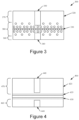
- FIG. 3 illustrates a memory structure 300 having a concentration of doping material positioned within the switching layer in accordance with an embodiment.
- the memory structure 300 includes a switching layer 320 and an oxygen vacancy filament 340 that may correspond to the switching layer 120 and oxygen vacancy filament 140 of FIG. 1 , respectively.
- bottom electrode 110 and top electrode 150 are not shown.
- the memory structure 300 may include a concentration of doping material 330 that corresponds to the doping material 130 of FIG. 1 .
- the switching layer 320 may include a bottom region 360 and a top region 370 .
- the switching layer 320 and the doping material 330 may be disposed using a CVD, ALD, sputtering or other suitable methods.
- thin film layers of switching layer 320 material may be sequentially deposited above a bottom electrode using a gas phase chemical process until the thin film layers reach a determined height that corresponds to the desired position of the layer of doping material 330 within the switching layer 320 , which may form the bottom region 360 of the switching layer 320 .
- multiple gas sources containing different materials may be used at different times of the deposition process to form varying concentrations of the different materials throughout the switching layer 220 .
- the desired position of the layer of doping material 330 may correspond to a gap in the oxygen vacancy filament 340 .
- the desired position of the layer of doping material 330 may be any position located within the switching layer 320 .
- the doping material 330 may be added to the switching layer 320 material and deposited above the bottom region 360 to form a lateral region 380 that includes a varying concentration of the doping material 330 .
- the concentration of the doping material 330 may increase until it reaches a maximum value near the center of the lateral region 380 . Then, the concentration of the doping material 330 may begin to gradually decrease as subsequent layers are deposited above the center of the lateral region 380 . Then, layers of the switching layer 320 material may be deposited that do not include the doping material 330 to form the top region 370 of the switching layer 320 .
- the memory structure 300 may be an RRAM structure and the switching layer 320 may be made of a dielectric material, such as a TMO.
- TMO dielectric material
- TMO's include, but are not limited to, HfOx, TaOx, TiOx or other similar materials.
- the doping material 330 may be Al, Zr, Cd, Gd, Ta, W, Ni, Si, Mg, Sr, Ba, Sc, Y, In, Ge, Sn, Ti, Hf, Nb, Mo, Sb, Te, Tl, Pb, Cu, Ag, composite materials or other similar materials.
- the memory structure 300 may be a CBRAM structure and the switching layer 320 may be made of a solid electrolyte material.
- solid electrolytes include, but are not limited to, YSZ, BASE, LaF 3 , amorphous silicon, GeS 2 or other similar materials.
- the doping material 330 may be Titanium Oxide, Sb, GeS 2 or other similar materials.
- FIG. 4 illustrates a memory structure 400 having multiple doping layers positioned within the switching layer in accordance with an embodiment.
- the memory structure 400 includes a switching layer 420 and an oxygen vacancy filament 440 that may correspond to the switching layer 120 and oxygen vacancy filament 140 of FIG. 1 , respectively.
- bottom electrode 110 and top electrode 150 are not shown.
- the switching layer 420 may include a first doping layer 430 , a second doping layer 435 , a bottom region 460 and a top region 470 .
- the switching layer 420 , the first doping layer 430 and the second doping layer 435 may be disposed using a CVD, ALD, sputtering or other suitable methods.
- Thin film layers of switching layer 420 material may be sequentially deposited above a bottom electrode using a gas phase chemical process until the thin film layers reach a determined height that corresponds to the desired position of the first doping layer 430 within the switching layer 420 , which may form the bottom region 460 of the switching layer 420 .
- the desired position of the first doping layer 430 may correspond to a gap in the oxygen vacancy filament 440 .
- the desired position of the first doping layer 430 may be any position located within the switching layer 420 .
- one or more thin film layers of the doping material may be sequentially deposited to form the first doping layer 430 .
- the memory structure 400 may be an RRAM structure and the switching layer 420 may be made of a dielectric material, such as a TMO.
- TMO dielectric material
- examples of TMO's include, but are not limited to, HfOx, TaOx, TiOx or other similar materials.
- the material of the first doping layer 430 may be Al, Zr, Cd, Gd, Ta, W, Ni, Si, Mg, Sr, Ba, Sc, Y, In, Ge, Sn, Ti, Hf, Nb, Mo, Sb, Te, Tl, Pb, Cu, Ag, composite materials or other similar materials.
- the memory structure 400 may be a CBRAM structure and the switching layer 420 may be made of a solid electrolyte material.
- solid electrolytes include, but are not limited to, YSZ, BASE, LaF 3 , amorphous silicon, GeS 2 or other similar materials.
- the material of the first doping layer 430 may be Titanium Oxide, Sb, GeS 2 or other similar materials.
- layers of the switching layer 420 material may be sequentially deposited above the first layer of doping material 430 prior to disposing a second doping layer 435 forming a layer of switching layer 420 material between the first doping layer 430 and the second doping layer 435 .
- the second doping layer 435 may be disposed directly above the first layer of doping material 430 .
- the second layer of doping material 435 may be disposed using a CVD, ALD, sputtering or other suitable methods.
- the material of the second doping layer 435 may be the same as the material of the first doping layer 430 .
- the material of the second doping layer 435 may be any suitable material that is different than the material of the first doping layer 430 .
- switching layer 420 material may be disposed above the second doping layer 435 to form the top region 470 of the switching layer 420 .
- the doping material of the first doping layer 430 and the doping material of the second doping layer 435 may diffuse to adjacent layers of the switching layer 420 . This may result in the switching layer 420 material between the first doping layer 430 and the second doping layer 435 having concentrations of the doping material of the first doping layer 430 and the doping material of the second doping layer 435 .
- memory structure 400 is illustrated as having multiple doping layers, in other embodiments memory structure may have multiple lateral regions containing varying concentrations of one or more doping materials, as described in FIG. 3 . Furthermore, although memory structure 400 is illustrated as having a first doping layer 430 and a second doping layer 435 , in other embodiments the memory structure 400 may include any number of doping layers located within switching layer 420 .
- FIG. 5 is a flow diagram of a fabrication process for the manufacture of a memory structure in accordance with an embodiment. It may be noted that elements of FIGS. 1 - 4 may be described below to help illustrate method 500 . Method 500 may be performed as one or more operations. It may be noted that method 500 may be performed in any order and may include the same, more or fewer operations. It may be noted that method 500 may be performed by one or more pieces of semiconductor fabrication equipment or fabrication tools.
- Method 500 begins at block 510 by disposing a bottom region of a switching layer above a bottom electrode.
- the switching layer may be disposed by CVD, ALD, sputtering or other suitable methods.
- the switching layer may be a dielectric material such as HfOx, TaOx, TiOx or any suitable material.
- the switching layer may be a solid electrolyte such as YSZ, BASE, LaF 3 or other similar materials.
- a one or more lateral regions including doping material may be disposed above the bottom region.
- the lateral regions may be disposed by CVD, ALD, sputtering or other suitable methods.
- the lateral regions may be one or more doping layers as described in FIGS.
- the lateral regions may be one or more regions having varying concentrations of doping material FIGS. 3 and 4 .
- a top region of the switching layer may be disposed above the lateral regions.
- the top region may be disposed by CVD, ALD, sputtering or any suitable process.
- one layer deposited above or over or under another layer may be directly in contact with the other layer or may have one or more intervening layers.
- one layer deposited between two layers may be directly in contact with the two layers or may have one or more intervening layers.
- a first layer “on” a second layer is in direct contact with that second layer.
- one feature deposited between two features may be in direct contact with the adjacent features or may have one or more intervening layers.
- example or “exemplary” are used herein to mean serving as an example, instance, or illustration. Any aspect or design described herein as “example’ or “exemplary” is not necessarily to be construed as preferred or advantageous over other aspects or designs. Rather, use of the words “example” or “exemplary” is intended to present concepts in a concrete fashion.
- the term “or” is intended to mean an inclusive “or” rather than an exclusive “or.” That is, unless specified otherwise, or clear from context, “X includes A or B” is intended to mean any of the natural inclusive permutations.
Landscapes
- Engineering & Computer Science (AREA)
- Manufacturing & Machinery (AREA)
- Chemical & Material Sciences (AREA)
- Materials Engineering (AREA)
- Semiconductor Memories (AREA)
- Non-Volatile Memory (AREA)
Abstract
Description
Claims (17)
Priority Applications (2)
| Application Number | Priority Date | Filing Date | Title |
|---|---|---|---|
| US17/230,273 US11653580B2 (en) | 2016-11-14 | 2021-04-14 | Non-volatile memory structure with positioned doping |
| US18/114,419 US11963465B2 (en) | 2016-11-14 | 2023-02-27 | Non-volatile memory structure with positioned doping |
Applications Claiming Priority (5)
| Application Number | Priority Date | Filing Date | Title |
|---|---|---|---|
| US201662421774P | 2016-11-14 | 2016-11-14 | |
| US201762503848P | 2017-05-09 | 2017-05-09 | |
| PCT/US2017/061394 WO2018089937A1 (en) | 2016-11-14 | 2017-11-13 | Non-volatile memory structure with positioned doping |
| US201916349252A | 2019-05-10 | 2019-05-10 | |
| US17/230,273 US11653580B2 (en) | 2016-11-14 | 2021-04-14 | Non-volatile memory structure with positioned doping |
Related Parent Applications (2)
| Application Number | Title | Priority Date | Filing Date |
|---|---|---|---|
| US16/349,252 Continuation US11018295B2 (en) | 2016-11-14 | 2017-11-13 | Non-volatile memory structure with positioned doping |
| PCT/US2017/061394 Continuation WO2018089937A1 (en) | 2016-11-14 | 2017-11-13 | Non-volatile memory structure with positioned doping |
Related Child Applications (1)
| Application Number | Title | Priority Date | Filing Date |
|---|---|---|---|
| US18/114,419 Continuation US11963465B2 (en) | 2016-11-14 | 2023-02-27 | Non-volatile memory structure with positioned doping |
Publications (2)
| Publication Number | Publication Date |
|---|---|
| US20210234093A1 US20210234093A1 (en) | 2021-07-29 |
| US11653580B2 true US11653580B2 (en) | 2023-05-16 |
Family
ID=62110041
Family Applications (3)
| Application Number | Title | Priority Date | Filing Date |
|---|---|---|---|
| US16/349,252 Active 2038-01-07 US11018295B2 (en) | 2016-11-14 | 2017-11-13 | Non-volatile memory structure with positioned doping |
| US17/230,273 Active 2037-12-10 US11653580B2 (en) | 2016-11-14 | 2021-04-14 | Non-volatile memory structure with positioned doping |
| US18/114,419 Active US11963465B2 (en) | 2016-11-14 | 2023-02-27 | Non-volatile memory structure with positioned doping |
Family Applications Before (1)
| Application Number | Title | Priority Date | Filing Date |
|---|---|---|---|
| US16/349,252 Active 2038-01-07 US11018295B2 (en) | 2016-11-14 | 2017-11-13 | Non-volatile memory structure with positioned doping |
Family Applications After (1)
| Application Number | Title | Priority Date | Filing Date |
|---|---|---|---|
| US18/114,419 Active US11963465B2 (en) | 2016-11-14 | 2023-02-27 | Non-volatile memory structure with positioned doping |
Country Status (3)
| Country | Link |
|---|---|
| US (3) | US11018295B2 (en) |
| CN (3) | CN116782666A (en) |
| WO (1) | WO2018089937A1 (en) |
Cited By (1)
| Publication number | Priority date | Publication date | Assignee | Title |
|---|---|---|---|---|
| US20230225227A1 (en) * | 2016-11-14 | 2023-07-13 | Hefei Reliance Memory Limited | Non-volatile memory structure with positioned doping |
Families Citing this family (2)
| Publication number | Priority date | Publication date | Assignee | Title |
|---|---|---|---|---|
| CN110148668B (en) * | 2019-05-31 | 2022-05-17 | 中国科学院上海微系统与信息技术研究所 | Al-Sc-Sb-Te phase-change material, phase-change memory unit and preparation method thereof |
| US11615843B2 (en) | 2020-12-17 | 2023-03-28 | International Business Machines Corporation | Controlling voltage resistance through metal-oxide device |
Citations (36)
| Publication number | Priority date | Publication date | Assignee | Title |
|---|---|---|---|---|
| WO2001004949A1 (en) | 1999-07-13 | 2001-01-18 | Advanced Micro Devices, Inc. | Nand type flash memory device |
| US20060097288A1 (en) | 2004-11-10 | 2006-05-11 | Samsung Electronics Co., Ltd. | Cross-point nonvolatile memory devices using binary metal oxide layer as data storage material layer and methods of fabricating the same |
| CN101425559A (en) | 2008-12-05 | 2009-05-06 | 中国科学院微电子研究所 | Resistor conversion type memory and producing method thereof |
| US20090289251A1 (en) | 2008-05-22 | 2009-11-26 | Masahiro Kiyotoshi | Nonvolatile memory device and method for manufacturing same |
| US20100243983A1 (en) | 2009-03-31 | 2010-09-30 | Tony Chiang | Controlled localized defect paths for resistive memories |
| CN101882628A (en) | 2009-05-06 | 2010-11-10 | 中国科学院微电子研究所 | Rectifying device for cross array structure memory |
| CN102683583A (en) | 2011-03-15 | 2012-09-19 | 北京大学 | Unipolar resistive random access memory and manufacturing method thereof |
| WO2013028376A2 (en) | 2011-08-24 | 2013-02-28 | Rambus Inc. | Resistive ram device having improved switching characteristics |
| CN103117359A (en) | 2013-02-07 | 2013-05-22 | 北京大学 | High-reliability nonvolatile memory and preparation method thereof |
| JP2013125903A (en) | 2011-12-15 | 2013-06-24 | Toshiba Corp | Resistance change element |
| US20130294145A1 (en) * | 2012-05-07 | 2013-11-07 | Micron Technology, Inc. | Switching device structures and methods |
| US8866122B1 (en) * | 2012-06-14 | 2014-10-21 | Adesto Technologies Corporation | Resistive switching devices having a buffer layer and methods of formation thereof |
| US20140322862A1 (en) | 2013-04-29 | 2014-10-30 | Asm Ip Holding B.V. | Method of making a resistive random access memory device with metal-doped resistive switching layer |
| CN104183633A (en) | 2013-05-23 | 2014-12-03 | 华邦电子股份有限公司 | Charge storage structure, manufacturing method thereof and nonvolatile memory structure |
| EP2955717A1 (en) * | 2014-06-11 | 2015-12-16 | Commissariat A L'energie Atomique Et Aux Energies Alternatives | Resistive random access memory device |
| EP2955718A1 (en) * | 2014-06-12 | 2015-12-16 | Commissariat A L'energie Atomique Et Aux Energies Alternatives | Resistive random access memory device |
| CN105206743A (en) | 2014-05-28 | 2015-12-30 | 台湾积体电路制造股份有限公司 | Resistive Random-Access Memory (Rram) With Multi-Layer Device Structure |
| US20160379710A1 (en) * | 2013-12-06 | 2016-12-29 | Rambus Inc. | 2t-1r architecture for resistive ram |
| US20170186948A1 (en) * | 2015-12-29 | 2017-06-29 | SK Hynix Inc. | Method for fabricating semiconductor device and method for operating the same |
| US20170186812A1 (en) * | 2015-12-29 | 2017-06-29 | SK Hynix Inc. | Threshold switching device, method for fabricating the same and electronic device including the same |
| US20170213958A1 (en) * | 2016-01-27 | 2017-07-27 | SK Hynix Inc. | Switching device, method of fabricating the same, and resistive random access memory including the switching device as a selection device |
| US20170294580A1 (en) * | 2016-04-08 | 2017-10-12 | Commissariat A L'energie Atomique Et Aux Energies Alternatives | Resistive random access memory, associated manufacturing and programming methods |
| WO2018063287A1 (en) * | 2016-09-30 | 2018-04-05 | Intel Corporation | Conductive bridge resistive random access memory cell |
| WO2018089936A1 (en) * | 2016-11-14 | 2018-05-17 | Rambus Inc. | Rram process intergration scheme and cell structure with reduced masking operations |
| WO2018089937A1 (en) | 2016-11-14 | 2018-05-17 | Rambus Inc. | Non-volatile memory structure with positioned doping |
| US10186553B2 (en) * | 2011-09-30 | 2019-01-22 | Hefei Reliance Memory Limited | Multi-layered conductive metal oxide structures and methods for facilitating enhanced performance characteristics of two-terminal memory cells |
| US10224480B2 (en) * | 2004-02-06 | 2019-03-05 | Hefei Reliance Memory Limited | Two-terminal reversibly switchable memory device |
| WO2019055052A1 (en) * | 2017-09-18 | 2019-03-21 | Intel Corporation | Rram devices with reduced forming voltage |
| US10340312B2 (en) * | 2004-02-06 | 2019-07-02 | Hefei Reliance Memory Limited | Memory element with a reactive metal layer |
| US10388372B2 (en) * | 2014-09-15 | 2019-08-20 | Hefei Reliance Memory Limited | 1T-1R architecture for resistive random access memory |
| US20190259945A1 (en) * | 2018-02-20 | 2019-08-22 | Hankuk University Of Foreign Studies Research Business Foundation | Variable resistor, non-volatile memory element using the same, and method of fabricating the same |
| US20190371399A1 (en) * | 2017-01-20 | 2019-12-05 | Hefei Reliance Memory Limited | Rram write |
| US20190392897A1 (en) * | 2016-09-21 | 2019-12-26 | Hefei Reliance Memory Limited | Techniques for initializing resistive memory devices |
| US20200343306A1 (en) * | 2019-04-26 | 2020-10-29 | Tetramem Inc. | Rram-based crossbar array circuits |
| US10868246B2 (en) * | 2016-09-30 | 2020-12-15 | Intel Corporation | Conductive bridge random access memory (CBRAM) devices with low thermal conductivity electrolyte sublayer |
| US11081168B2 (en) * | 2019-05-23 | 2021-08-03 | Hefei Reliance Memory Limited | Mixed digital-analog memory devices and circuits for secure storage and computing |
-
2017
- 2017-11-13 US US16/349,252 patent/US11018295B2/en active Active
- 2017-11-13 CN CN202310810901.6A patent/CN116782666A/en active Pending
- 2017-11-13 WO PCT/US2017/061394 patent/WO2018089937A1/en active Application Filing
- 2017-11-13 CN CN201780080884.8A patent/CN110114894B/en active Active
- 2017-11-13 CN CN202310810904.XA patent/CN116847662A/en active Pending
-
2021
- 2021-04-14 US US17/230,273 patent/US11653580B2/en active Active
-
2023
- 2023-02-27 US US18/114,419 patent/US11963465B2/en active Active
Patent Citations (62)
| Publication number | Priority date | Publication date | Assignee | Title |
|---|---|---|---|---|
| WO2001004949A1 (en) | 1999-07-13 | 2001-01-18 | Advanced Micro Devices, Inc. | Nand type flash memory device |
| US6235586B1 (en) | 1999-07-13 | 2001-05-22 | Advanced Micro Devices, Inc. | Thin floating gate and conductive select gate in situ doped amorphous silicon material for NAND type flash memory device applications |
| US10340312B2 (en) * | 2004-02-06 | 2019-07-02 | Hefei Reliance Memory Limited | Memory element with a reactive metal layer |
| US10224480B2 (en) * | 2004-02-06 | 2019-03-05 | Hefei Reliance Memory Limited | Two-terminal reversibly switchable memory device |
| US20060097288A1 (en) | 2004-11-10 | 2006-05-11 | Samsung Electronics Co., Ltd. | Cross-point nonvolatile memory devices using binary metal oxide layer as data storage material layer and methods of fabricating the same |
| US20090289251A1 (en) | 2008-05-22 | 2009-11-26 | Masahiro Kiyotoshi | Nonvolatile memory device and method for manufacturing same |
| CN101425559A (en) | 2008-12-05 | 2009-05-06 | 中国科学院微电子研究所 | Resistor conversion type memory and producing method thereof |
| US20100243983A1 (en) | 2009-03-31 | 2010-09-30 | Tony Chiang | Controlled localized defect paths for resistive memories |
| CN101882628A (en) | 2009-05-06 | 2010-11-10 | 中国科学院微电子研究所 | Rectifying device for cross array structure memory |
| CN102683583A (en) | 2011-03-15 | 2012-09-19 | 北京大学 | Unipolar resistive random access memory and manufacturing method thereof |
| WO2013028376A2 (en) | 2011-08-24 | 2013-02-28 | Rambus Inc. | Resistive ram device having improved switching characteristics |
| US10186553B2 (en) * | 2011-09-30 | 2019-01-22 | Hefei Reliance Memory Limited | Multi-layered conductive metal oxide structures and methods for facilitating enhanced performance characteristics of two-terminal memory cells |
| JP2013125903A (en) | 2011-12-15 | 2013-06-24 | Toshiba Corp | Resistance change element |
| US20130294145A1 (en) * | 2012-05-07 | 2013-11-07 | Micron Technology, Inc. | Switching device structures and methods |
| US8866122B1 (en) * | 2012-06-14 | 2014-10-21 | Adesto Technologies Corporation | Resistive switching devices having a buffer layer and methods of formation thereof |
| CN103117359A (en) | 2013-02-07 | 2013-05-22 | 北京大学 | High-reliability nonvolatile memory and preparation method thereof |
| US9379322B2 (en) | 2013-02-07 | 2016-06-28 | Peking University | Highly reliable nonvolatile memory and manufacturing method thereof |
| US20140322862A1 (en) | 2013-04-29 | 2014-10-30 | Asm Ip Holding B.V. | Method of making a resistive random access memory device with metal-doped resistive switching layer |
| CN104183633A (en) | 2013-05-23 | 2014-12-03 | 华邦电子股份有限公司 | Charge storage structure, manufacturing method thereof and nonvolatile memory structure |
| US20160379710A1 (en) * | 2013-12-06 | 2016-12-29 | Rambus Inc. | 2t-1r architecture for resistive ram |
| US10622062B2 (en) * | 2013-12-06 | 2020-04-14 | Hefei Reliance Memory Limited | 2T-1R architecture for resistive ram |
| US20190156886A1 (en) * | 2013-12-06 | 2019-05-23 | Hefei Reliance Memory Limited | 2t-1r architecture for resistive ram |
| US20200211644A1 (en) * | 2013-12-06 | 2020-07-02 | Hefei Reliance Memory Limited | 2t-1r architecture for resistive ram |
| US10199098B2 (en) * | 2013-12-06 | 2019-02-05 | Hefei Reliance Memory Limited | 2T-1R architecture for resistive RAM |
| US10037801B2 (en) * | 2013-12-06 | 2018-07-31 | Hefei Reliance Memory Limited | 2T-1R architecture for resistive RAM |
| US20180330782A1 (en) * | 2013-12-06 | 2018-11-15 | Hefei Reliance Memory Limited | 2t-1r architecture for resistive ram |
| US9281475B2 (en) | 2014-05-28 | 2016-03-08 | Taiwan Semiconductor Manufacturing Company Limited | Resistive random-access memory (RRAM) with multi-layer device structure |
| CN105206743A (en) | 2014-05-28 | 2015-12-30 | 台湾积体电路制造股份有限公司 | Resistive Random-Access Memory (Rram) With Multi-Layer Device Structure |
| EP2955717A1 (en) * | 2014-06-11 | 2015-12-16 | Commissariat A L'energie Atomique Et Aux Energies Alternatives | Resistive random access memory device |
| US20150364679A1 (en) * | 2014-06-11 | 2015-12-17 | Commissariat A L'energie Atomique Et Aux Energies Alternatives | Resistive random access memory device |
| US9722177B2 (en) * | 2014-06-11 | 2017-08-01 | Commissariat à l'énergie atomique et aux énergies alternatives | Resistive random access memory device with a solid electrolyte including a region made of a first metal oxide and doped by a second element distinct from the first metal |
| EP2955718A1 (en) * | 2014-06-12 | 2015-12-16 | Commissariat A L'energie Atomique Et Aux Energies Alternatives | Resistive random access memory device |
| US10388372B2 (en) * | 2014-09-15 | 2019-08-20 | Hefei Reliance Memory Limited | 1T-1R architecture for resistive random access memory |
| US10783964B2 (en) * | 2014-09-15 | 2020-09-22 | Hefei Reliance Memory Limited | 1T-1R architecture for resistive random access memory |
| US20190355414A1 (en) * | 2014-09-15 | 2019-11-21 | Hefei Reliance Memory Limited | 1t-1r architecture for resistive random access memory |
| US20170186812A1 (en) * | 2015-12-29 | 2017-06-29 | SK Hynix Inc. | Threshold switching device, method for fabricating the same and electronic device including the same |
| US20170186948A1 (en) * | 2015-12-29 | 2017-06-29 | SK Hynix Inc. | Method for fabricating semiconductor device and method for operating the same |
| US20170213958A1 (en) * | 2016-01-27 | 2017-07-27 | SK Hynix Inc. | Switching device, method of fabricating the same, and resistive random access memory including the switching device as a selection device |
| US20170294580A1 (en) * | 2016-04-08 | 2017-10-12 | Commissariat A L'energie Atomique Et Aux Energies Alternatives | Resistive random access memory, associated manufacturing and programming methods |
| US11468947B2 (en) * | 2016-09-21 | 2022-10-11 | Hefei Reliance Memory Limited | Techniques for initializing resistive memory devices by applying voltages with different polarities |
| US20210110870A1 (en) * | 2016-09-21 | 2021-04-15 | Hefei Reliance Memory Limited | Techniques for initializing resistive memory devices by applying different polarity voltages across resistance change material |
| US10943655B2 (en) * | 2016-09-21 | 2021-03-09 | Hefei Reliance Memory Limited | Techniques for initializing resistive memory devices by applying different polarity voltages across resistance change material |
| US20190392897A1 (en) * | 2016-09-21 | 2019-12-26 | Hefei Reliance Memory Limited | Techniques for initializing resistive memory devices |
| US10868246B2 (en) * | 2016-09-30 | 2020-12-15 | Intel Corporation | Conductive bridge random access memory (CBRAM) devices with low thermal conductivity electrolyte sublayer |
| WO2018063287A1 (en) * | 2016-09-30 | 2018-04-05 | Intel Corporation | Conductive bridge resistive random access memory cell |
| EP3539132A1 (en) * | 2016-11-14 | 2019-09-18 | Hefei Reliance Memory Limited | Rram process intergration scheme and cell structure with reduced masking operations |
| US20210234093A1 (en) * | 2016-11-14 | 2021-07-29 | Hefei Reliance Memory Limited | Non-volatile memory structure with positioned doping |
| US20190288195A1 (en) * | 2016-11-14 | 2019-09-19 | Hefei Reliance Memory Limited | Non-volatile memory structure with positioned doping |
| WO2018089936A9 (en) | 2016-11-14 | 2019-01-03 | Hefei Reliance Memory Limited | Rram process intergration scheme and cell structure with reduced masking operations |
| US20190288037A1 (en) * | 2016-11-14 | 2019-09-19 | Hefei Reliance Memory Limited | Rram process integration scheme and cell structure with reduced masking operations |
| US10777608B2 (en) * | 2016-11-14 | 2020-09-15 | Hefei Reliance Memory Limited | RRAM process integration scheme and cell structure with reduced masking operations |
| WO2018089936A1 (en) * | 2016-11-14 | 2018-05-17 | Rambus Inc. | Rram process intergration scheme and cell structure with reduced masking operations |
| WO2018089937A1 (en) | 2016-11-14 | 2018-05-17 | Rambus Inc. | Non-volatile memory structure with positioned doping |
| US11018295B2 (en) * | 2016-11-14 | 2021-05-25 | Hefei Reliance Memory Limited | Non-volatile memory structure with positioned doping |
| CN110114894A (en) * | 2016-11-14 | 2019-08-09 | 合肥睿科微电子有限公司 | Using the non-volatile memories structure of positioning doping |
| US10998044B2 (en) * | 2017-01-20 | 2021-05-04 | Hefei Reliance Memory Limited | RRAM write using a ramp control circuit |
| US20190371399A1 (en) * | 2017-01-20 | 2019-12-05 | Hefei Reliance Memory Limited | Rram write |
| WO2019055052A1 (en) * | 2017-09-18 | 2019-03-21 | Intel Corporation | Rram devices with reduced forming voltage |
| US11342499B2 (en) * | 2017-09-18 | 2022-05-24 | Intel Corporation | RRAM devices with reduced forming voltage |
| US20190259945A1 (en) * | 2018-02-20 | 2019-08-22 | Hankuk University Of Foreign Studies Research Business Foundation | Variable resistor, non-volatile memory element using the same, and method of fabricating the same |
| US20200343306A1 (en) * | 2019-04-26 | 2020-10-29 | Tetramem Inc. | Rram-based crossbar array circuits |
| US11081168B2 (en) * | 2019-05-23 | 2021-08-03 | Hefei Reliance Memory Limited | Mixed digital-analog memory devices and circuits for secure storage and computing |
Non-Patent Citations (4)
| Title |
|---|
| First Office Action dated Oct. 17, 2022, issued in related Chinese Application No. 201780080884.8, with English machine translation (14 pages). |
| First Search dated Oct. 9, 2022, issued in related Chinese Application No. 201780080884.8 (2 pages). |
| PCT International Preliminary Reporton Patentability dated May 23, 2019, issued in related International Application No. PCT/US2017/061394 (7 pages). |
| PCT International Search Report and the Written Opinion dated Feb. 20, 2018, issued in related International Application No. PCT/US2017/061394 (8 pages). |
Cited By (2)
| Publication number | Priority date | Publication date | Assignee | Title |
|---|---|---|---|---|
| US20230225227A1 (en) * | 2016-11-14 | 2023-07-13 | Hefei Reliance Memory Limited | Non-volatile memory structure with positioned doping |
| US11963465B2 (en) * | 2016-11-14 | 2024-04-16 | Hefei Reliance Memory Limited | Non-volatile memory structure with positioned doping |
Also Published As
| Publication number | Publication date |
|---|---|
| CN116847662A (en) | 2023-10-03 |
| WO2018089937A1 (en) | 2018-05-17 |
| CN116782666A (en) | 2023-09-19 |
| US11018295B2 (en) | 2021-05-25 |
| US20190288195A1 (en) | 2019-09-19 |
| US20210234093A1 (en) | 2021-07-29 |
| CN110114894B (en) | 2023-07-28 |
| CN110114894A (en) | 2019-08-09 |
| US20230225227A1 (en) | 2023-07-13 |
| US11963465B2 (en) | 2024-04-16 |
Similar Documents
| Publication | Publication Date | Title |
|---|---|---|
| US11653580B2 (en) | Non-volatile memory structure with positioned doping | |
| US9553264B2 (en) | Memory cells and semiconductor structures including electrodes comprising a metal, and related methods | |
| US8847192B2 (en) | Resistive switching devices having alloyed electrodes and methods of formation thereof | |
| US8263420B2 (en) | Optimized electrodes for Re-RAM | |
| US9331276B2 (en) | Nonvolatile resistive memory element with an oxygen-gettering layer | |
| KR101522439B1 (en) | Non-volatile resistive-switching memories | |
| US7602042B2 (en) | Nonvolatile memory device, array of nonvolatile memory devices, and methods of making the same | |
| US20190157348A1 (en) | Multi-layered conductive metal oxide structures and methods for facilitating enhanced performance characteristics of two-terminal memory cells | |
| US20120217461A1 (en) | Semiconductor memory device and method of manufacturing the same | |
| US20220406845A1 (en) | Rram process integration scheme and cell structure with reduced masking operations | |
| US8866122B1 (en) | Resistive switching devices having a buffer layer and methods of formation thereof | |
| US9917250B2 (en) | Switching device, method of fabricating the same, and resistive random access memory including the switching device as a selection device | |
| EP3046155B1 (en) | Conductive bridging memory device with cation supply electrode comprising cu-si-te |
Legal Events
| Date | Code | Title | Description |
|---|---|---|---|
| AS | Assignment |
Owner name: HEFEI RELIANCE MEMORY LIMITED, CHINA Free format text: ASSIGNMENT OF ASSIGNORS INTEREST;ASSIGNOR:RAMBUS INC.;REEL/FRAME:055929/0492 Effective date: 20180504 Owner name: RAMBUS INC., CALIFORNIA Free format text: ASSIGNMENT OF ASSIGNORS INTEREST;ASSIGNORS:LU, ZHICHAO;BRONNER, GARY;REEL/FRAME:055916/0864 Effective date: 20170306 |
|
| FEPP | Fee payment procedure |
Free format text: ENTITY STATUS SET TO UNDISCOUNTED (ORIGINAL EVENT CODE: BIG.); ENTITY STATUS OF PATENT OWNER: LARGE ENTITY |
|
| STPP | Information on status: patent application and granting procedure in general |
Free format text: APPLICATION DISPATCHED FROM PREEXAM, NOT YET DOCKETED |
|
| STPP | Information on status: patent application and granting procedure in general |
Free format text: DOCKETED NEW CASE - READY FOR EXAMINATION |
|
| STPP | Information on status: patent application and granting procedure in general |
Free format text: NON FINAL ACTION MAILED |
|
| STPP | Information on status: patent application and granting procedure in general |
Free format text: FINAL REJECTION MAILED |
|
| STPP | Information on status: patent application and granting procedure in general |
Free format text: RESPONSE AFTER FINAL ACTION FORWARDED TO EXAMINER |
|
| STCF | Information on status: patent grant |
Free format text: PATENTED CASE |