US11626337B2 - Semiconductor devices and methods of manufacturing semiconductor devices - Google Patents
Semiconductor devices and methods of manufacturing semiconductor devices Download PDFInfo
- Publication number
- US11626337B2 US11626337B2 US16/877,652 US202016877652A US11626337B2 US 11626337 B2 US11626337 B2 US 11626337B2 US 202016877652 A US202016877652 A US 202016877652A US 11626337 B2 US11626337 B2 US 11626337B2
- Authority
- US
- United States
- Prior art keywords
- module
- component
- main
- encapsulant
- substrate
- Prior art date
- Legal status (The legal status is an assumption and is not a legal conclusion. Google has not performed a legal analysis and makes no representation as to the accuracy of the status listed.)
- Active, expires
Links
- 239000004065 semiconductor Substances 0.000 title claims abstract description 87
- 238000000034 method Methods 0.000 title abstract description 53
- 238000004519 manufacturing process Methods 0.000 title description 26
- 239000000758 substrate Substances 0.000 claims abstract description 170
- 239000008393 encapsulating agent Substances 0.000 claims abstract description 108
- 239000010410 layer Substances 0.000 description 53
- 230000008569 process Effects 0.000 description 42
- PXHVJJICTQNCMI-UHFFFAOYSA-N Nickel Chemical compound [Ni] PXHVJJICTQNCMI-UHFFFAOYSA-N 0.000 description 15
- KDLHZDBZIXYQEI-UHFFFAOYSA-N Palladium Chemical compound [Pd] KDLHZDBZIXYQEI-UHFFFAOYSA-N 0.000 description 15
- 239000004020 conductor Substances 0.000 description 15
- 239000010936 titanium Substances 0.000 description 15
- 239000010949 copper Substances 0.000 description 14
- 238000005229 chemical vapour deposition Methods 0.000 description 13
- 239000000463 material Substances 0.000 description 12
- RTAQQCXQSZGOHL-UHFFFAOYSA-N Titanium Chemical compound [Ti] RTAQQCXQSZGOHL-UHFFFAOYSA-N 0.000 description 10
- 238000000231 atomic layer deposition Methods 0.000 description 10
- 239000010931 gold Substances 0.000 description 10
- 238000004518 low pressure chemical vapour deposition Methods 0.000 description 10
- 238000005240 physical vapour deposition Methods 0.000 description 10
- 238000000623 plasma-assisted chemical vapour deposition Methods 0.000 description 10
- 229910052719 titanium Inorganic materials 0.000 description 10
- WFKWXMTUELFFGS-UHFFFAOYSA-N tungsten Chemical compound [W] WFKWXMTUELFFGS-UHFFFAOYSA-N 0.000 description 10
- 229910052721 tungsten Inorganic materials 0.000 description 10
- 239000010937 tungsten Substances 0.000 description 10
- 208000032365 Electromagnetic interference Diseases 0.000 description 9
- 239000003989 dielectric material Substances 0.000 description 9
- RYGMFSIKBFXOCR-UHFFFAOYSA-N Copper Chemical compound [Cu] RYGMFSIKBFXOCR-UHFFFAOYSA-N 0.000 description 8
- 229910052802 copper Inorganic materials 0.000 description 8
- 229910052751 metal Inorganic materials 0.000 description 8
- 239000002184 metal Substances 0.000 description 8
- 230000015572 biosynthetic process Effects 0.000 description 7
- 238000009713 electroplating Methods 0.000 description 7
- 229910052709 silver Inorganic materials 0.000 description 7
- 239000004642 Polyimide Substances 0.000 description 6
- BQCADISMDOOEFD-UHFFFAOYSA-N Silver Chemical compound [Ag] BQCADISMDOOEFD-UHFFFAOYSA-N 0.000 description 6
- UMIVXZPTRXBADB-UHFFFAOYSA-N benzocyclobutene Chemical compound C1=CC=C2CCC2=C1 UMIVXZPTRXBADB-UHFFFAOYSA-N 0.000 description 6
- 229920002577 polybenzoxazole Polymers 0.000 description 6
- 229920001721 polyimide Polymers 0.000 description 6
- 229920000642 polymer Polymers 0.000 description 6
- 239000004332 silver Substances 0.000 description 6
- 229910052782 aluminium Inorganic materials 0.000 description 5
- XAGFODPZIPBFFR-UHFFFAOYSA-N aluminium Chemical compound [Al] XAGFODPZIPBFFR-UHFFFAOYSA-N 0.000 description 5
- 239000000945 filler Substances 0.000 description 5
- 239000010408 film Substances 0.000 description 5
- PCHJSUWPFVWCPO-UHFFFAOYSA-N gold Chemical compound [Au] PCHJSUWPFVWCPO-UHFFFAOYSA-N 0.000 description 5
- 229910052737 gold Inorganic materials 0.000 description 5
- 238000000227 grinding Methods 0.000 description 5
- 229910052759 nickel Inorganic materials 0.000 description 5
- 229910052763 palladium Inorganic materials 0.000 description 5
- 229920005989 resin Polymers 0.000 description 5
- 239000011347 resin Substances 0.000 description 5
- JYEUMXHLPRZUAT-UHFFFAOYSA-N 1,2,3-triazine Chemical compound C1=CN=NN=C1 JYEUMXHLPRZUAT-UHFFFAOYSA-N 0.000 description 4
- XQUPVDVFXZDTLT-UHFFFAOYSA-N 1-[4-[[4-(2,5-dioxopyrrol-1-yl)phenyl]methyl]phenyl]pyrrole-2,5-dione Chemical compound O=C1C=CC(=O)N1C(C=C1)=CC=C1CC1=CC=C(N2C(C=CC2=O)=O)C=C1 XQUPVDVFXZDTLT-UHFFFAOYSA-N 0.000 description 4
- 239000004698 Polyethylene Substances 0.000 description 4
- 239000004743 Polypropylene Substances 0.000 description 4
- XUIMIQQOPSSXEZ-UHFFFAOYSA-N Silicon Chemical compound [Si] XUIMIQQOPSSXEZ-UHFFFAOYSA-N 0.000 description 4
- 150000001875 compounds Chemical class 0.000 description 4
- 230000008878 coupling Effects 0.000 description 4
- 238000010168 coupling process Methods 0.000 description 4
- 238000005859 coupling reaction Methods 0.000 description 4
- 238000007772 electroless plating Methods 0.000 description 4
- 239000003822 epoxy resin Substances 0.000 description 4
- 238000010438 heat treatment Methods 0.000 description 4
- 238000003475 lamination Methods 0.000 description 4
- 239000012778 molding material Substances 0.000 description 4
- 238000000465 moulding Methods 0.000 description 4
- 229920003192 poly(bis maleimide) Polymers 0.000 description 4
- 229920000647 polyepoxide Polymers 0.000 description 4
- 229920000573 polyethylene Polymers 0.000 description 4
- -1 polypropylene Polymers 0.000 description 4
- 229920001155 polypropylene Polymers 0.000 description 4
- 238000007639 printing Methods 0.000 description 4
- 229910052710 silicon Inorganic materials 0.000 description 4
- 239000010703 silicon Substances 0.000 description 4
- 229910000679 solder Inorganic materials 0.000 description 4
- 238000004544 sputter deposition Methods 0.000 description 4
- 239000000126 substance Substances 0.000 description 4
- 239000000654 additive Substances 0.000 description 3
- 230000003647 oxidation Effects 0.000 description 3
- 238000007254 oxidation reaction Methods 0.000 description 3
- 238000000059 patterning Methods 0.000 description 3
- 238000005507 spraying Methods 0.000 description 3
- 239000004593 Epoxy Substances 0.000 description 2
- 229910052581 Si3N4 Inorganic materials 0.000 description 2
- VYPSYNLAJGMNEJ-UHFFFAOYSA-N Silicium dioxide Chemical compound O=[Si]=O VYPSYNLAJGMNEJ-UHFFFAOYSA-N 0.000 description 2
- 239000002313 adhesive film Substances 0.000 description 2
- 239000002390 adhesive tape Substances 0.000 description 2
- 238000013459 approach Methods 0.000 description 2
- 238000000748 compression moulding Methods 0.000 description 2
- 239000012792 core layer Substances 0.000 description 2
- 238000005137 deposition process Methods 0.000 description 2
- 239000012777 electrically insulating material Substances 0.000 description 2
- 238000001704 evaporation Methods 0.000 description 2
- 239000011521 glass Substances 0.000 description 2
- 239000011256 inorganic filler Substances 0.000 description 2
- 229910003475 inorganic filler Inorganic materials 0.000 description 2
- 239000010954 inorganic particle Substances 0.000 description 2
- 239000007788 liquid Substances 0.000 description 2
- 239000007791 liquid phase Substances 0.000 description 2
- 239000000203 mixture Substances 0.000 description 2
- 238000002161 passivation Methods 0.000 description 2
- 239000005011 phenolic resin Substances 0.000 description 2
- 238000007747 plating Methods 0.000 description 2
- 229920000058 polyacrylate Polymers 0.000 description 2
- 229920001296 polysiloxane Polymers 0.000 description 2
- KCTAWXVAICEBSD-UHFFFAOYSA-N prop-2-enoyloxy prop-2-eneperoxoate Chemical compound C=CC(=O)OOOC(=O)C=C KCTAWXVAICEBSD-UHFFFAOYSA-N 0.000 description 2
- 230000001681 protective effect Effects 0.000 description 2
- 238000007650 screen-printing Methods 0.000 description 2
- HQVNEWCFYHHQES-UHFFFAOYSA-N silicon nitride Chemical compound N12[Si]34N5[Si]62N3[Si]51N64 HQVNEWCFYHHQES-UHFFFAOYSA-N 0.000 description 2
- 229910052814 silicon oxide Inorganic materials 0.000 description 2
- 229920002050 silicone resin Polymers 0.000 description 2
- 238000005245 sintering Methods 0.000 description 2
- 238000004528 spin coating Methods 0.000 description 2
- 239000010409 thin film Substances 0.000 description 2
- 229910017944 Ag—Cu Inorganic materials 0.000 description 1
- 229910020816 Sn Pb Inorganic materials 0.000 description 1
- 229910020836 Sn-Ag Inorganic materials 0.000 description 1
- 229910020830 Sn-Bi Inorganic materials 0.000 description 1
- 229910020888 Sn-Cu Inorganic materials 0.000 description 1
- 229910020922 Sn-Pb Inorganic materials 0.000 description 1
- 229910020988 Sn—Ag Inorganic materials 0.000 description 1
- 229910018731 Sn—Au Inorganic materials 0.000 description 1
- 229910018728 Sn—Bi Inorganic materials 0.000 description 1
- 229910019204 Sn—Cu Inorganic materials 0.000 description 1
- 229910008783 Sn—Pb Inorganic materials 0.000 description 1
- ATJFFYVFTNAWJD-UHFFFAOYSA-N Tin Chemical compound [Sn] ATJFFYVFTNAWJD-UHFFFAOYSA-N 0.000 description 1
- 230000000996 additive effect Effects 0.000 description 1
- 239000003990 capacitor Substances 0.000 description 1
- 238000010276 construction Methods 0.000 description 1
- 230000003247 decreasing effect Effects 0.000 description 1
- 230000006870 function Effects 0.000 description 1
- 230000005484 gravity Effects 0.000 description 1
- 230000001939 inductive effect Effects 0.000 description 1
- 229910052745 lead Inorganic materials 0.000 description 1
- 238000001465 metallisation Methods 0.000 description 1
- 238000012986 modification Methods 0.000 description 1
- 230000004048 modification Effects 0.000 description 1
- 239000011368 organic material Substances 0.000 description 1
- 239000002245 particle Substances 0.000 description 1
- 238000000206 photolithography Methods 0.000 description 1
- 229920002120 photoresistant polymer Polymers 0.000 description 1
- 230000009467 reduction Effects 0.000 description 1
Images


Classifications
-
- H—ELECTRICITY
- H01—ELECTRIC ELEMENTS
- H01L—SEMICONDUCTOR DEVICES NOT COVERED BY CLASS H10
- H01L23/00—Details of semiconductor or other solid state devices
- H01L23/552—Protection against radiation, e.g. light or electromagnetic waves
-
- H—ELECTRICITY
- H01—ELECTRIC ELEMENTS
- H01L—SEMICONDUCTOR DEVICES NOT COVERED BY CLASS H10
- H01L23/00—Details of semiconductor or other solid state devices
- H01L23/28—Encapsulations, e.g. encapsulating layers, coatings, e.g. for protection
- H01L23/31—Encapsulations, e.g. encapsulating layers, coatings, e.g. for protection characterised by the arrangement or shape
- H01L23/3107—Encapsulations, e.g. encapsulating layers, coatings, e.g. for protection characterised by the arrangement or shape the device being completely enclosed
- H01L23/3121—Encapsulations, e.g. encapsulating layers, coatings, e.g. for protection characterised by the arrangement or shape the device being completely enclosed a substrate forming part of the encapsulation
- H01L23/3128—Encapsulations, e.g. encapsulating layers, coatings, e.g. for protection characterised by the arrangement or shape the device being completely enclosed a substrate forming part of the encapsulation the substrate having spherical bumps for external connection
-
- H—ELECTRICITY
- H01—ELECTRIC ELEMENTS
- H01L—SEMICONDUCTOR DEVICES NOT COVERED BY CLASS H10
- H01L23/00—Details of semiconductor or other solid state devices
- H01L23/28—Encapsulations, e.g. encapsulating layers, coatings, e.g. for protection
- H01L23/31—Encapsulations, e.g. encapsulating layers, coatings, e.g. for protection characterised by the arrangement or shape
-
- H—ELECTRICITY
- H01—ELECTRIC ELEMENTS
- H01L—SEMICONDUCTOR DEVICES NOT COVERED BY CLASS H10
- H01L21/00—Processes or apparatus adapted for the manufacture or treatment of semiconductor or solid state devices or of parts thereof
- H01L21/02—Manufacture or treatment of semiconductor devices or of parts thereof
- H01L21/04—Manufacture or treatment of semiconductor devices or of parts thereof the devices having potential barriers, e.g. a PN junction, depletion layer or carrier concentration layer
- H01L21/50—Assembly of semiconductor devices using processes or apparatus not provided for in a single one of the subgroups H01L21/06 - H01L21/326, e.g. sealing of a cap to a base of a container
- H01L21/56—Encapsulations, e.g. encapsulation layers, coatings
- H01L21/561—Batch processing
-
- H—ELECTRICITY
- H01—ELECTRIC ELEMENTS
- H01L—SEMICONDUCTOR DEVICES NOT COVERED BY CLASS H10
- H01L21/00—Processes or apparatus adapted for the manufacture or treatment of semiconductor or solid state devices or of parts thereof
- H01L21/67—Apparatus specially adapted for handling semiconductor or electric solid state devices during manufacture or treatment thereof; Apparatus specially adapted for handling wafers during manufacture or treatment of semiconductor or electric solid state devices or components ; Apparatus not specifically provided for elsewhere
- H01L21/683—Apparatus specially adapted for handling semiconductor or electric solid state devices during manufacture or treatment thereof; Apparatus specially adapted for handling wafers during manufacture or treatment of semiconductor or electric solid state devices or components ; Apparatus not specifically provided for elsewhere for supporting or gripping
- H01L21/6835—Apparatus specially adapted for handling semiconductor or electric solid state devices during manufacture or treatment thereof; Apparatus specially adapted for handling wafers during manufacture or treatment of semiconductor or electric solid state devices or components ; Apparatus not specifically provided for elsewhere for supporting or gripping using temporarily an auxiliary support
-
- H—ELECTRICITY
- H01—ELECTRIC ELEMENTS
- H01L—SEMICONDUCTOR DEVICES NOT COVERED BY CLASS H10
- H01L21/00—Processes or apparatus adapted for the manufacture or treatment of semiconductor or solid state devices or of parts thereof
- H01L21/70—Manufacture or treatment of devices consisting of a plurality of solid state components formed in or on a common substrate or of parts thereof; Manufacture of integrated circuit devices or of parts thereof
- H01L21/77—Manufacture or treatment of devices consisting of a plurality of solid state components or integrated circuits formed in, or on, a common substrate
- H01L21/78—Manufacture or treatment of devices consisting of a plurality of solid state components or integrated circuits formed in, or on, a common substrate with subsequent division of the substrate into plural individual devices
-
- H—ELECTRICITY
- H01—ELECTRIC ELEMENTS
- H01L—SEMICONDUCTOR DEVICES NOT COVERED BY CLASS H10
- H01L24/00—Arrangements for connecting or disconnecting semiconductor or solid-state bodies; Methods or apparatus related thereto
- H01L24/01—Means for bonding being attached to, or being formed on, the surface to be connected, e.g. chip-to-package, die-attach, "first-level" interconnects; Manufacturing methods related thereto
- H01L24/18—High density interconnect [HDI] connectors; Manufacturing methods related thereto
- H01L24/19—Manufacturing methods of high density interconnect preforms
-
- H—ELECTRICITY
- H01—ELECTRIC ELEMENTS
- H01L—SEMICONDUCTOR DEVICES NOT COVERED BY CLASS H10
- H01L24/00—Arrangements for connecting or disconnecting semiconductor or solid-state bodies; Methods or apparatus related thereto
- H01L24/01—Means for bonding being attached to, or being formed on, the surface to be connected, e.g. chip-to-package, die-attach, "first-level" interconnects; Manufacturing methods related thereto
- H01L24/18—High density interconnect [HDI] connectors; Manufacturing methods related thereto
- H01L24/20—Structure, shape, material or disposition of high density interconnect preforms
-
- H—ELECTRICITY
- H01—ELECTRIC ELEMENTS
- H01L—SEMICONDUCTOR DEVICES NOT COVERED BY CLASS H10
- H01L24/00—Arrangements for connecting or disconnecting semiconductor or solid-state bodies; Methods or apparatus related thereto
- H01L24/93—Batch processes
- H01L24/94—Batch processes at wafer-level, i.e. with connecting carried out on a wafer comprising a plurality of undiced individual devices
-
- H—ELECTRICITY
- H01—ELECTRIC ELEMENTS
- H01L—SEMICONDUCTOR DEVICES NOT COVERED BY CLASS H10
- H01L24/00—Arrangements for connecting or disconnecting semiconductor or solid-state bodies; Methods or apparatus related thereto
- H01L24/93—Batch processes
- H01L24/95—Batch processes at chip-level, i.e. with connecting carried out on a plurality of singulated devices, i.e. on diced chips
- H01L24/96—Batch processes at chip-level, i.e. with connecting carried out on a plurality of singulated devices, i.e. on diced chips the devices being encapsulated in a common layer, e.g. neo-wafer or pseudo-wafer, said common layer being separable into individual assemblies after connecting
-
- H—ELECTRICITY
- H01—ELECTRIC ELEMENTS
- H01L—SEMICONDUCTOR DEVICES NOT COVERED BY CLASS H10
- H01L25/00—Assemblies consisting of a plurality of individual semiconductor or other solid state devices ; Multistep manufacturing processes thereof
- H01L25/03—Assemblies consisting of a plurality of individual semiconductor or other solid state devices ; Multistep manufacturing processes thereof all the devices being of a type provided for in the same subgroup of groups H01L27/00 - H01L33/00, or in a single subclass of H10K, H10N, e.g. assemblies of rectifier diodes
- H01L25/04—Assemblies consisting of a plurality of individual semiconductor or other solid state devices ; Multistep manufacturing processes thereof all the devices being of a type provided for in the same subgroup of groups H01L27/00 - H01L33/00, or in a single subclass of H10K, H10N, e.g. assemblies of rectifier diodes the devices not having separate containers
- H01L25/065—Assemblies consisting of a plurality of individual semiconductor or other solid state devices ; Multistep manufacturing processes thereof all the devices being of a type provided for in the same subgroup of groups H01L27/00 - H01L33/00, or in a single subclass of H10K, H10N, e.g. assemblies of rectifier diodes the devices not having separate containers the devices being of a type provided for in group H01L27/00
- H01L25/0655—Assemblies consisting of a plurality of individual semiconductor or other solid state devices ; Multistep manufacturing processes thereof all the devices being of a type provided for in the same subgroup of groups H01L27/00 - H01L33/00, or in a single subclass of H10K, H10N, e.g. assemblies of rectifier diodes the devices not having separate containers the devices being of a type provided for in group H01L27/00 the devices being arranged next to each other
-
- H—ELECTRICITY
- H01—ELECTRIC ELEMENTS
- H01L—SEMICONDUCTOR DEVICES NOT COVERED BY CLASS H10
- H01L25/00—Assemblies consisting of a plurality of individual semiconductor or other solid state devices ; Multistep manufacturing processes thereof
- H01L25/03—Assemblies consisting of a plurality of individual semiconductor or other solid state devices ; Multistep manufacturing processes thereof all the devices being of a type provided for in the same subgroup of groups H01L27/00 - H01L33/00, or in a single subclass of H10K, H10N, e.g. assemblies of rectifier diodes
- H01L25/10—Assemblies consisting of a plurality of individual semiconductor or other solid state devices ; Multistep manufacturing processes thereof all the devices being of a type provided for in the same subgroup of groups H01L27/00 - H01L33/00, or in a single subclass of H10K, H10N, e.g. assemblies of rectifier diodes the devices having separate containers
- H01L25/105—Assemblies consisting of a plurality of individual semiconductor or other solid state devices ; Multistep manufacturing processes thereof all the devices being of a type provided for in the same subgroup of groups H01L27/00 - H01L33/00, or in a single subclass of H10K, H10N, e.g. assemblies of rectifier diodes the devices having separate containers the devices being of a type provided for in group H01L27/00
-
- H—ELECTRICITY
- H01—ELECTRIC ELEMENTS
- H01L—SEMICONDUCTOR DEVICES NOT COVERED BY CLASS H10
- H01L2221/00—Processes or apparatus adapted for the manufacture or treatment of semiconductor or solid state devices or of parts thereof covered by H01L21/00
- H01L2221/67—Apparatus for handling semiconductor or electric solid state devices during manufacture or treatment thereof; Apparatus for handling wafers during manufacture or treatment of semiconductor or electric solid state devices or components; Apparatus not specifically provided for elsewhere
- H01L2221/683—Apparatus for handling semiconductor or electric solid state devices during manufacture or treatment thereof; Apparatus for handling wafers during manufacture or treatment of semiconductor or electric solid state devices or components; Apparatus not specifically provided for elsewhere for supporting or gripping
- H01L2221/68304—Apparatus for handling semiconductor or electric solid state devices during manufacture or treatment thereof; Apparatus for handling wafers during manufacture or treatment of semiconductor or electric solid state devices or components; Apparatus not specifically provided for elsewhere for supporting or gripping using temporarily an auxiliary support
- H01L2221/68359—Apparatus for handling semiconductor or electric solid state devices during manufacture or treatment thereof; Apparatus for handling wafers during manufacture or treatment of semiconductor or electric solid state devices or components; Apparatus not specifically provided for elsewhere for supporting or gripping using temporarily an auxiliary support used as a support during manufacture of interconnect decals or build up layers
-
- H—ELECTRICITY
- H01—ELECTRIC ELEMENTS
- H01L—SEMICONDUCTOR DEVICES NOT COVERED BY CLASS H10
- H01L2224/00—Indexing scheme for arrangements for connecting or disconnecting semiconductor or solid-state bodies and methods related thereto as covered by H01L24/00
- H01L2224/01—Means for bonding being attached to, or being formed on, the surface to be connected, e.g. chip-to-package, die-attach, "first-level" interconnects; Manufacturing methods related thereto
- H01L2224/02—Bonding areas; Manufacturing methods related thereto
- H01L2224/04—Structure, shape, material or disposition of the bonding areas prior to the connecting process
- H01L2224/04105—Bonding areas formed on an encapsulation of the semiconductor or solid-state body, e.g. bonding areas on chip-scale packages
-
- H—ELECTRICITY
- H01—ELECTRIC ELEMENTS
- H01L—SEMICONDUCTOR DEVICES NOT COVERED BY CLASS H10
- H01L2224/00—Indexing scheme for arrangements for connecting or disconnecting semiconductor or solid-state bodies and methods related thereto as covered by H01L24/00
- H01L2224/01—Means for bonding being attached to, or being formed on, the surface to be connected, e.g. chip-to-package, die-attach, "first-level" interconnects; Manufacturing methods related thereto
- H01L2224/10—Bump connectors; Manufacturing methods related thereto
- H01L2224/12—Structure, shape, material or disposition of the bump connectors prior to the connecting process
- H01L2224/12105—Bump connectors formed on an encapsulation of the semiconductor or solid-state body, e.g. bumps on chip-scale packages
-
- H—ELECTRICITY
- H01—ELECTRIC ELEMENTS
- H01L—SEMICONDUCTOR DEVICES NOT COVERED BY CLASS H10
- H01L2224/00—Indexing scheme for arrangements for connecting or disconnecting semiconductor or solid-state bodies and methods related thereto as covered by H01L24/00
- H01L2224/01—Means for bonding being attached to, or being formed on, the surface to be connected, e.g. chip-to-package, die-attach, "first-level" interconnects; Manufacturing methods related thereto
- H01L2224/18—High density interconnect [HDI] connectors; Manufacturing methods related thereto
- H01L2224/20—Structure, shape, material or disposition of high density interconnect preforms
- H01L2224/21—Structure, shape, material or disposition of high density interconnect preforms of an individual HDI interconnect
- H01L2224/214—Connecting portions
-
- H—ELECTRICITY
- H01—ELECTRIC ELEMENTS
- H01L—SEMICONDUCTOR DEVICES NOT COVERED BY CLASS H10
- H01L2224/00—Indexing scheme for arrangements for connecting or disconnecting semiconductor or solid-state bodies and methods related thereto as covered by H01L24/00
- H01L2224/01—Means for bonding being attached to, or being formed on, the surface to be connected, e.g. chip-to-package, die-attach, "first-level" interconnects; Manufacturing methods related thereto
- H01L2224/18—High density interconnect [HDI] connectors; Manufacturing methods related thereto
- H01L2224/23—Structure, shape, material or disposition of the high density interconnect connectors after the connecting process
- H01L2224/24—Structure, shape, material or disposition of the high density interconnect connectors after the connecting process of an individual high density interconnect connector
- H01L2224/241—Disposition
- H01L2224/24135—Connecting between different semiconductor or solid-state bodies, i.e. chip-to-chip
- H01L2224/24137—Connecting between different semiconductor or solid-state bodies, i.e. chip-to-chip the bodies being arranged next to each other, e.g. on a common substrate
-
- H—ELECTRICITY
- H01—ELECTRIC ELEMENTS
- H01L—SEMICONDUCTOR DEVICES NOT COVERED BY CLASS H10
- H01L2224/00—Indexing scheme for arrangements for connecting or disconnecting semiconductor or solid-state bodies and methods related thereto as covered by H01L24/00
- H01L2224/93—Batch processes
- H01L2224/95—Batch processes at chip-level, i.e. with connecting carried out on a plurality of singulated devices, i.e. on diced chips
- H01L2224/96—Batch processes at chip-level, i.e. with connecting carried out on a plurality of singulated devices, i.e. on diced chips the devices being encapsulated in a common layer, e.g. neo-wafer or pseudo-wafer, said common layer being separable into individual assemblies after connecting
-
- H—ELECTRICITY
- H01—ELECTRIC ELEMENTS
- H01L—SEMICONDUCTOR DEVICES NOT COVERED BY CLASS H10
- H01L2924/00—Indexing scheme for arrangements or methods for connecting or disconnecting semiconductor or solid-state bodies as covered by H01L24/00
- H01L2924/30—Technical effects
- H01L2924/301—Electrical effects
- H01L2924/3025—Electromagnetic shielding
-
- H—ELECTRICITY
- H01—ELECTRIC ELEMENTS
- H01L—SEMICONDUCTOR DEVICES NOT COVERED BY CLASS H10
- H01L2924/00—Indexing scheme for arrangements or methods for connecting or disconnecting semiconductor or solid-state bodies as covered by H01L24/00
- H01L2924/30—Technical effects
- H01L2924/35—Mechanical effects
- H01L2924/351—Thermal stress
- H01L2924/3511—Warping
Definitions
- the present disclosure relates, in general, to electronic devices, and more particularly, to semiconductor devices and methods for manufacturing semiconductor devices.
- FIG. 1 shows a cross-sectional view of an example semiconductor device.
- FIGS. 2 A to 2 I show cross-sectional views of an example method for manufacturing an example semiconductor device.
- FIG. 3 shows a cross-sectional view of an example semiconductor device.
- FIGS. 4 A to 4 I show cross-sectional views of an example method for manufacturing an example semiconductor device.
- x or y means any element of the three-element set ⁇ (x), (y), (x, y) ⁇ .
- x, y, or z means any element of the seven-element set ⁇ (x), (y), (z), (x, y), (x, z), z), (x, y, z) ⁇ .
- Coupled may be used to describe two elements directly contacting each other or describe two elements indirectly connected by one or more other elements.
- element A is coupled to element B, then element A can be directly contacting element B or indirectly connected to element B by an intervening element C.
- the terms “over” or “on” may be used to describe two elements directly contacting each other or describe two elements indirectly connected by one or more other elements.
- a semiconductor device comprises a main substrate comprising a first side and a main conductive structure, and a first component module over the first side of the main substrate.
- the first component module comprises a first electronic component and a first module encapsulant contacting a lateral side of the first electronic component.
- the semiconductor device further comprises a second component module over the first side of the main substrate.
- the second component module comprises a second electronic component and a second module encapsulant contacting a lateral side of the second electronic component.
- the semiconductor device further comprises a main encapsulant over the first side of the main substrate and between the first component module and the second component module
- a method of manufacturing a semiconductor device comprises providing a main substrate comprising a first side and a main conductive structure, providing a first component module over the first side of the main substrate, the first component module comprising a first electronic component and a first module encapsulant contacting a lateral side of the first electronic component, providing a second component module over the first side of the main substrate, the second component module comprising a second electronic component, and a second module encapsulant contacting a lateral side of the second electronic component, and encapsulating the first side of the main substrate and lateral sides of the first and second component modules with a main encapsulant.
- a method of manufacturing a semiconductor device comprises providing a plurality of electronic components in a module encapsulant, wherein component terminals of the electronic components are exposed external to the module encapsulant, providing a module substrate over the electronic components, wherein a module conductive structure of the module substrate is coupled with the component terminals, singulating the module encapsulant to provide a plurality of component modules, providing the component modules on a carrier, providing a main encapsulant over the carrier and contacting lateral sides of the component modules, removing the carrier, providing a main substrate over the main encapsulant, and singulating the main encapsulant to provide a semiconductor device comprising two component modules.
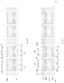
- FIG. 1 shows a cross-sectional view of an example semiconductor device.
- semiconductor device 100 can comprise main substrate 110 , component module 120 , component module 130 , vertical interconnects 140 , main encapsulant 150 , and external interconnects 160 .
- Main substrate 110 can comprise main conductive structure 111 and main dielectric structure 112 .
- Component module 120 can comprise electronic component 121 , module substrate 122 , module encapsulant 123 , and shield 124 .
- Component module 130 can comprise electronic component 131 , module substrate 132 , module encapsulant 133 , and shield 134 .
- shields 124 or 134 can contact a lateral side of module encapsulant 123 or 133 and can be between component modules 120 and 130 .
- Component module 120 and component module 130 can be over or coupled to the back side of main substrate 110 , and can be similar to each other in some implementations.
- Main encapsulant 150 can be over the back side of main substrate 110 and can be between component module 120 and component module 130 .
- Main encapsulant 150 can cover a major side of shields 124 or 134 .
- Vertical interconnect 140 can be in main encapsulant 150 and can be coupled with main conductive structure 111 . In some examples, an end of vertical interconnect 140 can be exposed external to main encapsulant 110 .
- Electronic components 121 or 131 can comprise component terminals 1211 or 1311 , respectively.
- Module substrates 122 or 132 can comprise module conductive structures 1221 or 1321 and module dielectric structures 1222 or 1322 , respectively.
- component modules 120 or 130 can comprise module substrates 122 or 132 .
- Module substrates 122 or 132 can comprise module conductive structures 1221 or 1321 which can be coupled with electronic components 121 or 131 and main conductive structure 111 .
- shields 124 or 134 can be coupled with module conductive structures 1221 or 1321 .
- External interconnects 160 can be located at the front side of main substrate 110 .
- Main substrate 110 , vertical interconnects 140 , main encapsulant 150 and external interconnects 160 can be referred to as a semiconductor package or a package, which can provide protection for component module 120 or component module 130 from external elements or environmental exposure.
- the semiconductor package can provide electrical couplings between an external component and component modules 120 or 130 .
- FIGS. 2 A to 2 I show cross-sectional views of an example method for manufacturing an example semiconductor device.
- FIG. 2 A shows a cross-sectional view of semiconductor device 100 at an early stage of manufacture.
- module encapsulant 123 can encapsulate more than one electronic components 121 .
- Electronic components 121 can comprise a front side with component terminals 1211 wherein component terminals 1211 can be exposed external to module encapsulant 123 .
- electronic components 121 can be placed on a carrier such that the front side having the component terminals 1211 faces downward, and module encapsulant 123 can encapsulate lateral sides or back sides opposite to the front sides of electronic components 121 . Then, the carrier can be removed and electronic component 121 and module encapsulant 123 can be turned over to make the front side having component terminal 1211 face upward.
- module encapsulant 123 can be provided or formed between each of the electronic components 121 . Module encapsulant 123 can expose front sides of electronic components 121 and component terminals 1211 .
- Electronic component 121 can comprise or be referred to as a semiconductor die, chip, or package.
- electronic component 121 can comprise a semiconductor package, such as a chip scale package.
- Electronic component 121 can comprise, for example, a semiconductor material such as silicon (Si).
- Electronic component 121 can comprise passive devices such as a resistor, a capacitor, an inductor, or an antenna, or active devices such as transistors.
- electronic component 121 can comprise an electronic circuit, such as a memory, a digital signal processor (DSP), a microprocessor, a network processor, a power management processor, an audio processor, a radio-frequency (RF) circuit, a wireless baseband system-on-chip (SoC) processor, a sensor, or an application specific integrated circuit (ASIC).
- DSP digital signal processor
- RF radio-frequency
- SoC wireless baseband system-on-chip
- ASIC application specific integrated circuit
- electronic component 121 can have thickness in the range from about 100 micrometers ( ⁇ m) to about 1500 ⁇ m.
- the different electronic components 121 encapsulated by module encapsulant 123 can be different from each other in terms or functions or dimensions.
- component terminal 1211 can comprise or be referred to as a pad, a bond pad, a land, a bump, a pillar, a trace, a wiring layer, or a metal layer.
- component terminal 1211 can comprise an electrically conductive material, such as copper (Cu), aluminum (Al), palladium (Pd), titanium (Ti), tungsten (W), titanium/tungsten, nickel (Ni), gold (Au), or silver (Ag).
- Component terminal 1211 can provide an electrical contact between electronic component 121 and module substrate 122 .
- component terminal 1211 can have a vertical thickness in the range from about 200 nanometers (nm) to about 300 nm. In some examples, component terminal 1211 can protrude relative to the rest of the front side of electronic component 121 .
- Module encapsulant 123 can comprise or be referred to as a protective material, a mold compound, or a resin.
- module encapsulant 123 can comprise a variety of encapsulating or molding materials, for example a resin, a polymer compound, a polymer having inorganic fillers, an epoxy resin, an epoxy resin having fillers, an epoxy acrylate having fillers, or a silicone resin.
- Module encapsulant 123 can be formed by any of a variety of processes, for example a compression molding process, a liquid phase encapsulant molding process, a vacuum lamination process, a paste printing process, or a film assisted molding process.
- Module encapsulant 123 can have a thickness in the range from about 20 ⁇ m to about 1500 ⁇ m.
- Module encapsulant 123 can provide protection for electronic component 121 from external elements or environmental exposure.
- FIG. 2 B shows a cross-sectional view of semiconductor device 100 at a later stage of manufacture.
- module substrate 122 comprising module conductive structure 1221 and module dielectric structure 1222 can be formed on or provided over electronic component 121 and module encapsulant 123 .
- Module substrate 122 can be formed on the front side of electronic component 121 having component terminal 1211 .
- module substrate 122 can be formed to extend onto module encapsulant 123 formed between each of electronic components 121 on the front side of electronic component 121 .
- module conductive structure 1221 of module substrate 122 can be coupled with component terminals 1211 .
- module substrate 122 can comprise or be referred to as a redistribution structure, a redistribution layer (RDL) substrate, a buildup substrate, a wafer-level or panel-level substrate, or a fan-out substrate.
- module substrate 122 can comprise a laminate substrate or a pre-formed substrate.
- Module substrate 122 can provided electrical connection between electronic component 121 and main substrate 110 .
- Module substrate 122 can extend beyond a footprint of electronic component 121 to form a fan-out redistribution structure.
- module substrate 122 can have a thickness in the range from about 4 ⁇ m to about 200 ⁇ m.
- Module conductive structure 1221 can comprise or be referred to as one or more traces, pads, terminals, vias, Under-Bump Metallizations (UBMs), conductors, conductive materials, conductive patterns, conductive paths, conductive layers, redistribution layers (RDL), wiring patterns, trace patterns, or circuit patterns.
- Module conductive structure 1221 can comprise an electrically conductive material such as copper (Cu), aluminum (Al), palladium (Pd), titanium (Ti), tungsten (W), titanium/tungsten, nickel (Ni), gold (Au), or silver (Ag).
- Module conductive structure 1221 can be formed by any of a variety of processes, for example electroplating, electroless plating, sputtering, physical vapor deposition (PVD), chemical vapor deposition (CVD), metal organic chemical vapor deposition (MOCVD), atomic layer deposition (ALD), low pressure chemical vapor deposition (LPCVD), or plasma enhanced chemical vapor deposition (PECVD).
- Module conductive structure 1221 can be electrically connected to component terminal 1211 .
- Module conductive structure 1221 can transfer or redistribute signals, current or voltages through module substrate 122 .
- module conductive structure 1221 can have a thickness in the range from about 4 ⁇ m to about 200 ⁇ m.
- module dielectric structure 1222 can comprise or be referred to as one or more dielectric layers, passivation layers, thin-film layers, or buildup layers. In some examples, module dielectric structure 1222 can comprise or be referred to as one or more dielectric layers, solder mask layers, core layers, or prepreg layers. Module dielectric structure 1222 can comprise an electrically insulating material such as a polymer, polyimide (PI), polypropylene (PP), polyethylene (PE), benzocyclobutene (BCB), polybenzoxazole (PBO), bismaleimide triazine (BT), a molding material, a phenol resin, epoxy, silicone, or an acrylate polymer.
- PI polyimide
- PP polypropylene
- PE polyethylene
- B polybenzoxazole
- BT bismaleimide triazine
- module dielectric structure 1222 can be formed by thermal oxidation, chemical vapor deposition (CVD), physical vapor deposition (PVD), atomic layer deposition (ALD), low pressure chemical vapor deposition (LPCVD), plasma enhanced chemical vapor deposition (PECVD), sheet lamination, printing, spin coating, spray coating, sintering, or evaporating.
- Module dielectric structure 1222 can provide structural integrity or protection for module conductive structure 1221 from external elements or environmental exposure.
- module dielectric structure 1222 can expose a terminal of module conductive structure 1221 from module substrate 122 .
- module dielectric structure 1222 can have a thickness in the range from about 4 ⁇ m to about 200 ⁇ m.
- module substrate 122 can comprise a redistribution layer (“RDL”) substrate.
- RDL substrates can comprise one or more conductive redistribution layers and one or more dielectric layers that (a) can be formed layer by layer over an electronic device to which the RDL substrate is to be electrically coupled, or (b) can be formed layer by layer over a carrier that can be entirely removed or at least partially removed after the electronic device and the RDL substrate are coupled together.
- RDL substrates can be manufactured layer by layer as a wafer-level substrate on a round wafer in a wafer-level process, or as a panel-level substrate on a rectangular or square panel carrier in a panel-level process.
- RDL substrates can be formed in an additive buildup process that can include one or more dielectric layers alternatingly stacked with one or more conductive layers that define respective conductive redistribution patterns or traces configured to collectively (a) fan-out electrical traces outside the footprint of the electronic device, or (b) fan-in electrical traces within the footprint of the electronic device.
- the conductive patterns can be formed using a plating process such as an electroplating process or an electroless plating process.
- the conductive patterns can comprise an electrically conductive material such as copper or other plateable metal.
- the locations of the conductive patterns can be made using a photo-patterning process, for example a photolithography process and a photoresist material to form a photolithographic mask.
- the dielectric layers of the RDL substrate can be patterned with a photo-patterning process that can include a photolithographic mask through which light is exposed to photo-pattern desired features such as vias in the dielectric layers.
- the dielectric layers can be made from photo-definable organic dielectric materials, for example polyimide (PI), benzocyclobutene (BCB), or polybenzoxazole (PBO).
- PI polyimide
- BCB benzocyclobutene
- PBO polybenzoxazole
- Such dielectric materials can be spun-on or otherwise coated in liquid form rather than attached as a pre-formed film.
- photo-definable dielectric materials can omit structural reinforcers or can be filler-free, without strands, weaves, or other particles, that could interfere with the light from the photo-patterning process.
- such filler-free characteristics of filler-free dielectric materials can permit a reduction of the thickness of the resulting dielectric layer.
- the photo-definable dielectric materials described above can be organic materials
- the dielectric materials of the RDL substrates can comprise one or more inorganic dielectric layers.
- the one or more inorganic dielectric layers can comprise silicon nitride (Si 3 N 4 ), silicon oxide (SiO 2 ), or silicon oxynitride (SiON).
- the one or more inorganic dielectric layers can be formed by growing the inorganic dielectric layers using an oxidation or nitridization process instead using photo-defined organic dielectric materials.
- Such inorganic dielectric layers can be filler-fee, without strands, weaves, or other dissimilar inorganic particles.
- the RDL substrates can omit a permanent core structure or carrier such as a dielectric material comprising bismaleimide triazine (BT) or FR4, and these types of RDL substrates can be referred to as a coreless substrate.
- BT bismaleimide triazine
- FR4 bismaleimide triazine
- Other substrates discussed herein can also comprise an RDL substrate.
- module substrate 122 can comprise a pre-formed substrate.
- the pre-formed substrate can be manufactured prior to attachment to an electronic device and can comprise dielectric layers between respective conductive layers.
- the conductive layers can comprise copper and can be formed using an electroplating process.
- the dielectric layers can be relatively thicker non-photo-definable layers that can be attached as a pre-formed film rather than as a liquid and can include a resin with fillers such as strands, weaves, or other inorganic particles for rigidity or structural support. Since the dielectric layers are non-photo-definable, features such as vias or openings can be formed by using a drill or laser.
- the dielectric layers can comprise a prepreg material or Ajinomoto Buildup Film (ABF).
- the pre-formed substrate can include a permanent core structure or carrier such as a dielectric material comprising bismaleimide triazine (BT) or FR4, and dielectric and conductive layers can be formed on the permanent core structure.
- the pre-formed substrate can be a coreless substrate that omits the permanent core structure, and the dielectric and conductive layers can be formed on a sacrificial carrier that is removed after formation of the dielectric and conductive layers and before attachment to the electronic device.
- the pre-formed substrate can be referred to as a printed circuit board (PCB) or a laminate substrate.
- PCB printed circuit board
- Such a pre-formed substrate can be formed through a semi-additive or modified-semi-additive process.
- Other substrates in this disclosure can also comprise a pre-formed substrate.
- a singulation or sawing process can be performed to separate electronic components 121 from one another to provide a plurality of component modules 120 .
- the singulation or sawing process can be performed using a sawing tool, such as a blade or laser beam.
- module substrate 122 can be singulated through module encapsulant 123 and, electronic components 121 can be separated from one another along the shown singulation lines.
- the singulated electronic component 121 , module encapsulant 123 and module substrate 122 can be referred to as a module package or component module 120 .
- FIG. 2 C shows a cross-sectional view of semiconductor device 100 at a later stage of manufacture.
- component modules 120 can be attached onto or provided on carrier 10 .
- Component modules 120 can be attached onto carrier 10 to be a constant distance spaced apart from one another, and module substrate 122 can be brought into contact with carrier 10 .
- Component modules 120 shown in FIG. 2 B can be turned over to be attached onto carrier 10 .
- carrier 10 can comprise silicon, glass, a metal, an adhesive film, or an adhesive tape.
- component modules 120 can be attached onto carrier 10 using an adhesion member.
- FIG. 2 D shows a cross-sectional view of semiconductor device 100 at a later stage of manufacture.
- shield 124 can be formed on sides of component modules 120 .
- Shield 124 can be formed on lateral sides of module substrate 122 , and on lateral sides and the back side, opposite module substrate 122 , of module encapsulant 123 .
- Shield 124 can be also formed on carrier 10 between each of component modules 120 .
- Shield 124 can comprise or be referred to as a conformal shield or an electro-magnetic-interference (EMI) shield.
- shield 124 can comprise a metal.
- shield 124 can be formed by sputtering, spray coating, or plating.
- Shield 124 can restrict electromagnetic waves from entering into or leaving from respective component modules 120 .
- shield 124 can prevent electromagnetic interference between adjacent component modules 120 .
- shield 124 can have a thickness in the range from about 50 nm to about 100 ⁇ m. Shield 124 can be optional in some examples.
- FIG. 2 E shows a cross-sectional view of semiconductor device 100 at a later stage of manufacture.
- carrier 10 positioned under the component modules 120 can be removed or separated.
- carrier 10 can be removed or separated from component modules 120 by grinding, heating, a chemical material, photo or ultraviolet (UV) rays, or by physical force.
- portions of shield 124 contacting carrier 10 can also be removed along with carrier 10 .
- electronic component 121 , module substrate 122 , module encapsulant 123 , and shield 124 can comprise or be referred to as component module 120 .
- FIG. 2 F shows a cross-sectional view of semiconductor device 100 at a later stage of manufacture.
- one or more component modules 120 and one or more component modules 130 can be positioned on carrier 20 , respectively.
- vertical interconnects 140 can be formed on carrier 20 adjacent to lateral sides of component modules 120 or component modules 130 .
- Component modules 120 can be attached face-down such that module substrate 122 faces carrier 20 .
- Component modules 130 can be a constant distance apart from component modules 120 and can be similarly attached to carrier 20 .
- Component modules 130 can be attached such that module substrate 132 faces carrier 20 .
- component module 130 can comprise corresponding elements, features, materials, or formation processes similar to those of component module 120 previously described.
- electronic component 131 , component terminal 1311 , module substrate 132 , conductive structure 1321 , dielectric structure 1322 , module encapsulant 133 , or shield 134 of component module 130 can respectively correspond or be similar to electronic component 121 , component terminal 1211 , module substrate 122 , module conductive structure 1221 , module dielectric structure 1222 , module encapsulant 123 , or shield 124 , respectively, of component module 120 previously described.
- component module 130 can be similar to component module 120 in terms of functionality or dimensions.
- electronic component 131 of component module 130 can be similar to electronic component 121 of component module 120 .
- component module 130 or electronic component 131 can be respectively different from component module 120 or electronic component 121 in terms of functionality or dimensions.
- Shields 124 or 134 can restrict EMI between electronic component 131 of component module 130 and electronic component 121 of component module 120 .
- shields 124 or 134 can restrict EMI from being emitted from component modules 220 or 230 , or can restrict external EMI from entering into component modules 220 or 230 .
- shields 124 or 134 can serve as a path or heat sink for heat to be dissipated from component modules 120 or 130 .
- shields 124 or 134 can contact main substrate 110 .
- shields 124 or 134 can contact a conductor of main substrate 110 , for example a portion of main conductive structure 111 .
- heat can be dissipated from electronic components 121 or 131 through shields 124 or 134 , through a conductor of main substrate 110 such as main conductive structure 111 , and through external interconnects 160 .
- shields 124 or 134 can contact a conductor of module substrates 122 or 132 such as module conductive structures 1221 or 1321 .
- heat can be dissipated from electronic components 121 or 131 through shields 124 or 134 , through a conductor of module substrates 122 or 132 such as module conductive structures 1221 or 1321 , through a conductor of main substrate 110 such as main conductive structure 111 , and through external interconnects 160 .
- vertical interconnects 140 can comprise or be referred to as package-on-package interconnects, pillars, posts, vias, or vertical wires.
- vertical interconnects 140 can comprise an electrically conductive material, such as copper (Cu), aluminum (Al), palladium (Pd), titanium (Ti), tungsten (W), titanium/tungsten, nickel (Ni), gold (Au), or silver (Ag).
- Vertical interconnects 140 can be formed by any of a variety of processes, for example electroplating, electroless plating, sputtering, physical vapor deposition (PVD), chemical vapor deposition (CVD), metal organic chemical vapor deposition (MOCVD), atomic layer deposition (ALD), low pressure chemical vapor deposition (LPCVD), plasma enhanced chemical vapor deposition (PECVD), or wirebonding.
- PVD physical vapor deposition
- CVD chemical vapor deposition
- MOCVD metal organic chemical vapor deposition
- ALD atomic layer deposition
- LPCVD low pressure chemical vapor deposition
- PECVD plasma enhanced chemical vapor deposition
- wirebonding wirebonding.
- vertical interconnects 140 can have a height in the range from about 30 ⁇ m to about 1800 ⁇ m.
- vertical interconnects 140 can have greater heights than component module 120 or component module 130 .
- Vertical interconnects 140 can provide electrical couplings between semiconductor device 100 and an external component.
- FIG. 2 G shows a cross-sectional view of semiconductor device 100 at a later stage of manufacture.
- main encapsulant 150 can encapsulate component module 120 , component module 130 , or vertical interconnects 140 .
- Main encapsulant 150 can be provided over carrier 20 and can encapsulate or contact lateral sides of component modules 120 or 130 and lateral sides of vertical interconnects 140 .
- main encapsulant 150 encapsulates back sides, opposite module substrates 122 or 132 , of component modules 120 or 130 , but there can be examples where the back sides of component modules 120 or 130 be exposed from main encapsulant 150 .
- main encapsulant 150 can initially fully encapsulate component modules 120 or 130 or vertical interconnects 140 , and then a portion of main encapsulant 150 can be ground to expose ends of vertical interconnects 140 , or the back sides of component modules 120 or 130 , coplanar with main encapsulant 150 .
- Main encapsulant 150 can comprise or be referred to as a protective material, a mold compound or a resin.
- main encapsulant 150 can comprise a variety of encapsulating or molding materials, for example a resin, a polymer compound, a polymer having inorganic fillers, an epoxy resin, an epoxy resin having fillers, an epoxy acrylate having fillers, a silicone resin, or the like.
- Main encapsulant 150 can be formed by a variety of processes including, for example, a compression molding process, a liquid phase encapsulant molding process, a vacuum lamination process, a paste printing process, or a film assisted molding process.
- Main encapsulant 150 can have a thickness in the range from about 30 ⁇ m to about 1800 ⁇ m.
- Main encapsulant 150 can provide structural integrity or protection for component module 120 , component module 130 , and vertical interconnects 140 , from external elements or environmental exposure.
- FIG. 2 H shows a cross-sectional view of semiconductor device 100 at a later stage of manufacture.
- carrier 20 can be removed or separated, and main substrate 110 comprising main conductive structure 111 and main dielectric structure 112 can be formed.
- carrier 20 can be removed or separated from main substrate 110 by grinding, heating, a chemical material, photo or UV rays, or a physical force, and module substrates 122 or 132 of component modules 120 or 130 can be exposed.
- module substrates 122 or 132 can be turned over to face upward, and main substrate 110 can then be formed on module substrates 122 or 132 and on main encapsulant 150 .
- main substrate 110 can be formed over main encapsulant 150 and component modules 120 or 130 .
- main substrate 110 can cover or can be connected to portions of module substrates 122 or 132 , of main encapsulant 150 , or of vertical interconnects 140 .
- main encapsulant 150 can cover a major side of component modules 120 or 130 such that component modules 120 or 130 are not exposed through main encapsulant 150 .
- main substrate 110 can comprise or be referred to as a redistribution structure, an RDL substrate, a buildup substrate, a wafer-level or panel-level substrate, or a fan-out substrate.
- main substrate 110 can comprise a laminate substrate or a pre-formed substrate.
- Main substrate 110 can provide electrical connection between component module 120 , component module 130 , or external interconnects 160 .
- Main substrate 110 can provide electrical connection between component module 120 , component module 130 , or vertical interconnects 140 .
- Main substrate 110 can extend beyond a footprint of component modules 120 or 130 to form a fan-out redistribution structure.
- main substrate 110 can have a thickness in the range from about 2 ⁇ m to about 300 ⁇ m.
- main substrate 110 can be similar to module substrate 122 or 132 in terms of structure or formation.
- Main conductive structure 111 can comprise or be referred to as one or more traces, pads, terminals, vias, UBMs, conductors, conductive materials, conductive patterns, conductive paths, conductive layers, redistribution layers (RDLs), wiring patterns, trace patterns, or circuit patterns.
- Main conductive structure 111 can comprise, for example, an electrically conductive material, such as copper (Cu), aluminum (Al), palladium (Pd), titanium (Ti), tungsten (W), titanium/tungsten, nickel (Ni), gold (Au), or silver (Ag).
- Main conductive structure 111 can be formed by, for example, sputtering, electroless plating, electroplating, physical vapor deposition (PVD), chemical vapor deposition (CVD), metal organic chemical vapor deposition (MOCVD), atomic layer deposition (ALD), low pressure chemical vapor deposition (LPCVD), or plasma enhanced chemical vapor deposition (PECVD).
- Main conductive structure 111 can be electrically connected to module conductive structures 1221 or 1321 of component modules 120 or 130 .
- main conductive structure 111 can be electrically connected to vertical interconnects 140 .
- Main conductive structure 111 can transfer or redistribute signals, current or voltages through main substrate 110 .
- main conductive structure 111 can have a thickness in the range from about 2 ⁇ m to about 300 ⁇ m.
- main conductive structure 111 can be similar to module conductive structure 1221 or 1321 in terms of structure or formation.
- Main dielectric structure 112 can comprise or be referred to as dielectric layers, passivation layers, thin-film layers, or buildup layers. In some examples, main dielectric structure 112 can comprise or be referred to as one or more dielectric layers, solder mask layers, core layers, or prepreg layers. Main dielectric structure 112 can comprise an electrically insulating material such as a polymer, polyimide (PI), polypropylene (PP), polyethylene (PE), benzocyclobutene (BCB), polybenzoxazole (PBO), bismaleimide triazine (BT), a molding material, a phenol resin, epoxy, silicone, or an acrylate polymer.
- PI polyimide
- PP polypropylene
- PE polyethylene
- B polybenzoxazole
- BT bismaleimide triazine
- main dielectric structure 112 can be formed by thermal oxidation, chemical vapor deposition (CVD), physical vapor deposition (PVD), atomic layer deposition (ALD), low pressure chemical vapor deposition (LPCVD), plasma enhanced chemical vapor deposition (PECVD), sheet lamination, printing, spin coating, spray coating, sintering, or evaporating.
- Main dielectric structure 112 can provide structural integrity or protection for main conductive structure 111 from external elements or environmental exposure.
- main dielectric structure 112 can expose a terminal of main conductive structure 111 from main substrate 110 .
- main dielectric structure 112 can have a thickness in the range from about 2 ⁇ m to about 300 ⁇ m.
- main dielectric structure 112 can be similar to module dielectric structure 1222 or 1322 in terms of structure or formation.
- module substrates 122 or 132 can contact a back side of main substrate 110 .
- external interconnects 160 can be connected to exposed terminals of main conductive structure 111 of main substrate 110 .
- External interconnects 160 can be electrically connected to vertical interconnects 140 or electronic components 121 and 131 through main conductive structure 111 .
- external interconnects 160 can comprise or be referred to as conductive bumps, lands, balls, pillars, posts, or solder balls.
- External interconnects 160 can comprise tin (Sn), silver (Ag), lead (Pb), copper (Cu), Sn—Pb, Sn 37 —Pb, Sn 95 —Pb, Sn—Pb—Ag, Sn—Cu, Sn—Ag, Sn—Au, Sn—Bi, or Sn—Ag—Cu.
- External interconnects 160 can be formed by, for example, a ball drop process, a screen-printing process, an electroplating process, or a deposition process.
- External interconnects 160 can have a height in the range from about 2 ⁇ m to about 400 ⁇ m.
- External interconnects 160 can provide electrical connection between semiconductor device 100 and an external component.
- a singulation or sawing process can be performed to separate individual semiconductor devices 100 from one another.
- the singulation or sawing process can be performed using a sawing tool, such as a blade or laser beam.
- Singulation can be performed through main substrate 110 and main encapsulant 150 can be singulated, and semiconductor devices can be separated from each other along the singulation lines shown in FIG. 2 H .
- main encapsulant 150 can be singulated or sawed to provide semiconductor devices 100 comprising two or more component modules, for example component modules 120 and 130 .
- FIG. 3 shows a cross-sectional view of an example semiconductor device 200 .
- semiconductor device 200 can comprise main substrate 110 , component module 220 , component module 230 , vertical interconnects 140 , main encapsulant 150 , external interconnects 160 , and module interconnects 270 .
- Semiconductor device 200 can be similar to semiconductor device 100 , or can comprise corresponding elements, features, materials, or formation processes similar to those of semiconductor device 100 previously described.
- main substrate 110 , vertical interconnects 140 , main encapsulant 150 , external interconnects 160 , and module interconnects 270 can be referred to as a semiconductor package or a package, which can provide protection for component module 220 and component module 230 from external elements or environmental exposure.
- the semiconductor package can provide electrical couplings between an external component and component modules 220 and 230 .
- a major side of component modules 120 or 130 can be exposed through main encapsulant 150 .
- a major side of shields 124 or 134 can be exposed through main encapsulant 150 .
- FIGS. 4 A to 4 I show cross-sectional views of an example method for manufacturing an example semiconductor device.
- FIG. 4 A shows a cross-sectional view of semiconductor device 200 at an early stage of manufacture.
- module encapsulant 123 can encapsulate more than one electronic components 121 . Aspects of the stage shown in FIG. 4 A can be similar to those of the stage previously described for FIG. 2 A . Module encapsulant 123 can expose component terminals 1211 at front sides of electronic components 121 .
- FIG. 4 B shows a cross-sectional view of semiconductor device 200 at a later stage of manufacture. Aspects of the stage shown in FIG. 4 B can be similar to those of the stage previously described for FIG. 2 B .
- module substrate 122 comprising module conductive structure 1221 and module dielectric structure 1222 can be formed on electronic component 121 and module encapsulant 123 .
- module interconnects 270 can be formed on module conductive structure 1221 .
- Module interconnects 270 can comprise or be referred to as conductive bumps, balls, pillars, posts, or solder balls. Module interconnects 270 can be formed on terminals of module conductive structure 1221 exposed by module dielectric structure 1222 and can be electrically connected to module conductive structure 1221 . In some examples, module interconnects 270 can be electrically connected to electronic component 121 through module conductive structure 1221 . In some examples, module interconnects 270 can comprise an electrically conductive material such as copper (Cu), aluminum (Al), palladium (Pd), titanium (Ti), tungsten (W), titanium/tungsten, nickel (Ni), gold (Au), or silver (Ag).
- Cu copper
- Al aluminum
- Pd palladium
- Ti titanium
- W tungsten
- Ti titanium/tungsten
- Ni nickel
- Au gold
- silver silver
- Module interconnects 270 can be formed by, for example, a ball drop process, a screen-printing process, an electroplating process or a deposition process. Module interconnects 270 can have a vertical thickness in the range from about 2 ⁇ m to about 1000 ⁇ m. Module interconnects 270 can provide electrical coupling between component module 120 and main substrate 110 .
- singulation can be performed to separate electronic components 121 from each other. Aspects of the stage shown in FIG. 4 B can be similar to those of the stage previously described for FIG. 2 B .
- module encapsulant 123 and module substrate 122 can be cut, and electronic components 121 can be separated from each other along the singulation lines shown.
- singulated electronic component 121 , module encapsulant 123 , module substrate 122 , and module interconnects 270 can be referred to as component module 220 .
- Component module 220 can be similar to component module 120 previously described, and comprises module interconnects 270 .
- FIG. 4 C shows a cross-sectional view of semiconductor device 200 at a later stage of manufacture. Aspects of the stage shown in FIG. 4 C can be similar to those of the stage previously described for FIG. 2 C .
- component modules 220 can be attached to carrier 10 .
- Component modules 220 can be attached to carrier 10 at a constant distance apart from one another, and module interconnects 270 can be brought into contact with carrier 10 .
- Component modules 220 shown in FIG. 4 B can be turned over to then be attached onto carrier 10 .
- carrier 10 can comprise silicon, glass, a metal, an adhesive film, or an adhesive tape.
- component modules 220 can be attached onto carrier 10 using an adhesion member.
- FIG. 4 D shows a cross-sectional view of semiconductor device 200 at a later stage of manufacture. Aspects of the stage shown in FIG. 4 D can be similar to those of the stage previously described for FIG. 2 D .
- shield 124 can be formed on component modules 220 . Shield 124 can be formed on lateral sides of module substrate 122 and on lateral and back sides, opposite module substrate 122 , of module encapsulant 123 . Shield 124 can be formed on carrier 10 between each of component modules 220 . Since module interconnects 270 are positioned within carrier 10 , shield 124 may not be formed on lateral sides of module interconnects 270 .
- FIG. 4 E shows a cross-sectional view of semiconductor device 200 at a later stage of manufacture. Aspects of the stage shown in FIG. 4 E can be similar to those of the stage previously described for FIG. 2 E .
- carrier 10 positioned under module packages can be removed or separated from component modules 220 .
- carrier 10 can be removed or separated from the module packages by grinding, heating, a chemical material, photo, or UV rays, or a physical force.
- the portion of shield 124 formed on carrier 10 can also be removed.
- Electronic component 121 , module substrate 122 , module encapsulant 123 , module interconnects 270 , and shield 124 can be referred to as component module 220 .
- FIG. 4 F shows a cross-sectional view of semiconductor device 200 at a later stage of manufacture. Aspects of the stage shown in FIG. 4 F can be similar to those of the stage previously described for FIG. 2 F .
- one or more component modules 220 and one or more component modules 230 can be positioned on carrier 20 , respectively.
- vertical interconnects 140 can be formed on carrier 20 adjacent to lateral sides of component modules 220 or component modules 230 .
- Component modules 220 can be attached face-up such that module substrate 122 and module interconnects 270 face away from carrier 20 .
- Component modules 230 can be a constant distance apart from component modules 220 and can be similarly attached to carrier 20 .
- Component modules 230 can be attached face-up such that module substrate 132 and module interconnects 270 face away from carrier 20 .
- component module 230 can be similar to component modules 130 previously described, and can comprise module interconnects 270 . Shields 124 or 134 can restrict EMI between electronic component 131 of component module 230 and electronic component 121 of component module 220 .
- shields 124 or 134 can restrict EMI from being emitted from component modules 220 or 230 , or can restrict external EMI from entering into component modules 220 or 230 .
- Vertical interconnects 140 can be formed on carrier 20 adjacent lateral sides of component modules 220 or 230 . In some examples, vertical interconnects 140 can have a height equal to or greater than a height of module interconnects 270 over carrier 20 .
- FIG. 4 G shows a cross-sectional view of semiconductor device 200 at a later stage of manufacture. Aspects of the stage shown in FIG. 4 G can be similar to those of the stage previously described for FIG. 2 G .
- main encapsulant 150 can encapsulate component module 220 , component module 230 , vertical interconnects 140 , or module interconnects 270 .
- Main encapsulant 150 can encapsulate front sides, adjacent module substrates 122 or 132 , and lateral sides of component modules 220 or 230 , lateral sides of vertical interconnects 140 , and lateral sides of module interconnects 270 .
- main encapsulant 150 can initially fully encapsulate vertical interconnects 140 or module interconnects 270 , and then a grinding process can remove portions of main encapsulant 150 , of module interconnects 270 , or of vertical interconnects 140 , to define and expose ends of vertical interconnects 140 or ends of module interconnects 270 coplanar with main encapsulant 150 .
- FIG. 4 H shows a cross-sectional view of semiconductor device 200 at a later stage of manufacture. Aspects of the stage shown in FIG. 4 H can be similar to those of the stage previously described for FIG. 2 H .
- carrier 20 can be removed, and main substrate 110 can be formed on module substrates 122 or 132 , on main encapsulant 150 , or on vertical interconnects 140 .
- carrier 20 can be removed or separated by grinding, heating, a chemical material, photo or UV rays, or a physical force.
- shields 124 or 134 of component modules 220 or 230 can be exposed when carrier 20 is removed. Shields 124 or 134 can restrict EMI as described above, or can serve as a path or heat sink for heat to be dissipated from component modules 220 or 230 .
- Main substrate 110 can be formed such that main conductive structure 111 is connected to component modules 220 or 230 through module interconnects 270 .
- External interconnects 160 can be connected to main conductive structure 111 of main substrate 110 .
- Main substrate 110 can provide electrical connection between external interconnects 160 and vertical interconnects 140 .
- Main substrate 110 can provide electrical connection between module interconnects 270 and vertical interconnects 140 .
- Main conductive structure 111 of main substrate 110 can be electrically connected to module interconnects 270 or to vertical interconnects 140 .
- Main substrate 110 and main encapsulant 150 can be subjected to singulation along the singulation lines shown, to provide individual semiconductor devices 200 as shown in FIG. 4 I .
- semiconductor devices 100 or 200 can provide individualized shielding or heat management options for component modules 120 , 130 , 220 , or 230 as part of respective semiconductor devices 100 or 200 .
- the modularized structure of semiconductor devices 100 or 200 can permit better control of warpage.
- the characteristic thermal expansion (CTE) of the different materials, such as the encapsulant, the semiconductor, and the conductive layers and dielectric layers of the substrate, can induce warpage during manufacture. Oftentimes the method to control warpage is limited to controlling the specific gravity and thickness of the encapsulant around the semiconductor die to account for thermal expansion.
- Semiconductor device 100 or 200 can have further variables that can be adjusted for controlling the warpage.
- warpage can be restrained for semiconductor device 100 or 200 by controlling the size, thickness, or composition of module encapsulant 123 or 133 , the size or thickness of component module 120 , 130 , 220 , or 230 , or size, thickness, or composition of main encapsulant 150 .
- the modularized structure of semiconductor devices 100 or 200 can relieve warpage-inducing strain at an interface, such as shield 124 or 134 , between component modules 120 , 130 , 220 , or 230 , and main encapsulant 150 .
Landscapes
- Engineering & Computer Science (AREA)
- Microelectronics & Electronic Packaging (AREA)
- Power Engineering (AREA)
- Computer Hardware Design (AREA)
- Physics & Mathematics (AREA)
- Condensed Matter Physics & Semiconductors (AREA)
- General Physics & Mathematics (AREA)
- Manufacturing & Machinery (AREA)
- Health & Medical Sciences (AREA)
- Electromagnetism (AREA)
- Toxicology (AREA)
- Structures Or Materials For Encapsulating Or Coating Semiconductor Devices Or Solid State Devices (AREA)
Abstract
Description
Claims (20)
Priority Applications (4)
| Application Number | Priority Date | Filing Date | Title |
|---|---|---|---|
| US16/877,652 US11626337B2 (en) | 2020-05-19 | 2020-05-19 | Semiconductor devices and methods of manufacturing semiconductor devices |
| TW110114900A TW202209570A (en) | 2020-05-19 | 2021-04-26 | Semiconductor devices and methods of manufacturing semiconductor devices |
| CN202110503208.5A CN113690197A (en) | 2020-05-19 | 2021-05-10 | Semiconductor device and method for manufacturing semiconductor device |
| US18/133,291 US20230245937A1 (en) | 2020-05-19 | 2023-04-11 | Semiconductor devices and methods of manufacturing semiconductor devices |
Applications Claiming Priority (1)
| Application Number | Priority Date | Filing Date | Title |
|---|---|---|---|
| US16/877,652 US11626337B2 (en) | 2020-05-19 | 2020-05-19 | Semiconductor devices and methods of manufacturing semiconductor devices |
Related Child Applications (1)
| Application Number | Title | Priority Date | Filing Date |
|---|---|---|---|
| US18/133,291 Continuation US20230245937A1 (en) | 2020-05-19 | 2023-04-11 | Semiconductor devices and methods of manufacturing semiconductor devices |
Publications (2)
| Publication Number | Publication Date |
|---|---|
| US20210366800A1 US20210366800A1 (en) | 2021-11-25 |
| US11626337B2 true US11626337B2 (en) | 2023-04-11 |
Family
ID=78576317
Family Applications (2)
| Application Number | Title | Priority Date | Filing Date |
|---|---|---|---|
| US16/877,652 Active 2040-10-15 US11626337B2 (en) | 2020-05-19 | 2020-05-19 | Semiconductor devices and methods of manufacturing semiconductor devices |
| US18/133,291 Pending US20230245937A1 (en) | 2020-05-19 | 2023-04-11 | Semiconductor devices and methods of manufacturing semiconductor devices |
Family Applications After (1)
| Application Number | Title | Priority Date | Filing Date |
|---|---|---|---|
| US18/133,291 Pending US20230245937A1 (en) | 2020-05-19 | 2023-04-11 | Semiconductor devices and methods of manufacturing semiconductor devices |
Country Status (3)
| Country | Link |
|---|---|
| US (2) | US11626337B2 (en) |
| CN (1) | CN113690197A (en) |
| TW (1) | TW202209570A (en) |
Families Citing this family (3)
| Publication number | Priority date | Publication date | Assignee | Title |
|---|---|---|---|---|
| US11823968B2 (en) * | 2020-08-27 | 2023-11-21 | Nxp Usa, Inc. | Semiconductor device package having stress isolation and method therefor |
| IT202100001637A1 (en) * | 2021-01-27 | 2022-07-27 | St Microelectronics Srl | ENCAPSULATED ELECTRONIC SYSTEM FORMED BY PLATES ELECTRICALLY COUPLED AND GALVANICALLY INSULATED |
| US20230014450A1 (en) * | 2021-07-16 | 2023-01-19 | Taiwan Semiconductor Manufacturing Company, Ltd. | Package structure and method of forming the same |
Citations (5)
| Publication number | Priority date | Publication date | Assignee | Title |
|---|---|---|---|---|
| US8058715B1 (en) | 2009-01-09 | 2011-11-15 | Amkor Technology, Inc. | Package in package device for RF transceiver module |
| US20130105950A1 (en) * | 2011-10-28 | 2013-05-02 | Maxim Integrated Products, Inc. | 3d chip package with shielded structures |
| US20170133326A1 (en) * | 2015-06-01 | 2017-05-11 | Qorvo Us, Inc. | Wafer level fan-out with electromagnetic shielding |
| US20180012857A1 (en) | 2015-03-17 | 2018-01-11 | STATS ChipPAC Pte. Ltd. | Semiconductor Device and Method of Forming PoP Semiconductor Device with RDL Over Top Package |
| US20200090954A1 (en) * | 2012-10-02 | 2020-03-19 | STATS ChipPAC Pte. Ltd. | Semiconductor Device with Encapsulant Deposited Along Sides and Surface Edge of Semiconductor Die in Embedded WLCSP |
Family Cites Families (1)
| Publication number | Priority date | Publication date | Assignee | Title |
|---|---|---|---|---|
| JP6621708B2 (en) * | 2016-05-26 | 2019-12-18 | 新光電気工業株式会社 | Semiconductor device and method for manufacturing semiconductor device |
-
2020
- 2020-05-19 US US16/877,652 patent/US11626337B2/en active Active
-
2021
- 2021-04-26 TW TW110114900A patent/TW202209570A/en unknown
- 2021-05-10 CN CN202110503208.5A patent/CN113690197A/en active Pending
-
2023
- 2023-04-11 US US18/133,291 patent/US20230245937A1/en active Pending
Patent Citations (5)
| Publication number | Priority date | Publication date | Assignee | Title |
|---|---|---|---|---|
| US8058715B1 (en) | 2009-01-09 | 2011-11-15 | Amkor Technology, Inc. | Package in package device for RF transceiver module |
| US20130105950A1 (en) * | 2011-10-28 | 2013-05-02 | Maxim Integrated Products, Inc. | 3d chip package with shielded structures |
| US20200090954A1 (en) * | 2012-10-02 | 2020-03-19 | STATS ChipPAC Pte. Ltd. | Semiconductor Device with Encapsulant Deposited Along Sides and Surface Edge of Semiconductor Die in Embedded WLCSP |
| US20180012857A1 (en) | 2015-03-17 | 2018-01-11 | STATS ChipPAC Pte. Ltd. | Semiconductor Device and Method of Forming PoP Semiconductor Device with RDL Over Top Package |
| US20170133326A1 (en) * | 2015-06-01 | 2017-05-11 | Qorvo Us, Inc. | Wafer level fan-out with electromagnetic shielding |
Also Published As
| Publication number | Publication date |
|---|---|
| CN113690197A (en) | 2021-11-23 |
| US20230245937A1 (en) | 2023-08-03 |
| TW202209570A (en) | 2022-03-01 |
| US20210366800A1 (en) | 2021-11-25 |
Similar Documents
| Publication | Publication Date | Title |
|---|---|---|
| US10217702B2 (en) | Semiconductor device and method of forming an embedded SoP fan-out package | |
| US9142428B2 (en) | Semiconductor device and method of forming FO-WLCSP with multiple encapsulants | |
| US20230187410A1 (en) | Semiconductor devices and methods of manufacturing semiconductor devices | |
| US20230245937A1 (en) | Semiconductor devices and methods of manufacturing semiconductor devices | |
| US11990411B2 (en) | Device chip scale package including a protective layer | |
| US11854991B2 (en) | Semiconductor devices and methods of manufacturing semiconductor devices | |
| US11948887B2 (en) | Semiconductor devices and methods of manufacturing semiconductor devices | |
| US20220045037A1 (en) | Semiconductor device and method of manufacturing a semiconductor device | |
| US11398455B2 (en) | Semiconductor devices and related methods | |
| US11961775B2 (en) | Semiconductor devices and related methods | |
| US11482496B2 (en) | Semiconductor devices and methods of manufacturing semiconductor devices | |
| US11018067B2 (en) | Semiconductor device and method of manufacturing a semiconductor device | |
| US11688657B2 (en) | Semiconductor devices and methods of manufacturing semiconductor devices | |
| US11996369B2 (en) | Semiconductor devices and methods of manufacturing semiconductor devices | |
| US11908761B2 (en) | Electronic devices with a redistribution layer and methods of manufacturing electronic devices with a redistribution layer | |
| US20220230967A1 (en) | Semiconductor devices and methods of manufacturing semiconductor devices |
Legal Events
| Date | Code | Title | Description |
|---|---|---|---|
| AS | Assignment |
Owner name: AMKOR TECHNOLOGY KOREA, INC., KOREA, REPUBLIC OF Free format text: ASSIGNMENT OF ASSIGNORS INTEREST;ASSIGNOR:LEE, CHEOL HO;REEL/FRAME:052698/0128 Effective date: 20200519 |
|
| FEPP | Fee payment procedure |
Free format text: ENTITY STATUS SET TO UNDISCOUNTED (ORIGINAL EVENT CODE: BIG.); ENTITY STATUS OF PATENT OWNER: LARGE ENTITY |
|
| AS | Assignment |
Owner name: AMKOR TECHNOLOGY SINGAPORE HOLDING PTE. LTD., SINGAPORE Free format text: ASSIGNMENT OF ASSIGNORS INTEREST;ASSIGNOR:AMKOR TECHNOLOGY KOREA, INC.;REEL/FRAME:052711/0826 Effective date: 20191217 |
|
| STPP | Information on status: patent application and granting procedure in general |
Free format text: DOCKETED NEW CASE - READY FOR EXAMINATION |
|
| STPP | Information on status: patent application and granting procedure in general |
Free format text: NON FINAL ACTION MAILED |
|
| STPP | Information on status: patent application and granting procedure in general |
Free format text: RESPONSE TO NON-FINAL OFFICE ACTION ENTERED AND FORWARDED TO EXAMINER |
|
| STPP | Information on status: patent application and granting procedure in general |
Free format text: FINAL REJECTION MAILED |
|
| STPP | Information on status: patent application and granting procedure in general |
Free format text: RESPONSE AFTER FINAL ACTION FORWARDED TO EXAMINER |
|
| STPP | Information on status: patent application and granting procedure in general |
Free format text: NOTICE OF ALLOWANCE MAILED -- APPLICATION RECEIVED IN OFFICE OF PUBLICATIONS |
|
| STCF | Information on status: patent grant |
Free format text: PATENTED CASE |