US11621237B2 - Interposer and electronic package - Google Patents

Interposer and electronic package Download PDF

Info

Publication number
US11621237B2
US11621237B2 US16/247,312 US201916247312A US11621237B2 US 11621237 B2 US11621237 B2 US 11621237B2 US 201916247312 A US201916247312 A US 201916247312A US 11621237 B2 US11621237 B2 US 11621237B2
Authority
US
United States
Prior art keywords
interposer
cable
pads
array
substrate
Prior art date
Legal status (The legal status is an assumption and is not a legal conclusion. Google has not performed a legal analysis and makes no representation as to the accuracy of the status listed.)
Active, expires
Application number
US16/247,312
Other versions
US20200227362A1 (en
Inventor
Jonathan W. Thibado
Jeffory L. Smalley
John C. Gulick
Phi Thanh
Mohanraj Prabhugoud
Chong Zhao
Current Assignee (The listed assignees may be inaccurate. Google has not performed a legal analysis and makes no representation or warranty as to the accuracy of the list.)
Intel Corp
Original Assignee
Intel Corp
Priority date (The priority date is an assumption and is not a legal conclusion. Google has not performed a legal analysis and makes no representation as to the accuracy of the date listed.)
Filing date
Publication date
Application filed by Intel Corp filed Critical Intel Corp
Priority to US16/247,312 priority Critical patent/US11621237B2/en
Assigned to INTEL CORPORATION reassignment INTEL CORPORATION ASSIGNMENT OF ASSIGNORS INTEREST (SEE DOCUMENT FOR DETAILS). Assignors: SMALLEY, JEFFORY L., PRABHUGOUD, MOHANRAJ, THIBADO, JONATHAN W., Gulick, John C., Thanh, Phi, ZHAO, Chong
Publication of US20200227362A1 publication Critical patent/US20200227362A1/en
Application granted granted Critical
Publication of US11621237B2 publication Critical patent/US11621237B2/en
Active legal-status Critical Current
Adjusted expiration legal-status Critical

Links

Images

Classifications

    • HELECTRICITY
    • H01ELECTRIC ELEMENTS
    • H01LSEMICONDUCTOR DEVICES NOT COVERED BY CLASS H10
    • H01L23/00Details of semiconductor or other solid state devices
    • H01L23/58Structural electrical arrangements for semiconductor devices not otherwise provided for, e.g. in combination with batteries
    • H01L23/64Impedance arrangements
    • H01L23/66High-frequency adaptations
    • GPHYSICS
    • G02OPTICS
    • G02BOPTICAL ELEMENTS, SYSTEMS OR APPARATUS
    • G02B6/00Light guides; Structural details of arrangements comprising light guides and other optical elements, e.g. couplings
    • G02B6/24Coupling light guides
    • G02B6/42Coupling light guides with opto-electronic elements
    • G02B6/4201Packages, e.g. shape, construction, internal or external details
    • G02B6/4274Electrical aspects
    • G02B6/4279Radio frequency signal propagation aspects of the electrical connection, high frequency adaptations
    • GPHYSICS
    • G02OPTICS
    • G02BOPTICAL ELEMENTS, SYSTEMS OR APPARATUS
    • G02B6/00Light guides; Structural details of arrangements comprising light guides and other optical elements, e.g. couplings
    • G02B6/24Coupling light guides
    • G02B6/42Coupling light guides with opto-electronic elements
    • G02B6/4201Packages, e.g. shape, construction, internal or external details
    • G02B6/4274Electrical aspects
    • G02B6/428Electrical aspects containing printed circuit boards [PCB]
    • HELECTRICITY
    • H01ELECTRIC ELEMENTS
    • H01BCABLES; CONDUCTORS; INSULATORS; SELECTION OF MATERIALS FOR THEIR CONDUCTIVE, INSULATING OR DIELECTRIC PROPERTIES
    • H01B3/00Insulators or insulating bodies characterised by the insulating materials; Selection of materials for their insulating or dielectric properties
    • H01B3/18Insulators or insulating bodies characterised by the insulating materials; Selection of materials for their insulating or dielectric properties mainly consisting of organic substances
    • H01B3/30Insulators or insulating bodies characterised by the insulating materials; Selection of materials for their insulating or dielectric properties mainly consisting of organic substances plastics; resins; waxes
    • H01B3/303Macromolecular compounds obtained by reactions forming a linkage containing nitrogen with or without oxygen or carbon in the main chain of the macromolecule, not provided for in groups H01B3/38 or H01B3/302
    • H01B3/305Polyamides or polyesteramides
    • HELECTRICITY
    • H01ELECTRIC ELEMENTS
    • H01BCABLES; CONDUCTORS; INSULATORS; SELECTION OF MATERIALS FOR THEIR CONDUCTIVE, INSULATING OR DIELECTRIC PROPERTIES
    • H01B7/00Insulated conductors or cables characterised by their form
    • H01B7/04Flexible cables, conductors, or cords, e.g. trailing cables
    • HELECTRICITY
    • H01ELECTRIC ELEMENTS
    • H01BCABLES; CONDUCTORS; INSULATORS; SELECTION OF MATERIALS FOR THEIR CONDUCTIVE, INSULATING OR DIELECTRIC PROPERTIES
    • H01B7/00Insulated conductors or cables characterised by their form
    • H01B7/08Flat or ribbon cables
    • HELECTRICITY
    • H01ELECTRIC ELEMENTS
    • H01LSEMICONDUCTOR DEVICES NOT COVERED BY CLASS H10
    • H01L23/00Details of semiconductor or other solid state devices
    • H01L23/34Arrangements for cooling, heating, ventilating or temperature compensation ; Temperature sensing arrangements
    • H01L23/345Arrangements for heating
    • HELECTRICITY
    • H01ELECTRIC ELEMENTS
    • H01LSEMICONDUCTOR DEVICES NOT COVERED BY CLASS H10
    • H01L23/00Details of semiconductor or other solid state devices
    • H01L23/48Arrangements for conducting electric current to or from the solid state body in operation, e.g. leads, terminal arrangements ; Selection of materials therefor
    • H01L23/488Arrangements for conducting electric current to or from the solid state body in operation, e.g. leads, terminal arrangements ; Selection of materials therefor consisting of soldered or bonded constructions
    • H01L23/498Leads, i.e. metallisations or lead-frames on insulating substrates, e.g. chip carriers
    • H01L23/49811Additional leads joined to the metallisation on the insulating substrate, e.g. pins, bumps, wires, flat leads
    • H01L23/49816Spherical bumps on the substrate for external connection, e.g. ball grid arrays [BGA]
    • HELECTRICITY
    • H01ELECTRIC ELEMENTS
    • H01LSEMICONDUCTOR DEVICES NOT COVERED BY CLASS H10
    • H01L23/00Details of semiconductor or other solid state devices
    • H01L23/48Arrangements for conducting electric current to or from the solid state body in operation, e.g. leads, terminal arrangements ; Selection of materials therefor
    • H01L23/488Arrangements for conducting electric current to or from the solid state body in operation, e.g. leads, terminal arrangements ; Selection of materials therefor consisting of soldered or bonded constructions
    • H01L23/498Leads, i.e. metallisations or lead-frames on insulating substrates, e.g. chip carriers
    • H01L23/49827Via connections through the substrates, e.g. pins going through the substrate, coaxial cables
    • HELECTRICITY
    • H01ELECTRIC ELEMENTS
    • H01LSEMICONDUCTOR DEVICES NOT COVERED BY CLASS H10
    • H01L23/00Details of semiconductor or other solid state devices
    • H01L23/48Arrangements for conducting electric current to or from the solid state body in operation, e.g. leads, terminal arrangements ; Selection of materials therefor
    • H01L23/488Arrangements for conducting electric current to or from the solid state body in operation, e.g. leads, terminal arrangements ; Selection of materials therefor consisting of soldered or bonded constructions
    • H01L23/498Leads, i.e. metallisations or lead-frames on insulating substrates, e.g. chip carriers
    • H01L23/49833Leads, i.e. metallisations or lead-frames on insulating substrates, e.g. chip carriers the chip support structure consisting of a plurality of insulating substrates
    • HELECTRICITY
    • H01ELECTRIC ELEMENTS
    • H01LSEMICONDUCTOR DEVICES NOT COVERED BY CLASS H10
    • H01L23/00Details of semiconductor or other solid state devices
    • H01L23/48Arrangements for conducting electric current to or from the solid state body in operation, e.g. leads, terminal arrangements ; Selection of materials therefor
    • H01L23/488Arrangements for conducting electric current to or from the solid state body in operation, e.g. leads, terminal arrangements ; Selection of materials therefor consisting of soldered or bonded constructions
    • H01L23/498Leads, i.e. metallisations or lead-frames on insulating substrates, e.g. chip carriers
    • H01L23/49838Geometry or layout
    • HELECTRICITY
    • H01ELECTRIC ELEMENTS
    • H01LSEMICONDUCTOR DEVICES NOT COVERED BY CLASS H10
    • H01L25/00Assemblies consisting of a plurality of individual semiconductor or other solid state devices ; Multistep manufacturing processes thereof
    • H01L25/03Assemblies consisting of a plurality of individual semiconductor or other solid state devices ; Multistep manufacturing processes thereof all the devices being of a type provided for in the same subgroup of groups H01L27/00 - H01L33/00, or in a single subclass of H10K, H10N, e.g. assemblies of rectifier diodes
    • H01L25/10Assemblies consisting of a plurality of individual semiconductor or other solid state devices ; Multistep manufacturing processes thereof all the devices being of a type provided for in the same subgroup of groups H01L27/00 - H01L33/00, or in a single subclass of H10K, H10N, e.g. assemblies of rectifier diodes the devices having separate containers
    • H01L25/105Assemblies consisting of a plurality of individual semiconductor or other solid state devices ; Multistep manufacturing processes thereof all the devices being of a type provided for in the same subgroup of groups H01L27/00 - H01L33/00, or in a single subclass of H10K, H10N, e.g. assemblies of rectifier diodes the devices having separate containers the devices being of a type provided for in group H01L27/00
    • HELECTRICITY
    • H05ELECTRIC TECHNIQUES NOT OTHERWISE PROVIDED FOR
    • H05KPRINTED CIRCUITS; CASINGS OR CONSTRUCTIONAL DETAILS OF ELECTRIC APPARATUS; MANUFACTURE OF ASSEMBLAGES OF ELECTRICAL COMPONENTS
    • H05K1/00Printed circuits
    • H05K1/02Details
    • H05K1/0201Thermal arrangements, e.g. for cooling, heating or preventing overheating
    • H05K1/0212Printed circuits or mounted components having integral heating means
    • HELECTRICITY
    • H05ELECTRIC TECHNIQUES NOT OTHERWISE PROVIDED FOR
    • H05KPRINTED CIRCUITS; CASINGS OR CONSTRUCTIONAL DETAILS OF ELECTRIC APPARATUS; MANUFACTURE OF ASSEMBLAGES OF ELECTRICAL COMPONENTS
    • H05K1/00Printed circuits
    • H05K1/02Details
    • H05K1/0213Electrical arrangements not otherwise provided for
    • H05K1/0237High frequency adaptations
    • H05K1/0243Printed circuits associated with mounted high frequency components
    • HELECTRICITY
    • H05ELECTRIC TECHNIQUES NOT OTHERWISE PROVIDED FOR
    • H05KPRINTED CIRCUITS; CASINGS OR CONSTRUCTIONAL DETAILS OF ELECTRIC APPARATUS; MANUFACTURE OF ASSEMBLAGES OF ELECTRICAL COMPONENTS
    • H05K1/00Printed circuits
    • H05K1/18Printed circuits structurally associated with non-printed electric components
    • H05K1/181Printed circuits structurally associated with non-printed electric components associated with surface mounted components
    • HELECTRICITY
    • H05ELECTRIC TECHNIQUES NOT OTHERWISE PROVIDED FOR
    • H05KPRINTED CIRCUITS; CASINGS OR CONSTRUCTIONAL DETAILS OF ELECTRIC APPARATUS; MANUFACTURE OF ASSEMBLAGES OF ELECTRICAL COMPONENTS
    • H05K3/00Apparatus or processes for manufacturing printed circuits
    • H05K3/22Secondary treatment of printed circuits
    • H05K3/225Correcting or repairing of printed circuits
    • HELECTRICITY
    • H01ELECTRIC ELEMENTS
    • H01LSEMICONDUCTOR DEVICES NOT COVERED BY CLASS H10
    • H01L2223/00Details relating to semiconductor or other solid state devices covered by the group H01L23/00
    • H01L2223/58Structural electrical arrangements for semiconductor devices not otherwise provided for
    • H01L2223/64Impedance arrangements
    • H01L2223/66High-frequency adaptations
    • H01L2223/6605High-frequency electrical connections
    • H01L2223/6611Wire connections
    • HELECTRICITY
    • H01ELECTRIC ELEMENTS
    • H01LSEMICONDUCTOR DEVICES NOT COVERED BY CLASS H10
    • H01L2223/00Details relating to semiconductor or other solid state devices covered by the group H01L23/00
    • H01L2223/58Structural electrical arrangements for semiconductor devices not otherwise provided for
    • H01L2223/64Impedance arrangements
    • H01L2223/66High-frequency adaptations
    • H01L2223/6605High-frequency electrical connections
    • H01L2223/6616Vertical connections, e.g. vias
    • HELECTRICITY
    • H01ELECTRIC ELEMENTS
    • H01LSEMICONDUCTOR DEVICES NOT COVERED BY CLASS H10
    • H01L2223/00Details relating to semiconductor or other solid state devices covered by the group H01L23/00
    • H01L2223/58Structural electrical arrangements for semiconductor devices not otherwise provided for
    • H01L2223/64Impedance arrangements
    • H01L2223/66High-frequency adaptations
    • H01L2223/6694Optical signal interface included within high-frequency semiconductor device housing
    • HELECTRICITY
    • H05ELECTRIC TECHNIQUES NOT OTHERWISE PROVIDED FOR
    • H05KPRINTED CIRCUITS; CASINGS OR CONSTRUCTIONAL DETAILS OF ELECTRIC APPARATUS; MANUFACTURE OF ASSEMBLAGES OF ELECTRICAL COMPONENTS
    • H05K2201/00Indexing scheme relating to printed circuits covered by H05K1/00
    • H05K2201/10Details of components or other objects attached to or integrated in a printed circuit board
    • H05K2201/10007Types of components
    • H05K2201/10121Optical component, e.g. opto-electronic component
    • HELECTRICITY
    • H05ELECTRIC TECHNIQUES NOT OTHERWISE PROVIDED FOR
    • H05KPRINTED CIRCUITS; CASINGS OR CONSTRUCTIONAL DETAILS OF ELECTRIC APPARATUS; MANUFACTURE OF ASSEMBLAGES OF ELECTRICAL COMPONENTS
    • H05K2201/00Indexing scheme relating to printed circuits covered by H05K1/00
    • H05K2201/10Details of components or other objects attached to or integrated in a printed circuit board
    • H05K2201/10227Other objects, e.g. metallic pieces
    • H05K2201/10356Cables
    • HELECTRICITY
    • H05ELECTRIC TECHNIQUES NOT OTHERWISE PROVIDED FOR
    • H05KPRINTED CIRCUITS; CASINGS OR CONSTRUCTIONAL DETAILS OF ELECTRIC APPARATUS; MANUFACTURE OF ASSEMBLAGES OF ELECTRICAL COMPONENTS
    • H05K2201/00Indexing scheme relating to printed circuits covered by H05K1/00
    • H05K2201/10Details of components or other objects attached to or integrated in a printed circuit board
    • H05K2201/10227Other objects, e.g. metallic pieces
    • H05K2201/10378Interposers
    • HELECTRICITY
    • H05ELECTRIC TECHNIQUES NOT OTHERWISE PROVIDED FOR
    • H05KPRINTED CIRCUITS; CASINGS OR CONSTRUCTIONAL DETAILS OF ELECTRIC APPARATUS; MANUFACTURE OF ASSEMBLAGES OF ELECTRICAL COMPONENTS
    • H05K2201/00Indexing scheme relating to printed circuits covered by H05K1/00
    • H05K2201/10Details of components or other objects attached to or integrated in a printed circuit board
    • H05K2201/10431Details of mounted components
    • H05K2201/10507Involving several components
    • H05K2201/10522Adjacent components
    • HELECTRICITY
    • H05ELECTRIC TECHNIQUES NOT OTHERWISE PROVIDED FOR
    • H05KPRINTED CIRCUITS; CASINGS OR CONSTRUCTIONAL DETAILS OF ELECTRIC APPARATUS; MANUFACTURE OF ASSEMBLAGES OF ELECTRICAL COMPONENTS
    • H05K2201/00Indexing scheme relating to printed circuits covered by H05K1/00
    • H05K2201/10Details of components or other objects attached to or integrated in a printed circuit board
    • H05K2201/10613Details of electrical connections of non-printed components, e.g. special leads
    • H05K2201/10621Components characterised by their electrical contacts
    • H05K2201/10734Ball grid array [BGA]; Bump grid array
    • HELECTRICITY
    • H05ELECTRIC TECHNIQUES NOT OTHERWISE PROVIDED FOR
    • H05KPRINTED CIRCUITS; CASINGS OR CONSTRUCTIONAL DETAILS OF ELECTRIC APPARATUS; MANUFACTURE OF ASSEMBLAGES OF ELECTRICAL COMPONENTS
    • H05K2203/00Indexing scheme relating to apparatus or processes for manufacturing printed circuits covered by H05K3/00
    • H05K2203/11Treatments characterised by their effect, e.g. heating, cooling, roughening
    • H05K2203/1115Resistance heating, e.g. by current through the PCB conductors or through a metallic mask
    • HELECTRICITY
    • H05ELECTRIC TECHNIQUES NOT OTHERWISE PROVIDED FOR
    • H05KPRINTED CIRCUITS; CASINGS OR CONSTRUCTIONAL DETAILS OF ELECTRIC APPARATUS; MANUFACTURE OF ASSEMBLAGES OF ELECTRICAL COMPONENTS
    • H05K3/00Apparatus or processes for manufacturing printed circuits
    • H05K3/30Assembling printed circuits with electric components, e.g. with resistor
    • H05K3/32Assembling printed circuits with electric components, e.g. with resistor electrically connecting electric components or wires to printed circuits
    • H05K3/34Assembling printed circuits with electric components, e.g. with resistor electrically connecting electric components or wires to printed circuits by soldering
    • H05K3/341Surface mounted components
    • H05K3/3431Leadless components
    • H05K3/3436Leadless components having an array of bottom contacts, e.g. pad grid array or ball grid array components

Definitions

  • Embodiments of the present disclosure relate to electronic packaging, and more particularly, to electronic packaging architectures that utilize a reflowable grid array (RGA) interposer with high speed cables.
  • RGA reflowable grid array
  • a host fabric interface connector is employed directly to the edge of CPU substrates that are specifically designed to support such an interface.
  • a HSIO coaxial cable is then mated to the connector utilizing a ground isolation to reduce losses at the interface.
  • the fabric interface connector is typically a linear edge connector (LEC).
  • LEC linear edge connector
  • the connector since the connector is coupled to the edge of the CPU substrate, the number of connections that may be made is limited. This results in suboptimal bandwidths being supportable by such interface topologies. Additionally, such a solution is limited in the speeds that can be achieved because of the connection between the LEC and the coaxial cable that the signals pass through. Accordingly, such designs are not suitable for high speeds (e.g., 50 GHz or greater) and is not scalable beyond current demands.
  • FIG. 1 A is a perspective view illustration of a reflowable grid array (RGA) interposer with flexible high speed I/O (HSIO) cables, in accordance with an embodiment.
  • RAA reflowable grid array
  • FIG. 1 B is a cross-sectional illustration of an RGA interposer with flexible HSIO cables, in accordance with an embodiment.
  • FIG. 2 A is a perspective view illustration of an electronic package that comprises an RGA interposer with flexible HSIO cables, in accordance with an embodiment.
  • FIG. 2 B is a cross-sectional illustration of an electronic package that comprises an RGA interposer with flexible HSIO cables, in accordance with an embodiment.
  • FIG. 3 A is a perspective view illustration of an RGA interposer with a plurality of pad arrays for accommodating a plurality of flexible HSIO cables, in accordance with an embodiment.
  • FIG. 3 B is a cross-sectional illustration of an RGA interposer with a plurality of pad arrays for accommodating a plurality of flexible HSIO cables, in accordance with an embodiment.
  • FIG. 4 A is a perspective view illustration of an electronic package that comprises an RGA interposer with a plurality of pad arrays for accommodating a plurality of flexible HSIO cables, in accordance with an embodiment.
  • FIG. 4 B is a cross-sectional illustration of an electronic package that comprises an RGA interposer with a plurality of pad arrays for accommodating a plurality of flexible HSIO cables, in accordance with an embodiment.
  • FIG. 5 is a perspective view illustration of an electronic package that comprises a pair of RGA interposers that are interconnected by a flexible HSIO cable, in accordance with an embodiment.
  • FIG. 6 is a cross-sectional illustration of an electronic system with an RGA interposer with an electrical-to-optical converter to enable the use of optical cables, in accordance with an embodiment.
  • FIG. 7 is a schematic of a computing device built in accordance with an embodiment.
  • Described herein are electronic packages that comprise a reflowable grid array (RGA) interposer with high speed I/O (HSIO) cables, in accordance with various embodiments.
  • RAA reflowable grid array
  • HSIO high speed I/O
  • embodiments disclosed herein include interconnect topologies that allow for flexible HSIO cables to be implemented as an array connector that can support many channels of I/O in order to provide speeds of 50 GHz or greater.
  • the cable also referred to as a communication fabric
  • the HSIO cable may be attached to an array of pads adjacent to the CPU package. Accordingly, embodiments allow for an inexpensive higher performing HSIO interface connection system that is not limited by the edge of the CPU substrate.
  • the use of an RGA interposer allows for late attach of the flexible HSIO cables.
  • the RGA interposer may have embedded heating elements that are configured in zones that allow for selective heating of different regions of the RGA interposer.
  • the interfaces where the cables are attached may be heated (to enable solder reflow) at any point during the assembly process, or in the field. This provides greater design flexibility in addition to allowing for reconfiguring the system as technologies continue to advance.
  • the RGA interposer 150 may comprise an interposer substrate 152 .
  • the interposer substrate 152 may be any buildup material formed from a plurality of laminated layers using standard manufacturing processes. However, due to the size of the RGA interposer (e.g., smaller than typical motherboard substrates), high density techniques may be implemented without excessive cost. For example, blind and buried via structures, stacked vias structures, or non-standard laminate materials may be used.
  • the RGA interposer 150 may comprise a plurality of high density vias 158 that extend through a thickness of the interposer substrate 152 .
  • each of the vias 158 may be coupled to a pad 157 on the top surface of the interposer substrate 152 .
  • the pads 157 may be arranged in an array 156 over the top surface of the interposer substrate 152 .
  • the array 156 of pads 157 may be suitable for connecting a CPU or a packaged CPU (not shown in FIGS. 1 A and 1 B ).
  • the opposite end of the vias 158 may be coupled to solder bumps 183 or the like.
  • the solder bumps 183 provide an interconnect to an underlying motherboard (not shown in FIGS. 1 A and 1 B ) to provide an electrical connection from the CPU to the motherboard.
  • the RGA interposer 150 may also comprise a plurality of heating elements 154 embedded in the interposer substrate 152 .
  • the heating elements 154 may be resistive heating elements (e.g., copper traces).
  • the heating elements 154 may comprise a plurality of zones in order to enable localized heating within the interposer substrate.
  • the heating elements 154 may be electrically coupled to heating contacts 155 .
  • the heating contacts 155 provide an access point where current can be applied to the heating elements 154 in order to generate heat in the interposer substrate 152 .
  • the heat may be applied in order to allow for localized reflow of interconnects (e.g., ball grid array (BGA), land grid array (LGA), etc.) over the pads 157 .
  • interconnects e.g., ball grid array (BGA), land grid array (LGA), etc.
  • BGA ball grid array
  • LGA land grid array
  • the reflow may be implemented at any time during assembly (e.g., to enable late attach processes) and/or to enable rework of the RGA interposer 150 in the field to allow for reconfiguration as needed.
  • the RGA interposer 150 may comprise one or more HSIO cables 170 .
  • the HSIO cables 170 may be a flexible cable.
  • the HSIO cables 170 may comprise a polyamide sheet or other flexible material with desired dielectric properties that enable high speed I/O signaling speeds (e.g., greater than 50 GHz).
  • Conductive traces e.g., copper
  • the conductive traces may provide an electrical connection from a first end of the HSIO cable 170 to a second end of the HSIO cable 170 .
  • the conductive traces may end at an array of pads 175 formed at one end of the HSIO cable 170 .
  • the pads 175 may be suitable for interconnecting to a backplane or other device.
  • the opposite end of the conductive traces may be coupled to conductive pads 157 of the RGA interposer 150 .
  • the HSIO cable 170 may be connected to a plurality of pads 157 and extend below the array 156 of pads 157 . That is, an array of I/O connections may be made a plurality of columns into the array.
  • the HSIO cable 170 A in FIG. 1 A extends four columns into the array 156 of pads 157 .
  • the HSIO cables 170 may have any number of connections and extend into the array any number of columns. This is particularly beneficial compared to linear edge connectors (which are limited to connecting to only the outermost column of I/Os of the CPU) since a greater number of I/Os are accessible in accordance with embodiments described herein.
  • the second HSIO cable 170 B may be positioned between the vias 158 and the underlying solder balls 183 .
  • HSIO cables may also be embedded in the interposer substrate 152 , and exit out a sidewall surface of the interposer substrate 152 .
  • the RGA interposer 150 may comprise a single HSIO cable 170 , or two or more HSIO cables 170 .
  • the first HSIO cable 170 A is shown on the top surface of the RGA interposer 150 and the second HSIO cable 170 B is shown on the bottom surface of the RGA interposer 150 , embodiments are not limited to such configurations.
  • two or more HSIO cables 170 may be positioned over the top surface with no HSIO cables 170 on the bottom surface, or vice versa.
  • the HSIO cables 170 do not need to extend out from the same edge of the RGA interposer 150 , nor do the HSIO cables 170 need to be coupled to the same columns of the array 156 of pads 157 , as shown in FIGS. 1 A and 1 B .
  • the first HSIO cable 170 A is offset from the second HSIO cable 170 B in order to allow for connections to different pads 157 in the array 156 .
  • the cross-sectional illustration is not a true cross-section of FIG. 1 A , and the first HSIO cable 170 A and the second HSIO cable 170 B are shown in the same plane for simplicity.
  • a true cross-section along the length of the first HSIO cable 170 A would not include the presence of the second HSIO cable 170 B .
  • FIGS. 2 A and 2 B a perspective view illustration and a cross-sectional view illustration of a system 200 that includes an RGA interposer 250 are shown, respectively, in accordance with an embodiment.
  • the RGA interposer 250 may be substantially similar to the RGA interposer 150 described above with respect to FIGS. 1 A and 1 B .
  • the RGA interposer 250 may comprise an interposer substrate 252 , vias 258 , heating elements 254 , and pads 257 .
  • a first end of HSIO cables 270 A and 270 B may be integrated into the RGA interposer 250 and be positioned between the pads 257 and the interposer substrate 252 and/or between the vias 258 and the solder balls 283 .
  • the HSIO cables 270 A and 270 B may comprise conductive traces (not shown) that terminate at an array of pads 275 .
  • the RGA interposer 250 may be electrically and mechanically coupled to a motherboard 210 with solder balls 283 .
  • the RGA interposer 250 may be coupled to the motherboard 210 with standard processes (e.g., a reflow process).
  • a CPU 265 and CPU package substrate 260 may be coupled to the top surface of the RGA interposer 250 with interconnects 262 (e.g., BGA, LGA, or the like).
  • the reflow temperature of the interconnects 262 may be lower than the reflow temperature of the solder balls 283 .
  • the interconnects 262 may have a reflow temperature that is obtainable by activating the heating elements 254 embedded in the interposer substrate 252 .
  • the CPU 265 may be attached to the interposer substrate 252 after the assembly of the RGA interposer to 250 to the motherboard 210 .
  • a power source may be brought into contact with the heating contacts 255 at any point during assembly (or in the field) in order to initiate reflow of the interconnects 262 .
  • the RGA interposer 350 may include a plurality of arrays of pads 357 .
  • a first array 356 of pads 357 may be for connecting a CPU (not shown) to the interposer substrate 352 .
  • One or more arrays 359 A-C may be for connecting HSIO cables 370 . Accordingly, the connection of the HSIO cables 370 to the RGA interposer 350 may be adjacent to the CPU instead of being below the CPU, as shown in the embodiments in FIGS.
  • the HSIO cables 370 may be referred to as being adjacent to the CPU in some embodiments. While three arrays 359 A-C are shown in FIG. 3 A , it is to be appreciated that any number of arrays 359 may be included in various embodiments. In some embodiments, more arrays 359 than HSIO cables 370 may be included on the RGA interposer 350 . The additional arrays 359 allow for additional HSIO cables 370 to be added subsequent to the original assembly (e.g., to allow for expansion at a later time).
  • heating elements 354 may also be positioned proximate to the arrays 359 .
  • the heating elements 354 may be arranged in zones proximate to each of the arrays 359 A-C .
  • heating contacts 355 may be used to heat one or more zones of heating elements 354 .
  • HSIO cables 370 may be added or removed with a localized reflow of interconnects 376 in a single array 359 without causing reflow of interconnects 376 in a neighboring array 359 or the CPU array 356 . Therefore, embodiments allow for the RGA interposer 350 to be configured in the late integration phase of system assembly, and the RGA interposer 350 supports enhanced flexibility in system design, reuse, and/or reconfiguration.
  • the RGA interposer 450 may be substantially similar to the RGA interposer 350 described above with respect to FIGS. 3 A and 3 B .
  • the RGA interposer 450 may comprise an interposer substrate 452 , vias 458 , heating elements 454 , heating contacts 455 , signal routing traces 484 , and pads 457 .
  • a first end of HSIO cables 470 may be attached to one of the arrays 459 A-C on the interposer substrate 452 .
  • the HSIO cables 470 may comprise conductive traces (not shown) that terminate at an array of pads 475 .
  • the RGA interposer 450 may be electrically and mechanically coupled to a motherboard 410 with solder balls 483 .
  • the RGA interposer 450 may be coupled to the motherboard 410 with standard processes (e.g., a reflow process).
  • a CPU 465 and CPU package substrate 460 may be coupled to the top surface of the RGA interposer 450 with interconnects 462 (e.g., BGA, LGA, or the like).
  • the reflow temperature of the interconnects 462 may be lower than the reflow temperature of the solder balls 483 .
  • the interconnects 462 may have a reflow temperature that is obtainable by activating the heating elements 454 embedded in the interposer substrate 452 .
  • the CPU 465 may be attached to the interposer substrate 452 after the assembly of the RGA interposer to 450 to the motherboard 410 .
  • a power source may be brought into contact with the heating contacts 455 at any point during assembly (or in the field) in order to initiate reflow of the interconnects 462 .
  • the interconnects 476 that connect the HSIO cable 470 to the pads 457 may also have a lower reflow temperature than the solder balls 483 . Accordingly, HSIO cables 470 may also be attached with a reflow process by activating the heaters 454 proximate to the desired array 459 of pads 457 . As such, HSIO cables 470 may be attached to the interposer substrate 452 after the assembly of the RGA interposer to 450 to the motherboard 410 . For example, a power source may be brought into contact with the heating contacts 455 at any point during assembly (or in the field) in order to initiate reflow of the interconnects 476 .
  • the system 500 may comprise a first RGA interposer 550 A and a second RGA interposer 550 B .
  • the RGA interposers 550 A and 550 B may be substantially similar to the RGA interposer 450 described above with respect to FIG. 4 A .
  • the RGA interposers 550 may comprise a plurality of arrays (e.g., arrays 559 AA-BC ) to which HSIO cables 570 may be connected.
  • the arrays 559 AA-BC may each comprise their own zone of heaters (embedded in the interposer substrate 552 A or 552 B ) that are connected to heater contacts 555 .
  • a CPU 565 and CPU package 560 may be attached to each RGA interposer 550 .
  • CPU 565 A and CPU package 560 A may be attached to RGA interposer 550 A and CPU 565 B and CPU package 560 B may be attached to RGA interposer 550 B .
  • the first RGA interposer 550 A and the second RGA interposer 550 B may be attached to a motherboard 510 .
  • the first RGA interposer 550 A and the second RGA interposer 550 B may be attached to different motherboards 510 .
  • a first end of the HSIO cable 570 is attached to an array 559 AA on the first RGA interposer 550 A and a second end of the HSIO cable 570 is attached to an array 559 BA on the second RGA interposer 550 B . Accordingly, the CPUs 565 A and 565 B may be able to communicate with each other over the HSIO cable 570 . While a single HSIO cable 570 is shown, it is to be appreciated that any number of HSIO cables 570 may be used to provide a communication link between the RGA interposers 550 A and 550 B .
  • each RGA interposer 550 may have communication links provided by an HSIO cable 570 to any number of RGA interposers 550 (e.g., one or more different RGA interposers 550 ).
  • the HSIO cable 570 is shown as connecting two RGA interposers 550 A and 550 B , it is to be appreciated that similar HSIO cables 570 may be used to attach an RGA interposer 550 to any other device. That is, an RGA interposer 550 may be coupled to a device that does not include an RGA interposer 550 by an HSIO cable 570 .
  • system 500 is shown using RGA interposers 550 that are similar to those shown in FIGS. 3 A and 3 B , it is to be appreciated that any RGA interposers may be connected with HSIO cables 570 .
  • the HSIO cables 570 may be integrated into the interposer substrate, similar to the embodiments shown in FIGS. 1 A and 1 B .
  • FIG. 6 a cross-sectional illustration of a system 600 with an RGA interposer 650 is shown, in accordance with an embodiment.
  • the system 600 may be similar to the system 400 shown in FIG. 4 B , with the exception that the HSIO cable 670 is coupled to the RGA interposer 650 through an electrical-to-optical converter die 690 .
  • the electrical-to-optical converter die 690 may convert electrical signals from the CPU 665 to an optical signal that may then be transmitted along the HSIO cable 670 .
  • the HSIO cable 670 may be an optical cable (e.g., a fiber optic cable or bundle to fiber optic cables). The conversion to an optical signal may allow for even higher communication speeds.
  • system 600 may also include an RGA interposer 650 that is substantially similar to the RGA interposer 450 that is coupled to a motherboard 610 with solder balls 683 .
  • the RGA interposer 650 may comprise an interposer substrate 652 . Vias 658 and signal routing traces 684 may be embedded in the interposer substrate 652 to allow communication between pads 657 to which the electrical-to-optical converter die 690 is attached (with interconnects 676 ) and pads 657 to which the CPU package 660 is attached (with interconnects 662 ).
  • the RGA interposer 650 may also include heating elements 654 that are coupled to heating contacts 655 .
  • FIG. 7 illustrates a computing device 700 in accordance with one implementation of the invention.
  • the computing device 700 houses a board 702 .
  • the board 702 may include a number of components, including but not limited to a processor 704 and at least one communication chip 706 .
  • the processor 704 is physically and electrically coupled to the board 702 .
  • the at least one communication chip 706 is also physically and electrically coupled to the board 702 .
  • the communication chip 706 is part of the processor 704 .
  • volatile memory e.g., DRAM
  • non-volatile memory e.g., ROM
  • flash memory e.g., a graphics processor, a digital signal processor, a crypto processor, a chipset, an antenna, a display, a touchscreen display, a touchscreen controller, a battery, an audio codec, a video codec, a power amplifier, a global positioning system (GPS) device, a compass, an accelerometer, a gyroscope, a speaker, a camera, and a mass storage device (such as hard disk drive, compact disk (CD), digital versatile disk (DVD), and so forth).
  • volatile memory e.g., DRAM
  • non-volatile memory e.g., ROM
  • flash memory e.g., a graphics processor, a digital signal processor, a crypto processor, a chipset, an antenna, a display, a touchscreen display, a touchscreen controller, a battery, an audio codec, a video codec,
  • the communication chip 706 enables wireless communications for the transfer of data to and from the computing device 700 .
  • wireless and its derivatives may be used to describe circuits, devices, systems, methods, techniques, communications channels, etc., that may communicate data through the use of modulated electromagnetic radiation through a non-solid medium. The term does not imply that the associated devices do not contain any wires, although in some embodiments they might not.
  • the communication chip 706 may implement any of a number of wireless standards or protocols, including but not limited to Wi-Fi (IEEE 802.11 family), WiMAX (IEEE 802.16 family), IEEE 802.20, long term evolution (LTE), Ev-DO, HSPA+, HSDPA+, HSUPA+, EDGE, GSM, GPRS, CDMA, TDMA, DECT, Bluetooth, derivatives thereof, as well as any other wireless protocols that are designated as 3G, 4G, 5G, and beyond.
  • the computing device 700 may include a plurality of communication chips 706 .
  • a first communication chip 706 may be dedicated to shorter range wireless communications such as Wi-Fi and Bluetooth and a second communication chip 706 may be dedicated to longer range wireless communications such as GPS, EDGE, GPRS, CDMA, WiMAX, LTE, Ev-DO, and others.
  • the processor 704 of the computing device 700 includes an integrated circuit die packaged within the processor 704 .
  • the integrated circuit die of the processor may be packaged in an electronic system that comprises an RGA interposer with an HSIO cable, in accordance with embodiments described herein.
  • the term “processor” may refer to any device or portion of a device that processes electronic data from registers and/or memory to transform that electronic data into other electronic data that may be stored in registers and/or memory.
  • the communication chip 706 also includes an integrated circuit die packaged within the communication chip 706 .
  • the integrated circuit die of the communication chip may be packaged in an electronic system that comprises an RGA interposer with an HSIO cable, in accordance with embodiments described herein.
  • Example 1 an interposer, comprising: an interposer substrate; an array of pads on a first surface of the interposer substrate; a plurality of vias through the interposer substrate, wherein each via is electrically coupled to one of the pads in the array of pads; a plurality of heating elements embedded in the interposer substrate; and a first cable over the first surface interposer substrate, the first cable comprising: an array of conductive lines along the first cable, wherein conductive lines proximate to a first end of the cable are electrically coupled to pads in the array of pads.
  • Example 2 the interposer of Example 1, wherein the first cable is between the pads and the first surface of the interposer.
  • Example 3 the interposer of Examples 1-3, wherein the first cable is a flexible cable.
  • Example 4 the interposer of Examples 1-4, wherein the flexible cable comprises a polyamide sheet.
  • Example 5 the interposer of Examples 1-5, further comprising: a second cable over a second surface of the interposer substrate, wherein the second cable comprises an array of conductive lines along the second cable, wherein the conductive lines proximate to a first end of the second cable are electrically coupled to vias through the interposer substrate.
  • Example 6 the interposer of Examples 1-5, wherein the first cable and the second cable are offset from each other.
  • Example 7 the interposer of Examples 1-6, wherein the first cable and the second cable extend away from the same edge of the array of pads.
  • Example 8 an interposer, comprising: an interposer substrate; a first array of pads on a first surface of the interposer substrate; a plurality of vias through the interposer substrate, wherein each via is electrically coupled to one of the pads in the first array of pads; a plurality of heating elements embedded in the interposer substrate; a second array of pads on the first surface of the interposer substrate, wherein pads in the second array of pads are electrically coupled to pads in the first array of pads through conductive traces embedded in the interposer substrate; and a first cable electrically coupled to the second array of pads.
  • Example 9 the interposer of Example 8, wherein the first cable is a flexible cable.
  • Example 10 the interposer of Example 8 or Example 9, wherein the flexible cable comprises a polyamide sheet.
  • Example 11 the interposer of Examples 8-10, further comprising: a third array of pads on the first surface of the interposer substrate, wherein pads in the third array of pads are electrically coupled to pads in the first array of pads through conductive traces embedded in the interposer substrate.
  • Example 12 the interposer of Examples 8-11, further comprising: a second cable electrically coupled to the pads in the third array of pads.
  • Example 13 the interposer of Examples 8-12, wherein the first cable is electrically coupled to the second array of pads by an electrical-to-optical converter die.
  • Example 14 the interposer of Examples 8-13, wherein the first cable is an optical cable.
  • Example 15 the interposer of Examples 8-14, wherein the plurality of heating elements comprises a first zone of heating elements proximate to the pads in the first array of pads, and a second zone of heating elements proximate to the pads in the second array of pads, and wherein the first zone and the second zone are independently operated.
  • Example 16 an electronic package, comprising: a motherboard; a first interposer over the motherboard; a first die electrically coupled to the first interposer; a second interposer over the motherboard; a second die electrically coupled to the second interposer; and a cable attached between the first interposer and the second interposer, wherein the cable provides a communication pathway between the first die and the second die that does not pass through the motherboard.
  • Example 17 the electronic package of Example 16, wherein the cable is a flexible cable.
  • Example 18 the electronic package of Example 16 or Example 17, wherein the cable comprises a polyamide sheet.
  • Example 19 the electronic package of Examples 16-18, wherein the first interposer and the second interposer both comprise embedded heaters.
  • Example 20 the electronic package of Examples 16-19, wherein the embedded heaters comprise a plurality of zones.
  • Example 21 the electronic package of Examples 16-20, wherein a first end of the cable is attached to the first interposer between the first die and the first interposer, and wherein a second end of the cable is attached to the second interposer between the second die and the second interposer.
  • Example 22 the electronic package of Examples 16-21, wherein a first end of the cable is attached to an array of pads on the first interposer that is adjacent to the first die, and wherein a second end of the cable is attached to an array of pads on the second interposer that is adjacent to the second die.
  • Example 23 the electronic package of Examples 16-22, wherein the first die and the second die are processor dies.
  • Example 24 the electronic package of Examples 16-23, wherein the cable provides signaling speeds of 50 GHz or greater.
  • Example 25 the electronic package of Examples 16-24, wherein the cable is an optical cable.

Landscapes

  • Physics & Mathematics (AREA)
  • Engineering & Computer Science (AREA)
  • Microelectronics & Electronic Packaging (AREA)
  • General Physics & Mathematics (AREA)
  • Power Engineering (AREA)
  • Computer Hardware Design (AREA)
  • Condensed Matter Physics & Semiconductors (AREA)
  • Spectroscopy & Molecular Physics (AREA)
  • Optics & Photonics (AREA)
  • Chemical Kinetics & Catalysis (AREA)
  • Chemical & Material Sciences (AREA)
  • Geometry (AREA)
  • Manufacturing & Machinery (AREA)
  • Combinations Of Printed Boards (AREA)

Abstract

Embodiments include interposers for use in high speed applications. In an embodiment, the interposer comprises an interposer substrate, and an array of pads on a first surface of the interposer substrate. In an embodiment, a plurality of vias pass through the interposer substrate, where each via is electrically coupled to one of the pads in the array of pads. In an embodiment a plurality of heating elements are embedded in the interposer substrate. In an embodiment a first cable is over the first surface interposer substrate. In an embodiment, the first cable comprises an array of conductive lines along the first cable, where conductive lines proximate to a first end of the cable are electrically coupled to pads in the array of pads.

Description

TECHNICAL FIELD
Embodiments of the present disclosure relate to electronic packaging, and more particularly, to electronic packaging architectures that utilize a reflowable grid array (RGA) interposer with high speed cables.
BACKGROUND
In order to achieve high signaling speeds in today's high performance servers, it is necessary to minimize the signal routing traces in the motherboard because the loss characteristics of motherboard laminate materials is suboptimal. To accomplish this, high-speed low-loss interconnects are positioned as close to the CPU as practical. The difficulty is that many CPUs use a socketing strategy as the interconnect to the motherboard. This limits the placement of these high speed interconnects, driving systems to implement costly repeaters to meet the high speed I/O (HSIO) requirements.
Currently, a host fabric interface connector is employed directly to the edge of CPU substrates that are specifically designed to support such an interface. A HSIO coaxial cable is then mated to the connector utilizing a ground isolation to reduce losses at the interface. However, the fabric interface connector is typically a linear edge connector (LEC). Furthermore, since the connector is coupled to the edge of the CPU substrate, the number of connections that may be made is limited. This results in suboptimal bandwidths being supportable by such interface topologies. Additionally, such a solution is limited in the speeds that can be achieved because of the connection between the LEC and the coaxial cable that the signals pass through. Accordingly, such designs are not suitable for high speeds (e.g., 50 GHz or greater) and is not scalable beyond current demands.
BRIEF DESCRIPTION OF THE DRAWINGS
FIG. 1A is a perspective view illustration of a reflowable grid array (RGA) interposer with flexible high speed I/O (HSIO) cables, in accordance with an embodiment.
FIG. 1B is a cross-sectional illustration of an RGA interposer with flexible HSIO cables, in accordance with an embodiment.
FIG. 2A is a perspective view illustration of an electronic package that comprises an RGA interposer with flexible HSIO cables, in accordance with an embodiment.
FIG. 2B is a cross-sectional illustration of an electronic package that comprises an RGA interposer with flexible HSIO cables, in accordance with an embodiment.
FIG. 3A is a perspective view illustration of an RGA interposer with a plurality of pad arrays for accommodating a plurality of flexible HSIO cables, in accordance with an embodiment.
FIG. 3B is a cross-sectional illustration of an RGA interposer with a plurality of pad arrays for accommodating a plurality of flexible HSIO cables, in accordance with an embodiment.
FIG. 4A is a perspective view illustration of an electronic package that comprises an RGA interposer with a plurality of pad arrays for accommodating a plurality of flexible HSIO cables, in accordance with an embodiment.
FIG. 4B is a cross-sectional illustration of an electronic package that comprises an RGA interposer with a plurality of pad arrays for accommodating a plurality of flexible HSIO cables, in accordance with an embodiment.
FIG. 5 is a perspective view illustration of an electronic package that comprises a pair of RGA interposers that are interconnected by a flexible HSIO cable, in accordance with an embodiment.
FIG. 6 is a cross-sectional illustration of an electronic system with an RGA interposer with an electrical-to-optical converter to enable the use of optical cables, in accordance with an embodiment.
FIG. 7 is a schematic of a computing device built in accordance with an embodiment.
EMBODIMENTS OF THE PRESENT DISCLOSURE
Described herein are electronic packages that comprise a reflowable grid array (RGA) interposer with high speed I/O (HSIO) cables, in accordance with various embodiments. In the following description, various aspects of the illustrative implementations will be described using terms commonly employed by those skilled in the art to convey the substance of their work to others skilled in the art. However, it will be apparent to those skilled in the art that the present invention may be practiced with only some of the described aspects. For purposes of explanation, specific numbers, materials and configurations are set forth in order to provide a thorough understanding of the illustrative implementations. However, it will be apparent to one skilled in the art that the present invention may be practiced without the specific details. In other instances, well-known features are omitted or simplified in order not to obscure the illustrative implementations.
Various operations will be described as multiple discrete operations, in turn, in a manner that is most helpful in understanding the present invention, however, the order of description should not be construed to imply that these operations are necessarily order dependent. In particular, these operations need not be performed in the order of presentation.
As noted above, currently available interconnect topologies are limited in their bandwidth. Accordingly, embodiments disclosed herein include interconnect topologies that allow for flexible HSIO cables to be implemented as an array connector that can support many channels of I/O in order to provide speeds of 50 GHz or greater. In an embodiment, the cable (also referred to as a communication fabric) may attach to a grid array between the CPU package and the RGA interposer and/or under the RGA interposer. In other embodiments, the HSIO cable may be attached to an array of pads adjacent to the CPU package. Accordingly, embodiments allow for an inexpensive higher performing HSIO interface connection system that is not limited by the edge of the CPU substrate.
Additionally, the use of an RGA interposer allows for late attach of the flexible HSIO cables. For example, the RGA interposer may have embedded heating elements that are configured in zones that allow for selective heating of different regions of the RGA interposer. As such, the interfaces where the cables are attached may be heated (to enable solder reflow) at any point during the assembly process, or in the field. This provides greater design flexibility in addition to allowing for reconfiguring the system as technologies continue to advance.
Referring now to FIGS. 1A and 1B, a perspective view illustration and a cross-sectional view illustration of an RGA interposer 150 are shown, respectively, in accordance with an embodiment. In an embodiment, the RGA interposer 150 may comprise an interposer substrate 152. The interposer substrate 152 may be any buildup material formed from a plurality of laminated layers using standard manufacturing processes. However, due to the size of the RGA interposer (e.g., smaller than typical motherboard substrates), high density techniques may be implemented without excessive cost. For example, blind and buried via structures, stacked vias structures, or non-standard laminate materials may be used.
Accordingly, the RGA interposer 150 may comprise a plurality of high density vias 158 that extend through a thickness of the interposer substrate 152. In an embodiment, each of the vias 158 may be coupled to a pad 157 on the top surface of the interposer substrate 152. In an embodiment, the pads 157 may be arranged in an array 156 over the top surface of the interposer substrate 152. The array 156 of pads 157 may be suitable for connecting a CPU or a packaged CPU (not shown in FIGS. 1A and 1B). In an embodiment, the opposite end of the vias 158 may be coupled to solder bumps 183 or the like. The solder bumps 183 provide an interconnect to an underlying motherboard (not shown in FIGS. 1A and 1B) to provide an electrical connection from the CPU to the motherboard.
In an embodiment, the RGA interposer 150 may also comprise a plurality of heating elements 154 embedded in the interposer substrate 152. In an embodiment, the heating elements 154 may be resistive heating elements (e.g., copper traces). In some embodiments, the heating elements 154 may comprise a plurality of zones in order to enable localized heating within the interposer substrate. The heating elements 154 may be electrically coupled to heating contacts 155. The heating contacts 155 provide an access point where current can be applied to the heating elements 154 in order to generate heat in the interposer substrate 152. Particularly, the heat may be applied in order to allow for localized reflow of interconnects (e.g., ball grid array (BGA), land grid array (LGA), etc.) over the pads 157. This is particularly beneficial since the reflow may be implemented at any time during assembly (e.g., to enable late attach processes) and/or to enable rework of the RGA interposer 150 in the field to allow for reconfiguration as needed.
In an embodiment, the RGA interposer 150 may comprise one or more HSIO cables 170. The HSIO cables 170 may be a flexible cable. For example, the HSIO cables 170 may comprise a polyamide sheet or other flexible material with desired dielectric properties that enable high speed I/O signaling speeds (e.g., greater than 50 GHz). Conductive traces (e.g., copper) may be embedded in or formed over the polyamide sheet. The conductive traces (not shown for simplicity) may provide an electrical connection from a first end of the HSIO cable 170 to a second end of the HSIO cable 170. For example, the conductive traces may end at an array of pads 175 formed at one end of the HSIO cable 170. The pads 175 may be suitable for interconnecting to a backplane or other device. The opposite end of the conductive traces may be coupled to conductive pads 157 of the RGA interposer 150.
As shown in FIG. 1A, the HSIO cable 170 may be connected to a plurality of pads 157 and extend below the array 156 of pads 157. That is, an array of I/O connections may be made a plurality of columns into the array. For example, the HSIO cable 170 A in FIG. 1A extends four columns into the array 156 of pads 157. However, it is to be appreciated that the HSIO cables 170 may have any number of connections and extend into the array any number of columns. This is particularly beneficial compared to linear edge connectors (which are limited to connecting to only the outermost column of I/Os of the CPU) since a greater number of I/Os are accessible in accordance with embodiments described herein.
In an embodiment, HSIO cables 170 may be integrated into the interposer substrate 152. Particularly, the HSIO cables 170 may be integrated directly into the interposer substrate 152 during manufacture of the interposer substrate 152. That is, the HSIO cables 170 may be a laminated layer of the interposer substrate. For example, as shown in FIG. 1B, a portion of a first HSIO cable 170 A may be integrated directly into the top laminated surface of the interposer substrate 152, and a portion of a second HSIO cable 170 B may be integrated directly into the bottom surface of the interposer substrate 152. In an embodiment, the first HSIO cable 170 A may be positioned between pads 157 and the underlying vias 158. In an embodiment, the second HSIO cable 170 B may be positioned between the vias 158 and the underlying solder balls 183. In additional embodiments, HSIO cables may also be embedded in the interposer substrate 152, and exit out a sidewall surface of the interposer substrate 152.
In the embodiments illustrated in FIG. 1A and FIG. 1B, there are two HSIO cables 170 A and 170 B shown. However, it is to be appreciated that embodiments are not limited to such configurations. For example, the RGA interposer 150 may comprise a single HSIO cable 170, or two or more HSIO cables 170. Furthermore, while the first HSIO cable 170 A is shown on the top surface of the RGA interposer 150 and the second HSIO cable 170 B is shown on the bottom surface of the RGA interposer 150, embodiments are not limited to such configurations. For example, two or more HSIO cables 170 may be positioned over the top surface with no HSIO cables 170 on the bottom surface, or vice versa.
Additionally, the HSIO cables 170 do not need to extend out from the same edge of the RGA interposer 150, nor do the HSIO cables 170 need to be coupled to the same columns of the array 156 of pads 157, as shown in FIGS. 1A and 1B. In the embodiment illustrated in FIG. 1A, the first HSIO cable 170 A is offset from the second HSIO cable 170 B in order to allow for connections to different pads 157 in the array 156. It is to be appreciated that in FIG. 1B, the cross-sectional illustration is not a true cross-section of FIG. 1A, and the first HSIO cable 170 A and the second HSIO cable 170 B are shown in the same plane for simplicity. For example, in many embodiments, a true cross-section along the length of the first HSIO cable 170 A would not include the presence of the second HSIO cable 170 B.
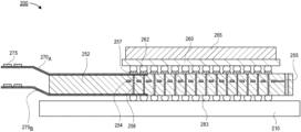
Referring now to FIGS. 2A and 2B, a perspective view illustration and a cross-sectional view illustration of a system 200 that includes an RGA interposer 250 are shown, respectively, in accordance with an embodiment. In an embodiment, the RGA interposer 250 may be substantially similar to the RGA interposer 150 described above with respect to FIGS. 1A and 1B. For example, the RGA interposer 250 may comprise an interposer substrate 252, vias 258, heating elements 254, and pads 257. In an embodiment, a first end of HSIO cables 270 A and 270 B may be integrated into the RGA interposer 250 and be positioned between the pads 257 and the interposer substrate 252 and/or between the vias 258 and the solder balls 283. In an embodiment, the HSIO cables 270 A and 270 B may comprise conductive traces (not shown) that terminate at an array of pads 275.
In an embodiment, the RGA interposer 250 may be electrically and mechanically coupled to a motherboard 210 with solder balls 283. In an embodiment, the RGA interposer 250 may be coupled to the motherboard 210 with standard processes (e.g., a reflow process). In an embodiment, a CPU 265 and CPU package substrate 260 may be coupled to the top surface of the RGA interposer 250 with interconnects 262 (e.g., BGA, LGA, or the like). In an embodiment, the reflow temperature of the interconnects 262 may be lower than the reflow temperature of the solder balls 283. Particularly, the interconnects 262 may have a reflow temperature that is obtainable by activating the heating elements 254 embedded in the interposer substrate 252. Accordingly, the CPU 265 may be attached to the interposer substrate 252 after the assembly of the RGA interposer to 250 to the motherboard 210. For example, a power source may be brought into contact with the heating contacts 255 at any point during assembly (or in the field) in order to initiate reflow of the interconnects 262.
Referring now to FIG. 3A and FIG. 3B, a perspective view illustration and a cross-sectional view illustration of an RGA interposer 350 with dedicated arrays 359 of pads 357 to which HSIO cables 370 may be attached are shown, respectively, in accordance with an embodiment. In an embodiment, the RGA interposer 350 may include a plurality of arrays of pads 357. A first array 356 of pads 357 may be for connecting a CPU (not shown) to the interposer substrate 352. One or more arrays 359 A-C may be for connecting HSIO cables 370. Accordingly, the connection of the HSIO cables 370 to the RGA interposer 350 may be adjacent to the CPU instead of being below the CPU, as shown in the embodiments in FIGS. 2A and 2B. That is, the HSIO cables 370 may be referred to as being adjacent to the CPU in some embodiments. While three arrays 359 A-C are shown in FIG. 3A, it is to be appreciated that any number of arrays 359 may be included in various embodiments. In some embodiments, more arrays 359 than HSIO cables 370 may be included on the RGA interposer 350. The additional arrays 359 allow for additional HSIO cables 370 to be added subsequent to the original assembly (e.g., to allow for expansion at a later time).
In an embodiment, vias 358 may connect the pads 357 in the arrays 359 to signal routing traces 384 that are embedded in the interposer substrate 352. Accordingly, various pads 357 in the first array 356 may be electrically coupled to the pads 357 in the arrays 359 used to attach the HSIO cables 370 to the RGA interposer 350.
In an embodiment, heating elements 354 may also be positioned proximate to the arrays 359. In a particular embodiment, the heating elements 354 may be arranged in zones proximate to each of the arrays 359 A-C. For example, heating contacts 355 may be used to heat one or more zones of heating elements 354. As such, HSIO cables 370 may be added or removed with a localized reflow of interconnects 376 in a single array 359 without causing reflow of interconnects 376 in a neighboring array 359 or the CPU array 356. Therefore, embodiments allow for the RGA interposer 350 to be configured in the late integration phase of system assembly, and the RGA interposer 350 supports enhanced flexibility in system design, reuse, and/or reconfiguration.
Referring now to FIGS. 4A and 4B, a perspective view illustration and a cross-sectional view illustration of a system 400 with an RGA interposer 450 with HSIO cables are shown, respectively, in accordance with an embodiment. In an embodiment, the RGA interposer 450 may be substantially similar to the RGA interposer 350 described above with respect to FIGS. 3A and 3B. For example, the RGA interposer 450 may comprise an interposer substrate 452, vias 458, heating elements 454, heating contacts 455, signal routing traces 484, and pads 457. In an embodiment, a first end of HSIO cables 470 may be attached to one of the arrays 459 A-C on the interposer substrate 452. In an embodiment, the HSIO cables 470 may comprise conductive traces (not shown) that terminate at an array of pads 475.
In an embodiment, the RGA interposer 450 may be electrically and mechanically coupled to a motherboard 410 with solder balls 483. In an embodiment, the RGA interposer 450 may be coupled to the motherboard 410 with standard processes (e.g., a reflow process). In an embodiment, a CPU 465 and CPU package substrate 460 may be coupled to the top surface of the RGA interposer 450 with interconnects 462 (e.g., BGA, LGA, or the like).
In an embodiment, the reflow temperature of the interconnects 462 may be lower than the reflow temperature of the solder balls 483. Particularly, the interconnects 462 may have a reflow temperature that is obtainable by activating the heating elements 454 embedded in the interposer substrate 452. Accordingly, the CPU 465 may be attached to the interposer substrate 452 after the assembly of the RGA interposer to 450 to the motherboard 410. For example, a power source may be brought into contact with the heating contacts 455 at any point during assembly (or in the field) in order to initiate reflow of the interconnects 462. The interconnects 476 that connect the HSIO cable 470 to the pads 457 may also have a lower reflow temperature than the solder balls 483. Accordingly, HSIO cables 470 may also be attached with a reflow process by activating the heaters 454 proximate to the desired array 459 of pads 457. As such, HSIO cables 470 may be attached to the interposer substrate 452 after the assembly of the RGA interposer to 450 to the motherboard 410. For example, a power source may be brought into contact with the heating contacts 455 at any point during assembly (or in the field) in order to initiate reflow of the interconnects 476.
Referring now to FIG. 5 , a perspective view illustration of a system 500 with an HSIO cable 570 that provide a communication link between a first CPU 565 A and a second CPU 565 B is shown, in accordance with an embodiment. In an embodiment, the system 500 may comprise a first RGA interposer 550 A and a second RGA interposer 550 B. As shown, the RGA interposers 550 A and 550 B may be substantially similar to the RGA interposer 450 described above with respect to FIG. 4A. For example, the RGA interposers 550 may comprise a plurality of arrays (e.g., arrays 559 AA-BC) to which HSIO cables 570 may be connected. The arrays 559 AA-BC may each comprise their own zone of heaters (embedded in the interposer substrate 552 A or 552 B) that are connected to heater contacts 555. Additionally, a CPU 565 and CPU package 560 may be attached to each RGA interposer 550. For example, CPU 565 A and CPU package 560 A may be attached to RGA interposer 550 A and CPU 565 B and CPU package 560 B may be attached to RGA interposer 550 B. In an embodiment, the first RGA interposer 550 A and the second RGA interposer 550 B may be attached to a motherboard 510. In other embodiments, the first RGA interposer 550 A and the second RGA interposer 550 B may be attached to different motherboards 510.
In an embodiment, a first end of the HSIO cable 570 is attached to an array 559 AA on the first RGA interposer 550 A and a second end of the HSIO cable 570 is attached to an array 559 BA on the second RGA interposer 550 B. Accordingly, the CPUs 565 A and 565 B may be able to communicate with each other over the HSIO cable 570. While a single HSIO cable 570 is shown, it is to be appreciated that any number of HSIO cables 570 may be used to provide a communication link between the RGA interposers 550 A and 550 B. Furthermore, each RGA interposer 550 may have communication links provided by an HSIO cable 570 to any number of RGA interposers 550 (e.g., one or more different RGA interposers 550). Additionally, while the HSIO cable 570 is shown as connecting two RGA interposers 550 A and 550 B, it is to be appreciated that similar HSIO cables 570 may be used to attach an RGA interposer 550 to any other device. That is, an RGA interposer 550 may be coupled to a device that does not include an RGA interposer 550 by an HSIO cable 570.
While system 500 is shown using RGA interposers 550 that are similar to those shown in FIGS. 3A and 3B, it is to be appreciated that any RGA interposers may be connected with HSIO cables 570. For example, the HSIO cables 570 may be integrated into the interposer substrate, similar to the embodiments shown in FIGS. 1A and 1B.
Referring now to FIG. 6 , a cross-sectional illustration of a system 600 with an RGA interposer 650 is shown, in accordance with an embodiment. In an embodiment, the system 600 may be similar to the system 400 shown in FIG. 4B, with the exception that the HSIO cable 670 is coupled to the RGA interposer 650 through an electrical-to-optical converter die 690. The electrical-to-optical converter die 690 may convert electrical signals from the CPU 665 to an optical signal that may then be transmitted along the HSIO cable 670. For example, the HSIO cable 670 may be an optical cable (e.g., a fiber optic cable or bundle to fiber optic cables). The conversion to an optical signal may allow for even higher communication speeds.
Similar to system 400, system 600 may also include an RGA interposer 650 that is substantially similar to the RGA interposer 450 that is coupled to a motherboard 610 with solder balls 683. The RGA interposer 650 may comprise an interposer substrate 652. Vias 658 and signal routing traces 684 may be embedded in the interposer substrate 652 to allow communication between pads 657 to which the electrical-to-optical converter die 690 is attached (with interconnects 676) and pads 657 to which the CPU package 660 is attached (with interconnects 662). In an embodiment, the RGA interposer 650 may also include heating elements 654 that are coupled to heating contacts 655.
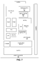
FIG. 7 illustrates a computing device 700 in accordance with one implementation of the invention. The computing device 700 houses a board 702. The board 702 may include a number of components, including but not limited to a processor 704 and at least one communication chip 706. The processor 704 is physically and electrically coupled to the board 702. In some implementations the at least one communication chip 706 is also physically and electrically coupled to the board 702. In further implementations, the communication chip 706 is part of the processor 704.
These other components include, but are not limited to, volatile memory (e.g., DRAM), non-volatile memory (e.g., ROM), flash memory, a graphics processor, a digital signal processor, a crypto processor, a chipset, an antenna, a display, a touchscreen display, a touchscreen controller, a battery, an audio codec, a video codec, a power amplifier, a global positioning system (GPS) device, a compass, an accelerometer, a gyroscope, a speaker, a camera, and a mass storage device (such as hard disk drive, compact disk (CD), digital versatile disk (DVD), and so forth).
The communication chip 706 enables wireless communications for the transfer of data to and from the computing device 700. The term “wireless” and its derivatives may be used to describe circuits, devices, systems, methods, techniques, communications channels, etc., that may communicate data through the use of modulated electromagnetic radiation through a non-solid medium. The term does not imply that the associated devices do not contain any wires, although in some embodiments they might not. The communication chip 706 may implement any of a number of wireless standards or protocols, including but not limited to Wi-Fi (IEEE 802.11 family), WiMAX (IEEE 802.16 family), IEEE 802.20, long term evolution (LTE), Ev-DO, HSPA+, HSDPA+, HSUPA+, EDGE, GSM, GPRS, CDMA, TDMA, DECT, Bluetooth, derivatives thereof, as well as any other wireless protocols that are designated as 3G, 4G, 5G, and beyond. The computing device 700 may include a plurality of communication chips 706. For instance, a first communication chip 706 may be dedicated to shorter range wireless communications such as Wi-Fi and Bluetooth and a second communication chip 706 may be dedicated to longer range wireless communications such as GPS, EDGE, GPRS, CDMA, WiMAX, LTE, Ev-DO, and others.
The processor 704 of the computing device 700 includes an integrated circuit die packaged within the processor 704. In some implementations of the invention, the integrated circuit die of the processor may be packaged in an electronic system that comprises an RGA interposer with an HSIO cable, in accordance with embodiments described herein. The term “processor” may refer to any device or portion of a device that processes electronic data from registers and/or memory to transform that electronic data into other electronic data that may be stored in registers and/or memory.
The communication chip 706 also includes an integrated circuit die packaged within the communication chip 706. In accordance with another implementation of the invention, the integrated circuit die of the communication chip may be packaged in an electronic system that comprises an RGA interposer with an HSIO cable, in accordance with embodiments described herein.
The above description of illustrated implementations of the invention, including what is described in the Abstract, is not intended to be exhaustive or to limit the invention to the precise forms disclosed. While specific implementations of, and examples for, the invention are described herein for illustrative purposes, various equivalent modifications are possible within the scope of the invention, as those skilled in the relevant art will recognize.
These modifications may be made to the invention in light of the above detailed description. The terms used in the following claims should not be construed to limit the invention to the specific implementations disclosed in the specification and the claims. Rather, the scope of the invention is to be determined entirely by the following claims, which are to be construed in accordance with established doctrines of claim interpretation.
Example 1: an interposer, comprising: an interposer substrate; an array of pads on a first surface of the interposer substrate; a plurality of vias through the interposer substrate, wherein each via is electrically coupled to one of the pads in the array of pads; a plurality of heating elements embedded in the interposer substrate; and a first cable over the first surface interposer substrate, the first cable comprising: an array of conductive lines along the first cable, wherein conductive lines proximate to a first end of the cable are electrically coupled to pads in the array of pads.
Example 2: the interposer of Example 1, wherein the first cable is between the pads and the first surface of the interposer.
Example 3: the interposer of Examples 1-3, wherein the first cable is a flexible cable.
Example 4: the interposer of Examples 1-4, wherein the flexible cable comprises a polyamide sheet.
Example 5: the interposer of Examples 1-5, further comprising: a second cable over a second surface of the interposer substrate, wherein the second cable comprises an array of conductive lines along the second cable, wherein the conductive lines proximate to a first end of the second cable are electrically coupled to vias through the interposer substrate.
Example 6: the interposer of Examples 1-5, wherein the first cable and the second cable are offset from each other.
Example 7: the interposer of Examples 1-6, wherein the first cable and the second cable extend away from the same edge of the array of pads.
Example 8: an interposer, comprising: an interposer substrate; a first array of pads on a first surface of the interposer substrate; a plurality of vias through the interposer substrate, wherein each via is electrically coupled to one of the pads in the first array of pads; a plurality of heating elements embedded in the interposer substrate; a second array of pads on the first surface of the interposer substrate, wherein pads in the second array of pads are electrically coupled to pads in the first array of pads through conductive traces embedded in the interposer substrate; and a first cable electrically coupled to the second array of pads.
Example 9: the interposer of Example 8, wherein the first cable is a flexible cable.
Example 10: the interposer of Example 8 or Example 9, wherein the flexible cable comprises a polyamide sheet.
Example 11: the interposer of Examples 8-10, further comprising: a third array of pads on the first surface of the interposer substrate, wherein pads in the third array of pads are electrically coupled to pads in the first array of pads through conductive traces embedded in the interposer substrate.
Example 12: the interposer of Examples 8-11, further comprising: a second cable electrically coupled to the pads in the third array of pads.
Example 13: the interposer of Examples 8-12, wherein the first cable is electrically coupled to the second array of pads by an electrical-to-optical converter die.
Example 14: the interposer of Examples 8-13, wherein the first cable is an optical cable.
Example 15: the interposer of Examples 8-14, wherein the plurality of heating elements comprises a first zone of heating elements proximate to the pads in the first array of pads, and a second zone of heating elements proximate to the pads in the second array of pads, and wherein the first zone and the second zone are independently operated.
Example 16: an electronic package, comprising: a motherboard; a first interposer over the motherboard; a first die electrically coupled to the first interposer; a second interposer over the motherboard; a second die electrically coupled to the second interposer; and a cable attached between the first interposer and the second interposer, wherein the cable provides a communication pathway between the first die and the second die that does not pass through the motherboard.
Example 17: the electronic package of Example 16, wherein the cable is a flexible cable.
Example 18: the electronic package of Example 16 or Example 17, wherein the cable comprises a polyamide sheet.
Example 19: the electronic package of Examples 16-18, wherein the first interposer and the second interposer both comprise embedded heaters.
Example 20: the electronic package of Examples 16-19, wherein the embedded heaters comprise a plurality of zones.
Example 21: the electronic package of Examples 16-20, wherein a first end of the cable is attached to the first interposer between the first die and the first interposer, and wherein a second end of the cable is attached to the second interposer between the second die and the second interposer.
Example 22: the electronic package of Examples 16-21, wherein a first end of the cable is attached to an array of pads on the first interposer that is adjacent to the first die, and wherein a second end of the cable is attached to an array of pads on the second interposer that is adjacent to the second die.
Example 23: the electronic package of Examples 16-22, wherein the first die and the second die are processor dies.
Example 24: the electronic package of Examples 16-23, wherein the cable provides signaling speeds of 50 GHz or greater.
Example 25: the electronic package of Examples 16-24, wherein the cable is an optical cable.

Claims (23)

What is claimed is:
1. An interposer, comprising:
an interposer substrate;
an array of pads on a first surface of the interposer substrate;
a plurality of vias through the interposer substrate, wherein each via is electrically coupled to one of the pads in the array of pads;
a plurality of heating elements embedded in the interposer substrate; and
a first cable over the first surface interposer substrate, the first cable comprising:
an array of conductive lines along the first cable, wherein conductive lines proximate to a first end of the cable are electrically coupled to pads in the array of pads, and wherein the first cable vertically overlaps with at least a portion of the plurality of heating elements.
2. The interposer of claim 1, wherein the first cable is between the pads and the first surface of the interposer.
3. The interposer of claim 1, wherein the first cable is a flexible cable.
4. The interposer of claim 1, further comprising:
a second cable over a second surface of the interposer substrate, wherein the second cable comprises an array of conductive lines along the second cable, wherein the conductive lines proximate to a first end of the second cable are electrically coupled to vias through the interposer substrate.
5. The interposer of claim 3, wherein the flexible cable comprises a polyamide sheet.
6. The interposer of claim 4, wherein the first cable and the second cable are offset from each other.
7. The interposer of claim 4, wherein the first cable and the second cable extend away from the same edge of the array of pads.
8. An interposer, comprising:
an interposer substrate;
a first array of pads on a first surface of the interposer substrate;
a plurality of vias through the interposer substrate, wherein each via is electrically coupled to one of the pads in the first array of pads;
a plurality of heating elements embedded in the interposer substrate;
a second array of pads on the first surface of the interposer substrate, wherein pads in the second array of pads are electrically coupled to pads in the first array of pads through conductive traces embedded in the interposer substrate; and
a first cable electrically coupled to the second array of pads, wherein the first cable vertically overlaps with at least a portion of the plurality of heating elements.
9. The interposer of claim 8, wherein the first cable is a flexible cable.
10. The interposer of claim 8, further comprising:
a third array of pads on the first surface of the interposer substrate, wherein pads in the third array of pads are electrically coupled to pads in the first array of pads through conductive traces embedded in the interposer substrate.
11. The interposer of claim 8, wherein the first cable is electrically coupled to the second array of pads by an electrical-to-optical converter die.
12. The interposer of claim 8, wherein the plurality of heating elements comprises a first zone of heating elements proximate to the pads in the first array of pads, and a second zone of heating elements proximate to the pads in the second array of pads, and wherein the first zone and the second zone are independently operated.
13. The interposer of claim 9, wherein the flexible cable comprises a polyamide sheet.
14. The interposer of claim 11, wherein the first cable is an optical cable.
15. An electronic package, comprising:
a motherboard;
a first interposer over the motherboard;
a first die electrically coupled to the first interposer;
a second interposer over the motherboard, wherein the first interposer and the second interposer both comprise embedded heaters;
a second die electrically coupled to the second interposer; and
a cable attached between the first interposer and the second interposer, wherein the cable provides a communication pathway between the first die and the second die that does not pass through the motherboard, and wherein the cable vertically overlaps with at least a portion of the embedded heaters in the first interposer or the second interposer.
16. The electronic package of claim 15, wherein the cable is a flexible cable.
17. The electronic package of claim 15, wherein the cable comprises a polyamide sheet.
18. The electronic package of claim 15, wherein the embedded heaters comprise a plurality of zones.
19. The electronic package of claim 15, wherein a first end of the cable is attached to the first interposer between the first die and the first interposer, and wherein a second end of the cable is attached to the second interposer between the second die and the second interposer.
20. The electronic package of claim 15, wherein a first end of the cable is attached to an array of pads on the first interposer that is adjacent to the first die, and wherein a second end of the cable is attached to an array of pads on the second interposer that is adjacent to the second die.
21. The electronic package of claim 15, wherein the first die and the second die are processor dies.
22. The electronic package of claim 15, wherein the cable provides signaling speeds of 50 GHz or greater.
23. The electronic package of claim 15, wherein the cable is an optical cable.
US16/247,312 2019-01-14 2019-01-14 Interposer and electronic package Active 2041-08-04 US11621237B2 (en)

Priority Applications (1)

Application Number Priority Date Filing Date Title
US16/247,312 US11621237B2 (en) 2019-01-14 2019-01-14 Interposer and electronic package

Applications Claiming Priority (1)

Application Number Priority Date Filing Date Title
US16/247,312 US11621237B2 (en) 2019-01-14 2019-01-14 Interposer and electronic package

Publications (2)

Publication Number Publication Date
US20200227362A1 US20200227362A1 (en) 2020-07-16
US11621237B2 true US11621237B2 (en) 2023-04-04

Family

ID=71516136

Family Applications (1)

Application Number Title Priority Date Filing Date
US16/247,312 Active 2041-08-04 US11621237B2 (en) 2019-01-14 2019-01-14 Interposer and electronic package

Country Status (1)

Country Link
US (1) US11621237B2 (en)

Families Citing this family (3)

* Cited by examiner, † Cited by third party
Publication number Priority date Publication date Assignee Title
TWI698964B (en) * 2019-03-15 2020-07-11 台灣愛司帝科技股份有限公司 Chip fastening structure and chip fastening apparatus
TWI698949B (en) * 2019-08-07 2020-07-11 台灣愛司帝科技股份有限公司 Film structure, chip carrier assembly and chip carrier device
US11693814B2 (en) * 2020-12-18 2023-07-04 Quanta Computer Inc. Systems and methods for expanding memory access

Citations (18)

* Cited by examiner, † Cited by third party
Publication number Priority date Publication date Assignee Title
US5574630A (en) * 1995-05-11 1996-11-12 International Business Machines Corporation Laminated electronic package including a power/ground assembly
US5784262A (en) * 1995-11-06 1998-07-21 Symbios, Inc. Arrangement of pads and through-holes for semiconductor packages
US6586684B2 (en) * 2001-06-29 2003-07-01 Intel Corporation Circuit housing clamp and method of manufacture therefor
US6797891B1 (en) * 2002-03-18 2004-09-28 Applied Micro Circuits Corporation Flexible interconnect cable with high frequency electrical transmission line
US6853061B2 (en) * 2002-10-18 2005-02-08 Intel Corporation Dual power supply method and apparatus
US6940729B2 (en) * 2001-10-26 2005-09-06 Staktek Group L.P. Integrated circuit stacking system and method
US6985659B2 (en) * 2003-06-30 2006-01-10 Opnext Japan, Inc. Optical transmission module
US20060065431A1 (en) * 2004-09-29 2006-03-30 Trucco Horacio A Self-reflowing printed circuit board and application methods
US7345359B2 (en) * 2004-03-05 2008-03-18 Intel Corporation Integrated circuit package with chip-side signal connections
US7474540B1 (en) * 2008-01-10 2009-01-06 International Business Machines Corporation Silicon carrier including an integrated heater for die rework and wafer probe
US7750446B2 (en) * 2002-04-29 2010-07-06 Interconnect Portfolio Llc IC package structures having separate circuit interconnection structures and assemblies constructed thereof
US20110121922A1 (en) * 2002-03-18 2011-05-26 Qualcomm Incorporated Flexible interconnect cable for an electronic assembly
US8059424B2 (en) * 2007-01-31 2011-11-15 Hispano Suiza Electronic board incorporating a heating resistor
US20130045611A1 (en) * 2011-08-18 2013-02-21 Tyco Electronics Corporation Electronic module packages and communication assemblies
US20170179067A1 (en) * 2015-12-18 2017-06-22 Intel Corporation Semiconductor package alignment frame for local reflow
US20170186661A1 (en) * 2015-12-23 2017-06-29 Intel Corporation Rework grid array interposer with direct power
US20180350767A1 (en) * 2015-12-18 2018-12-06 Intel Corporation Ball grid array solder attachment
US20180352649A1 (en) * 2015-12-21 2018-12-06 Intel Corporation Connector interface for processor packaging

Patent Citations (18)

* Cited by examiner, † Cited by third party
Publication number Priority date Publication date Assignee Title
US5574630A (en) * 1995-05-11 1996-11-12 International Business Machines Corporation Laminated electronic package including a power/ground assembly
US5784262A (en) * 1995-11-06 1998-07-21 Symbios, Inc. Arrangement of pads and through-holes for semiconductor packages
US6586684B2 (en) * 2001-06-29 2003-07-01 Intel Corporation Circuit housing clamp and method of manufacture therefor
US6940729B2 (en) * 2001-10-26 2005-09-06 Staktek Group L.P. Integrated circuit stacking system and method
US6797891B1 (en) * 2002-03-18 2004-09-28 Applied Micro Circuits Corporation Flexible interconnect cable with high frequency electrical transmission line
US20110121922A1 (en) * 2002-03-18 2011-05-26 Qualcomm Incorporated Flexible interconnect cable for an electronic assembly
US7750446B2 (en) * 2002-04-29 2010-07-06 Interconnect Portfolio Llc IC package structures having separate circuit interconnection structures and assemblies constructed thereof
US6853061B2 (en) * 2002-10-18 2005-02-08 Intel Corporation Dual power supply method and apparatus
US6985659B2 (en) * 2003-06-30 2006-01-10 Opnext Japan, Inc. Optical transmission module
US7345359B2 (en) * 2004-03-05 2008-03-18 Intel Corporation Integrated circuit package with chip-side signal connections
US20060065431A1 (en) * 2004-09-29 2006-03-30 Trucco Horacio A Self-reflowing printed circuit board and application methods
US8059424B2 (en) * 2007-01-31 2011-11-15 Hispano Suiza Electronic board incorporating a heating resistor
US7474540B1 (en) * 2008-01-10 2009-01-06 International Business Machines Corporation Silicon carrier including an integrated heater for die rework and wafer probe
US20130045611A1 (en) * 2011-08-18 2013-02-21 Tyco Electronics Corporation Electronic module packages and communication assemblies
US20170179067A1 (en) * 2015-12-18 2017-06-22 Intel Corporation Semiconductor package alignment frame for local reflow
US20180350767A1 (en) * 2015-12-18 2018-12-06 Intel Corporation Ball grid array solder attachment
US20180352649A1 (en) * 2015-12-21 2018-12-06 Intel Corporation Connector interface for processor packaging
US20170186661A1 (en) * 2015-12-23 2017-06-29 Intel Corporation Rework grid array interposer with direct power

Also Published As

Publication number Publication date
US20200227362A1 (en) 2020-07-16

Similar Documents

Publication Publication Date Title
US11742275B2 (en) Ground via clustering for crosstalk mitigation
CN107924914B (en) Platform with thermally stable wireless interconnect
US9589866B2 (en) Bridge interconnect with air gap in package assembly
TWI466268B (en) Proximity communication package for processor, cache and memory
US11621237B2 (en) Interposer and electronic package
US8290319B2 (en) Optical communication in a ramp-stack chip package
US8283766B2 (en) Ramp-stack chip package with static bends
TWI699106B (en) Patch on interposer package with wireless communication interface
US20240088047A1 (en) Scalable high speed high bandwidth io signaling package architecture and method of making
CN108370083B (en) Antenna for platform level wireless interconnect
US10452571B2 (en) Microelectronic package communication using radio interfaces connected through waveguides
CN106797098B (en) Socket contact technology and construction
KR20200113186A (en) Antenna module and communication device
US20160093340A1 (en) Compact microelectronic assembly having reduced spacing between controller and memory packages
JP2017503360A (en) Opossum die-type package-on-package equipment
US10276483B2 (en) Coaxial vias
US20130313727A1 (en) Multi-stacked bbul package
US10992021B2 (en) Cross talk and interference reduction for high frequency wireless interconnects
EP4020028A1 (en) Stackable photonics die with direct optical interconnect
US11569161B2 (en) Integrated memory coplanar transmission line package having ground path that brackets data path to extend memory speeds
US20190307009A1 (en) Selective ground flood around reduced land pad on package base layer to enable high speed land grid array (lga) socket
US20240006286A1 (en) Layer selection for routing high-speed signals in substrates
JP2021153174A (en) Package land pad in closed-loop trace for high-speed data signaling
CN117525046A (en) Semiconductor package and method based on die interconnection

Legal Events

Date Code Title Description
FEPP Fee payment procedure

Free format text: ENTITY STATUS SET TO UNDISCOUNTED (ORIGINAL EVENT CODE: BIG.); ENTITY STATUS OF PATENT OWNER: LARGE ENTITY

AS Assignment

Owner name: INTEL CORPORATION, CALIFORNIA

Free format text: ASSIGNMENT OF ASSIGNORS INTEREST;ASSIGNORS:THIBADO, JONATHAN W.;SMALLEY, JEFFORY L.;GULICK, JOHN C.;AND OTHERS;SIGNING DATES FROM 20190108 TO 20190114;REEL/FRAME:051022/0297

STPP Information on status: patent application and granting procedure in general

Free format text: NON FINAL ACTION MAILED

STPP Information on status: patent application and granting procedure in general

Free format text: RESPONSE TO NON-FINAL OFFICE ACTION ENTERED AND FORWARDED TO EXAMINER

STPP Information on status: patent application and granting procedure in general

Free format text: NON FINAL ACTION MAILED

STPP Information on status: patent application and granting procedure in general

Free format text: RESPONSE TO NON-FINAL OFFICE ACTION ENTERED AND FORWARDED TO EXAMINER

STPP Information on status: patent application and granting procedure in general

Free format text: NOTICE OF ALLOWANCE MAILED -- APPLICATION RECEIVED IN OFFICE OF PUBLICATIONS

STCF Information on status: patent grant

Free format text: PATENTED CASE