US11609130B2 - Cantilever force sensor - Google Patents

Cantilever force sensor Download PDF

Info

Publication number
US11609130B2
US11609130B2 US17/152,668 US202117152668A US11609130B2 US 11609130 B2 US11609130 B2 US 11609130B2 US 202117152668 A US202117152668 A US 202117152668A US 11609130 B2 US11609130 B2 US 11609130B2
Authority
US
United States
Prior art keywords
stack
force sensor
spacer
substrate
electrode
Prior art date
Legal status (The legal status is an assumption and is not a legal conclusion. Google has not performed a legal analysis and makes no representation as to the accuracy of the status listed.)
Active, expires
Application number
US17/152,668
Other versions
US20220228931A1 (en
Inventor
Chih-Sheng Hou
Chia-Hung Chou
Current Assignee (The listed assignees may be inaccurate. Google has not performed a legal analysis and makes no representation or warranty as to the accuracy of the list.)
Uneo Inc
Original Assignee
Uneo Inc
Priority date (The priority date is an assumption and is not a legal conclusion. Google has not performed a legal analysis and makes no representation as to the accuracy of the date listed.)
Filing date
Publication date
Application filed by Uneo Inc filed Critical Uneo Inc
Priority to US17/152,668 priority Critical patent/US11609130B2/en
Assigned to UNEO INC. reassignment UNEO INC. ASSIGNMENT OF ASSIGNORS INTEREST (SEE DOCUMENT FOR DETAILS). Assignors: HOU, CHIH-SHENG, CHOU, CHIA-HUNG
Priority to CN202110432914.5A priority patent/CN114812880A/en
Publication of US20220228931A1 publication Critical patent/US20220228931A1/en
Priority to US18/162,719 priority patent/US20230168138A1/en
Application granted granted Critical
Publication of US11609130B2 publication Critical patent/US11609130B2/en
Active legal-status Critical Current
Adjusted expiration legal-status Critical

Links

Images

Classifications

    • GPHYSICS
    • G01MEASURING; TESTING
    • G01LMEASURING FORCE, STRESS, TORQUE, WORK, MECHANICAL POWER, MECHANICAL EFFICIENCY, OR FLUID PRESSURE
    • G01L1/00Measuring force or stress, in general
    • G01L1/16Measuring force or stress, in general using properties of piezoelectric devices
    • GPHYSICS
    • G01MEASURING; TESTING
    • G01LMEASURING FORCE, STRESS, TORQUE, WORK, MECHANICAL POWER, MECHANICAL EFFICIENCY, OR FLUID PRESSURE
    • G01L1/00Measuring force or stress, in general
    • G01L1/20Measuring force or stress, in general by measuring variations in ohmic resistance of solid materials or of electrically-conductive fluids; by making use of electrokinetic cells, i.e. liquid-containing cells wherein an electrical potential is produced or varied upon the application of stress
    • GPHYSICS
    • G01MEASURING; TESTING
    • G01LMEASURING FORCE, STRESS, TORQUE, WORK, MECHANICAL POWER, MECHANICAL EFFICIENCY, OR FLUID PRESSURE
    • G01L1/00Measuring force or stress, in general
    • G01L1/18Measuring force or stress, in general using properties of piezo-resistive materials, i.e. materials of which the ohmic resistance varies according to changes in magnitude or direction of force applied to the material

Abstract

A cantilever force sensor with relatively lower On-Force is disclosed, which comprises a top stack, a bottom stack, and a spacer. The first spacer is configured between the top stack and the bottom stack and configured in a first side of the force sensor. A second side, opposite to the first side, of the top stack, is cantilevered from the bottom stack. When the force sensor is depressed from the top side, the second side of the top stack moves down using the first spacer as a fulcrum. Since the cantilevered side can be easily depressed down so that the On-Force for the force sensor is reduced and hence a force sensor with a relatively higher sensitivity is created.

Description

BACKGROUND Technical Field
The present invention relates to a force sensor, especially relates to a cantilever force sensor which can be turned on with a relatively reduced on-force so that a force sensor with higher sensitivity is created.
Description of Related Art
FIG. 1A˜1D shows a prior art.
Referring to FIG. 1A as disclosed in U.S. Pat. No. 8,371,174, a conventional force sensor comprises a top substrate 10 and a bottom substrate 109, a top electrode 11 is configured on a bottom side of the top substrate 10. A bottom electrode 119 is configured on the top side of the bottom substrate 109. A top piezoresistive layer 12 is configured on the bottom side of the top electrode 11. A bottom piezoresistive layer 129 is configured on the top side of the bottom electrode 119. A space 16 is formed between the two piezoresistive layers 12, 129. As shown in FIG. 1A, a ring spacer 15 is configured between the substrates 10 and 109. The top electrode 11 and bottom electrode 119 are electrically connected to a circuit system 13.
FIG. 1B shows an EE′ section view of the prior art FIG. 1A.
FIG. 1B shows that a ring spacer 15 is configured around the force sensor. The ring spacer 15 resists more against a force applied from the top side of the force sensor.
FIG. 1C shows when a force P is applied to the force sensor of FIG. 1A, the top piezoresistive layer 12 deforms downwardly in the middle portion and contacts the bottom piezoresistive layer 129, at this moment, the piezoresistive layers 12 and 129 have a total thickness of L1. Hence, an output resistance R1 of the force sensor can be determined by the equation R1=p*L1/A.
FIG. 1D shows an electricity property for the prior art.
FIG. 1D shows a curve for Conductance/Capacitance vs Force for FIG. 1C. Referring to FIG. 1D a status when the force sensor is depressed from the top side, at the moment of FIG. 1C, an On-Force starts at point P1 which is apparently greater than the zero force point. This is because the ring spacer 15 resists the force applied from the top of the force sensor.
A disadvantage for the prior art is that an On-Force is relatively greater because the ring spacer 15 gives more resistance to the force applied from the top side. It is hopeful for a person skilled in the art to reduce the On-Force so that a force sensor with a higher sensitivity can be obtained.
BRIEF DESCRIPTION OF THE DRAWINGS
FIG. 1A˜1D shows a prior art.
FIG. 2A˜2D shows a first embodiment according to the present invention.
FIG. 3 shows the first embodiment configured in an electronic pen according to the present invention.
FIG. 4A˜4B shows a second embodiment according to the present invention.
FIG. 5 shows a third embodiment according to the present invention.
FIG. 6 shows a fourth embodiment according to the present invention.
FIG. 7 shows a fifth embodiment according to the present invention.
FIG. 8 shows a sixth embodiment according to the present invention.
FIG. 9 shows a seventh embodiment according to the present invention.
FIG. 10A˜10B shows an eighth embodiment according to the present invention.
FIG. 11A˜11B shows a ninth embodiment according to the present invention.
FIG. 12A˜12B shows a tenth embodiment according to the present invention.
FIG. 13A˜13B shows an eleventh embodiment according to the present invention.
FIG. 14A˜14B shows a twelfth embodiment according to the present invention.
FIG. 15 shows a thirteenth embodiment according to the present invention.
FIG. 16 shows a fourteen embodiment according to the present invention.
FIG. 17 shows a fifteen embodiment according to the present invention.
DETAILED DESCRIPTION OF THE INVENTION
FIG. 2A˜2D shows a first embodiment according to the present invention.
FIG. 2A shows a cantilever force sensor FS with a bottom switch SW configured on the bottom side of the force sensor FS. The force sensor FS comprises a top stack TS, a first spacer S1, and a bottom stack BS in sequence. A first gap G1 is configured between the top stack TS and the bottom stack BS. The first spacer S1 is configured in the right side of the force sensor FS. The left side of the top stack TS is cantilevered from the bottom stack BS.
When the force sensor FS is depressed from the top side, the left side of the top stack TS moves down using the first spacer 51 as a fulcrum to turn on the force sensor FS. The first spacer S1 has a top end connected to the top piezo layer 22 of the top stack TS and has a bottom end connected to the bottom piezo electrode 24 of the bottom stack BS.
The top stack TS is comprised of a top substrate 20, a top electrode 21, and a top piezo layer 22 in sequence. The bottom stack BS is comprised of a bottom piezo layer 23, a bottom electrode 24, and a bottom substrate 25 in sequence.
A bottom switch SW is configured on the bottom side of the force sensor FS. A first conductive contact C1 is configured on the bottom side of the bottom stack BS of the force sensor FS. A second conductive contact C2, aligned with the first conductive contact C1, is configured on a top side of a printed circuit board 26 of the bottom switch SW. A second spacer S2 is configured between the bottom substrate 25 and the printed circuit board 26, and the second spacer S2 is configured in the right side of the bottom switch SW. The bottom stack BS, the first conductive contact C1, the second conductive contact C2, and the printed circuit board 26 are configured in sequence to form the bottom switch SW. The delayed turn-on switch is designed for shielding the initial noise signal from the force sensor at an initial stage when it is depressed.
The first conductive contact C1 slightly touches the second conductive contact C2, however without turns on the bottom switch SW. When the force sensor FS is depressed from the top side, the left side of the force sensor FS moves down so that the first conductive contact C1 touches the second conductive contact C2 firmly to turn on the bottom switch SW.
FIG. 2B shows an AA′ section view of FIG. 2A according to the present invention. The first spacer S1 is configured in the right side of the force sensor FS, and configured between the top stack TS and the bottom stack BS of the force sensor FS.
FIG. 2C shows the force sensor being depressed according to the present invention. The top stack TS moves down on its left side using the first spacer S1 as a fulcrum when the force sensor FS is depressed from the top side. After the top stack TS touches the bottom stack BS, a force signal is sent to a control center (not shown) for signal processing.
FIG. 2D shows an electrical property for the first embodiment according to the present invention. FIG. 2D shows a curve for Conductance/Capacitance vs Force for the first embodiment. Referring to FIG. 2C a status when the force sensor FS is depressed from the top side, an On-Force starts at point P2 which is extremely near to zero force point. This is because that a single side spacer S1 is configured in the right side of the force sensor FS. The cantilevered top stack TS of the force sensor FS reduces On-Force.
FIG. 3 shows the first embodiment configured in an electronic pen according to the present invention.
FIG. 3 shows that the force sensor FS with a bottom switch SW can be configured on the bottom side of the pen tip 61 of an electronic pen to sense forces coming from the pen tip 61 when the electronic pen is writing with its pen tip 61.
FIG. 4A˜4B shows a second embodiment according to the present invention.
FIG. 4A shows a modified embodiment to the first embodiment of FIG. 2A with a different position for the first spacer S1. FIG. 4A shows that the first spacer S1 is configured between the top stack TS and the bottom stack BS and configured in the right side of the force sensor FS. The spacer S1 has a top end connected to the top substrate 20 and has a bottom end connected to the bottom substrate 25.
FIG. 4B shows a BB′ section view of FIG. 4A according to the present invention. The first spacer S1 is configured in the right side of the force sensor FS, and configured between the top stack TS and the bottom stack BS.
FIG. 5 shows a third embodiment according to the present invention.
FIG. 5 shows a further modified embodiment to the first embodiment with a different position for the first spacer S1. The first spacer S1 is configured between the top stack TS and the bottom stack BS and configured in the right side of the force sensor FS. The spacer S1 has a top end connected to the top piezo layer 22 and has a bottom end connects to the bottom substrate 25.
FIG. 6 shows a fourth embodiment according to the present invention.
FIG. 6 shows a further modified embodiment to the first embodiment with a different position for the first spacer S1. The first spacer S1 is configured between the top stack TS and the bottom stack BS and configured in the right side of the force sensor FS. The spacer S1 has a top end connected to the top substrate 20 and has a bottom end connected to the bottom piezo layer 23.
FIG. 7 shows a fifth embodiment according to the present invention.
FIG. 7 shows a further modified embodiment of the force sensor FS with a modified bottom switch configured in an electronic pen. The force sensor FS with a bottom switch SW can be configured in the bottom side of the pen tip 61 of an electronic pen to sense forces coming from the pen tip 61 when the electronic pen is writing with its pen tip 61. The first conductive contact C1 under the force sensor FS is configured slightly apart from the second conductive contact C2. When the force sensor FS is depressed from the top side, the left side of the bottom stack BS moves down so that the first conductive contact C1 touches the second conductive contact C2 firmly to turn on the bottom switch SW. The delayed turn-on switch is designed for shielding the initial noise signal from the force sensor FS at an initial stage when the force sensor FS is depressed.
FIG. 8 shows a sixth embodiment according to the present invention.
FIG. 8 shows a further modified embodiment to the first embodiment. A single piezo layer, a top piezo layer 22, is configured in the force sensor FS. The top stack TS is comprised of a top substrate 20, a top electrode 21, and a top piezo layer 22 in sequence. The bottom stack BS is comprised of a bottom electrode 24 and a bottom substrate 25 in sequence and without having any piezo layer configured in the bottom stack BS.
The first spacer S1 is configured between the top stack TS and the bottom stack BS and configured in the right side of the force sensor FS. A first gap G1 is configured between the top stack TS and the bottom stack BS. The first spacer S1 has a top end connected to the top piezo layer 22 of the top stack TS and has a bottom end connected to the bottom electrode 24 of the bottom stack BS.
FIG. 9 shows a seventh embodiment according to the present invention.
FIG. 9 shows a modified embodiment to the first embodiment. A single piezo layer, a bottom piezo layer 23, is configured in the force sensor FS. The top stack TS is comprised of a top substrate 20, and a top electrode 21 in sequence. The bottom stack BS is comprised of a bottom piezo layer 23, a bottom electrode 24, and a bottom substrate 25 in sequence.
The first spacer S1 is configured between the top stack TS and the bottom stack BS and configured in the right side of the force sensor FS. A first gap G1 is configured between the top stack TS and the bottom stack BS. The first spacer S1 has a top end connected to the top electrode 21 of the top stack TS and has a bottom end connected to the bottom piezo layer 23 of the bottom stack BS.
FIG. 10A˜10B shows an eighth embodiment according to the present invention.
FIG. 10A shows a modified embodiment to the first embodiment. FIG. 10A shows a front view of the modified embodiment where a single piezo layer, a bottom piezo layer 23, is configured in the bottom stack BS of the force sensor FS. A pair of coplanar electrodes 241, 242 is configured on the bottom side of the bottom piezo layer 23, and the bottom substrate 25 is configured on the bottom side of the coplanar electrodes 241, 242.
The top stack TS is comprised of a top substrate 20, and an auxiliary metal 21B in sequence. The auxiliary metal 21B is an auxiliary metal for electricity conductance when the force sensor FS is depressed. The bottom stack BS is comprised of a piezo layer 23, a pair of coplanar electrodes 241, 242, and a bottom substrate 25 in sequence.
FIG. 10B shows a side view of FIG. 10A. The first spacer S1 is configured between the top stack TS and the bottom stack BS and configured in the right side of the force sensor FS. A first gap G1 is configured between the top stack TS and the bottom stack BS. The first spacer S1 has a top end connected to the auxiliary metal 21B of the top stack TS and has a bottom end connected to the bottom piezo layer 23 of the bottom stack BS.
FIG. 11A-11B shows a ninth embodiment according to the present invention.
FIG. 11A shows a modified embodiment to the first embodiment. FIG. 11A shows a front view of the modified embodiment where a single piezo layer, a top piezo layer 22, is configured in the force sensor FS. A pair of coplanar electrodes 241, 242 is configured on the top side of the bottom substrate 25 of bottom stack BS in the force sensor FS.
The top stack TS is comprised of a top substrate 20 and a top piezo layer 22. The bottom stack BS is comprised of a pair of coplanar electrodes 241, 242, and a bottom substrate 25 in sequence.
FIG. 11B shows a side view of FIG. 11A. The first spacer S1 is configured between the top stack TS and the bottom stack BS of the force sensor FS. A first gap G1 is configured between the top stack TS and the bottom stack BS. The first spacer S1 has a top end connected to the top piezo layer 22 of the top stack TS and has a bottom end connected to the pair of coplanar electrodes 241, 242 of the bottom stack BS.
FIG. 12A˜12B shows a tenth embodiment according to the present invention.
FIG. 12A shows a modified embodiment to the first embodiment. FIG. 12A shows a front view of the modified embodiment where a single piezo layer, a top piezo layer 22, is configured in the force sensor FS. A pair of coplanar electrodes 241, 242 is configured on the top side of the bottom substrate 25 of bottom stack BS in the force sensor FS.
The top stack TS is comprised of a top substrate 20, an auxiliary metal 21B, and a top piezo layer 22 in sequence. The auxiliary metal 21B is an auxiliary metal for electricity conductance when the force sensor FS is depressed. The bottom stack BS is comprised of a pair of coplanar electrodes 241, 242, and a bottom substrate 25 in sequence.
FIG. 12B shows a side view of FIG. 12A. The first spacer S1 is configured between the top stack TS and the bottom stack BS of the force sensor FS. A first gap G1 is configured between the top stack TS and the bottom stack BS. The first spacer S1 has a top end connected to the top piezo layer 22 of the top stack TS and has a bottom end connected to the pair of coplanar electrodes 241, 242 of the bottom stack BS.
FIG. 13A˜13B shows a tenth embodiment according to the present invention.
FIG. 13A shows a modified embodiment of the force sensor FS. A printed circuit board 26 is configured on the bottom side of the force sensor FS. The top stack TS is comprised of a top substrate 20, a top electrode 21, and a top piezo layer 22 in sequence. The bottom stack BS is comprised of a bottom piezo layer 23 and a printed circuit board 26 in sequence. A conductive contact C3 is configured on the top side of the printed circuit board 26. The conductive contact C3 is covered by the bottom piezo layer 23.
A third spacer S3 is configured between the top stack TS and the bottom stack BS. A fourth gap G4 is configured between the top stack TS and the bottom stack BS. The third spacer S3 is configured in the right side of the force sensor FS. The third spacer S3 and has a top end connected to the top piezo layer 22 of the top stack TS, and has a bottom end connected to the bottom piezo layer 23 of the bottom stack BS.
FIG. 13B shows a depressed status of the embodiment of FIG. 12A.
FIG. 13B shows that the left side of the top stack TS is cantilevered from the bottom stack BS. When the force sensor FS is depressed from the top side, the left side of the top stack TS moves down using the third spacer S3 as a fulcrum.
FIG. 14A˜44B shows an eleventh embodiment according to the present invention.
FIG. 14A shows a modified embodiment to the embodiment of FIG. 13A with a different position of the third spacer S3. The third spacer S3 is configured between the top stack TS and the bottom stack BS. A fourth gap G4 is configured between the top stack TS and the bottom stack BS. The third spacer S3 is configured in the right side of the force sensor FS. The third spacer S3 and has a top end connected to the top substrate 20 of the top stack TS, and has a bottom end connected to the printed board 26 of the bottom stack BS.
FIG. 14B shows a CC′ section view of the embodiment FIG. 14A.
FIG. 14B shows that the third spacer S3 is configured in the right side of the force sensor FS.
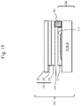
FIG. 15 shows a twelfth embodiment according to the present invention.
FIG. 15 shows a modified embodiment to the embodiment of FIG. 13A with a different position of the third spacer S3. The third spacer S3 is configured between the top stack TS and the bottom stack BS of the force sensor FS. The four gap G4 is configured between the top stack TS and the bottom stack BS. The third spacer S3 has a top end connected to the top piezo layer 22 and has a bottom end connected to the printed circuit board 26. The top stack TS is cantilevered from the bottom stack BS.
FIG. 16 shows a thirteenth embodiment according to the present invention.
FIG. 16 shows a modified embodiment to the embodiment of FIG. 13A with a different position of the third spacer S3. The third spacer S3 is configured between the top stack TS and the bottom stack BS and configured in the right side of the force sensor FS. The four gap G4 is configured between the top stack TS and the bottom stack BS. The third spacer S3 has a top end connected to the top substrate 20 of the top stack TS and has a bottom end connected to the bottom piezo layer 23 of the bottom stack BS. The top stack TS is cantilevered from the bottom stack BS.
FIG. 17 shows a fourteenth embodiment according to the present invention.
FIG. 17 shows that a force sensor 30 is configured with a bottom switch SW. A first conductive contact C1 is configured on the bottom side of the force sensor 30. A second conductive contact C2, aligned with the first conductive contact C1, is configured on a top side of a printed circuit board 26. The force sensor 30 with the first conductive contact and the printed circuit board 26 with the second conductive contact C2 forming the bottom switch SW. The first conductive contact C1 is configured in one of the two states:
(1) slightly touching the second conductive contact C2 without turning on the bottom switch SW, and
(2) slightly apart from touching the second conductive contact, and
a fourth spacer S4 is configured between the force sensor 30 and the printed circuit board 26 and configured in the right side of the force sensor 30. When the force sensor 30 is depressed from the top side, the left side of the force sensor 30 moves down so that the first conductive contact C1 touches the second conductive contact C2 firmly to turn on the bottom switch SW.
The piezo layers 22, 23 disclosed in this invention is made of a material selected from the group consisting of piezo-electric material, triboelectric material, resistive material, and dielectric material
While several embodiments have been described by way of example, it will be apparent to those skilled in the art that various modifications may be configured without departs from the spirit of the present invention. Such modifications are all within the scope of the present invention, as defined by the appended claims.
REFERENCE NUMBERS
  • 20 top substrate
  • 21 top electrode
  • 21B auxiliary metal
  • 22 top piezo layer
  • 23 bottom piezo layer
  • 24 bottom electrode
  • 241, 242 coplanar electrodes
  • 25 bottom substrate
  • 26 printed circuit board
  • 30 force sensor
  • 61 pen tip
  • G1 first gap
  • G2 second gap
  • G3 third gap
  • G4 fourth gap
  • C1 first conductive contact
  • C2 second conductive contact
  • C3 third conductive contact
  • S1 first spacer
  • S2 second spacer
  • S3 third spacer
  • S4 fourth spacer
  • SW switch

Claims (20)

What is claimed is:
1. A cantilever force sensor, comprising a top stack, a bottom stack, and a first spacer, wherein
the first spacer is configured, in a thickness direction of the force sensor, between the top stack and the bottom stack, and is configured in a first side of the force sensor,
a second side, opposite to the first side, of the top stack, is cantilevered from the bottom stack,
in response to the top stack being depressed toward the bottom stack, the second side of the top stack moves down using the first spacer as a fulcrum,
one of the top stack and the bottom stack is a first stack,
another of the top stack and the bottom stack is a second stack,
the first stack comprises:
a first substrate,
a first piezo layer, and
a first electrode between the first substrate and the first piezo layer in the thickness direction, and
along the thickness direction, all of the first substrate, the first electrode and the first piezo layer overlap the first spacer.
2. The cantilever force sensor as claimed in claim 1, wherein
the second stack comprises:
a second substrate,
a second piezo layer, and
a second electrode between the second substrate and the second piezo layer in the thickness direction, and
along the thickness direction, all of the second substrate, the second electrode and the second piezo layer overlap the first spacer.
3. The cantilever force sensor as claimed in claim 1, wherein
the second stack comprises a second substrate and a second electrode stacked over each other in the thickness direction, and
in response to the top stack being depressed toward the bottom stack, the second side of the top stack moves down using the first spacer as a fulcrum and causes the second electrode to come into direct contact with the first piezo layer.
4. The cantilever force sensor as claimed in claim 3, wherein
along the thickness direction, both the second substrate and the second electrode overlap the first spacer.
5. The cantilever force sensor as claimed in claim 1, wherein
the first stack is the bottom stack,
the bottom stack comprises a pair of coplanar electrodes including the first electrode and a second electrode, and
along the thickness direction,
the first piezo layer overlaps both the first and second electrodes, and
the second electrode overlaps the first spacer.
6. The cantilever force sensor as claimed in claim 5, wherein
the top stack comprises a second substrate and an auxiliary metal stacked over each other in the thickness direction, and
in response to the top stack being depressed toward the bottom stack, the second side of the top stack moves down using the first spacer as a fulcrum and causes the auxiliary metal to come into direct contact with the first piezo layer.
7. The cantilever force sensor as claimed in claim 1, further comprising:
a bottom switch, wherein which comprises:
a first conductive contact configured on a bottom side of the bottom stack;
a second conductive contact aligned with the first conductive contact, and configured on a top side of a printed circuit board; and
a second spacer configured between the bottom stack and the printed circuit board in the thickness direction, and configured in the first side of the force sensor.
8. The cantilever force sensor as claimed in claim 7, wherein
in a state where the top stack is not depressed toward the bottom stack, the first conductive contact slightly touches the second conductive contact without turning on the bottom switch.
9. The cantilever force sensor as claimed in claim 7, wherein
in a state where the top stack is not depressed toward the bottom stack, the first conductive contact is slightly apart from the second conductive contact, and
in response to the top stack being depressed toward the bottom stack, a second side opposite to the first side of the bottom stack moves down using the second spacer as a fulcrum and causes the first conductive contact to touch the second conductive contact firmly to turn on the bottom switch.
10. The cantilever force sensor as claimed in claim 1, wherein
the bottom stack comprises a printed circuit board.
11. The cantilever force sensor as claimed in claim 1, wherein
the first piezo layer is made of a material selected from the group consisting of piezo-electric material, triboelectric material, resistive material, and dielectric material.
12. The cantilever force sensor as claimed in claim 1, wherein
the second stack comprises:
a second substrate,
a second piezo layer, and
a second electrode between the second substrate and the second piezo layer in the thickness direction, and
along the thickness direction, the first spacer overlaps the second substrate, without overlapping the second electrode and the second piezo layer.
13. The cantilever force sensor as claimed in claim 12, wherein
the first stack is the top stack,
the second stack is the bottom stack, and
the second substrate is a printed circuit board.
14. A cantilever force sensor, comprising a top stack, a bottom stack, and a spacer, wherein
the spacer is configured, in a thickness direction of the force sensor, between the top stack and the bottom stack, and is configured in a first side of the force sensor,
a second side, opposite to the first side, of the top stack, is cantilevered from the bottom stack,
one of the top stack and the bottom stack is a first stack,
another of the top stack and the bottom stack is a second stack,
the first stack comprises a first substrate and a first electrode stacked over each other in the thickness direction,
the second stack comprises a second substrate and a piezo layer stacked over each other in the thickness direction, and
in response to the top stack being depressed toward the bottom stack, the second side of the top stack moves down using the spacer as a fulcrum and causes the first electrode to come into direct contact with the piezo layer.
15. The cantilever force sensor as claimed in claim 14, wherein
the first stack is the bottom stack,
the bottom stack comprises is a pair of coplanar electrodes including the first electrode and a second electrode, and
in response to the top stack being depressed toward the bottom stack, the second side of the top stack moves down using the first spacer as a fulcrum and causes the piezo layer to come into direct contact with both of the first electrode and the second electrode.
16. The cantilever force sensor as claimed in claim 15, wherein
the second stack is the top stack which further comprises an auxiliary metal between the second substrate and the piezo layer in the thickness direction.
17. The cantilever force sensor as claimed in claim 14, wherein
the second stack further comprises a second electrode between the second substrate and the piezo layer in the thickness direction.
18. The cantilever force sensor as claimed in claim 14, wherein
along the thickness direction, all of the first substrate, the second substrate, the first electrode and the piezo layer overlap the spacer.
19. A cantilever force sensor, comprising a top stack, a bottom stack, and a spacer, wherein
the spacer is configured, in a thickness direction of the force sensor, between the top stack and the bottom stack, and is configured in a first side of the force sensor,
a second side, opposite to the first side, of the top stack, is cantilevered from the bottom stack,
in response to the top stack being depressed toward the bottom stack, the second side of the top stack moves down using the spacer as a fulcrum,
the top stack comprises:
a top substrate,
a top piezo layer, and
a top electrode between the top substrate and the top piezo layer in the thickness direction,
the bottom stack comprises:
a bottom substrate,
a bottom piezo layer, and
a bottom electrode between the bottom substrate and the bottom piezo layer in the thickness direction, and
along the thickness direction, the spacer overlaps the top substrate, the bottom piezo layer and the bottom substrate, without overlapping the top electrode, the top piezo layer and the bottom electrode.
20. The cantilever force sensor as claimed in claim 19, wherein the bottom substrate is a printed circuit board.
US17/152,668 2021-01-19 2021-01-19 Cantilever force sensor Active 2041-04-18 US11609130B2 (en)

Priority Applications (3)

Application Number Priority Date Filing Date Title
US17/152,668 US11609130B2 (en) 2021-01-19 2021-01-19 Cantilever force sensor
CN202110432914.5A CN114812880A (en) 2021-01-19 2021-04-22 Cantilever force sensor
US18/162,719 US20230168138A1 (en) 2021-01-19 2023-02-01 Cantilever force sensor

Applications Claiming Priority (1)

Application Number Priority Date Filing Date Title
US17/152,668 US11609130B2 (en) 2021-01-19 2021-01-19 Cantilever force sensor

Related Child Applications (1)

Application Number Title Priority Date Filing Date
US18/162,719 Continuation US20230168138A1 (en) 2021-01-19 2023-02-01 Cantilever force sensor

Publications (2)

Publication Number Publication Date
US20220228931A1 US20220228931A1 (en) 2022-07-21
US11609130B2 true US11609130B2 (en) 2023-03-21

Family

ID=82405046

Family Applications (2)

Application Number Title Priority Date Filing Date
US17/152,668 Active 2041-04-18 US11609130B2 (en) 2021-01-19 2021-01-19 Cantilever force sensor
US18/162,719 Pending US20230168138A1 (en) 2021-01-19 2023-02-01 Cantilever force sensor

Family Applications After (1)

Application Number Title Priority Date Filing Date
US18/162,719 Pending US20230168138A1 (en) 2021-01-19 2023-02-01 Cantilever force sensor

Country Status (2)

Country Link
US (2) US11609130B2 (en)
CN (1) CN114812880A (en)

Citations (50)

* Cited by examiner, † Cited by third party
Publication number Priority date Publication date Assignee Title
US4398342A (en) * 1981-04-14 1983-08-16 International Standard Electric Corporation Method of making a Hall effect device
US5138879A (en) * 1989-01-04 1992-08-18 Zellweger Uster, Inc. Method for producing multiple fiber data
US5203206A (en) * 1989-01-04 1993-04-20 Zellweger Uster, Inc. Apparatus and methods for testing tension-elongation or cross-sectional properties of single fibers and multiple fiber bundles
US5411919A (en) * 1992-11-17 1995-05-02 Sumitomo Electric Industries, Ltd. Semiconductor device and method of manufacturing the same
US6121870A (en) * 1998-07-28 2000-09-19 Denso Corporation Pressure sensitive transducer with pressure sensitive layer including semi-conductive particles
US20020140533A1 (en) * 1999-07-01 2002-10-03 Masaru Miyazaki Method of producing an integrated type microswitch
US6646215B1 (en) * 2001-06-29 2003-11-11 Teravicin Technologies, Inc. Device adapted to pull a cantilever away from a contact structure
US6825428B1 (en) * 2003-12-16 2004-11-30 Intel Corporation Protected switch and techniques to manufacture the same
US6842097B2 (en) * 2001-03-12 2005-01-11 Hrl Laboratories, Llc Torsion spring for electro-mechanical switches and a cantilever-type RF micro-electromechanical switch incorporating the torsion spring
US6946315B2 (en) * 2001-12-26 2005-09-20 Sony Corporation Manufacturing methods of MEMS device
US7053736B2 (en) * 2002-09-30 2006-05-30 Teravicta Technologies, Inc. Microelectromechanical device having an active opening switch
US20070024403A1 (en) * 2005-07-27 2007-02-01 Samsung Electronics Co., Ltd. MEMS switch actuated by the electrostatic force and piezoelectric force
US7242273B2 (en) * 2003-11-10 2007-07-10 Hitachi Media Electronics Co., Ltd. RF-MEMS switch and its fabrication method
US7501920B2 (en) * 2004-12-21 2009-03-10 Fujitsu Component Limited Switch device
US7623007B2 (en) * 2005-10-19 2009-11-24 Panasonic Corporation Device including piezoelectric thin film and a support having a vertical cross-section with a curvature
US7726175B2 (en) * 2002-06-03 2010-06-01 Arizona Board Of Regents, A Body Corporate Of The State Of Arizona, Acting For Northern Arizona University Embedded piezoelectric microcantilever sensors
US7781687B2 (en) * 2006-09-28 2010-08-24 Siemens Aktiengesellschaft Control unit with a monitoring apparatus
US7785912B2 (en) * 2002-04-23 2010-08-31 Sharp Laboratories Of America, Inc. Piezo-TFT cantilever MEMS fabrication
US7977587B2 (en) * 2008-10-08 2011-07-12 Research In Motion Limited Two-stage switch assembly
US20120050335A1 (en) * 2010-08-25 2012-03-01 Universal Cement Corporation Zooming system for a display
US8217738B2 (en) * 2007-05-17 2012-07-10 Panasonic Corporation Electromechanical element, driving method of the electromechanical element and electronic equipment provided with the same
US8289674B2 (en) * 2009-03-17 2012-10-16 Cavendish Kinetics, Ltd. Moving a free-standing structure between high and low adhesion states
US20120293491A1 (en) * 2011-05-20 2012-11-22 National Tsing Hua University 3-d touch sensor and 3-d touch panel
US8371174B2 (en) 2009-08-31 2013-02-12 Universal Cement Corporation Micro-deformable piezoresistive material and manufacturing method thereof and pressure sensor using the same
US8748997B2 (en) * 2008-12-16 2014-06-10 Samsung Electronics Co., Ltd. Contact-force sensor package and method of fabricating the same
US8779315B2 (en) * 2011-06-02 2014-07-15 Universal Cement Corporation Cover glass pressure button
US8993913B2 (en) * 2011-06-02 2015-03-31 Universal Cement Corporation Cover glass pressure button
US9070499B2 (en) * 2013-05-14 2015-06-30 Universal Cement Corporation Light emitting key
US20160054184A1 (en) * 2014-08-22 2016-02-25 Uneo Inc. Instant response pressure sensor
US9324515B2 (en) * 2012-08-06 2016-04-26 Synaptics Incorporated Touchsurface assembly utilizing magnetically enabled hinge
US9335840B1 (en) * 2014-11-21 2016-05-10 Uneo Inc. Flexible circuit board based force sensor
US9679713B2 (en) * 2015-05-26 2017-06-13 Uneo Incorporated Key switch and analog pressure detection system including the same
US9762236B2 (en) * 2015-02-02 2017-09-12 Uneo Inc. Embedded button for an electronic device
US9766725B2 (en) * 2015-04-22 2017-09-19 Uneo Inc. Force sensing module
US20170283249A1 (en) * 2016-04-01 2017-10-05 Intel Corporation Piezoelectric package-integrated switching devices
US10088937B2 (en) * 2012-05-03 2018-10-02 Apple Inc. Touch input device including a moment compensated bending sensor for load measurement on platform supported by bending beams
US10234339B2 (en) * 2016-06-02 2019-03-19 Uneo Inc. Force sensor with noise shielding layer
US10365737B2 (en) * 2016-01-29 2019-07-30 Hyundai Motor Company Touch input device
US10394379B2 (en) * 2016-01-29 2019-08-27 Hyundai Motor Company Touch input device
US10409391B2 (en) * 2015-09-30 2019-09-10 Apple Inc. Keyboard with adaptive input row
US10423253B2 (en) * 2017-04-20 2019-09-24 Htc Corporation Handheld electronic apparatus, touch sensor and touch detection method thereof
US10429254B2 (en) * 2017-04-27 2019-10-01 Universal Cement Corporation Piezo force sensor with solid-state bonding spacer
US10578499B2 (en) * 2013-02-17 2020-03-03 Microsoft Technology Licensing, Llc Piezo-actuated virtual buttons for touch surfaces
US10825628B2 (en) * 2017-07-17 2020-11-03 Analog Devices Global Unlimited Company Electromagnetically actuated microelectromechanical switch
US20200348757A1 (en) * 2019-05-03 2020-11-05 Immersion Corporation Force sensors for haptic surfaces
US10852319B2 (en) * 2017-06-29 2020-12-01 Infineon Technologies Dresden GmbH & Co. KG Micromechanical sensor and methods for producing a micromechanical sensor and a micromechanical sensor element
US10866260B2 (en) * 2017-03-24 2020-12-15 Seiko Epson Corporation Physical quantity sensor, electronic apparatus, and vehicle
US10874475B2 (en) * 2015-11-12 2020-12-29 Covidien Lp Robotic surgical systems and methods for monitoring applied forces
US11150734B2 (en) * 2016-09-21 2021-10-19 Apple Inc. Haptic structure for providing localized haptic output
US11366493B2 (en) * 2015-09-30 2022-06-21 Apple Inc. Input devices incorporating biometric sensors

Patent Citations (51)

* Cited by examiner, † Cited by third party
Publication number Priority date Publication date Assignee Title
US4398342A (en) * 1981-04-14 1983-08-16 International Standard Electric Corporation Method of making a Hall effect device
US5138879A (en) * 1989-01-04 1992-08-18 Zellweger Uster, Inc. Method for producing multiple fiber data
US5203206A (en) * 1989-01-04 1993-04-20 Zellweger Uster, Inc. Apparatus and methods for testing tension-elongation or cross-sectional properties of single fibers and multiple fiber bundles
US5411919A (en) * 1992-11-17 1995-05-02 Sumitomo Electric Industries, Ltd. Semiconductor device and method of manufacturing the same
US6121870A (en) * 1998-07-28 2000-09-19 Denso Corporation Pressure sensitive transducer with pressure sensitive layer including semi-conductive particles
US20020140533A1 (en) * 1999-07-01 2002-10-03 Masaru Miyazaki Method of producing an integrated type microswitch
US6842097B2 (en) * 2001-03-12 2005-01-11 Hrl Laboratories, Llc Torsion spring for electro-mechanical switches and a cantilever-type RF micro-electromechanical switch incorporating the torsion spring
US6646215B1 (en) * 2001-06-29 2003-11-11 Teravicin Technologies, Inc. Device adapted to pull a cantilever away from a contact structure
US6946315B2 (en) * 2001-12-26 2005-09-20 Sony Corporation Manufacturing methods of MEMS device
US7785912B2 (en) * 2002-04-23 2010-08-31 Sharp Laboratories Of America, Inc. Piezo-TFT cantilever MEMS fabrication
US7726175B2 (en) * 2002-06-03 2010-06-01 Arizona Board Of Regents, A Body Corporate Of The State Of Arizona, Acting For Northern Arizona University Embedded piezoelectric microcantilever sensors
US7053736B2 (en) * 2002-09-30 2006-05-30 Teravicta Technologies, Inc. Microelectromechanical device having an active opening switch
US7242273B2 (en) * 2003-11-10 2007-07-10 Hitachi Media Electronics Co., Ltd. RF-MEMS switch and its fabrication method
US6825428B1 (en) * 2003-12-16 2004-11-30 Intel Corporation Protected switch and techniques to manufacture the same
US7501920B2 (en) * 2004-12-21 2009-03-10 Fujitsu Component Limited Switch device
US20070024403A1 (en) * 2005-07-27 2007-02-01 Samsung Electronics Co., Ltd. MEMS switch actuated by the electrostatic force and piezoelectric force
US7623007B2 (en) * 2005-10-19 2009-11-24 Panasonic Corporation Device including piezoelectric thin film and a support having a vertical cross-section with a curvature
US7781687B2 (en) * 2006-09-28 2010-08-24 Siemens Aktiengesellschaft Control unit with a monitoring apparatus
US8217738B2 (en) * 2007-05-17 2012-07-10 Panasonic Corporation Electromechanical element, driving method of the electromechanical element and electronic equipment provided with the same
US7977587B2 (en) * 2008-10-08 2011-07-12 Research In Motion Limited Two-stage switch assembly
US8748997B2 (en) * 2008-12-16 2014-06-10 Samsung Electronics Co., Ltd. Contact-force sensor package and method of fabricating the same
US8289674B2 (en) * 2009-03-17 2012-10-16 Cavendish Kinetics, Ltd. Moving a free-standing structure between high and low adhesion states
US8371174B2 (en) 2009-08-31 2013-02-12 Universal Cement Corporation Micro-deformable piezoresistive material and manufacturing method thereof and pressure sensor using the same
US20120050335A1 (en) * 2010-08-25 2012-03-01 Universal Cement Corporation Zooming system for a display
US20120293491A1 (en) * 2011-05-20 2012-11-22 National Tsing Hua University 3-d touch sensor and 3-d touch panel
US8779315B2 (en) * 2011-06-02 2014-07-15 Universal Cement Corporation Cover glass pressure button
US8993913B2 (en) * 2011-06-02 2015-03-31 Universal Cement Corporation Cover glass pressure button
US10088937B2 (en) * 2012-05-03 2018-10-02 Apple Inc. Touch input device including a moment compensated bending sensor for load measurement on platform supported by bending beams
US9324515B2 (en) * 2012-08-06 2016-04-26 Synaptics Incorporated Touchsurface assembly utilizing magnetically enabled hinge
US10578499B2 (en) * 2013-02-17 2020-03-03 Microsoft Technology Licensing, Llc Piezo-actuated virtual buttons for touch surfaces
US9070499B2 (en) * 2013-05-14 2015-06-30 Universal Cement Corporation Light emitting key
US20160054184A1 (en) * 2014-08-22 2016-02-25 Uneo Inc. Instant response pressure sensor
US9677954B2 (en) * 2014-08-22 2017-06-13 Uneo Inc. Instant response pressure sensor
US9335840B1 (en) * 2014-11-21 2016-05-10 Uneo Inc. Flexible circuit board based force sensor
US9762236B2 (en) * 2015-02-02 2017-09-12 Uneo Inc. Embedded button for an electronic device
US9766725B2 (en) * 2015-04-22 2017-09-19 Uneo Inc. Force sensing module
US9679713B2 (en) * 2015-05-26 2017-06-13 Uneo Incorporated Key switch and analog pressure detection system including the same
US10409391B2 (en) * 2015-09-30 2019-09-10 Apple Inc. Keyboard with adaptive input row
US11366493B2 (en) * 2015-09-30 2022-06-21 Apple Inc. Input devices incorporating biometric sensors
US10874475B2 (en) * 2015-11-12 2020-12-29 Covidien Lp Robotic surgical systems and methods for monitoring applied forces
US10365737B2 (en) * 2016-01-29 2019-07-30 Hyundai Motor Company Touch input device
US10394379B2 (en) * 2016-01-29 2019-08-27 Hyundai Motor Company Touch input device
US20170283249A1 (en) * 2016-04-01 2017-10-05 Intel Corporation Piezoelectric package-integrated switching devices
US10234339B2 (en) * 2016-06-02 2019-03-19 Uneo Inc. Force sensor with noise shielding layer
US11150734B2 (en) * 2016-09-21 2021-10-19 Apple Inc. Haptic structure for providing localized haptic output
US10866260B2 (en) * 2017-03-24 2020-12-15 Seiko Epson Corporation Physical quantity sensor, electronic apparatus, and vehicle
US10423253B2 (en) * 2017-04-20 2019-09-24 Htc Corporation Handheld electronic apparatus, touch sensor and touch detection method thereof
US10429254B2 (en) * 2017-04-27 2019-10-01 Universal Cement Corporation Piezo force sensor with solid-state bonding spacer
US10852319B2 (en) * 2017-06-29 2020-12-01 Infineon Technologies Dresden GmbH & Co. KG Micromechanical sensor and methods for producing a micromechanical sensor and a micromechanical sensor element
US10825628B2 (en) * 2017-07-17 2020-11-03 Analog Devices Global Unlimited Company Electromagnetically actuated microelectromechanical switch
US20200348757A1 (en) * 2019-05-03 2020-11-05 Immersion Corporation Force sensors for haptic surfaces

Also Published As

Publication number Publication date
US20220228931A1 (en) 2022-07-21
CN114812880A (en) 2022-07-29
US20230168138A1 (en) 2023-06-01

Similar Documents

Publication Publication Date Title
US10042455B2 (en) Detecting sensor having position detection and pressing force detection electrodes
JP4260406B2 (en) Pressing direction detection sensor and input device using the same
JP2011014280A (en) Touch sensor
CN104350566A (en) Input device
US10268301B2 (en) Three-dimensional touch panel
US9677954B2 (en) Instant response pressure sensor
US11157125B2 (en) Touch panel implementing touch and pressure sensing performances and related touch display panel
JP2008282724A (en) Switch device
US9959001B2 (en) Touch substrate, method for manufacturing the same and touch device
US11609130B2 (en) Cantilever force sensor
JP2002107245A (en) Force detector
JPH07160396A (en) Pointing device
US8681117B2 (en) Flexible slide-touch controlling device and the related position determination method
JP2002131149A (en) Force detecting device
US11487422B2 (en) Force sensing dome switch
US8618431B2 (en) Touch sensing unit and method for manufacturing the same
JPH10149737A (en) Membrane switch
US11621710B2 (en) Capacitance switch
JP7395114B2 (en) Membrane switch that can detect pressure and its manufacturing method
JPH0448600Y2 (en)
KR200236088Y1 (en) Touch panel assembly
JPS6146512A (en) Pen for input device
JP3451362B2 (en) Capacitive sensor
WO2018207486A1 (en) Shift device
KR20080078144A (en) Capacitive input device

Legal Events

Date Code Title Description
FEPP Fee payment procedure

Free format text: ENTITY STATUS SET TO UNDISCOUNTED (ORIGINAL EVENT CODE: BIG.); ENTITY STATUS OF PATENT OWNER: SMALL ENTITY

AS Assignment

Owner name: UNEO INC., TAIWAN

Free format text: ASSIGNMENT OF ASSIGNORS INTEREST;ASSIGNORS:HOU, CHIH-SHENG;CHOU, CHIA-HUNG;SIGNING DATES FROM 20210115 TO 20210118;REEL/FRAME:054967/0758

FEPP Fee payment procedure

Free format text: ENTITY STATUS SET TO SMALL (ORIGINAL EVENT CODE: SMAL); ENTITY STATUS OF PATENT OWNER: SMALL ENTITY

STPP Information on status: patent application and granting procedure in general

Free format text: NON FINAL ACTION MAILED

STPP Information on status: patent application and granting procedure in general

Free format text: RESPONSE TO NON-FINAL OFFICE ACTION ENTERED AND FORWARDED TO EXAMINER

STPP Information on status: patent application and granting procedure in general

Free format text: NOTICE OF ALLOWANCE MAILED -- APPLICATION RECEIVED IN OFFICE OF PUBLICATIONS

STPP Information on status: patent application and granting procedure in general

Free format text: NOTICE OF ALLOWANCE MAILED -- APPLICATION RECEIVED IN OFFICE OF PUBLICATIONS

STCF Information on status: patent grant

Free format text: PATENTED CASE