US11545404B2 - III-V compound semiconductor dies with stress-treated inactive surfaces to avoid packaging-induced fractures, and related methods - Google Patents
III-V compound semiconductor dies with stress-treated inactive surfaces to avoid packaging-induced fractures, and related methods Download PDFInfo
- Publication number
- US11545404B2 US11545404B2 US16/868,147 US202016868147A US11545404B2 US 11545404 B2 US11545404 B2 US 11545404B2 US 202016868147 A US202016868147 A US 202016868147A US 11545404 B2 US11545404 B2 US 11545404B2
- Authority
- US
- United States
- Prior art keywords
- iii
- compound
- chip package
- die
- substrate
- Prior art date
- Legal status (The legal status is an assumption and is not a legal conclusion. Google has not performed a legal analysis and makes no representation as to the accuracy of the status listed.)
- Active
Links
- 150000001875 compounds Chemical class 0.000 title claims abstract description 234
- 239000004065 semiconductor Substances 0.000 title claims abstract description 153
- 238000000034 method Methods 0.000 title description 50
- 238000004806 packaging method and process Methods 0.000 title description 8
- 238000002161 passivation Methods 0.000 claims abstract description 97
- 239000000758 substrate Substances 0.000 claims abstract description 82
- 238000000465 moulding Methods 0.000 claims abstract description 53
- 239000000463 material Substances 0.000 claims abstract description 21
- 230000006854 communication Effects 0.000 claims description 12
- 238000004891 communication Methods 0.000 claims description 12
- 230000008878 coupling Effects 0.000 claims description 7
- 238000010168 coupling process Methods 0.000 claims description 7
- 238000005859 coupling reaction Methods 0.000 claims description 7
- 229910052581 Si3N4 Inorganic materials 0.000 claims description 6
- HQVNEWCFYHHQES-UHFFFAOYSA-N silicon nitride Chemical compound N12[Si]34N5[Si]62N3[Si]51N64 HQVNEWCFYHHQES-UHFFFAOYSA-N 0.000 claims description 6
- JBRZTFJDHDCESZ-UHFFFAOYSA-N AsGa Chemical compound [As]#[Ga] JBRZTFJDHDCESZ-UHFFFAOYSA-N 0.000 claims description 5
- 229910000413 arsenic oxide Inorganic materials 0.000 claims description 3
- IKWTVSLWAPBBKU-UHFFFAOYSA-N a1010_sial Chemical compound O=[As]O[As]=O IKWTVSLWAPBBKU-UHFFFAOYSA-N 0.000 claims description 2
- 229960002594 arsenic trioxide Drugs 0.000 claims description 2
- 230000001413 cellular effect Effects 0.000 claims description 2
- AJNVQOSZGJRYEI-UHFFFAOYSA-N digallium;oxygen(2-) Chemical compound [O-2].[O-2].[O-2].[Ga+3].[Ga+3] AJNVQOSZGJRYEI-UHFFFAOYSA-N 0.000 claims description 2
- 230000000977 initiatory effect Effects 0.000 claims description 2
- LIVNPJMFVYWSIS-UHFFFAOYSA-N silicon monoxide Chemical compound [Si-]#[O+] LIVNPJMFVYWSIS-UHFFFAOYSA-N 0.000 claims description 2
- KTTMEOWBIWLMSE-UHFFFAOYSA-N diarsenic trioxide Chemical compound O1[As](O2)O[As]3O[As]1O[As]2O3 KTTMEOWBIWLMSE-UHFFFAOYSA-N 0.000 claims 1
- 238000004519 manufacturing process Methods 0.000 abstract description 31
- 230000001902 propagating effect Effects 0.000 abstract description 10
- 239000013078 crystal Substances 0.000 abstract description 5
- 239000010410 layer Substances 0.000 description 102
- 235000012431 wafers Nutrition 0.000 description 54
- 230000008569 process Effects 0.000 description 18
- 239000011241 protective layer Substances 0.000 description 16
- 238000005538 encapsulation Methods 0.000 description 13
- 230000003647 oxidation Effects 0.000 description 11
- 238000007254 oxidation reaction Methods 0.000 description 11
- XUIMIQQOPSSXEZ-UHFFFAOYSA-N Silicon Chemical compound [Si] XUIMIQQOPSSXEZ-UHFFFAOYSA-N 0.000 description 8
- QVGXLLKOCUKJST-UHFFFAOYSA-N atomic oxygen Chemical compound [O] QVGXLLKOCUKJST-UHFFFAOYSA-N 0.000 description 8
- 229910052760 oxygen Inorganic materials 0.000 description 8
- 239000001301 oxygen Substances 0.000 description 8
- 229910052710 silicon Inorganic materials 0.000 description 8
- 239000010703 silicon Substances 0.000 description 8
- 238000000151 deposition Methods 0.000 description 7
- 238000012545 processing Methods 0.000 description 6
- 229910045601 alloy Inorganic materials 0.000 description 5
- 239000000956 alloy Substances 0.000 description 5
- 238000006243 chemical reaction Methods 0.000 description 5
- 238000003860 storage Methods 0.000 description 5
- 230000000737 periodic effect Effects 0.000 description 4
- 238000013461 design Methods 0.000 description 3
- 238000010586 diagram Methods 0.000 description 3
- 229910000679 solder Inorganic materials 0.000 description 3
- 239000002344 surface layer Substances 0.000 description 3
- GOLCXWYRSKYTSP-UHFFFAOYSA-N Arsenious Acid Chemical compound O1[As]2O[As]1O2 GOLCXWYRSKYTSP-UHFFFAOYSA-N 0.000 description 2
- VYPSYNLAJGMNEJ-UHFFFAOYSA-N Silicium dioxide Chemical compound O=[Si]=O VYPSYNLAJGMNEJ-UHFFFAOYSA-N 0.000 description 2
- -1 accelerators Substances 0.000 description 2
- 238000005516 engineering process Methods 0.000 description 2
- 238000012986 modification Methods 0.000 description 2
- 230000004048 modification Effects 0.000 description 2
- 239000002245 particle Substances 0.000 description 2
- 238000007493 shaping process Methods 0.000 description 2
- 229910052814 silicon oxide Inorganic materials 0.000 description 2
- XLYOFNOQVPJJNP-UHFFFAOYSA-N water Substances O XLYOFNOQVPJJNP-UHFFFAOYSA-N 0.000 description 2
- 239000004593 Epoxy Substances 0.000 description 1
- 229910001218 Gallium arsenide Inorganic materials 0.000 description 1
- 239000002318 adhesion promoter Substances 0.000 description 1
- 238000003491 array Methods 0.000 description 1
- 230000007175 bidirectional communication Effects 0.000 description 1
- 239000003054 catalyst Substances 0.000 description 1
- 230000008859 change Effects 0.000 description 1
- 239000003795 chemical substances by application Substances 0.000 description 1
- 238000005229 chemical vapour deposition Methods 0.000 description 1
- 239000002131 composite material Substances 0.000 description 1
- 230000008602 contraction Effects 0.000 description 1
- 238000005336 cracking Methods 0.000 description 1
- 238000005520 cutting process Methods 0.000 description 1
- 230000001627 detrimental effect Effects 0.000 description 1
- 230000007613 environmental effect Effects 0.000 description 1
- 239000003822 epoxy resin Substances 0.000 description 1
- 239000004744 fabric Substances 0.000 description 1
- 239000000945 filler Substances 0.000 description 1
- 239000003063 flame retardant Substances 0.000 description 1
- 230000006870 function Effects 0.000 description 1
- LNEPOXFFQSENCJ-UHFFFAOYSA-N haloperidol Chemical compound C1CC(O)(C=2C=CC(Cl)=CC=2)CCN1CCCC(=O)C1=CC=C(F)C=C1 LNEPOXFFQSENCJ-UHFFFAOYSA-N 0.000 description 1
- 230000036541 health Effects 0.000 description 1
- 239000004973 liquid crystal related substance Substances 0.000 description 1
- 229910052751 metal Inorganic materials 0.000 description 1
- 239000002184 metal Substances 0.000 description 1
- 150000002739 metals Chemical class 0.000 description 1
- 239000000203 mixture Substances 0.000 description 1
- 239000006082 mold release agent Substances 0.000 description 1
- 230000003287 optical effect Effects 0.000 description 1
- 230000005693 optoelectronics Effects 0.000 description 1
- 230000001590 oxidative effect Effects 0.000 description 1
- 238000012536 packaging technology Methods 0.000 description 1
- ISWSIDIOOBJBQZ-UHFFFAOYSA-N phenol group Chemical group C1(=CC=CC=C1)O ISWSIDIOOBJBQZ-UHFFFAOYSA-N 0.000 description 1
- 239000000049 pigment Substances 0.000 description 1
- 229920000647 polyepoxide Polymers 0.000 description 1
- 239000004848 polyfunctional curative Substances 0.000 description 1
- 238000009877 rendering Methods 0.000 description 1
- 230000004044 response Effects 0.000 description 1
- 238000006748 scratching Methods 0.000 description 1
- 230000002393 scratching effect Effects 0.000 description 1
- 238000000926 separation method Methods 0.000 description 1
- 230000001131 transforming effect Effects 0.000 description 1
- 230000000007 visual effect Effects 0.000 description 1
- 238000007704 wet chemistry method Methods 0.000 description 1
Images


Classifications
-
- H—ELECTRICITY
- H01—ELECTRIC ELEMENTS
- H01L—SEMICONDUCTOR DEVICES NOT COVERED BY CLASS H10
- H01L23/00—Details of semiconductor or other solid state devices
- H01L23/28—Encapsulations, e.g. encapsulating layers, coatings, e.g. for protection
- H01L23/31—Encapsulations, e.g. encapsulating layers, coatings, e.g. for protection characterised by the arrangement or shape
- H01L23/3107—Encapsulations, e.g. encapsulating layers, coatings, e.g. for protection characterised by the arrangement or shape the device being completely enclosed
- H01L23/3114—Encapsulations, e.g. encapsulating layers, coatings, e.g. for protection characterised by the arrangement or shape the device being completely enclosed the device being a chip scale package, e.g. CSP
-
- H—ELECTRICITY
- H01—ELECTRIC ELEMENTS
- H01L—SEMICONDUCTOR DEVICES NOT COVERED BY CLASS H10
- H01L23/00—Details of semiconductor or other solid state devices
- H01L23/28—Encapsulations, e.g. encapsulating layers, coatings, e.g. for protection
- H01L23/31—Encapsulations, e.g. encapsulating layers, coatings, e.g. for protection characterised by the arrangement or shape
- H01L23/3157—Partial encapsulation or coating
- H01L23/3171—Partial encapsulation or coating the coating being directly applied to the semiconductor body, e.g. passivation layer
-
- H—ELECTRICITY
- H01—ELECTRIC ELEMENTS
- H01L—SEMICONDUCTOR DEVICES NOT COVERED BY CLASS H10
- H01L21/00—Processes or apparatus adapted for the manufacture or treatment of semiconductor or solid state devices or of parts thereof
- H01L21/02—Manufacture or treatment of semiconductor devices or of parts thereof
- H01L21/04—Manufacture or treatment of semiconductor devices or of parts thereof the devices having potential barriers, e.g. a PN junction, depletion layer or carrier concentration layer
- H01L21/50—Assembly of semiconductor devices using processes or apparatus not provided for in a single one of the subgroups H01L21/06 - H01L21/326, e.g. sealing of a cap to a base of a container
- H01L21/56—Encapsulations, e.g. encapsulation layers, coatings
-
- H—ELECTRICITY
- H01—ELECTRIC ELEMENTS
- H01L—SEMICONDUCTOR DEVICES NOT COVERED BY CLASS H10
- H01L21/00—Processes or apparatus adapted for the manufacture or treatment of semiconductor or solid state devices or of parts thereof
- H01L21/67—Apparatus specially adapted for handling semiconductor or electric solid state devices during manufacture or treatment thereof; Apparatus specially adapted for handling wafers during manufacture or treatment of semiconductor or electric solid state devices or components ; Apparatus not specifically provided for elsewhere
- H01L21/683—Apparatus specially adapted for handling semiconductor or electric solid state devices during manufacture or treatment thereof; Apparatus specially adapted for handling wafers during manufacture or treatment of semiconductor or electric solid state devices or components ; Apparatus not specifically provided for elsewhere for supporting or gripping
- H01L21/6835—Apparatus specially adapted for handling semiconductor or electric solid state devices during manufacture or treatment thereof; Apparatus specially adapted for handling wafers during manufacture or treatment of semiconductor or electric solid state devices or components ; Apparatus not specifically provided for elsewhere for supporting or gripping using temporarily an auxiliary support
-
- H—ELECTRICITY
- H01—ELECTRIC ELEMENTS
- H01L—SEMICONDUCTOR DEVICES NOT COVERED BY CLASS H10
- H01L21/00—Processes or apparatus adapted for the manufacture or treatment of semiconductor or solid state devices or of parts thereof
- H01L21/70—Manufacture or treatment of devices consisting of a plurality of solid state components formed in or on a common substrate or of parts thereof; Manufacture of integrated circuit devices or of parts thereof
- H01L21/77—Manufacture or treatment of devices consisting of a plurality of solid state components or integrated circuits formed in, or on, a common substrate
- H01L21/78—Manufacture or treatment of devices consisting of a plurality of solid state components or integrated circuits formed in, or on, a common substrate with subsequent division of the substrate into plural individual devices
-
- H—ELECTRICITY
- H01—ELECTRIC ELEMENTS
- H01L—SEMICONDUCTOR DEVICES NOT COVERED BY CLASS H10
- H01L23/00—Details of semiconductor or other solid state devices
- H01L23/28—Encapsulations, e.g. encapsulating layers, coatings, e.g. for protection
- H01L23/29—Encapsulations, e.g. encapsulating layers, coatings, e.g. for protection characterised by the material, e.g. carbon
- H01L23/291—Oxides or nitrides or carbides, e.g. ceramics, glass
-
- H—ELECTRICITY
- H01—ELECTRIC ELEMENTS
- H01L—SEMICONDUCTOR DEVICES NOT COVERED BY CLASS H10
- H01L23/00—Details of semiconductor or other solid state devices
- H01L23/28—Encapsulations, e.g. encapsulating layers, coatings, e.g. for protection
- H01L23/31—Encapsulations, e.g. encapsulating layers, coatings, e.g. for protection characterised by the arrangement or shape
- H01L23/3107—Encapsulations, e.g. encapsulating layers, coatings, e.g. for protection characterised by the arrangement or shape the device being completely enclosed
- H01L23/3121—Encapsulations, e.g. encapsulating layers, coatings, e.g. for protection characterised by the arrangement or shape the device being completely enclosed a substrate forming part of the encapsulation
-
- H—ELECTRICITY
- H01—ELECTRIC ELEMENTS
- H01L—SEMICONDUCTOR DEVICES NOT COVERED BY CLASS H10
- H01L23/00—Details of semiconductor or other solid state devices
- H01L23/28—Encapsulations, e.g. encapsulating layers, coatings, e.g. for protection
- H01L23/31—Encapsulations, e.g. encapsulating layers, coatings, e.g. for protection characterised by the arrangement or shape
- H01L23/3157—Partial encapsulation or coating
- H01L23/3185—Partial encapsulation or coating the coating covering also the sidewalls of the semiconductor body
-
- H—ELECTRICITY
- H01—ELECTRIC ELEMENTS
- H01L—SEMICONDUCTOR DEVICES NOT COVERED BY CLASS H10
- H01L24/00—Arrangements for connecting or disconnecting semiconductor or solid-state bodies; Methods or apparatus related thereto
- H01L24/01—Means for bonding being attached to, or being formed on, the surface to be connected, e.g. chip-to-package, die-attach, "first-level" interconnects; Manufacturing methods related thereto
- H01L24/10—Bump connectors ; Manufacturing methods related thereto
- H01L24/12—Structure, shape, material or disposition of the bump connectors prior to the connecting process
- H01L24/13—Structure, shape, material or disposition of the bump connectors prior to the connecting process of an individual bump connector
-
- H—ELECTRICITY
- H01—ELECTRIC ELEMENTS
- H01L—SEMICONDUCTOR DEVICES NOT COVERED BY CLASS H10
- H01L24/00—Arrangements for connecting or disconnecting semiconductor or solid-state bodies; Methods or apparatus related thereto
- H01L24/01—Means for bonding being attached to, or being formed on, the surface to be connected, e.g. chip-to-package, die-attach, "first-level" interconnects; Manufacturing methods related thereto
- H01L24/10—Bump connectors ; Manufacturing methods related thereto
- H01L24/15—Structure, shape, material or disposition of the bump connectors after the connecting process
-
- H—ELECTRICITY
- H01—ELECTRIC ELEMENTS
- H01L—SEMICONDUCTOR DEVICES NOT COVERED BY CLASS H10
- H01L24/00—Arrangements for connecting or disconnecting semiconductor or solid-state bodies; Methods or apparatus related thereto
- H01L24/01—Means for bonding being attached to, or being formed on, the surface to be connected, e.g. chip-to-package, die-attach, "first-level" interconnects; Manufacturing methods related thereto
- H01L24/42—Wire connectors; Manufacturing methods related thereto
- H01L24/44—Structure, shape, material or disposition of the wire connectors prior to the connecting process
- H01L24/45—Structure, shape, material or disposition of the wire connectors prior to the connecting process of an individual wire connector
-
- H—ELECTRICITY
- H01—ELECTRIC ELEMENTS
- H01L—SEMICONDUCTOR DEVICES NOT COVERED BY CLASS H10
- H01L24/00—Arrangements for connecting or disconnecting semiconductor or solid-state bodies; Methods or apparatus related thereto
- H01L24/01—Means for bonding being attached to, or being formed on, the surface to be connected, e.g. chip-to-package, die-attach, "first-level" interconnects; Manufacturing methods related thereto
- H01L24/42—Wire connectors; Manufacturing methods related thereto
- H01L24/47—Structure, shape, material or disposition of the wire connectors after the connecting process
-
- H—ELECTRICITY
- H01—ELECTRIC ELEMENTS
- H01L—SEMICONDUCTOR DEVICES NOT COVERED BY CLASS H10
- H01L24/00—Arrangements for connecting or disconnecting semiconductor or solid-state bodies; Methods or apparatus related thereto
- H01L24/80—Methods for connecting semiconductor or other solid state bodies using means for bonding being attached to, or being formed on, the surface to be connected
- H01L24/81—Methods for connecting semiconductor or other solid state bodies using means for bonding being attached to, or being formed on, the surface to be connected using a bump connector
-
- H—ELECTRICITY
- H01—ELECTRIC ELEMENTS
- H01L—SEMICONDUCTOR DEVICES NOT COVERED BY CLASS H10
- H01L24/00—Arrangements for connecting or disconnecting semiconductor or solid-state bodies; Methods or apparatus related thereto
- H01L24/80—Methods for connecting semiconductor or other solid state bodies using means for bonding being attached to, or being formed on, the surface to be connected
- H01L24/85—Methods for connecting semiconductor or other solid state bodies using means for bonding being attached to, or being formed on, the surface to be connected using a wire connector
-
- H—ELECTRICITY
- H01—ELECTRIC ELEMENTS
- H01L—SEMICONDUCTOR DEVICES NOT COVERED BY CLASS H10
- H01L24/00—Arrangements for connecting or disconnecting semiconductor or solid-state bodies; Methods or apparatus related thereto
- H01L24/93—Batch processes
- H01L24/94—Batch processes at wafer-level, i.e. with connecting carried out on a wafer comprising a plurality of undiced individual devices
-
- H—ELECTRICITY
- H01—ELECTRIC ELEMENTS
- H01L—SEMICONDUCTOR DEVICES NOT COVERED BY CLASS H10
- H01L2221/00—Processes or apparatus adapted for the manufacture or treatment of semiconductor or solid state devices or of parts thereof covered by H01L21/00
- H01L2221/67—Apparatus for handling semiconductor or electric solid state devices during manufacture or treatment thereof; Apparatus for handling wafers during manufacture or treatment of semiconductor or electric solid state devices or components; Apparatus not specifically provided for elsewhere
- H01L2221/683—Apparatus for handling semiconductor or electric solid state devices during manufacture or treatment thereof; Apparatus for handling wafers during manufacture or treatment of semiconductor or electric solid state devices or components; Apparatus not specifically provided for elsewhere for supporting or gripping
- H01L2221/68304—Apparatus for handling semiconductor or electric solid state devices during manufacture or treatment thereof; Apparatus for handling wafers during manufacture or treatment of semiconductor or electric solid state devices or components; Apparatus not specifically provided for elsewhere for supporting or gripping using temporarily an auxiliary support
- H01L2221/68327—Apparatus for handling semiconductor or electric solid state devices during manufacture or treatment thereof; Apparatus for handling wafers during manufacture or treatment of semiconductor or electric solid state devices or components; Apparatus not specifically provided for elsewhere for supporting or gripping using temporarily an auxiliary support used during dicing or grinding
-
- H—ELECTRICITY
- H01—ELECTRIC ELEMENTS
- H01L—SEMICONDUCTOR DEVICES NOT COVERED BY CLASS H10
- H01L2221/00—Processes or apparatus adapted for the manufacture or treatment of semiconductor or solid state devices or of parts thereof covered by H01L21/00
- H01L2221/67—Apparatus for handling semiconductor or electric solid state devices during manufacture or treatment thereof; Apparatus for handling wafers during manufacture or treatment of semiconductor or electric solid state devices or components; Apparatus not specifically provided for elsewhere
- H01L2221/683—Apparatus for handling semiconductor or electric solid state devices during manufacture or treatment thereof; Apparatus for handling wafers during manufacture or treatment of semiconductor or electric solid state devices or components; Apparatus not specifically provided for elsewhere for supporting or gripping
- H01L2221/68304—Apparatus for handling semiconductor or electric solid state devices during manufacture or treatment thereof; Apparatus for handling wafers during manufacture or treatment of semiconductor or electric solid state devices or components; Apparatus not specifically provided for elsewhere for supporting or gripping using temporarily an auxiliary support
- H01L2221/6834—Apparatus for handling semiconductor or electric solid state devices during manufacture or treatment thereof; Apparatus for handling wafers during manufacture or treatment of semiconductor or electric solid state devices or components; Apparatus not specifically provided for elsewhere for supporting or gripping using temporarily an auxiliary support used to protect an active side of a device or wafer
-
- H—ELECTRICITY
- H01—ELECTRIC ELEMENTS
- H01L—SEMICONDUCTOR DEVICES NOT COVERED BY CLASS H10
- H01L2221/00—Processes or apparatus adapted for the manufacture or treatment of semiconductor or solid state devices or of parts thereof covered by H01L21/00
- H01L2221/67—Apparatus for handling semiconductor or electric solid state devices during manufacture or treatment thereof; Apparatus for handling wafers during manufacture or treatment of semiconductor or electric solid state devices or components; Apparatus not specifically provided for elsewhere
- H01L2221/683—Apparatus for handling semiconductor or electric solid state devices during manufacture or treatment thereof; Apparatus for handling wafers during manufacture or treatment of semiconductor or electric solid state devices or components; Apparatus not specifically provided for elsewhere for supporting or gripping
- H01L2221/68304—Apparatus for handling semiconductor or electric solid state devices during manufacture or treatment thereof; Apparatus for handling wafers during manufacture or treatment of semiconductor or electric solid state devices or components; Apparatus not specifically provided for elsewhere for supporting or gripping using temporarily an auxiliary support
- H01L2221/68354—Apparatus for handling semiconductor or electric solid state devices during manufacture or treatment thereof; Apparatus for handling wafers during manufacture or treatment of semiconductor or electric solid state devices or components; Apparatus not specifically provided for elsewhere for supporting or gripping using temporarily an auxiliary support used to support diced chips prior to mounting
-
- H—ELECTRICITY
- H01—ELECTRIC ELEMENTS
- H01L—SEMICONDUCTOR DEVICES NOT COVERED BY CLASS H10
- H01L2221/00—Processes or apparatus adapted for the manufacture or treatment of semiconductor or solid state devices or of parts thereof covered by H01L21/00
- H01L2221/67—Apparatus for handling semiconductor or electric solid state devices during manufacture or treatment thereof; Apparatus for handling wafers during manufacture or treatment of semiconductor or electric solid state devices or components; Apparatus not specifically provided for elsewhere
- H01L2221/683—Apparatus for handling semiconductor or electric solid state devices during manufacture or treatment thereof; Apparatus for handling wafers during manufacture or treatment of semiconductor or electric solid state devices or components; Apparatus not specifically provided for elsewhere for supporting or gripping
- H01L2221/68304—Apparatus for handling semiconductor or electric solid state devices during manufacture or treatment thereof; Apparatus for handling wafers during manufacture or treatment of semiconductor or electric solid state devices or components; Apparatus not specifically provided for elsewhere for supporting or gripping using temporarily an auxiliary support
- H01L2221/68368—Apparatus for handling semiconductor or electric solid state devices during manufacture or treatment thereof; Apparatus for handling wafers during manufacture or treatment of semiconductor or electric solid state devices or components; Apparatus not specifically provided for elsewhere for supporting or gripping using temporarily an auxiliary support used in a transfer process involving at least two transfer steps, i.e. including an intermediate handle substrate
-
- H—ELECTRICITY
- H01—ELECTRIC ELEMENTS
- H01L—SEMICONDUCTOR DEVICES NOT COVERED BY CLASS H10
- H01L2224/00—Indexing scheme for arrangements for connecting or disconnecting semiconductor or solid-state bodies and methods related thereto as covered by H01L24/00
- H01L2224/01—Means for bonding being attached to, or being formed on, the surface to be connected, e.g. chip-to-package, die-attach, "first-level" interconnects; Manufacturing methods related thereto
- H01L2224/02—Bonding areas; Manufacturing methods related thereto
- H01L2224/04—Structure, shape, material or disposition of the bonding areas prior to the connecting process
- H01L2224/0401—Bonding areas specifically adapted for bump connectors, e.g. under bump metallisation [UBM]
-
- H—ELECTRICITY
- H01—ELECTRIC ELEMENTS
- H01L—SEMICONDUCTOR DEVICES NOT COVERED BY CLASS H10
- H01L2224/00—Indexing scheme for arrangements for connecting or disconnecting semiconductor or solid-state bodies and methods related thereto as covered by H01L24/00
- H01L2224/01—Means for bonding being attached to, or being formed on, the surface to be connected, e.g. chip-to-package, die-attach, "first-level" interconnects; Manufacturing methods related thereto
- H01L2224/02—Bonding areas; Manufacturing methods related thereto
- H01L2224/04—Structure, shape, material or disposition of the bonding areas prior to the connecting process
- H01L2224/04042—Bonding areas specifically adapted for wire connectors, e.g. wirebond pads
-
- H—ELECTRICITY
- H01—ELECTRIC ELEMENTS
- H01L—SEMICONDUCTOR DEVICES NOT COVERED BY CLASS H10
- H01L2224/00—Indexing scheme for arrangements for connecting or disconnecting semiconductor or solid-state bodies and methods related thereto as covered by H01L24/00
- H01L2224/01—Means for bonding being attached to, or being formed on, the surface to be connected, e.g. chip-to-package, die-attach, "first-level" interconnects; Manufacturing methods related thereto
- H01L2224/10—Bump connectors; Manufacturing methods related thereto
- H01L2224/12—Structure, shape, material or disposition of the bump connectors prior to the connecting process
- H01L2224/13—Structure, shape, material or disposition of the bump connectors prior to the connecting process of an individual bump connector
- H01L2224/13001—Core members of the bump connector
- H01L2224/13099—Material
- H01L2224/131—Material with a principal constituent of the material being a metal or a metalloid, e.g. boron [B], silicon [Si], germanium [Ge], arsenic [As], antimony [Sb], tellurium [Te] and polonium [Po], and alloys thereof
- H01L2224/13101—Material with a principal constituent of the material being a metal or a metalloid, e.g. boron [B], silicon [Si], germanium [Ge], arsenic [As], antimony [Sb], tellurium [Te] and polonium [Po], and alloys thereof the principal constituent melting at a temperature of less than 400°C
-
- H—ELECTRICITY
- H01—ELECTRIC ELEMENTS
- H01L—SEMICONDUCTOR DEVICES NOT COVERED BY CLASS H10
- H01L2224/00—Indexing scheme for arrangements for connecting or disconnecting semiconductor or solid-state bodies and methods related thereto as covered by H01L24/00
- H01L2224/01—Means for bonding being attached to, or being formed on, the surface to be connected, e.g. chip-to-package, die-attach, "first-level" interconnects; Manufacturing methods related thereto
- H01L2224/10—Bump connectors; Manufacturing methods related thereto
- H01L2224/15—Structure, shape, material or disposition of the bump connectors after the connecting process
- H01L2224/16—Structure, shape, material or disposition of the bump connectors after the connecting process of an individual bump connector
- H01L2224/161—Disposition
- H01L2224/16151—Disposition the bump connector connecting between a semiconductor or solid-state body and an item not being a semiconductor or solid-state body, e.g. chip-to-substrate, chip-to-passive
- H01L2224/16221—Disposition the bump connector connecting between a semiconductor or solid-state body and an item not being a semiconductor or solid-state body, e.g. chip-to-substrate, chip-to-passive the body and the item being stacked
- H01L2224/16225—Disposition the bump connector connecting between a semiconductor or solid-state body and an item not being a semiconductor or solid-state body, e.g. chip-to-substrate, chip-to-passive the body and the item being stacked the item being non-metallic, e.g. insulating substrate with or without metallisation
- H01L2224/16227—Disposition the bump connector connecting between a semiconductor or solid-state body and an item not being a semiconductor or solid-state body, e.g. chip-to-substrate, chip-to-passive the body and the item being stacked the item being non-metallic, e.g. insulating substrate with or without metallisation the bump connector connecting to a bond pad of the item
-
- H—ELECTRICITY
- H01—ELECTRIC ELEMENTS
- H01L—SEMICONDUCTOR DEVICES NOT COVERED BY CLASS H10
- H01L2224/00—Indexing scheme for arrangements for connecting or disconnecting semiconductor or solid-state bodies and methods related thereto as covered by H01L24/00
- H01L2224/01—Means for bonding being attached to, or being formed on, the surface to be connected, e.g. chip-to-package, die-attach, "first-level" interconnects; Manufacturing methods related thereto
- H01L2224/10—Bump connectors; Manufacturing methods related thereto
- H01L2224/15—Structure, shape, material or disposition of the bump connectors after the connecting process
- H01L2224/16—Structure, shape, material or disposition of the bump connectors after the connecting process of an individual bump connector
- H01L2224/161—Disposition
- H01L2224/16151—Disposition the bump connector connecting between a semiconductor or solid-state body and an item not being a semiconductor or solid-state body, e.g. chip-to-substrate, chip-to-passive
- H01L2224/16221—Disposition the bump connector connecting between a semiconductor or solid-state body and an item not being a semiconductor or solid-state body, e.g. chip-to-substrate, chip-to-passive the body and the item being stacked
- H01L2224/16225—Disposition the bump connector connecting between a semiconductor or solid-state body and an item not being a semiconductor or solid-state body, e.g. chip-to-substrate, chip-to-passive the body and the item being stacked the item being non-metallic, e.g. insulating substrate with or without metallisation
- H01L2224/16235—Disposition the bump connector connecting between a semiconductor or solid-state body and an item not being a semiconductor or solid-state body, e.g. chip-to-substrate, chip-to-passive the body and the item being stacked the item being non-metallic, e.g. insulating substrate with or without metallisation the bump connector connecting to a via metallisation of the item
-
- H—ELECTRICITY
- H01—ELECTRIC ELEMENTS
- H01L—SEMICONDUCTOR DEVICES NOT COVERED BY CLASS H10
- H01L2224/00—Indexing scheme for arrangements for connecting or disconnecting semiconductor or solid-state bodies and methods related thereto as covered by H01L24/00
- H01L2224/01—Means for bonding being attached to, or being formed on, the surface to be connected, e.g. chip-to-package, die-attach, "first-level" interconnects; Manufacturing methods related thereto
- H01L2224/42—Wire connectors; Manufacturing methods related thereto
- H01L2224/47—Structure, shape, material or disposition of the wire connectors after the connecting process
- H01L2224/48—Structure, shape, material or disposition of the wire connectors after the connecting process of an individual wire connector
- H01L2224/4805—Shape
- H01L2224/4809—Loop shape
- H01L2224/48091—Arched
-
- H—ELECTRICITY
- H01—ELECTRIC ELEMENTS
- H01L—SEMICONDUCTOR DEVICES NOT COVERED BY CLASS H10
- H01L2224/00—Indexing scheme for arrangements for connecting or disconnecting semiconductor or solid-state bodies and methods related thereto as covered by H01L24/00
- H01L2224/01—Means for bonding being attached to, or being formed on, the surface to be connected, e.g. chip-to-package, die-attach, "first-level" interconnects; Manufacturing methods related thereto
- H01L2224/42—Wire connectors; Manufacturing methods related thereto
- H01L2224/47—Structure, shape, material or disposition of the wire connectors after the connecting process
- H01L2224/48—Structure, shape, material or disposition of the wire connectors after the connecting process of an individual wire connector
- H01L2224/481—Disposition
- H01L2224/48151—Connecting between a semiconductor or solid-state body and an item not being a semiconductor or solid-state body, e.g. chip-to-substrate, chip-to-passive
- H01L2224/48221—Connecting between a semiconductor or solid-state body and an item not being a semiconductor or solid-state body, e.g. chip-to-substrate, chip-to-passive the body and the item being stacked
- H01L2224/48225—Connecting between a semiconductor or solid-state body and an item not being a semiconductor or solid-state body, e.g. chip-to-substrate, chip-to-passive the body and the item being stacked the item being non-metallic, e.g. insulating substrate with or without metallisation
- H01L2224/48227—Connecting between a semiconductor or solid-state body and an item not being a semiconductor or solid-state body, e.g. chip-to-substrate, chip-to-passive the body and the item being stacked the item being non-metallic, e.g. insulating substrate with or without metallisation connecting the wire to a bond pad of the item
- H01L2224/48229—Connecting between a semiconductor or solid-state body and an item not being a semiconductor or solid-state body, e.g. chip-to-substrate, chip-to-passive the body and the item being stacked the item being non-metallic, e.g. insulating substrate with or without metallisation connecting the wire to a bond pad of the item the bond pad protruding from the surface of the item
-
- H—ELECTRICITY
- H01—ELECTRIC ELEMENTS
- H01L—SEMICONDUCTOR DEVICES NOT COVERED BY CLASS H10
- H01L2224/00—Indexing scheme for arrangements for connecting or disconnecting semiconductor or solid-state bodies and methods related thereto as covered by H01L24/00
- H01L2224/73—Means for bonding being of different types provided for in two or more of groups H01L2224/10, H01L2224/18, H01L2224/26, H01L2224/34, H01L2224/42, H01L2224/50, H01L2224/63, H01L2224/71
- H01L2224/732—Location after the connecting process
- H01L2224/73251—Location after the connecting process on different surfaces
- H01L2224/73265—Layer and wire connectors
-
- H—ELECTRICITY
- H01—ELECTRIC ELEMENTS
- H01L—SEMICONDUCTOR DEVICES NOT COVERED BY CLASS H10
- H01L24/00—Arrangements for connecting or disconnecting semiconductor or solid-state bodies; Methods or apparatus related thereto
- H01L24/01—Means for bonding being attached to, or being formed on, the surface to be connected, e.g. chip-to-package, die-attach, "first-level" interconnects; Manufacturing methods related thereto
- H01L24/10—Bump connectors ; Manufacturing methods related thereto
- H01L24/15—Structure, shape, material or disposition of the bump connectors after the connecting process
- H01L24/16—Structure, shape, material or disposition of the bump connectors after the connecting process of an individual bump connector
-
- H—ELECTRICITY
- H01—ELECTRIC ELEMENTS
- H01L—SEMICONDUCTOR DEVICES NOT COVERED BY CLASS H10
- H01L24/00—Arrangements for connecting or disconnecting semiconductor or solid-state bodies; Methods or apparatus related thereto
- H01L24/01—Means for bonding being attached to, or being formed on, the surface to be connected, e.g. chip-to-package, die-attach, "first-level" interconnects; Manufacturing methods related thereto
- H01L24/26—Layer connectors, e.g. plate connectors, solder or adhesive layers; Manufacturing methods related thereto
- H01L24/31—Structure, shape, material or disposition of the layer connectors after the connecting process
- H01L24/32—Structure, shape, material or disposition of the layer connectors after the connecting process of an individual layer connector
-
- H—ELECTRICITY
- H01—ELECTRIC ELEMENTS
- H01L—SEMICONDUCTOR DEVICES NOT COVERED BY CLASS H10
- H01L24/00—Arrangements for connecting or disconnecting semiconductor or solid-state bodies; Methods or apparatus related thereto
- H01L24/01—Means for bonding being attached to, or being formed on, the surface to be connected, e.g. chip-to-package, die-attach, "first-level" interconnects; Manufacturing methods related thereto
- H01L24/42—Wire connectors; Manufacturing methods related thereto
- H01L24/47—Structure, shape, material or disposition of the wire connectors after the connecting process
- H01L24/48—Structure, shape, material or disposition of the wire connectors after the connecting process of an individual wire connector
-
- H—ELECTRICITY
- H01—ELECTRIC ELEMENTS
- H01L—SEMICONDUCTOR DEVICES NOT COVERED BY CLASS H10
- H01L24/00—Arrangements for connecting or disconnecting semiconductor or solid-state bodies; Methods or apparatus related thereto
- H01L24/73—Means for bonding being of different types provided for in two or more of groups H01L24/10, H01L24/18, H01L24/26, H01L24/34, H01L24/42, H01L24/50, H01L24/63, H01L24/71
-
- H—ELECTRICITY
- H01—ELECTRIC ELEMENTS
- H01L—SEMICONDUCTOR DEVICES NOT COVERED BY CLASS H10
- H01L2924/00—Indexing scheme for arrangements or methods for connecting or disconnecting semiconductor or solid-state bodies as covered by H01L24/00
- H01L2924/0001—Technical content checked by a classifier
- H01L2924/00014—Technical content checked by a classifier the subject-matter covered by the group, the symbol of which is combined with the symbol of this group, being disclosed without further technical details
-
- H—ELECTRICITY
- H01—ELECTRIC ELEMENTS
- H01L—SEMICONDUCTOR DEVICES NOT COVERED BY CLASS H10
- H01L2924/00—Indexing scheme for arrangements or methods for connecting or disconnecting semiconductor or solid-state bodies as covered by H01L24/00
- H01L2924/10—Details of semiconductor or other solid state devices to be connected
- H01L2924/102—Material of the semiconductor or solid state bodies
- H01L2924/1025—Semiconducting materials
- H01L2924/1026—Compound semiconductors
- H01L2924/1032—III-V
- H01L2924/10329—Gallium arsenide [GaAs]
-
- H—ELECTRICITY
- H01—ELECTRIC ELEMENTS
- H01L—SEMICONDUCTOR DEVICES NOT COVERED BY CLASS H10
- H01L2924/00—Indexing scheme for arrangements or methods for connecting or disconnecting semiconductor or solid-state bodies as covered by H01L24/00
- H01L2924/10—Details of semiconductor or other solid state devices to be connected
- H01L2924/11—Device type
- H01L2924/14—Integrated circuits
- H01L2924/143—Digital devices
- H01L2924/1431—Logic devices
-
- H—ELECTRICITY
- H01—ELECTRIC ELEMENTS
- H01L—SEMICONDUCTOR DEVICES NOT COVERED BY CLASS H10
- H01L2924/00—Indexing scheme for arrangements or methods for connecting or disconnecting semiconductor or solid-state bodies as covered by H01L24/00
- H01L2924/10—Details of semiconductor or other solid state devices to be connected
- H01L2924/11—Device type
- H01L2924/14—Integrated circuits
- H01L2924/143—Digital devices
- H01L2924/1434—Memory
-
- H—ELECTRICITY
- H01—ELECTRIC ELEMENTS
- H01L—SEMICONDUCTOR DEVICES NOT COVERED BY CLASS H10
- H01L2924/00—Indexing scheme for arrangements or methods for connecting or disconnecting semiconductor or solid-state bodies as covered by H01L24/00
- H01L2924/15—Details of package parts other than the semiconductor or other solid state devices to be connected
- H01L2924/151—Die mounting substrate
- H01L2924/1517—Multilayer substrate
- H01L2924/15182—Fan-in arrangement of the internal vias
- H01L2924/15184—Fan-in arrangement of the internal vias in different layers of the multilayer substrate
-
- H—ELECTRICITY
- H01—ELECTRIC ELEMENTS
- H01L—SEMICONDUCTOR DEVICES NOT COVERED BY CLASS H10
- H01L2924/00—Indexing scheme for arrangements or methods for connecting or disconnecting semiconductor or solid-state bodies as covered by H01L24/00
- H01L2924/15—Details of package parts other than the semiconductor or other solid state devices to be connected
- H01L2924/151—Die mounting substrate
- H01L2924/1517—Multilayer substrate
- H01L2924/15192—Resurf arrangement of the internal vias
-
- H—ELECTRICITY
- H01—ELECTRIC ELEMENTS
- H01L—SEMICONDUCTOR DEVICES NOT COVERED BY CLASS H10
- H01L2924/00—Indexing scheme for arrangements or methods for connecting or disconnecting semiconductor or solid-state bodies as covered by H01L24/00
- H01L2924/15—Details of package parts other than the semiconductor or other solid state devices to be connected
- H01L2924/151—Die mounting substrate
- H01L2924/153—Connection portion
- H01L2924/1531—Connection portion the connection portion being formed only on the surface of the substrate opposite to the die mounting surface
- H01L2924/15313—Connection portion the connection portion being formed only on the surface of the substrate opposite to the die mounting surface being a land array, e.g. LGA
-
- H—ELECTRICITY
- H01—ELECTRIC ELEMENTS
- H01L—SEMICONDUCTOR DEVICES NOT COVERED BY CLASS H10
- H01L2924/00—Indexing scheme for arrangements or methods for connecting or disconnecting semiconductor or solid-state bodies as covered by H01L24/00
- H01L2924/15—Details of package parts other than the semiconductor or other solid state devices to be connected
- H01L2924/181—Encapsulation
-
- H—ELECTRICITY
- H01—ELECTRIC ELEMENTS
- H01L—SEMICONDUCTOR DEVICES NOT COVERED BY CLASS H10
- H01L2924/00—Indexing scheme for arrangements or methods for connecting or disconnecting semiconductor or solid-state bodies as covered by H01L24/00
- H01L2924/30—Technical effects
- H01L2924/35—Mechanical effects
- H01L2924/351—Thermal stress
- H01L2924/3512—Cracking
Definitions
- the field of the disclosure relates to electronic circuits fabricated in semiconductor dies and, more particularly, to packaging of semiconductor dies in a chip package.
- III-V compound semiconductors are another type of semiconducting material that can overcome certain performance limitations of silicon and are very useful in, for example, optoelectronic devices and transistors for power amplifier circuits.
- III-V compounds are alloys that include elements from Group III and Group V of the periodic table. III-V compounds have become even more attractive with the increasing performance needs of electronic devices, such as mobile phones implementing 5G technology, but III-V compounds do have some disadvantages.
- silicon wafers are much less expensive to manufacture than wafers of III-V compounds.
- compounds are more brittle than silicon, which has made it difficult to fabricate wafers of III-V compounds that are as large as silicon wafers.
- wafers of III-V compounds are smaller in diameter than silicon, which reduces the number of individual dies that can be made from each water, further increasing cost.
- a semiconductor die is mounted on a substrate or laminate.
- the semiconductor die is encapsulated by a molding compound formed around the die to protect the semiconductor die and its electrical connections to the substrate from, for example, handling and environmental factors.
- a problem arises when micro-cracks, or very small surface imperfections, are formed in the surface of the crystal lattice of the III-V compound material from which the die is made.
- a saw blade cuts the die, which stresses the remaining cut surfaces.
- a III-V compound semiconductor die having a brittle crystalline structure includes an active region, including at least one functional circuit and an active surface, and an inactive region comprising a substrate comprising a back surface opposite to the active surface and a plurality of side surfaces.
- the plurality of side surfaces of the substrate are created with imperfections or micro-cracks during processes for shaping (e.g., dicing and/or thinning) the III-V compound semiconductor die from a wafer.
- Micro-cracks can make the brittle crystalline structure of the III-V compound semiconductor die vulnerable to fracture under packaging-induced stresses.
- a semiconductor chip package includes a passivation layer on the plurality of side surfaces of the substrate to avoid fracture of the III-V compound semiconductor die.
- the semiconductor chip package includes the molding compound disposed on the passivation layer.
- the passivation layer avoids or prevents micro-cracks from propagating through the crystal structure of the III-V compound semiconductor die under the influence of the molding compound.
- the passivation layer is a passivated layer of the substrate of the III-V compound semiconductor die.
- the passivation layer is a passivation material on the substrate.
- the passivated layer of the substrate is a native oxide of the III-V compound.
- the passivation material is a polycrystalline layer.
- processes for forming the passivation layer on the plurality of side surfaces to avoid packaging-induced fractures are disclosed.
- the processes for forming the passivation layer do not subject the III-V compound semiconductor die to high temperatures (>400° C.) that may degrade functional circuits.
- forming the passivation layer on the plurality of side surfaces of the substrate of the III-V compound semiconductor die includes treating the plurality of side surfaces to form the passivation layer.
- treating the plurality of side surfaces includes a treatment to form a passivated layer of the substrate on the plurality of side surfaces of the substrate.
- the treatment to form the passivated layer of the substrate includes an oxidation treatment forming a native oxide on the plurality of side surfaces by exposing the plurality of side surfaces to an oxygen plasma or using another oxidation method.
- the oxidation treatment removes the micro-cracks and transforms a surface layer of the substrate of the III-V compound semiconductor die into a thick native oxide that is less susceptible to fracture.
- treating the plurality of side surfaces includes depositing a passivation material, such as a polycrystalline layer, in and on the micro-cracks in the plurality of side surfaces to diffuse stresses induced by the molding compound. Treating the plurality of side surfaces of semiconductor dies to form passivation layers in flip-chip and wire-bond semiconductor chip packages as disclosed herein reduces incidence of failure caused by die fracturing.
- a semiconductor chip package in a first exemplary aspect, includes a III-V compound semiconductor die (III-V compound die), a passivation layer, and a molding compound.
- III-V compound die includes an active region including at least one functional circuit and an active surface.
- III-V compound die also includes an inactive region including a substrate including a back surface opposite to the active surface, and a plurality of side surfaces.
- the passivation layer is disposed on the plurality of side surfaces of the substrate and the molding compound is disposed on the passivation layer.
- a method of fabricating a semiconductor chip package includes bonding a semiconductor wafer including a III-V compound to a carrier, an inactive back surface of the semiconductor wafer facing the carrier, and forming a plurality of functional circuits in an active region of the semiconductor wafer, the active region including an active surface opposite to the inactive back surface of the semiconductor wafer.
- the method further includes forming a protective layer on the active surface and dicing the semiconductor wafer into at least one III-V compound die each including an active region and an inactive region comprising a substrate, wherein a functional circuit in the active region of one III-V compound die of the at least one III-V compound die includes one of the plurality of functional circuits in the active region of the semiconductor wafer, the dicing exposes a plurality of side surfaces of the substrate of the at least one III-V compound die, and an inactive back surface of the substrate of the at least one III-V compound die comprises a portion of the inactive back surface of the semiconductor wafer.
- the method further includes forming a passivation layer on the plurality of side surfaces of the substrate of the at least one III-V compound die, and removing the protective layer from the active surface.
- a method of fabricating a semiconductor chip package includes forming a plurality of functional circuits in an active region of a semiconductor wafer including a III-V compound, with the active region including an active surface opposite to a back side of the semiconductor wafer, and forming a protective layer on the active surface.
- the method further includes bonding the protective layer to a first carrier and thinning the back side of the semiconductor wafer to form an inactive back surface.
- the method further includes forming a passivation layer on the inactive back surface of the semiconductor wafer, bonding a second carrier to the passivation layer, and removing the first carrier from the protective layer.
- the method further includes dicing the semiconductor wafer into at least one III-V compound die each comprising an active region and an inactive region comprising a substrate, wherein a functional circuit in the active region of one III-V compound die of the at least one III-V compound die includes one of the plurality of functional circuits in the active region of the semiconductor wafer, the dicing exposes a plurality of side surfaces of the substrate of the at least one III-V compound die, and an inactive back surface of the substrate of the at least one compound die comprises a portion of the inactive back surface of the semiconductor wafer.
- the method further includes forming the passivation layer on the plurality of side surfaces of the substrate of the at least one III-V compound die.
- the method further includes removing the protective layer from the active surface.
- FIG. 1 is an illustration of a cross-sectional side view of a gallium arsenide (GaAs) die that is fractured by stresses applied to surface micro-cracks by a molding compound;
- GaAs gallium arsenide
- FIG. 2 is a cross-sectional side view of an exemplary wire-bonded semiconductor chip package including a passivation layer on inactive side surfaces of a III-V compound semiconductor die to avoid fracture by diffusing stress exerted on surface micro-cracks by a molding compound;
- FIG. 3 is a flowchart of an exemplary method of fabricating a III-V compound semiconductor die to be employed in the wire-bonded semiconductor chip package in FIG. 2 , wherein the method includes treating inactive surfaces of the III-V compound semiconductor die with a passivation layer to diffuse stress exerted by a molding compound;
- FIGS. 4 A- 4 D are cross-sectional side views of exemplary fabrication stages during the fabrication of the III-V compound semiconductor die according to the exemplary method in FIG. 3 ;
- FIG. 5 is a cross-sectional side view of an exemplary flip-chip mounted semiconductor chip package including a passivation layer on inactive surfaces of a III-V compound semiconductor die to avoid fracture by diffusing stress exerted on surface micro-cracks by a molding compound;
- FIG. 6 is a flowchart of an exemplary method of fabricating a compound semiconductor die to be employed in the flip-chip mounted semiconductor chip package in FIG. 5 , wherein the method includes treating inactive surfaces of the III-V compound semiconductor die with a passivation layer to diffuse stress exerted by a molding compound;
- FIGS. 7 A- 7 G are cross-sectional side views of exemplary fabrication stages of the fabrication of the III-V compound semiconductor die employed in the flip-chip mounted semiconductor chip package in FIG. 5 including a passivation layer on inactive surfaces of the III-V compound semiconductor die to avoid fracture by diffusing stress exerted on surface micro-cracks by a molding compound;
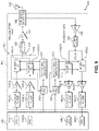
- FIG. 8 is a block diagram of an exemplary processor-based system that can include a semiconductor chip package in which inactive surfaces of a compound semiconductor die are treated with a passivation layer to diffuse encapsulation stress to surface micro-cracks caused by a molding compound as in the semiconductor chip packages in either of FIG. 2 or 5 ; and
- FIG. 9 is a block diagram of an exemplary wireless communications device that includes radio frequency (RP) components formed from a semiconductor chip package in which inactive surfaces of a III-V compound semiconductor die are treated to form a passivation layer to diffuse encapsulation stress to surface micro-cracks caused by a molding compound as in the semiconductor chip packages in either of FIG. 2 or 5 .
- RP radio frequency
- a III-V compound semiconductor die having a brittle crystalline structure includes an active region, including at least one functional circuit and an active surface, and an inactive region comprising a substrate comprising a back surface opposite to the active surface and a plurality of side surfaces.
- the plurality of side surfaces of the substrate are created with imperfections or micro-cracks during processes for shaping (e.g., dicing and/or thinning) the compound semiconductor die from a wafer.
- Micro-cracks can make the brittle crystalline structure of the III-V compound semiconductor die vulnerable to fracture under packaging-induced stresses.
- a semiconductor chip package includes a passivation layer on the plurality of side surfaces of the substrate to avoid fracture of the III-V compound semiconductor die.
- the semiconductor chip package includes the molding compound disposed on the passivation layer.
- the passivation layer avoids or prevents micro-cracks from propagating through the crystal structure of the III-V compound semiconductor die under the influence of the molding compound.
- the passivation layer is a passivated layer of the substrate of the compound semiconductor die.
- the passivation layer is a passivation material on the substrate.
- the passivated layer of the substrate is a native oxide of the III-V compound.
- the passivation material is a polycrystalline layer.
- processes for forming the passivation layer on the plurality of side surfaces to avoid packaging-induced fractures are disclosed.
- the processes for forming the passivation layer do not subject the III-V compound semiconductor die to high temperatures (>400° C.) that may degrade functional circuits.
- forming the passivation layer on the plurality of side surfaces of the substrate of the III-V compound semiconductor die includes treating the plurality of side surfaces to form the passivation layer.
- treating the plurality of side surfaces includes a treatment to form a passivated layer of the substrate on the plurality of side surfaces of the substrate.
- the treatment to form the passivated layer of the substrate includes an oxidation treatment forming a native oxide on the plurality of side surfaces by exposing the plurality of side surfaces to an oxygen plasma or using another oxidation method.
- the oxidation treatment removes the micro-cracks and transforms a surface layer of the substrate of the III-V compound semiconductor die into a thick native oxide that is less susceptible to fracture.
- treating the plurality of side surfaces includes depositing a passivation material, such as a polycrystalline layer, in and on the micro-cracks in the plurality of side surfaces to diffuse stresses induced by the molding compound. Treating the plurality of side surfaces of semiconductor dies to form passivation layers in flip-chip and wire-bond semiconductor chip packages as disclosed herein reduces incidence of failure caused by die fracturing.
- FIG. 1 is a magnified cross-sectional side view of a portion of a semiconductor chip package 100 that illustrates encapsulation stresses induced in micro-cracks on the surface of a semiconductor die.
- the semiconductor chip package 100 includes a III-V compound (e.g., gallium-arsenide (GaAs)) die 102 with an active surface 104 .
- the III-V compound die 102 is coupled in a flip-chip configuration to a substrate or laminate (not shown) by a solder bump 106 .
- Micro-cracks 108 are present along an inactive surface 110 of the III-V compound die 102 .
- a fracture 112 propagates from one of the micro-cracks 108 through the crystal lattice of the compound die 102 , causing the semiconductor chip package 100 to fail to operate.
- Each failure of a semiconductor chip package 100 reduces yield and increases manufacturing costs.
- FIG. 2 is a cross-sectional side view of a wire-bonded semiconductor chip package 200 (“chip package 200 ”) including a III-V compound semiconductor die 202 (“III-V compound die 202 ”) that includes a plurality of inactive surfaces 204 treated with a passivation layer 206 .
- the plurality of inactive surfaces 204 is a plurality of side surfaces 208 of the III-V compound die 202 .
- the passivation layer 206 is provided to avoid fracture of the III-V compound die 202 by reducing encapsulation stresses exerted on the plurality of inactive surfaces 204 by a molding compound 210 in contact with the passivation layer 206 on each of the plurality of inactive surfaces 204 .
- the molding compound 210 is employed to encapsulate the III-V compound die 202 in a structure of the chip package 200 and to isolate the III-V compound die 202 from its environment.
- the molding compound 210 may be in direct contact, meaning without anything intervening, or in indirect contact, meaning at least one intervening layer is between the molding compound 210 and the passivation layer 206 .
- the molding compound 210 exerts stress (i.e., force), referred to herein as encapsulation stress, on the passivation layer 206 .
- the encapsulation stress can arise from, for example, a difference in the rates of expansion or contraction of the III-V compound die 202 and the molding compound 210 in response to a change in temperature of the chip package 200 .
- Encapsulation stress may be a force parallel to or orthogonal to the inactive surfaces 204 .
- the III-V compound die 202 is formed from a wafer of a III-V compound 212 , which is any alloy of elements from Group III and Group V of the periodic table of elements, such as Gallium Arsenide (GaAs), for example.
- the III-V compound 212 may be an alloy of two or more elements.
- Transistors formed in III-V compound dies are capable of higher performance than transistors formed in silicon, but alloys of compounds are crystalline structures that are more brittle than silicon.
- the III-V compound die 202 includes a substrate 213 that is separated from the rest of the III-V compound wafer in a dicing process and further shaped (e.g., thinned) in additional processes.
- Dicing may be achieved by various methods including fully or partially cutting the wafer with a saw blade or a laser.
- the dicing process induces subsurface damage and micro-cracks on the substrate 213 , which can be particularly detrimental for packaging technologies that put a strain on the die.
- Imperfections, such as micro-cracks, formed along the side surfaces 208 of the substrate 213 of the compound die 202 due to the dicing process often provide potential sites for serious reliability problems, such as fracturing of the III-V compound die 202 . This is particularly true of III-V compound semiconductors, because of their brittleness.
- the molding compounds employed in the chip package 200 to encapsulate the III-V compound die 202 are generally composite materials such as epoxy mold compounds (EMCs) consisting of epoxy resins, curing agents, accelerators, fillers, flame retardants, adhesion promoters, phenolic hardeners, silicas, catalysts, pigments, and mold release agents.
- EMCs epoxy mold compounds
- the molding compound 210 may initially be in a viscous state, but solidifies to provide a structural exterior of the chip package 200 , and to protect the underlying III-V compound die 202 .
- the solidified molding compound 210 may have a different coefficient of thermal expansion than the III-V compound die 202 , which creates stresses at an intersection of the III-V compound die 202 and the molding compound 210 as a temperature of the chip package 200 changes. Having such stress exerted directly on a micro-crack could cause the micro-crack to propagate through the crystalline structure, causing the compound die 202 to fracture, but the passivation layer 206 formed on the inactive surfaces 204 avoids fracture of the III-V compound die 202 in one of two exemplary aspects.
- the passivation layer 206 on side surfaces 208 of the III-V compound die 202 in FIG. 2 is a passivated layer of the substrate 213 .
- the passivated layer is a native oxide of the compound 212 .
- the side surfaces 208 are treated by oxidizing the III-V compound 212 by exposing the side surfaces 208 to an oxygen plasma. Oxidation in this manner causes bonds of the crystalline structure of the compound 212 to be broken and the atoms to be rearranged as the oxygen molecules are absorbed into the surface.
- the surface layer of the III-V compound 212 is transformed into a thick native oxide, removing the micro-cracks from the crystalline structure.
- the native oxide is an arsenic oxide (e.g., As 2 O 3 ) or gallium oxide (Ga 2 O 3 ).
- an arsenic oxide e.g., As 2 O 3
- gallium oxide Ga 2 O 3
- a thick passivated layer i.e., native oxide
- the oxidation time depends on the setup, e.g., bias, frequency, and power employed in the application of the oxygen plasma, and may be in the range of minutes.
- the native oxide as the passivation layer 206 formed by this method is thicker than a naturally-occurring oxide formed in the presence of atmospheric oxygen.
- a naturally-occurring oxide may be in the range of up to about 30 angstroms, whereas a native oxide formed by exposure to an oxygen plasma may be at least 1 micron ( ⁇ m) and up to 2 ⁇ m in thickness, or thicker.
- a wet chemical process can be employed to treat the side surfaces 208 to form a native oxide.
- depositing the passivation material includes depositing a polycrystalline layer.
- the polycrystalline layer has a thickness of at least 0.1 ⁇ m.
- the passivation layer 206 including the polycrystalline layer fills and/or covers the micro-cracks and other imperfections. The polycrystalline layer spreads or diffuses external forces that, if applied directly to a micro-crack, could cause the micro-crack to propagate and fracture the III-V compound die 202 .
- the polycrystalline layer redirects these forces and avoids a fracture in the crystalline structure of the compound 212 .
- Silicon nitride (SiN) and silicon oxide (SiO) are examples of polycrystalline materials that can be deposited by tools such as plasma chemical vapor deposition (PCVD), for example, to form the passivation layer 206 .
- PCVD plasma chemical vapor deposition
- Other polycrystalline materials could also be deposited as a passivation layer.
- the III-V compound die 202 includes functional circuits 214 in an active region 215 including an active surface 216 .
- the active region 215 is adjacent to an inactive region 217 of the III-V compound die 202 .
- the inactive region 217 includes the substrate 213 .
- Functional circuits as disclosed herein are electrical and/or electronic circuits.
- the III-V compound die 202 is disposed on a layered substrate 218 that includes interconnects 220 to an external circuit (not shown).
- the active surface 216 of the III-V compound die 202 includes contacts 222 to the functional circuits 214 , and a back surface 224 of the III-V compound die 202 is bonded to the layered substrate 218 .
- the back surface 224 may be referred to herein as inactive because there are no functional circuits 214 on the back surface 224 .
- the chip package 200 also includes wire bonds 226 for electrically coupling the contacts 222 on the active surface 216 to the interconnects 220 on the layered substrate 218 .
- FIG. 3 is a flowchart illustrating a method 300 of fabricating the III-V compound die 202 employed in the chip package 200 in FIG. 2 .
- the method 300 is described below with reference to fabrication stages 400 A- 400 D illustrated in FIGS. 4 A- 4 D .
- FIG. 4 A is a cross-sectional side view of fabrication stage 400 A in which a semiconductor wafer 402 including the III-V compound 212 is bonded to a carrier 404 with the back surface 224 of the semiconductor wafer 402 facing the carrier 404 (block 302 ).
- the cross-sectional side views in FIGS. 4 A- 41 ) are views in a direction of a Z-axis of a plane including an X-axis and a Y-axis.
- the carrier 404 prevents damage to the surface of the semiconductor wafer 402 (e.g., by scratching) and/or breakage of the semiconductor wafer 402 (e.g., by deformation) as the carrier 404 is employed to physically manipulate the semiconductor wafer 402 through processing steps.
- the method 300 includes forming a plurality of functional circuits 214 in the active region 215 of the semiconductor wafer 402 in portions that will become the III-V compound dies 202 .
- the active region 215 includes an active surface ( 216 ) opposite to the back surface 224 of the semiconductor wafer 402 (block 304 ) which is coupled (e.g., bonded) to the carrier 404 .
- the method 300 further includes forming a protective layer 406 on the active surface 216 (block 306 ). The protective layer 406 protects the functional circuits 214 during subsequent processing.
- FIG. 4 B is a cross-sectional side view of fabrication stage 400 B which includes dicing the semiconductor wafer 402 into at least one III-V compound die 202 , each of the at least one III-V compound die 202 including the active region 215 and the inactive region 217 .
- the at least one III-V compound die 202 is diced from a portion of the semiconductor wafer 402 and may have a length dimension and a width dimension that are each in the range of about 1 millimeter (mm).
- a functional circuit 214 in the active region 215 of one III-V compound die 202 is one of the plurality of functional circuits 214 on the active region 215 of the semiconductor wafer 402 .
- the dicing exposes the side surfaces 208 of the substrate 213 of the one III-V compound die 202 .
- a back surface 224 of the substrate 213 of the one compound die 202 includes a portion of the semiconductor wafer 402 (block 308 ).
- the side surfaces 208 are exposed where portions of the semiconductor wafer 402 , dicing streets in the active surface 216 , are removed from between the portions of the semiconductor wafer 402 forming the at least one III-V compound die 202 .
- the carrier 404 is not cut in fabrication stage 400 B, and the at least one III-V compound die 202 remains bonded to the carrier 404 .
- FIG. 4 C is a cross-sectional side view of fabrication stage 400 C which includes forming the passivation layer 206 on the side surfaces 208 of the substrate 213 of the III-V compound die 202 (block 310 ).
- forming the passivation layer 206 can be achieved by treating the side surfaces 208 with an oxidation process to form a thick native oxide, or by depositing a polycrystalline layer, such as SiN or SiO, to the side surfaces 208 .
- the passivation layer 206 does not form on the protective layer 406 or on the carrier 404 .
- FIG. 4 D is a cross-sectional side view of fabrication stage 400 D which includes removing the protective layer 406 from the active surface 216 (block 312 ).
- Subsequent processes for forming the chip package 200 include removing the at least one III-V compound die 202 from the carrier 404 , and coupling one of the at least one III-V compound die 202 to a substrate (not shown). The processes further include electrically coupling the active surface 216 of the one III-V compound die 202 to the substrate with wire bonds.
- the chip package 200 is further formed by encapsulating the one III-V compound die 202 with the molding compound 210 .
- the passivation layer 206 is between the molding compound 210 and the side surfaces 208 of the one III-V compound die 202 .
- FIG. 5 is a cross-sectional side view of a flip-chip semiconductor chip package 500 (“chip package 500 ”) including a III-V compound semiconductor die 502 (“III-V compound die 502 ”) that includes one or more inactive surfaces 504 treated with a passivation layer 506 .
- the one or more inactive surfaces 504 are side surfaces 508 and a back surface 510 of a substrate 511 .
- the back surface 510 in FIG. 5 extends in an X-axis direction, and the side surfaces 508 extend in a Y-axis direction orthogonal to the X-axis direction.
- the III-V compound die 502 is coupled to a layered substrate 512 and is encapsulated by a molding compound 514 .
- the side surfaces 508 and the back surface 510 are all inactive surfaces, and each is treated with the passivation layer 506 configured to avoid fracture of the III-V compound die 502 by reducing encapsulation stress to the side surfaces 508 and the back surface 510 .
- the passivation layer 506 may be a passivated layer of the substrate 511 or a layer of passivation material deposited on the substrate 511 .
- the III-V compound die 502 is formed of a compound 516 , which is any alloy of elements from Group III and Group V of the periodic table of elements.
- a plurality of functional circuits 518 including logic circuits and/or memory circuits including transistors formed from the III-V compound 516 , are formed in an active region 519 including an active surface 520 of the compound die 502 .
- the active region 519 is adjacent to an inactive region 521 of the III-V compound die 502 .
- the inactive region 521 includes the substrate 511 .
- the active surface 520 extends in the X-axis direction on an opposite side of the III-V compound die 502 to the back surface 510 .
- the back surface 510 and the side surfaces 508 are inactive because they do not include functional circuits 518 .
- the active surface 520 of the compound die 502 faces the layered substrate 512 .
- a plurality of conductive bumps 522 between the active surface 520 and the layered substrate 512 , electrically couple the functional circuits 518 to interconnects 524 on the layered substrate 512 .
- the conductive bumps 522 may be, for example, solder bumps or solder balls formed of one or more conductive metals.
- the interconnects 524 are employed to mechanically and/or electrically couple the functional circuits 518 to an external circuit (not shown).
- each of the back surface 510 and the side surfaces 508 is treated with the passivation layer 506 to avoid fracturing of the III-V compound die 502 by reducing encapsulation stresses exerted by the molding compound 514 on the side surfaces 508 and the back surface 510 .
- the inactive surfaces 504 as described herein are not limited to a back surface 510 extending in the X-axis direction and one or more side surfaces 508 extending in the Y-axis direction, and could include surfaces not extending in either the X-axis direction or the Y-axis direction.
- FIG. 6 is a flowchart illustrating a method 600 of fabricating the III-V compound die 502 employed in the chip package 500 in FIG. 5 .
- the method 600 is described below with reference to fabrication stages 700 A- 700 G illustrated in FIGS. 7 A- 7 G .
- FIG. 7 A is a cross-sectional side view of fabrication stage 700 A in which a semiconductor wafer 702 including the III-V compound 516 is coupled to a first carrier 704 .
- the cross-sectional side views in FIGS. 7 A- 7 G are views in a direction of a Z-axis of a plane including an X-axis and a Y-axis.
- a purpose of the first carrier 704 is to allow the semiconductor wafer 702 to be physically manipulated during processing without damage.
- the method 600 includes forming the plurality of functional circuits 518 in the active region 519 of the semiconductor wafer 702 .
- the active region 519 includes the active surface 520 , which is opposite to a back side 706 of the semiconductor wafer 702 (block 602 ).
- the method 600 further includes forming a protective layer 708 on the active surface 520 and bonding the protective layer 708 to the first carrier 704 (block 604 ).
- the term “bonding” includes any applicable method of attaching as known
- FIG. 7 B is a cross-sectional side view of fabrication stage 700 B including thinning the back side 706 of the semiconductor wafer 702 to form the inactive back surface 510 (block 606 ).
- the semiconductor wafer 702 may be thinned from an initial wafer thickness of about 650 ⁇ m to a desired die thickness of about 200 ⁇ m of the III-V compound die 502 in the chip package 500 .
- the III-V compound die 502 in the flip-chip configuration in FIG. 5 is encapsulated by the molding compound 514 on the back surface 510 as well as the side surfaces 508 . Therefore, the back surface 510 is treated with the passivation layer 506 at separate steps from treating the side surfaces 508 with the passivation layer 506 in the method 600 , as explained herein.
- FIG. 7 C is a cross-sectional side view of fabrication stage 700 C including forming the passivation layer 506 configured to reduce encapsulation stress on the inactive back surface 510 of the semiconductor wafer 702 (block 608 ).
- the side surfaces 508 are not created until the semiconductor wafer 702 is diced, but dicing is performed with the active surface 520 exposed so a dicing tool can be visually aligned with dicing streets (not shown) on the active surface 520 .
- the dicing streets have a width of about 60 ⁇ m.
- the back surface 510 is first treated with the passivation layer 506 in the method 600 and, once the passivation layer 506 is provided, the semiconductor wafer 702 may be handled from the back side 706 for subsequent processing, such as dicing and treatment of the side surfaces 508 with the passivation layer 506 .
- FIG. 7 D is a cross-sectional side view of fabrication stage 700 D including bonding a second carrier 710 to the passivation layer 506 , and removing the first carrier 704 from the protective layer 708 (block 610 ). With the first carrier 704 removed from the protective layer 708 , the dicing tool can be aligned to the dicing streets on the active surface 520 . Fabrication stage 700 D in FIG. 7 D is similar to fabrication stage 400 A in FIG. 4 A . However, to protect the back surface 510 from being exposed to the molding compound 514 , the chip package 500 includes the passivation layer 506 between the semiconductor wafer 702 and the second carrier 710 .
- FIG. 7 E is a cross-sectional side view of fabrication stage 700 E including dicing the semiconductor wafer 702 into at least one III-V compound die 502 .
- Each of the at least one III-V compound die 502 includes the active region 519 and the inactive region 521 , which further includes the substrate 511 .
- the dicing exposes the side surfaces 508 of the III-V compound die 502 .
- the III-V compound die 502 from the semiconductor wafer 702 may have a length dimension and a width dimension that are each in the range of about 1 mm.
- a functional circuit 518 on the active surface 520 of one of the at least one compound die 502 includes one of the plurality of functional circuits 518 that are formed in the active region 519 of the semiconductor wafer 702 in FIGS.
- the side surfaces 508 of the substrate 511 are created and exposed where the semiconductor wafer 702 is separated or portions of the semiconductor wafer 702 are removed by the dicing tool from between the at least one III-V compound die 502 .
- a back surface 510 of the substrate 511 of the one III-V compound die 502 is formed from a portion of the back side 706 of the semiconductor wafer 702 (block 612 ).
- the second carrier 710 is not cut in the dicing process in fabrication stage 700 E, and the at least one compound die 502 remains coupled to the second carrier 710 .
- FIG. 7 F is a cross-sectional side view of fabrication stage 700 F which includes forming the passivation layer 506 on the side surfaces 508 of the substrate 511 of the at least one III-V compound die 502 (block 614 ).
- the passivation layer 506 extends continuously from the back surface 510 to the side surfaces 508 leaving none of the inactive surfaces of the at least one III-V compound die 502 exposed.
- forming the passivation layer 506 can include forming a passivation layer of the substrate 511 by treating the side surfaces 508 and on the back surface 510 with an oxidation process to form a thick native oxide.
- the passivation layer 506 can include depositing a passivation material on the side surfaces 508 and the back surface 510 by depositing a polycrystalline layer, such as SiN or SiO, for example, to the side surfaces 508 .
- the passivation layer 506 is not formed on the protective layer 708 or on the second carrier 710 .
- FIG. 7 G is a cross-sectional side view of fabrication stage 700 G which includes removing the protective layer 708 from the active surface 520 of the at least one compound die 502 (block 616 ).
- Subsequent processes for forming the chip package 500 include removing the at least one III-V compound die 502 from the second carrier 710 and coupling the at least one compound die 502 to the layered substrate 512 , with the active surface 520 of the at least one III-V compound die 502 facing the layered substrate 512 .
- the coupling comprises physically and/or electrically coupling the conductive bumps 522 to the functional circuits 518 and to the interconnects 524 of the layered substrate 512 .
- Forming the chip package 500 further includes encapsulating the at least one III-V compound die 502 with the molding compound 514 , with the passivation layer 506 between the molding compound 514 on the side surfaces 508 and the back surface 510 of the at least one III-V compound die 502 .
- Imperfections such as micro-cracks
- a semiconductor chip package in which inactive surfaces of a III-V compound die are treated with a passivation layer to prevent or avoid imperfections, such as micro-cracks, in the inactive surfaces from propagating to create a fracture in the III-V compound semiconductor die due to stresses exerted by a molding compound, as illustrated in any of FIGS. 2 and 5 , according to any aspects disclosed herein, may be provided in or integrated into any processor-based device.
- GPS
- FIG. 8 illustrates an example of a processor-based system 800 including a semiconductor chip package in which inactive surfaces of a III-V compound semiconductor die (“III-V compound die”) are treated with a passivation layer to prevent or avoid imperfections, such as micro-cracks, in the inactive surfaces from propagating to create a fracture in the III-V compound die due to stresses exerted by a molding compound, as illustrated in any of FIGS. 2 and 5 , and according to any aspects disclosed herein.
- the processor-based system 800 includes one or more central processor units (CPUs) 802 , which may also be referred to as CPU or processor cores, each including one or more processors 804 .
- CPUs central processor units
- the CPU(s) 802 may have cache memory 806 coupled to the processor(s) 804 for rapid access to temporarily stored data.
- the processor(s) 804 could include a semiconductor chip package in which inactive surfaces of a III-V compound die are treated with a passivation layer to prevent or avoid imperfections, such as micro-cracks, in the inactive surfaces from propagating to create a fracture in the III-V compound die due to stresses exerted by a molding compound, as illustrated in any of FIGS. 2 and 5 , and according to any aspects disclosed herein.
- the CPU(s) 802 is coupled to a system bus 808 and can intercouple master and slave devices included in the processor-based system 800 .
- the CPU(s) 802 communicates with these other devices by exchanging address, control, and data information over the system bus 808 .
- the CPU(s) 802 can communicate bus transaction requests to a memory controller 810 as an example of a slave device.
- a memory controller 810 as an example of a slave device.
- multiple system buses 808 could be provided, wherein each system bus 808 constitutes a different fabric.
- Other master and slave devices can be connected to the system bus 808 . As illustrated in FIG. 8 , these devices can include a memory system 812 that includes the memory controller 810 and one or more memory arrays 814 , one or more input devices 816 , one or more output devices 818 , one or more network interface devices 820 , and one or more display controllers 822 , as examples.
- Each of the memory system 812 , the one or more input devices 816 , the one or more output devices 818 , the one or more network interface devices 820 , and the one or more display controllers 822 can include a semiconductor chip package in which inactive surfaces of a III-V compound die are treated with a passivation layer to prevent or avoid imperfections, such as micro-cracks, in the inactive surfaces from propagating to create a fracture in the III-V compound die due to stresses exerted by a molding compound, as illustrated in any of FIGS. 2 and 5 , and according to any aspects disclosed herein.
- the input device(s) 816 can include any type of input device, including, but not limited to, input keys, switches, voice processors, etc.
- the output device(s) 818 can include any type of output device, including, but not limited to, audio, video, other visual indicators, etc.
- the network interface device(s) 820 can be any device configured to allow exchange of data to and from a network 824 .
- the network 824 can be any type of network, including, but not limited to, a wired or wireless network, a private or public network, a local area network (LAN), a wireless local area network (WLAN), a wide area network (WAN), a BLUETOOTHTM network, and the Internet.
- the network interface device(s) 820 can be configured to support any type of communications protocol desired.
- the CPU(s) 802 may also be configured to access the display controller(s) 822 over the system bus 808 to control information sent to one or more displays 826 .
- the display controller(s) 822 sends information to the display(s) 826 to be displayed via one or more video processors 828 , which process the information to be displayed into a format suitable for the display(s) 826 .
- the display(s) 826 can include any type of display, including, but not limited to, a cathode ray tube (CRT), a liquid crystal display (LCD), a plasma display, a light emitting diode (LED) display, etc.
- the display controller(s) 822 , display(s) 826 , and/or the video processor(s) 828 can include a semiconductor chip package in which inactive surfaces of a III-V compound die are treated with a passivation layer to prevent or avoid imperfections, such as micro-cracks, in the inactive surfaces from propagating to create a fracture in the III-V compound die due to stresses exerted by a molding compound, as illustrated in any of FIGS. 2 and 5 , and according to any aspects disclosed herein.
- FIG. 9 illustrates an exemplary wireless communications device 900 that includes radio frequency (RF) components formed from an integrated circuit (IC) 902 , wherein any of the components therein can include a semiconductor chip package in which inactive surfaces of a compound die are treated with a passivation layer to prevent or avoid imperfections, such as micro-cracks, in the inactive surfaces from propagating to create a fracture in the III-V compound die due to stresses exerted by a molding compound, as illustrated in any of FIGS. 2 and 5 , and according to any aspects disclosed herein.
- the wireless communications device 900 may include or be provided in any of the above-referenced devices, as examples. As shown in FIG. 9 , the wireless communications device 900 includes a transceiver 904 and a data processor 906 .
- the data processor 906 may include a memory to store data and program codes.
- the transceiver 904 includes a transmitter 908 and a receiver 910 that support bi-directional communications.
- the wireless communications device 900 may include any number of transmitters 908 and/or receivers 910 for any number of communication systems and frequency bands. All or a portion of the transceiver 904 may be implemented on one or more analog ICs, RF ICs (RFICs), mixed-signal ICs, etc.
- the transmitter 908 or the receiver 910 may be implemented with a super-heterodyne architecture or a direct-conversion architecture.
- a signal is frequency-converted between RF and baseband in multiple stages, e.g., from RF to an intermediate frequency (IF) in one stage, and then from IF to baseband in another stage for the receiver 910 .
- IF intermediate frequency
- the direct-conversion architecture a signal is frequency-converted between RF; and baseband in one stage.
- the super-heterodyne and direct-conversion architectures may use different circuit blocks and/or have different requirements.
- the transmitter 908 and the receiver 910 are implemented with the direct-conversion architecture.
- the data processor 906 processes data to be transmitted and provides I and Q analog output signals to the transmitter 908 .
- the data processor 906 includes digital-to-analog converters (DACs) 912 ( 1 ), 912 ( 2 ) for converting digital signals generated by the data processor 906 into the I and Q analog output signals, e.g., I and Q output currents, for further processing.
- DACs digital-to-analog converters
- lowpass filters 914 ( 1 ), 914 ( 2 ) filter the I and Q analog output signals, respectively, to remove undesired signals caused by the prior digital-to-analog conversion.
- Amplifiers (AMPs) 916 ( 1 ), 916 ( 2 ) amplify the signals from the lowpass filters 914 ( 1 ), 914 ( 2 ), respectively, and provide I and Q baseband signals.
- An upconverter 918 upconverts the I and Q baseband signals with I and Q transmit (TX) local oscillator (LO) signals through mixers 920 ( 1 ), 920 ( 2 ) from a TX LO signal generator 922 to provide an upconverted signal 924 .
- TX transmit
- LO local oscillator
- a filter 926 filters the upconverted signal 924 to remove undesired signals caused by the frequency upconversion as well as noise in a receive frequency band.
- a power amplifier (PA) 928 amplifies the upconverted signal 924 from the filter 926 to obtain the desired output power level and provides a transmitted RF signal.
- the transmitted RF signal is routed through a duplexer or switch 930 and transmitted via an antenna 932 .
- the antenna 932 receives signals transmitted by base stations and provides a received RF signal, which is routed through the duplexer or switch 930 and provided to a low noise amplifier (LNA) 934 .
- the duplexer or switch 930 is designed to operate with a specific receive (RX)-to-TX duplexer frequency separation, such that RX signals are isolated from TX signals.
- the received RF signal is amplified by the LNA 934 and filtered by a filter 936 to obtain a desired RF input signal.
- Downconversion mixers 938 ( 1 ), 938 ( 2 ) mix the output of the filter 936 with I and Q RX LO signals (i.e., LO_I and LO_Q) from an RX LO signal generator 940 to generate I and Q baseband signals.
- the I and Q baseband signals are amplified by AMPs 942 ( 1 ), 942 ( 2 ) and further filtered by lowpass filters 944 ( 1 ), 944 ( 2 ) to obtain and Q analog input signals, which are provided to the data processor 906 .
- the data processor 906 includes analog-to-digital converters (ADCs) 946 ( 1 ), 946 ( 2 ) for converting the analog input signals into digital signals to be further processed by the data processor 906 .
- ADCs analog-to-digital converters
- the TX LO signal generator 922 generates the I and Q TX LO signals used for frequency upconversion, while the RX LO signal generator 940 generates the I and Q RX LO signals used for frequency downconversion.
- Each LO signal is a periodic signal with a particular fundamental frequency.
- a TX phase-locked loop (PLL) circuit 948 receives timing information from the data processor 906 and generates a control signal used to adjust the frequency and/or phase of the TX LO signals from the TX LO signal generator 922 .
- an RX PLL circuit 950 receives timing information from the data processor 906 and generates a control signal used to adjust the frequency and/or phase of the RX LO signals from the RX LO signal generator 940 .
- DSP Digital Signal Processor
- ASIC Application Specific Integrated Circuit
- FPGA Field Programmable Gate Array
- a processor may be a microprocessor, but in the alternative, the processor may be any conventional processor, controller, microcontroller, or state machine.
- a processor may also be implemented as a combination of computing devices (e.g., a combination of a DSP and a microprocessor, a plurality of microprocessors, one or more microprocessors in conjunction with a DSP core, or any other such configuration).
- RAM Random Access Memory
- ROM Read Only Memory
- EPROM Electrically Programmable ROM
- EEPROM Electrically Erasable Programmable ROM
- registers a hard disk, a removable disk, a CD-ROM, or any other form of computer readable medium known in the art.
- An exemplary storage medium is coupled to the processor such that the processor can read information from, and write information to, the storage medium.
- the storage medium may be integral to the processor.
- the processor and the storage medium may reside in an ASIC.
- the ASIC may reside in a remote station.
- the processor and the storage medium may reside as discrete components in a remote station, base station, or server.
Landscapes
- Engineering & Computer Science (AREA)
- Microelectronics & Electronic Packaging (AREA)
- Computer Hardware Design (AREA)
- Power Engineering (AREA)
- General Physics & Mathematics (AREA)
- Physics & Mathematics (AREA)
- Condensed Matter Physics & Semiconductors (AREA)
- Manufacturing & Machinery (AREA)
- Chemical & Material Sciences (AREA)
- Ceramic Engineering (AREA)
- Dicing (AREA)
- Formation Of Insulating Films (AREA)
- Structures Or Materials For Encapsulating Or Coating Semiconductor Devices Or Solid State Devices (AREA)
Abstract
Description
Claims (13)
Priority Applications (7)
| Application Number | Priority Date | Filing Date | Title |
|---|---|---|---|
| US16/868,147 US11545404B2 (en) | 2020-05-06 | 2020-05-06 | III-V compound semiconductor dies with stress-treated inactive surfaces to avoid packaging-induced fractures, and related methods |
| TW110114556A TW202209510A (en) | 2020-05-06 | 2021-04-22 | Iii-v compound semiconductor dies with stress-treated inactive surfaces to avoid packaging-induced fractures, and related methods |
| PCT/US2021/029200 WO2021225818A1 (en) | 2020-05-06 | 2021-04-26 | Iii-v compound semiconductor dies with stress-treated inactive surfaces and manufacturing methods thereof |
| BR112022021544A BR112022021544A2 (en) | 2020-05-06 | 2021-04-26 | III-V SEMICONDUCTOR COMPOUND MATRIX WITH VOLTAGE-TREATED INACTIVE SURFACES AND MANUFACTURING METHODS THEREOF |
| EP21726483.7A EP4147271A1 (en) | 2020-05-06 | 2021-04-26 | Iii-v compound semiconductor dies with stress-treated inactive surfaces and manufacturing methods thereof |
| KR1020227037520A KR20230006817A (en) | 2020-05-06 | 2021-04-26 | III-V Compound Semiconductor Dies with Stress Treated Inactive Surfaces, and Manufacturing Methods Thereof |
| CN202180030646.2A CN115485825A (en) | 2020-05-06 | 2021-04-26 | III-V compound semiconductor die with stressed passive surface and method of making same |
Applications Claiming Priority (1)
| Application Number | Priority Date | Filing Date | Title |
|---|---|---|---|
| US16/868,147 US11545404B2 (en) | 2020-05-06 | 2020-05-06 | III-V compound semiconductor dies with stress-treated inactive surfaces to avoid packaging-induced fractures, and related methods |
Publications (2)
| Publication Number | Publication Date |
|---|---|
| US20210351095A1 US20210351095A1 (en) | 2021-11-11 |
| US11545404B2 true US11545404B2 (en) | 2023-01-03 |
Family
ID=75977808
Family Applications (1)
| Application Number | Title | Priority Date | Filing Date |
|---|---|---|---|
| US16/868,147 Active US11545404B2 (en) | 2020-05-06 | 2020-05-06 | III-V compound semiconductor dies with stress-treated inactive surfaces to avoid packaging-induced fractures, and related methods |
Country Status (7)
| Country | Link |
|---|---|
| US (1) | US11545404B2 (en) |
| EP (1) | EP4147271A1 (en) |
| KR (1) | KR20230006817A (en) |
| CN (1) | CN115485825A (en) |
| BR (1) | BR112022021544A2 (en) |
| TW (1) | TW202209510A (en) |
| WO (1) | WO2021225818A1 (en) |
Families Citing this family (1)
| Publication number | Priority date | Publication date | Assignee | Title |
|---|---|---|---|---|
| TWI817552B (en) * | 2022-06-13 | 2023-10-01 | 欣興電子股份有限公司 | Package structure and manufacturing method thereof |
Citations (13)
| Publication number | Priority date | Publication date | Assignee | Title |
|---|---|---|---|---|
| US20030137062A1 (en) * | 1996-09-20 | 2003-07-24 | Salman Akram | Use of nitrides for flip-chip encapsulation |
| US20080290511A1 (en) * | 2005-11-11 | 2008-11-27 | Koninklijke Philips Electronics, N.V. | Chip Assembly and Method of Manufacturing Thereof |
| US20100213485A1 (en) * | 2007-07-19 | 2010-08-26 | Photonstar Led Limited | Vertical led with conductive vias |
| US8759865B2 (en) * | 2010-08-03 | 2014-06-24 | Industrial Technology Research Institute | Light emitting diode chip, light emitting diode package structure, and method for forming the same |
| US20160254188A1 (en) | 2015-02-27 | 2016-09-01 | Disco Corporation | Wafer dividing method |
| US20170011982A1 (en) * | 2015-07-06 | 2017-01-12 | Infineon Technologies Ag | Insulated die |
| US20170263526A1 (en) | 2016-03-11 | 2017-09-14 | Panasonic Intellectual Property Management Co., Ltd. | Element chip and method for manufacturing the same |
| US20170287782A1 (en) * | 2016-03-30 | 2017-10-05 | International Business Machines Corporation | Ir assisted fan-out wafer level packaging using silicon handler |
| US9978644B1 (en) | 2016-09-07 | 2018-05-22 | Amkor Technology, Inc. | Semiconductor device and manufacturing method |
| US10006822B2 (en) * | 2016-06-21 | 2018-06-26 | Melexis Technologies Nv | Semiconductor sensor assembly for harsh media application |
| US10090812B2 (en) * | 2012-06-14 | 2018-10-02 | Skyworks Solutions, Inc. | Power amplifier modules with bonding pads and related systems, devices, and methods |
| US20200219815A1 (en) * | 2017-12-29 | 2020-07-09 | Intel Corporation | Microelectronic assemblies with communication networks |
| US20210111147A1 (en) * | 2017-12-29 | 2021-04-15 | Intel Corporation | Microelectronic assemblies |
-
2020
- 2020-05-06 US US16/868,147 patent/US11545404B2/en active Active
-
2021
- 2021-04-22 TW TW110114556A patent/TW202209510A/en unknown
- 2021-04-26 WO PCT/US2021/029200 patent/WO2021225818A1/en unknown
- 2021-04-26 BR BR112022021544A patent/BR112022021544A2/en unknown
- 2021-04-26 EP EP21726483.7A patent/EP4147271A1/en active Pending
- 2021-04-26 CN CN202180030646.2A patent/CN115485825A/en active Pending
- 2021-04-26 KR KR1020227037520A patent/KR20230006817A/en active Search and Examination
Patent Citations (13)
| Publication number | Priority date | Publication date | Assignee | Title |
|---|---|---|---|---|
| US20030137062A1 (en) * | 1996-09-20 | 2003-07-24 | Salman Akram | Use of nitrides for flip-chip encapsulation |
| US20080290511A1 (en) * | 2005-11-11 | 2008-11-27 | Koninklijke Philips Electronics, N.V. | Chip Assembly and Method of Manufacturing Thereof |
| US20100213485A1 (en) * | 2007-07-19 | 2010-08-26 | Photonstar Led Limited | Vertical led with conductive vias |
| US8759865B2 (en) * | 2010-08-03 | 2014-06-24 | Industrial Technology Research Institute | Light emitting diode chip, light emitting diode package structure, and method for forming the same |
| US10090812B2 (en) * | 2012-06-14 | 2018-10-02 | Skyworks Solutions, Inc. | Power amplifier modules with bonding pads and related systems, devices, and methods |
| US20160254188A1 (en) | 2015-02-27 | 2016-09-01 | Disco Corporation | Wafer dividing method |
| US20170011982A1 (en) * | 2015-07-06 | 2017-01-12 | Infineon Technologies Ag | Insulated die |
| US20170263526A1 (en) | 2016-03-11 | 2017-09-14 | Panasonic Intellectual Property Management Co., Ltd. | Element chip and method for manufacturing the same |
| US20170287782A1 (en) * | 2016-03-30 | 2017-10-05 | International Business Machines Corporation | Ir assisted fan-out wafer level packaging using silicon handler |
| US10006822B2 (en) * | 2016-06-21 | 2018-06-26 | Melexis Technologies Nv | Semiconductor sensor assembly for harsh media application |
| US9978644B1 (en) | 2016-09-07 | 2018-05-22 | Amkor Technology, Inc. | Semiconductor device and manufacturing method |
| US20200219815A1 (en) * | 2017-12-29 | 2020-07-09 | Intel Corporation | Microelectronic assemblies with communication networks |
| US20210111147A1 (en) * | 2017-12-29 | 2021-04-15 | Intel Corporation | Microelectronic assemblies |
Non-Patent Citations (10)
| Title |
|---|
| BURTE E. P., SCHULZE G. H.: "THE CORRELATION BETWEEN THE BREAKDOWN VOLTAGE OF POWER DEVICES PASSIVATED BY SEMI-INSULATING POLYCRYSTALLINE SILICON AND THE EFFECTIVE DENSITY OF INTERFACE CHARGES.", IEEE TRANSACTIONS ON ELECTRON DEVICES, IEEE, USA, vol. 38., no. 06., 1 June 1991 (1991-06-01), USA, pages 1505 - 1509., XP000205849, ISSN: 0018-9383, DOI: 10.1109/16.81646 |
| Burte, E.P., et al., "The Correlation Between the Breakdown Voltage of Power Devices Passivated by Semi-Insulating Polycrystalline Silicon and The Effective Density of Interface Charges", IEEE Transactions on Electron Devices, IEEE Service Center, Pisacataway, NJ, vol. 38, No. 6, Jun. 1, 1991 (Jun. 1, 1991), XP000205849, pp. 1505-1509, ISSN: 0018-9383, DOI: 10.1109/16.81646 the whole document. |
| International Search Report and Written Opinion for International Patent Application No. PCT/US2021/029200, dated Aug. 9, 2021, 18 pages. |
| Raj, G. et al., "Polarization and Breakdown Analysis of AlGaN Channel HEMTs with AIN Buffer," World Journal of Condensed Matter Physics, vol. 5, 2015, Scientific Research Publishing, pp. 232-243. |
| WANG, C.-C. HUANG, H.-K. WANG, Y.-H. HOUNG, M.-P. WU, C.-L. CHANG, C.-S.: "Fabrication of GaAs Schottky diode by liquid phase chemical enhanced oxidation", SOLID STATE ELECTRONICS., ELSEVIER SCIENCE PUBLISHERS, BARKING., GB, vol. 48, no. 9, 1 September 2004 (2004-09-01), GB , pages 1683 - 1686, XP004518824, ISSN: 0038-1101, DOI: 10.1016/j.sse.2004.03.003 |
| Wang, C-C., et al., "Fabrication of GaAs Schottky Diode by Liquid Phase Chemical Enhanced Oxidation", Solid State Electronics, Elsevier Science Publishers, Barking, GB, vol. 48, No. 9, Sep. 1, 2004 (Sep. 1, 2004), XP004518824, pp. 1683-1686, ISSN: 0038-1101, DOI:10.1016/J.SSE.2004.03.003 2. Experimental. |
| Watanabe, K. et al., "Quantitative In-depth Profile of Passivated Oxide Layers of GaAs by AES-SIMS—a Comparison of Thermal, Anodic and Plasma Oxidations," Proceedings of the 9th Conference on Solid State Devices, Tokyo, 1977; Japanese Journal of Applied Physics, vol. 17, Supplement 17-1, 1978, pp. 335-340. |
| WILMSEN C: "Physics and Chemistry of Iii-V Compound Semiconductor Interfaces", vol. chapter 7, 1 January 1985, KLUWER ACADEMIC PUBLISHERS , US , ISBN: 978-0-306-41769-6, article WILMSEN C W: "Oxide/III-V compound semiconductor interfaces", pages: 403 - 462, XP008098095 |
| Wilmsen, C.W., "Oxide/III-V Compound Semiconductor Interfaces", Jan. 1, 1985 (Jan. 1, 1985), Physics and Chemistry of III-V Compound Semiconductor Interfaces, Kluwer Academic Publishers, US, XP008098095, pp. 403-462, ISBN: 978-0-306-41769-6, 5. Plasma-Grown Oxide, pp. 453-456, figure 28. |
| Yamasaki, K. et al., "Anodic Oxidation of GaAs Using Oxygen Plasma," Proceedings of the 9th Conference on Solid State Devices, Tokyo, 1977; Japanese Journal of Applied Physics, vol. 17, Supplement 17-1, 1978, pp. 321-336. |
Also Published As
| Publication number | Publication date |
|---|---|
| BR112022021544A2 (en) | 2022-12-20 |
| US20210351095A1 (en) | 2021-11-11 |
| TW202209510A (en) | 2022-03-01 |
| KR20230006817A (en) | 2023-01-11 |
| CN115485825A (en) | 2022-12-16 |
| EP4147271A1 (en) | 2023-03-15 |
| WO2021225818A1 (en) | 2021-11-11 |
Similar Documents
| Publication | Publication Date | Title |
|---|---|---|
| US7626251B2 (en) | Microelectronic die assembly having thermally conductive element at a backside thereof and method of making same | |
| US10483248B2 (en) | Wafer level chip scale filter packaging using semiconductor wafers with through wafer vias | |
| US20210280523A1 (en) | Integrated circuit (ic) packages employing split, double-sided metallization structures to facilitate a semiconductor die ("die") module employing stacked dice, and related fabrication methods | |
| US11545404B2 (en) | III-V compound semiconductor dies with stress-treated inactive surfaces to avoid packaging-induced fractures, and related methods | |
| US20080009095A1 (en) | Advanced Thin Flexible Microelectronic Assemblies and Methods for Making Same | |
| TW202306094A (en) | Split die integrated circuit (ic) packages employing die-to-die (d2d) connections in die-substrate standoff cavity, and related fabrication methods | |
| US20210242160A1 (en) | Integrated circuit (ic) packages employing a thermal conductive package substrate with die region split, and related fabrication methods | |
| US20080029865A1 (en) | Electronic Device and Method For Producing the Same | |
| US11456291B2 (en) | Integrated circuit (IC) packages employing split, double-sided metallization structures to facilitate a semiconductor die (“die”) module employing stacked dice, and related fabrication methods | |
| US20220199547A1 (en) | FAN-OUT WAFER-LEVEL PACKAGING (FOWLP) INTEGRATED CIRCUITS (ICs) EMPLOYING AN ELECTRO-MAGNETIC INTERFERENCE (EMI) SHIELD STRUCTURE IN UNUSED FAN-OUT AREA FOR EMI SHIELDING, AND RELATED FABRICATION METHODS | |
| US11742253B2 (en) | Selective mold placement on integrated circuit (IC) packages and methods of fabricating | |
| WO2022064678A1 (en) | Semiconductor device, and manufacturing method therefor | |
| US20220068780A1 (en) | Integrated circuit (ic) package substrate with embedded trace substrate (ets) layer on a substrate, and related fabrication methods | |
| US20230090842A1 (en) | Multi-level stacked acoustic wave (aw) filter packages and related fabrication methods | |
| US20230299048A1 (en) | Three-dimensional (3d) integrated circuit (ic) (3dic) package with a bottom die layer employing an extended interposer substrate, and related fabrication methods | |
| US20220069453A1 (en) | Device, package and/or substrate comprising curved antenna | |
| US20230207486A1 (en) | Interlayer dielectric stack optimization for wafer bow reduction | |
| KR20230066567A (en) | Integrated Circuit (IC) with Reconfigured Die Interposer for Improved Connectivity, and Related Manufacturing Methods | |
| KR20220163370A (en) | Systems and methods for packaging an acoustic device included in an integrated circuit (IC) | |
| WO2023164323A1 (en) | Antenna modules employing three-dimensional (3d) build-up on mold package to support efficient integration of radio-frequency (rf) circuitry, and related fabrication methods | |
| KR20210133898A (en) | Semiconductor package and manufacturing method thereof |
Legal Events
| Date | Code | Title | Description |
|---|---|---|---|
| AS | Assignment |
Owner name: QUALCOMM INCORPORATED, CALIFORNIA Free format text: ASSIGNMENT OF ASSIGNORS INTEREST;ASSIGNORS:TAO, GENGMING;YANG, BIN;LI, XIA;REEL/FRAME:052590/0186 Effective date: 20200130 |
|
| FEPP | Fee payment procedure |
Free format text: ENTITY STATUS SET TO UNDISCOUNTED (ORIGINAL EVENT CODE: BIG.); ENTITY STATUS OF PATENT OWNER: LARGE ENTITY |
|
| STPP | Information on status: patent application and granting procedure in general |
Free format text: RESPONSE TO NON-FINAL OFFICE ACTION ENTERED AND FORWARDED TO EXAMINER |
|
| STPP | Information on status: patent application and granting procedure in general |
Free format text: NON FINAL ACTION MAILED |
|
| STPP | Information on status: patent application and granting procedure in general |
Free format text: RESPONSE TO NON-FINAL OFFICE ACTION ENTERED AND FORWARDED TO EXAMINER |
|
| STPP | Information on status: patent application and granting procedure in general |
Free format text: FINAL REJECTION MAILED |
|
| STPP | Information on status: patent application and granting procedure in general |
Free format text: RESPONSE AFTER FINAL ACTION FORWARDED TO EXAMINER |
|
| STPP | Information on status: patent application and granting procedure in general |
Free format text: NOTICE OF ALLOWANCE MAILED -- APPLICATION RECEIVED IN OFFICE OF PUBLICATIONS |
|
| STPP | Information on status: patent application and granting procedure in general |
Free format text: PUBLICATIONS -- ISSUE FEE PAYMENT RECEIVED |
|
| STCF | Information on status: patent grant |
Free format text: PATENTED CASE |