US11438076B2 - Optical quantum networks with rare-earth ions - Google Patents
Optical quantum networks with rare-earth ions Download PDFInfo
- Publication number
- US11438076B2 US11438076B2 US16/937,379 US202016937379A US11438076B2 US 11438076 B2 US11438076 B2 US 11438076B2 US 202016937379 A US202016937379 A US 202016937379A US 11438076 B2 US11438076 B2 US 11438076B2
- Authority
- US
- United States
- Prior art keywords
- qubit
- microwave
- optical
- state
- rare
- Prior art date
- Legal status (The legal status is an assumption and is not a legal conclusion. Google has not performed a legal analysis and makes no representation as to the accuracy of the status listed.)
- Active, expires
Links
Images


Classifications
-
- H—ELECTRICITY
- H04—ELECTRIC COMMUNICATION TECHNIQUE
- H04B—TRANSMISSION
- H04B10/00—Transmission systems employing electromagnetic waves other than radio-waves, e.g. infrared, visible or ultraviolet light, or employing corpuscular radiation, e.g. quantum communication
- H04B10/70—Photonic quantum communication
-
- G—PHYSICS
- G06—COMPUTING; CALCULATING OR COUNTING
- G06N—COMPUTING ARRANGEMENTS BASED ON SPECIFIC COMPUTATIONAL MODELS
- G06N10/00—Quantum computing, i.e. information processing based on quantum-mechanical phenomena
-
- B—PERFORMING OPERATIONS; TRANSPORTING
- B82—NANOTECHNOLOGY
- B82Y—SPECIFIC USES OR APPLICATIONS OF NANOSTRUCTURES; MEASUREMENT OR ANALYSIS OF NANOSTRUCTURES; MANUFACTURE OR TREATMENT OF NANOSTRUCTURES
- B82Y10/00—Nanotechnology for information processing, storage or transmission, e.g. quantum computing or single electron logic
-
- B—PERFORMING OPERATIONS; TRANSPORTING
- B82—NANOTECHNOLOGY
- B82Y—SPECIFIC USES OR APPLICATIONS OF NANOSTRUCTURES; MEASUREMENT OR ANALYSIS OF NANOSTRUCTURES; MANUFACTURE OR TREATMENT OF NANOSTRUCTURES
- B82Y20/00—Nanooptics, e.g. quantum optics or photonic crystals
Definitions
- qubits may be provided by single ytterbium 171 ( 171 Yb 3+ ) ions that are doped into a crystal structure, such as yttrium orthovanadate (YVO) crystal structure ( 171 Yb 3+ :YVO).
- YVO yttrium orthovanadate
- Quantum networks as exemplified in FIG. 5 , in which quantum nodes for processing and storing quantum information are connected by quantum channels (like optical fibers), have emerged as a route to building scalable and flexible quantum-enhanced technologies that can make use of relatively elementary quantum systems currently available.
- Optical photons are excellent carriers of quantum information and the ideal candidate for establishing long-distance, room-temperature links between quantum nodes.
- the challenge lies in finding a way to map information efficiently and reversibly from light (photons) into quantum nodes where it can be stored and processed.
- the development of such quantum light-matter interfaces is then of vital importance to the successful implementation of a quantum network.
- solid-state spins with optical transitions offer a promising route to robust and scalable light-matter interfaces.
- optically-addressable solid-state spins currently being investigated for this application including quantum dots, color centers in diamond or silicon carbide, donors in silicon, and rare-earth ions in solids.
- a solid-state quantum emitter In order for a solid-state quantum emitter to be useful in the context of a quantum network, it must have long spin coherence (millisecond or longer) lifetimes to enable storage of quantum information and spectrally stable optical transitions to enable the generation of indistinguishable photons necessary for entanglement generation. To enable the efficient extraction of emitted photons into a well-defined optical mode, these emitters should be coupled to optical cavities or resonators. Crucially, the emitters must maintain their desired spin and optical properties when integrated into these cavities. Finding a system that can satisfy these requirements is a fundamental challenge in the field of solid-state quantum emitters. Teachings according to the present disclosure address such challenge.
- REIs Rare-earth ions doped into crystalline hosts have demonstrated significant progress in implementing solid-state quantum technologies.
- REIs possess some of the longest optical lifetimes (millisecond) and spin coherence lifetimes (hours) in the solid state, which has provided the foundation for numerous demonstrations of quantum memories and quantum interfaces.
- REIs with an odd number of electrons i.e. Kramers ions
- the large magnetic moments of these ions allow for strong interactions with microwaves, enabling fast operations and the potential for interfacing with superconducting qubits.
- Isotopes of these ions with non-zero nuclear spin also offer the possibility of long-term quantum storage. This combination of properties creates the potential for building interfaces between microwave photons, optical photons, and long-lived nuclear spins.
- ytterbium is an attractive choice due to its simple level structure consisting of only two electronic multiplets (respectively labelled in FIG. 1A as 2 F 7/2 having lower energy levels used as ground state, and 2 F 5/2 having higher energy levels used as excited state).
- the optical transition between the lowest energy levels of these multiplets occurs around 980 nm (e.g., FIG. 1A later described), which is readily accessible by laser sources such as standard diode lasers.
- the 171 Yb 3+ isotope is unique among the trivalent REIs as the only Kramers ion with a nuclear spin of 1 ⁇ 2.
- Yttrium orthovanadate YVO 4 , or YVO
- YVO yttrium orthovanadate
- a rare-earth based quantum bit comprising: a doped crystal ( 171 Yb 3+ :YVO) comprising a ytterbium 171 ( 171 Yb 3+ ) ion doped into a yttrium orthovanadate (YVO) host crystal; a nanophotonic cavity coupled to the doped crystal; first and second laser sources coupled to the 171 Yb 3+ ion through the nanophotonic cavity; and first and second microwave sources coupled to the 171 Yb 3+ ion through a microwave waveguide, wherein: a zero-field energy level structure of the rare-earth qubit provided by the 171 Yb 3+ ion comprises: optical transitions between lower energy level ground states and higher energy level excited states, the optical transitions addressable via optical pulses generated by the first and second laser sources, and first and second microwave transitions within respective ground states and excited states, the first microwave transition addressable via microwave pulse
- a rare-earth based quantum bit comprising: a doped crystal comprising a ytterbium 171 ( 171 Yb 3+ ) ion doped into a host crystal; a nanophotonic cavity fabricated in the doped crystal; wherein: a zero-field energy level structure of the rare-earth qubit provided by the 171 Yb 3+ ion comprises: optical transitions between lower energy level ground states and higher energy level excited states, the optical transitions addressable via optical pulses, and first and second microwave transitions within respective ground states and excited states, the first microwave and second microwave transitions addressable via microwave pulses.
- a method for realizing a rare-earth based quantum bit comprising: doping a ytterbium 171 ( 171 Yb 3+ ) ion into a yttrium orthovanadate (YVO) host crystal, thereby obtaining a doped crystal (171Yb 3+ :YVO); fabricating a nanophotonic cavity in the doped crystal; based on the doping, obtaining a zero-field energy level structure of the rare-earth qubit provided by the 171 Yb 3+ ion, said structure comprising: i) optical transitions A, E and F between lower energy level ground states and higher energy level excited states at a wavelength that is longer than 980 nm; and ii) microwave transitions f g and f e within respective ground states and excited states; addressing the optical transitions via optical pulses generated by first and second laser sources coupled to the 171Yb3+ ion through the nano
- FIG. 1A shows a zero-field energy level structure of a qubit provided by a 171 Yb 3+ ion doped into a yttrium orthovanadate (YVO) crystal structure ( 171 Yb 3+ :YVO).
- YVO yttrium orthovanadate
- FIG. 1B shows an exemplary sequence according to the present disclosure used to initialize the qubit of FIG. 1A into a state
- FIG. 1C shows a block diagram according to an exemplary embodiment of the present disclosure used to operate the qubit according to the sequence of FIG. 1B .
- FIG. 1D shows a line drawing based on a scanning electron microscope (SEM) image of a photonic crystal cavity fabricated in a YVO crystal structure doped by single 171 Yb 3+ ions.
- SEM scanning electron microscope
- FIG. 1E shows a single 171 Yb 3+ ion doped into a yttrium orthovanadate (YVO) crystal structure ( 171 Yb 3+ :YVO).
- YVO yttrium orthovanadate
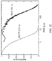
- FIG. 2A shows a graph representative of a photoluminescence excitation (PLE) spectrum showing resolved peaks corresponding to single 171 Yb 3+ ions doped in the (YVO) crystal structure ( 171 Yb 3+ :YVO).
- PLE photoluminescence excitation
- FIG. 2B shows a graph representative of a pulsed autocorrelation measurement on the ion X shown in FIG. 2A .
- FIG. 2C shows a graph representative of a normalised photoluminescence emission from the ion X of FIG. 2A compared to typical photoluminescence from ions in bulk crystal.
- FIG. 3A shows graphs representative of the probability of finding the 171 Yb 3+ ion in either spin state
- FIG. 3B shows graphs representative of the probability of finding the 171 Yb 3+ ion in either spin state
- FIG. 4A shows a single-shot readout (SSRO) sequence according to an embodiment of the present disclosure of a single 171 Yb 3+ ion doped into a yttrium orthovanadate (YVO) crystal structure ( 171 Yb 3+ :YVO).
- SSRO single-shot readout
- FIG. 4B shows graphs representative of photon-count distributions for first and second read sequences used in the SSRO of FIG. 4A for the 171 Yb 3+ ion initially prepared in the spin state
- FIG. 4C shows graphs representative of probability distribution of assigned states (i, j) for the first and second read sequences used in the SSRO of FIG. 4A for the 171 Yb 3+ ion initially prepared in the spin state
- FIG. 5 shows a schematic of an exemplary optical quantum network for entangling a first node to a last node.
- spin-spin entanglement between distant rare-earth ions may first require spin-photon entanglement between a single REI and an optical photon.
- spin-photon entanglement may require the ability to excite and collect the emission from a single ion (i.e., REI) without collecting photons from other ions that are part of a crystal structure (e.g., YVO) within which the REI is entrapped.
- a central challenge with building REI-based quantum interfaces is that their exceptional coherence properties come at the expense of weak optical transitions.
- the slow optical photon emission and collection rate from a single rare-earth ion in a bulk crystal makes it difficult to optically identify and isolate a corresponding signature from the background emission rate with high signal-to-noise ratio.
- most REI-based interfaces to date have relied on the collective absorption of large ensembles of REIs to achieve efficient interaction with light and thereby allowing detection of a corresponding (collective) signature.
- teachings according to the present disclosure overcome the above challenges with REI-based interfaces by coupling ytterbium ( 171 Yb 3+ ) ions to a nanophotonic cavity (i.e., nanophotonic resonator). This allows overcoming the relatively weak optical transitions of the REIs ( 171 Yb 3+ ) and enable detection and coherent manipulation of a single ytterbium ion which can therefore be used, for example, as a single optical photon emitter in a node of a quantum network as shown in FIG. 5 (later described).
- the 171 Yb 3+ ions are coupled to a photonic (crystal) cavity by fabricating such cavity in an, e.g., YVO host crystal that is doped with the 171 Yb 3+ ions.
- the 171 Yb 3+ ions concentration relative to the host crystal is around 20 parts per billion with respect to yttrium (e.g., Y of the host crystal shown in FIG. 1E ).
- such cavity can be fabricated to provide a relatively small optical mode volume (e.g., about ⁇ 1( ⁇ /n YVO ) 3 ) and a large quality factor (e.g., 1 ⁇ 10 4 or higher), thereby increasing the cavity quality factor to mode volume ratio.
- This in turn enhances the emission rate, collection efficiency, and cyclicity of optical transitions (e.g., transition A and E described with reference to FIG. 1A ) emitted by the REI via, for example, the known in the art Purcell effect.
- FIG. 1A shows a zero-field energy level structure of a qubit provided by a 171Yb 3+ ion coupled to the photonic cavity according to the present disclosure.
- Optical transitions A and E are coupled (co-polarized) to the cavity mode, while the transition F is cross-polarized to the cavity mode.
- the relatively large hyperfine interaction by the level structure shown in FIG. 1A means that the three optical transitions (A, E, F) can be easily resolved in an optical transmission spectrum through the cavity at zero magnetic field. As can be seen in FIG.
- the optical transitions (emissions) A, E and F are associated with transitions between various spin states labelled as
- g stands for ground and “e” for excited.
- FIG. 1A other transitions (not labelled in FIG. 1A ) between the various labelled states do exist, some such transitions being possible only with a non-zero magnetic field.
- addressing of the three transitions (A, E, F) of the zero-field energy level structure shown in FIG. 1A and obtaining excitation results according to the present teachings is only possible at zero magnetic field. In other words, care is taken to eliminate any coupling of magnetic fields to the 171 Yb 3+ ion, including any stray magnetic field, such as to obtain a true “zero-field”.
- spin states are denoted according to the form:
- 171 Yb 3+ the only paramagnetic rare-earth isotope with a nuclear spin of 1 ⁇ 2, provides a favourable combination of the simple hyperfine structure shown in FIG. 1A , which can be used as a qubit and clock transitions with long coherence times.
- 171 Yb 3+ directly substitutes for Y 3+ in a site that has non-polar symmetry (D 2d ), which results in no first-order DC stark effect and thus reduces the sensitivity to electric field fluctuations that can cause optical decoherence.
- 1 g spin states have zero net magnetic moment and as a result the
- 1 g transition retains the strength of an electron spin transition, which enables fast and efficient microwave manipulation.
- Teachings according to the present disclosure use states
- the shown zero-field energy level structure of the qubit according to the present disclosure can be provided at temperatures greater than 1K (Kelvin).
- 1K Kelvin
- a person skilled in the art will appreciate practical aspect of operation according to such relatively high (hot) temperature which can be achieved using relatively common cryostats based on helium 4 that is an abundant resource.
- Lower (colder) temperatures generally require helium 3 that is produced in nuclear reactors and is orders of magnitude more expensive than helium 4.
- the cavity-enhanced optical transitions provided by the coupled 171 Yb 3+ ions enable coherent optical control and efficient spin initialization of the qubit.
- the qubit is initialized into spin state
- the ion decays by the cavity-enhanced transition E (shown in FIG. 1A ) with high probability to
- FIG. 1A shows that the cavity-enhanced transition E with high probability to
- the spin state can be controlled via a subsequent microwave ⁇ pulse applied, through a microwave source, on f g to optionally initialize the ion into spin state
- 1 g state population can be read out by excitation on A and collection of the resulting ion fluorescence.
- “pumping” refers to repeated optical excitation and decay, such that the atom/ion ends in a different state (e.g., per FIG. 1A ).
- pumping refers to doing something to the atom/ion (e.g., apply lasers and microwaves pulses according to the present teachings) in order to make the atom/ion go in some specific state. It is called “pumping” because historically the atom/ion (or multiple atoms/ions) was excited to a higher energy state, such as to pump it up.
- FIG. 1C shows a block diagram according to an exemplary embodiment of the present disclosure used to operate the qubit according to the sequence of FIG. 1B .
- Transitions A and F of the 171 Yb 3+ ions are optically addressed/pumped using two laser source such as frequency-stabilized continuous-wave (CW) lasers coupled into the nanophotonic cavity (labelled PC CAVITY in FIG. 1C ), while a microwave coplanar waveguide (CPW) fabricated next to the nanocavity allows for driving/pumping of the spin transitions f e (i.e.,
- CW frequency-stabilized continuous-wave
- CW frequency-stabilized continuous-wave
- CPW microwave coplanar waveguide
- each CW laser source may be independently amplitude-modulated using two free-space acousto-optic modulators (AOMs, not shown in the figure).
- AOMs free-space acousto-optic modulators
- the CW lasers may be coupled into an optical fiber and combined using a fiber-based 99/1 beam splitter before being directed to the cavity. Light reflected or emitted from the cavity may be directed by the 99/1 beam splitter for emission to a next stage (e.g., a node of a quantum network), or as shown in FIG.
- generation of light and microwave signals shown in FIG. 1C may be provided via separate sources operating at different frequencies/wavelengths, or via a single source that can selectively operate according to one of at least two frequencies/wavelengths.
- excitation of transitions A and F may be provided by a single laser source that can be tuned (or switched) to the corresponding output wavelengths quickly enough to output a desired sequence of pulses within a desired time period. Same may apply to excitation of transitions f e and f g at corresponding microwave frequencies.
- FIG. 1D shows a line drawing based on a scanning electron microscope (SEM) image of a photonic crystal cavity fabricated in a YVO crystal structure doped by single 171 Yb 3+ ions.
- SEM scanning electron microscope
- the entire structure can have, in a longitudinal direction of a ladder-like structure ( 150 ), a length of about 20 ⁇ m to 30 ⁇ m.
- the ladder-like structure ( 150 ) is fabricated (milled) into the YVO crystal structure that is doped with 171 Yb 3+ ions.
- the CW laser beams travel along the longitudinal direction of the ladder-like structure ( 150 ), and couple to a 171Yb 3+ ion embedded within the YVO crystal structure.
- the microwaves are much larger than the ladder-like structure ( 150 ) and therefore the entire ladder-like structure ( 150 ) is surrounded by the microwaves, which therefore couple to the 171 Yb 3+ ion.
- the cavity may not necessarily be fabricated within the doped crystal. Rather, the cavity may, for example, be fabricated in a different material and placed adjacent (coupled) to the doped crystal, such as, for example, on top of the doped crystal.
- FIG. 2A shows a graph representative of a photoluminescence excitation (PLE) spectrum showing resolved peaks (e.g., labelled X and Y) corresponding to a single 171 Yb 3+ ion doped in the (YVO) crystal structure ( 171 Yb 3+ :YVO) obtained on transition A.
- the PLE scan of FIG. 2A shows peaks in fluorescence that Applicant has confirmed to originate from emission of a single 171 Yb 3+ ion by measuring the pulse-wise second-order photon correlation of the resonant emission of which a representative graph is shown in FIG. 2B (e.g., as applied at the resolved peak X of FIG. 2 A).
- PLE photoluminescence excitation
- FIG. 2C shows a graph representative of a normalised photoluminescence (PL) emission from the ion X of FIG. 2A compared to typical photoluminescence emission from ions in bulk crystal.
- 1 ⁇ g is measured per FIG. 1B (e.g., using PLE with a series of optical pulses, including optical ⁇ pulses in a case of spin state
- FIG. 3A shows graphs representative of optimization of optical pumping out of the
- FIG. 3B shows graphs representative of initialization into spin states
- This pumping scheme according to the present teachings allows for efficient initialization between the two spin states
- FIG. 4A shows a single-shot readout (SSRO) sequence according to an embodiment of the present disclosure used for the cavity coupled 171 Yb 3+ ions-based qubit.
- the SSRO sequence according to the present teachings includes two consecutive optical read periods (each labelled as Read) on transition A separated by a microwave ⁇ pulse (i.e., f g of FIGS. 1A, 1B ) to invert (flip) the qubit population (e.g., from spin state
- single shot may refer to a procedure by which the qubit is first prepared, and then it is read out.
- the prepare and readout sequences are repeated multiple times to obtain a value of the qubit, then the readout sequence may not be a single shot readout.
- a SSRO is provided in one single shot or run of an experiment, as opposed to averaging over many initialization/readout sequences.
- a ⁇ (Pi) pulse may refer to a pulse of light (e.g., laser) or microwaves generally resonant with a transition between two levels, the pulse being calibrated via known methods to move the population/excitation fully from one level to another.
- an optical ⁇ pulse is a ⁇ pulse in the optical (e.g., visible) domain/frequencies
- a microwave ⁇ pulse is a ⁇ pulse in the microwave domain/frequencies.
- microwave pulses including microwave ⁇ pulses, can move population/excitations between levels labeled either as “g” or as “e”, but not between “g” and “e”.
- optical pulses including optical ⁇ pulses, can move population/excitations between levels labeled “g” and “e” but not between levels that have the same label (g or e). It should be noted that a ⁇ pulse can move (transfer) population/excitations with a probability of 1, whereas as non-Pi pulse, can transfer population/excitations with some probability between 0 and 1, and not necessarily 1.
- a transition strength (and thus power needed to drive, for example, a ⁇ (pi) pulse) may be defined for a given polarization of the light.
- Different transitions may have “preferred” polarizations and may be most efficiently addressed when aligned (co-polarized) to the cavity.
- pulses can be more efficient in transferring the population/excitations.
- ⁇ pulses can be either co-polarized or cross-polarized, but the co-polarized ones can be more efficient to implement (i.e., may require less optical power).
- the SSRO sequence takes into consideration that, for the cavity coupled 171 Yb 3+ ions-based qubit, direct resonant photoluminescence (PL) readout of the qubit spin state can most efficiently be performed using a series of optical ⁇ pulses on transition A. As shown in FIG. 4A , during the first optical read period/sequence, the 171 Yb 3+ ion is repeatedly excited using optical ⁇ pulses on transition A and the resulting fluorescence is collected.
- PL photoluminescence
- 1 g will return (decay) to
- a microwave ⁇ pulse i.e., f g of FIGS. 1A, 1B ) is then applied to the spin transition to invert (flip) the population of
- the spin state of the 171 Yb 3+ ion is assigned based on the number of photons detected in the first and second read sequences (e.g., FIG. 4B ). It should be noted that parameters ⁇ ⁇ and ⁇ ⁇ shown in FIG. 4A , also referred to as branching ratios, are parameters that are proportional to the probability of the 171 Yb 3+ ion decay from the spin state
- the Purcell-enhanced cyclicity of transition A (labelled as ⁇ ⁇ in FIG. 4A , with ⁇ ⁇ >99.6%) allows for multiple photon emitting cycles before the ion is optically pumped out of the qubit subspace into the spin state
- cyclicity describes the probability that an excited ion will return to its original ground state upon emission of a photon.
- High cyclicity is essential for single-shot readout in which the qubit state is assigned based on the number of photons detected during repeated optical excitation of the ion.
- FIG. 4B shows graphs representative of photon-count distributions for the first and second read sequences used in the SSRO of FIG. 4A for the 171 Yb 3+ ion initially prepared (initialized) in the spin state
- Photon-count distribution as shown in FIG. 4B is used to assign spin state based on a threshold count of 1 photon (indicated by the dashed line in FIG. 4B ). In other words, a spin state of
- FIG. 4B shows graphs representative of photon-count distributions for the first and second read sequences used in the SSRO of FIG. 4A for the 171 Yb 3+ ion initially prepared (initialized) in the spin state
- 4B shows the resulting photon count histograms in which 400 read pulses were used per sequence (each of the first and second read sequences), showing good agreement with the expected form (i.e., per the initialized state) for the photon count distributions, and therefore good readout fidelity.
- spin state of the (readout) ion can be assigned to:
- Results of the measurement can be labelled as where
- the initial state of the 171 Yb 3+ ion is conditionally assigned to
- conditional readout approach can mitigate the effect of photon loss in the detection path, which can limit the fidelity of readout using a single readout sequence (i.e., single series of readout pulses instead of two according to the SSRO of the present teachings). Additionally, this method discriminates between spin states
- a readout scheme may include a readout on transition A with simultaneous/alternating repumping pulses applied on transition C. This effectively enhances the cyclicity of transition A.
- aux g during the readout process will be repumped into
- a readout scheme may include alternating readout on transitions A and E to provide a direct differential readout of states
- transitions between the ground levels and the excited levels are at a longer wavelength (e.g., longer than 980 nm or about 984 nm) so that emitted photons during the transitions are more suitable for propagation in optical fibers that are used, for example, in the exemplary quantum network shown in FIG. 5 .
- FIG. 5 shows a schematic of an exemplary optical quantum network for entangling (i.e., connecting at the quantum level) a first node, Node 1, and a last node, Node N, through one or more intermediary (repeater) nodes, Nodes 2, 3, . . . , (N ⁇ 1).
- each node may comprise two 171 Yb 3+ ions (e.g., 2 A and 2 B ) coupled to an optical resonator according to a configuration described above.
- Remote photonic quantum interactions e.g., at a wavelength of about 984 nm
- optical fiber links connecting the various nodes shown in FIG. 5 can entangle different nodes separated by many kilometers.
- Local quantum interaction between 171 Yb 3+ ions e.g., 2 A and 2 B
Abstract
Description
where the electron spin is denoted
as and the nuclear spin is denoted as
Claims (23)
Priority Applications (1)
| Application Number | Priority Date | Filing Date | Title |
|---|---|---|---|
| US16/937,379 US11438076B2 (en) | 2019-07-26 | 2020-07-23 | Optical quantum networks with rare-earth ions |
Applications Claiming Priority (2)
| Application Number | Priority Date | Filing Date | Title |
|---|---|---|---|
| US201962878976P | 2019-07-26 | 2019-07-26 | |
| US16/937,379 US11438076B2 (en) | 2019-07-26 | 2020-07-23 | Optical quantum networks with rare-earth ions |
Publications (2)
| Publication Number | Publication Date |
|---|---|
| US20210028863A1 US20210028863A1 (en) | 2021-01-28 |
| US11438076B2 true US11438076B2 (en) | 2022-09-06 |
Family
ID=74190348
Family Applications (1)
| Application Number | Title | Priority Date | Filing Date |
|---|---|---|---|
| US16/937,379 Active 2041-04-20 US11438076B2 (en) | 2019-07-26 | 2020-07-23 | Optical quantum networks with rare-earth ions |
Country Status (1)
| Country | Link |
|---|---|
| US (1) | US11438076B2 (en) |
Families Citing this family (2)
| Publication number | Priority date | Publication date | Assignee | Title |
|---|---|---|---|---|
| US11397343B2 (en) | 2019-12-10 | 2022-07-26 | California Institute Of Technology | Microwave-to-optical transducer using magneto-optics at zero applied magnetic field |
| US20220270776A1 (en) * | 2021-02-25 | 2022-08-25 | Quantinuum Llc | Qubit reading procedure including coherent shelving |
Citations (3)
| Publication number | Priority date | Publication date | Assignee | Title |
|---|---|---|---|---|
| US20190154439A1 (en) * | 2016-03-04 | 2019-05-23 | May Patents Ltd. | A Method and Apparatus for Cooperative Usage of Multiple Distance Meters |
| US20190205784A1 (en) * | 2018-01-04 | 2019-07-04 | University Of Maryland, College Park | Optical control of atomic quantum bits for phase control of operation |
| US20210302767A1 (en) * | 2019-12-10 | 2021-09-30 | California Institute Of Technology | Microwave-to-optical transducer using magneto-optics at zero applied magnetic field |
-
2020
- 2020-07-23 US US16/937,379 patent/US11438076B2/en active Active
Patent Citations (3)
| Publication number | Priority date | Publication date | Assignee | Title |
|---|---|---|---|---|
| US20190154439A1 (en) * | 2016-03-04 | 2019-05-23 | May Patents Ltd. | A Method and Apparatus for Cooperative Usage of Multiple Distance Meters |
| US20190205784A1 (en) * | 2018-01-04 | 2019-07-04 | University Of Maryland, College Park | Optical control of atomic quantum bits for phase control of operation |
| US20210302767A1 (en) * | 2019-12-10 | 2021-09-30 | California Institute Of Technology | Microwave-to-optical transducer using magneto-optics at zero applied magnetic field |
Non-Patent Citations (94)
| Title |
|---|
| A. Ortu et al., "Simultaneous coherence enhancement of optical and microwave transitions in solid-stateelectronicspins," Nature Materials 17, 671-675 (2018). |
| Abobeih M. H. et al., "One-second coherence for a single electron spin coupled to a multi-qubit nuclear-spin environment." Nat.Commun. 9, 1-8 (2018). |
| Ahlefeldt, R. L., et al., "Ligand isotope structure ofthe optical 7F0→5D0 transition inEuCl3⋅6H2O,"Phys. Rev.B 80,5-9 (Nov. 5, 2009). 6 pages. |
| Andrews, R. W., et al., "Bidirectional and efficient conversion between microwave and optical light," Nat. Phys. 10, 321-326 (2014). 7 Pages. |
| Awschalom D. D. et al., "Quantum technologies with optically interfaced solid-state spins." Nat. Photonics. 12, 516-527 (2018). |
| B. Car et al., "Selective Optical Addressing of Nuclear Spins through Superhyperfine Interaction in Rare-Earth Doped Solids," Physical Review Letters 120, 1-6 (2018). |
| Bartholomew et al., "ON-chip coherent microwave-to-optical transduction mediated by ytterbium in YVO4" Institute for Quantum Information and Matter,33 pages. |
| Bartholomew et al., "ON-chip coherentmicrowave-to-optical transduction mediated by ytterbium in YVO4" Published in Nature Comm, 11:3266, 2020. + Supplementary Info. 24 Pages. |
| Bernien H. et al., "Heralded entanglement between solid-state qubits separated by three metres." Nature. 497, 86-90 (2013). |
| Chen, Y.-H., et al., "Couplingerbiumspinsto athree-dimensional superconducting cavity at zero magnetic field," Phys. Rev. B—Condens. Matter Mater. Phys.94, 1-5 (2016). 6 Pages. |
| Clark R. "Quantum Frequency Conversion for Ytterbium Ion Based Quantum Repeaters" Department of Electrical and Computer Engineering, 2012, 55 pages. |
| Cook, E. C., et al., "High passive-stability diode-laser design for use in atomic-physics experiments," Rev.Sci. Instrum 83, 43101 (2012). 11 pages. |
| Covey J. P. et al., "Telecom-band quantum optics with ytterbium atoms and silicon nanophotonics" Phys. Rev., Oct. 2018, 12 pages. |
| Covey, J. P., et al., "Microwave-to-optical conversion via four-wave mixing in a cold ytterbium ensemble," Phys. Rev. A100, 012307 (2019). 10 Pages. |
| D. L. McAuslan et al., "Reducing decoherence in optical and spin transitions in rare-earth-metal-ion-doped materials," Physical Review A 85, 032339 (2012). |
| Dahmani, Y. D., et al., "Piezoelectric Transduction of a wavelength-Scale Mechanical Waveguide," Phys. Rev. Appl. 13,024069(2020). 15 Pages. |
| De Lange G. et al., "Universal Dynamical Decoupling of a single solid-state spin from spin bath" Science. 330, 60-64 (2010). |
| Dibos A. M. et al., "Atomic source of single photons in the telecom band" Phys. Rev. Lett. 120, 243601 (2018). |
| Dold, G. et al., "High-Cooperativity Couplingofa Rare-Earth Spin Ensemble to a Superconducting Resonator Using Yttrium Orthosilicate as a substrate," Phys. Rev. Appl. 10, 54082 (2019). 7 Pages. |
| Dung, H. T., et al., "Local-field correction to the spontaneous decay rate of atoms embedded in bodies of finite size," Phys. Rev. A 74,023803 (2006). 12 Pages. |
| E. Z. Cruzeiro et al., "Spectral hole lifetimes and spin population relaxation dynamicsin neodymiumdo ped yttrium orthosilicate," Physical Review B 95, 205119 (2017). |
| Erickson, L. E., et al., "Nuclear quadrupole resonance measurements ofthe anisotropic magnetic shielding and quadrupole co up ling constants of 151Eu3′ and 153Eu3′ dilutein YAlO3 single Crystal," Phys.Rev.B 24,3697-3700 (Oct. 1, 1981). 5 Pages. |
| F. Marsili et al., "Detecting single infrared photons with 93% system efficiency," Nature Photonics 7, 210-214 (2013). |
| Fan, L. et al., "Superconductingcavity electro-optics: A platform for coherent photon conversion between superconducting and photonic circuits," Sci. Adv. 4, eaar4994 (2018). 7 pages. |
| Fernandez-Gonzalvo, X. et al., "Coherent Frequency Conversion from microwave to Optical Fields in an Erbium Doped Y2SiO5 Crystal: Towards the SinglePhoton Regime," Dissertation presented to the University of Otago, Department of Physics, Feb. 2017. 180 Pages. |
| Fernandez-Gonzalvo, X., et al., "Cavity enhanced Raman heterodyne spectroscopy in Er3+:Y2SiO5 formicrowaveto optical signal conversion," arXiv:1712.07735v1 (Dec. 22, 2017). 7 Pages. |
| Fernandez-Gonzalvo, X., et al., "Cavity enhanced Raman heterodynespectroscopy in Er3+:Y2SiO5 for microwave to optical signal conversion," CLEO Pacific Rim, 2018. 3 Pages. |
| Fernandez-Gonzalvo, X., et al., "Coherent frequency up-conversion of microwaves to the optical telecommunications band in an Er: YSO crystal," Phys. Rev. A 92, 062373(2015). 8 Pages. |
| G. Sallen et al., "Subnano second spectral diffusion measurement using photon correlation," Nature Photonics 4, 696-699 (2010). |
| Güindo{hacek over (g)}an, M., et al., "Solid State Spin-Wave Quantum Memory for Time-Bin Qubits," Physical Review Letters 114, 230501 (2015). 6 Pages. |
| Harvey-Collard P. "High-fidelity single-shot read out for a spin qubit via an enhanced latching mechanism" Phys. Rev.,Dec. 2017, 15 pages. |
| Hedges, M. P., et al., "Efficient quantum memory for light," Nature 465, 1052-1056. Jun. 24, 2010. 6 Pages. |
| Hensen B. et al., "Loophole-free Bell inequality violation using electron spins separated by 1.3 kilometers." Nature. 526, 682-686 (2015). |
| Higginbotham, A. P., et al. "Harnessing electro-optic correlationsin an efficient mechanical converter," Nat. Phys. 14, 1038-1042 (Oct. 2018). 7 Pages. |
| Hisatomi, R. et al., "Bidirectional conversion between microwave and light via ferromagnetic Magnons," Phys.Rev. B 93, 174427 (2016). 14 Pages. |
| Hopper D. A. et al., "Spin Readout Techniques of the Nitrogen—Vacancy Centerin Diamond" Micromachines, Aug. 2018, 30 pages. |
| Humphreys P. C. et al., "Deterministic delivery of remote entanglement on aquantum network." Nature. 558, 268-273 (2018). |
| J. M. Kindem et al., "Characterization of 171 Yb 3 + : YVO 4 forphotonicquantum technologies," Phys. Rev. B 80, 1-10 (2018). |
| J. Medford et al., "Scaling of Dynamical Decoupling for Spin Qubits," Physical Review Letters 108, 086802 (2012). |
| Jarman, Trapped ytterbium ions could form backbone of a quantum internet, say researchers, physics world, Apr. 13, 2020, pp. 1-2 (Year: 2020). * |
| Jobez, P. et al., "Coherent Spin Control at the Quantum Level in an Ensemble-Based Optical Memory," Phys. Rev. Lett.114, 230502 (Jun. 15, 2015). 6 Pages. |
| Keith D. et al. "Benchmarking high fidelity single-shot read out of semiconductor qubits" New Journal of Physics, Jun. 2019, 19 pages. |
| Kimble H. J. "Thequantum internet" Nature. 453, 1023-1030 (2008). |
| Kindem et al., Characterization of 171YB3+:YVO4 for photonic quantum technologies, Jun. 5, 2018, Physical Review, B98, 024404, pp. 1-10 (Year: 2018). * |
| Kindem et al., Control and single-shot readout of an ion embedded in a nanophotonic cavity, Mar. 30, 2020, Nature, vol. 580, pp. 201-213 (Year: 2020). * |
| Kindem, J. M., et al., "Coherent control and single-shot readout o fa rare-earth ion embedded in a nanophotonic cavity," + Supplementary Materials. Arxiv Prepr. arXiv1907.12161 (2019). 37 pages. |
| Klauder J. R. et al., "Spectral diffusion decay in spin resonance experiments." Phys Rev. 125 (1961). |
| Koehl W. F. et al., "Room temperature coherent control of defect spin qubits in silicon carbide" Nature. 479, p. 84, (2011). |
| Kolesov R. et al., "Optical detection ofasingle rare-earth ion in a crystal." Nat. Commun. 3. 1029 (2012). |
| Ł. Cywiński et al., "Howto enhancedephasing time in superconducting qubits," Physical Review B—Condensed Matterand Materials Physics 77, 1-11 (2008). |
| L. Robledo et al., "Control and Coherence of the Optical Transition of Single Nitrogen Vacancy Centers in Diamond," Physical Review Letters 177403, 1-4 (2010). |
| Lambert, N. J., et al., "Coherent Conversion Between Microwave and Optical Photons—An Overview of Physical Implementations," Adv. Quantum Technol. 3, 1900077 (2020). 16 Pages. |
| Lauk, N. et al., "Perspectives on quantum transduction," QuantumSci. Technol. 5, 020501 (2020). 16 Pages. |
| Ledingham, P. M., et al., "Experimental Realization of Light with Time-Separated Correlations by Rephasing Amplified Spontaneous Emission," Phys. Rev. Lett. 109, 093602 (Aug. 31, 2012). 6 Pages. |
| Mallet F. "Single-shotqubit readout in circuitquantum electrodynamics" Nature Physics, Sep. 2009, 5 pages. |
| McAuslan et al., Strong-coupling cavity QED using rare-earth-metal-ion dopants in monolithic resonators: What you can do with a weak oscillator, Dec. 3, 2009, Physical Review, A 80 062307, pp. 1-9 (Year: 2009). * |
| N. Zhao et al., "Sensing single remote nuclear spins," Nature Nanotechnology 7, 657-662 (2012). |
| O'Brien, C., et al., "Interfacing superconducting qubits and telecomphotons via a rare-earth-doped crystal," Phys. Rev. Lett. 113, 1-5, (2014). 6 pages. |
| Purcell E. M. et al., "Spontaneous emission probabilities at radio frequencies." Phys. Rev. 69, 681 (1946). |
| R. M. Macfarlane, "Optical Stark spectroscopy of solids," Journal of Luminescence 125, 156-174 (2007). |
| Reiserer A. et al., "Cavity-based quantum networks with single atoms and optical photons" Reviews of Modem Physics, vol. 87, Dec. 2015, 40 pages. |
| Rueda, A., et al., "Efficient microwaveto optical photon conversion: an electro-optical realization," Optica 3, 597 (2016). 9 Pages. |
| S. C. Kitson et al., "Intensity fluctuation spectroscopy of small numbers of dye molecules in a microcavity," Physical Review A—Atomic, Molecular, and Optical Physics 58, 620-627 (1998). |
| S. Kolkowitz et al., "Sensing distant nuclear spins with a single electron spin," Physical Review Letters 109, 1-5 (2012). |
| S. Meiboom et al., "Modified Spin Echo Method for Measuring Nuclear Relaxation Times,", 688 (1958). |
| S. Mosor et al., "Scanning a photonic crystal slab nanocavity by condensation of xenon," Applied Physics Letter 87, 10-13 (2005). |
| S. Welinski et al., "Effects of disorderon optical and electron spin linewidths in Er3+ ,Sc 3+ :Y 2 SiO 5," Optical Materials 63, 69-75 (2017). |
| Schuurmans, F. J. P., et al., "Local-field effects on spontaneous emission of impurity atoms in homogeneous dielectrics," Phys. Lett. A 264, 472-477 (Jan. 10, 2000). 7 Pages. |
| Sipahigil A. et al., "An integrated diamond nanophotonics platform for quantum-optical networks." Science, 354, 847-850 (2016). |
| Sukachev D. D. et al., "Silicon-Vacancy Spin Qubitin Diamond: A Quantum Memory Exceeding 10 ms with Single-Shot State Read out." 223602, 1-6 (2017). |
| Sun. S. et al., "A single-photon switch and transistor enabled by a solid-state quantum memory" Science, 361, 57-60 (2018). |
| Suter D. et al., "Protecting quantum information against environmental noise" Rev. Mod. Phys. 88, 1-10 (2018). |
| T. Böttger et al., "Optical decoherence and spectral diffusion at 1.5 μm in Er3+: Y2 SiO5 versus magnetic field,temperature, and Er3+ concentration," Physical Review B 73, 075101 (2006). |
| T. G. Tiecke et al., "Nano photonic quantum phase switch with a single atom," Nature 508, 241-244 (2014). |
| T. Gullion et al., "New, compensated Carr-Purcell sequences," Journal of Magnetic Resonance (1969) 89, 479-484 (1990). |
| T. H. Taminiau et al., "Detection and Control of Individual Nuclear Spins Using a Weakly Coupled Electron Spin," Physical Review Letters 109, 137602 (2012). |
| T. Zhong et al., "High quality factor nano photonic resonators in bulk rare-earth doped crystals," Optics Express 24, 536 (2016). |
| Tiranov, A. et al., "Spectroscopic study of hyperfine properties in 171Yb3+:Y2SiO5," Phys.Rev.B 98, 195110 (Nov. 8, 2018). 13 Pages. |
| U. Ranon, "Paramagnetic resonance of Nd3+, Dy3+, Er3+ and Yb3+ inYVO4," Physics Letters A 28, 228-229 (1968). |
| Utikal T. et al., "Spectroscopic detection and state preparation of a single praseodymium ion in a crystal." Nat. Commun. 5, 3627 (2014). |
| V. V. Dobrovitski et al., "Decay of Rabi oscillations by dipolar—coupled dynamicalspin environments," Physical Review Letters 102, 1-4 (2009). |
| Vainsencher, A., et al., "Bi-directional conversion between microwave and optical frequencies in a piezoelectric optomechanical device," Appl. Phys. Lett. 109, 033107 (Jul. 20, 2016). 6 Pages. |
| Walter et al., Rapid High-Fidelity Single-Shot Dispersive Readout of Superconducting Qubits, Jun. 26, 2017, Physical Review Applied, 7, 054020, pp. 1-11 (Year: 2017). * |
| Wehner S. et al., "Quantum internet: A vision for the road ahead." Science, 362 (2018). |
| Welinski, S. et al., "Electron Spin Coherence in Rare-Earth Optically Excited States for Microwave to Optical Quantum Transducers," Phys. Rev.Lett. 122, 247401 (2018). 7 Pages. |
| Wesenberg J. H. et al., "Scalable designs for quantum computing with rare-earth-ion-doped crystals" Physical Review, vol. 75, Jan. 2007, 7 pages. |
| Williamson L. A. et al., "Magneto-Optic modulator with unitquantum efficiency." Phys. Rev. Lett. 113, 203601 (2014). |
| Yamaguchi, M., et al., "Mapping of site distribution in Eu3+: YAlO3 on RF-optical frequency axes by using double-resonance spectroscopy," J. Lumin. 76, 681-684 (1998). 5 Pages. |
| Zhong et al., High quality factor nanophotonic resonators in bulk rare-earth doped crystals, Jan. 7, 2016, Optics Express, vol. 24, No. 1 , pp. 536-544 (Year: 2016). * |
| Zhong et al., Nanophotonic coherent light-matter interfaces based on rare-earth-doped crystals, Sep. 14, 2015, Nature Communications, DOI:10.1038, pp. 1-6 (Year: 2015). * |
| Zhong M. et al., "Optically addressable nuclear spins in a solid with a six-hour coherence time." Nature. 517, 177-180 (2015). |
| Zhong M. et al., "Quantum information processing using frozen core Y3+ spins in Eu3+: Y2 SiO5." New J. Phys. 21, 033019 (2019). |
| Zhong T. et al., "Nanophotonic rare-earth quantum memory with optically controlled retrieval." Science, 357, 1392-1395 (2017). |
| Zhong T. et al., "Optically addressing single rare-earth ionsin a nano photonic cavity." Phys. Rev. Lett. 121, 183603 (2018). |
Also Published As
| Publication number | Publication date |
|---|---|
| US20210028863A1 (en) | 2021-01-28 |
Similar Documents
| Publication | Publication Date | Title |
|---|---|---|
| Zhong et al. | Optically addressing single rare-earth ions in a nanophotonic cavity | |
| Sukachev et al. | Silicon-vacancy spin qubit in diamond: a quantum memory exceeding 10 ms with single-shot state readout | |
| Dibos et al. | Atomic source of single photons in the telecom band | |
| EP3707648B1 (en) | Quantum network node and protocols with multiple qubit species | |
| Lauritzen et al. | Spectroscopic investigations of Eu 3+: Y 2 SiO 5 for quantum memory applications | |
| Simon et al. | Quantum repeaters with photon pair sources and multimode memories | |
| US7518120B2 (en) | Long-distance quantum communication and scalable quantum computation | |
| Simon et al. | Creating single time-bin-entangled photon pairs | |
| US11438076B2 (en) | Optical quantum networks with rare-earth ions | |
| Kinos et al. | Roadmap for rare-earth quantum computing | |
| US11074520B2 (en) | Extended coherence and single-shot readout of a silicon-vacancy spin in diamond | |
| Lauritzen et al. | State preparation by optical pumping in erbium-doped solids using stimulated emission and spin mixing | |
| US9659651B1 (en) | Quantum memory systems and quantum repeater systems comprising chalcogenide optical fiber links and methods of storing and releasing photons using the same | |
| Walther et al. | High-fidelity readout scheme for rare-earth solid-state quantum computing | |
| O'Brien et al. | Nondestructive photon detection using a single rare-earth ion coupled to a photonic cavity | |
| Heller et al. | Raman storage of quasideterministic single photons generated by Rydberg collective excitations in a low-noise quantum memory | |
| Yu et al. | Frequency tunable, cavity-enhanced single erbium quantum emitter in the telecom band | |
| Sipahigil et al. | Single-Photon Switching and Entanglement of Solid-State Qubits in an Integrated Nanophotonic System | |
| Dibos et al. | Isolating and enhancing the emission of single erbium ions using a silicon nanophotonic cavity | |
| Bertolotti et al. | Quantum state engineering: generation of single and pairs of photons | |
| Campbell et al. | Echo‐Based Quantum Memory | |
| Heller et al. | Ultra-low noise quantum memory for quasi-deterministic single photons generated by Rydberg collective atomic excitations | |
| Asadi et al. | Long-distance quantum communication with single 167Er ions | |
| Crocker et al. | High purity single photons entangled with an atomic memory | |
| Nunn | A solid footing for a quantum repeater |
Legal Events
| Date | Code | Title | Description |
|---|---|---|---|
| FEPP | Fee payment procedure |
Free format text: ENTITY STATUS SET TO UNDISCOUNTED (ORIGINAL EVENT CODE: BIG.); ENTITY STATUS OF PATENT OWNER: SMALL ENTITY |
|
| FEPP | Fee payment procedure |
Free format text: ENTITY STATUS SET TO SMALL (ORIGINAL EVENT CODE: SMAL); ENTITY STATUS OF PATENT OWNER: SMALL ENTITY |
|
| STPP | Information on status: patent application and granting procedure in general |
Free format text: DOCKETED NEW CASE - READY FOR EXAMINATION |
|
| AS | Assignment |
Owner name: CALIFORNIA INSTITUTE OF TECHNOLOGY, CALIFORNIA Free format text: ASSIGNMENT OF ASSIGNORS INTEREST;ASSIGNORS:FARAON, ANDREI;KINDEM, JONATHAN M.;RUSKUC, ANDREI;AND OTHERS;SIGNING DATES FROM 20200819 TO 20200917;REEL/FRAME:054040/0752 |
|
| AS | Assignment |
Owner name: NATIONAL SCIENCE FOUNDATION, VIRGINIA Free format text: CONFIRMATORY LICENSE;ASSIGNOR:CALIFORNIA INSTITUTE OF TECHNOLOGY;REEL/FRAME:054582/0372 Effective date: 20200729 |
|
| STPP | Information on status: patent application and granting procedure in general |
Free format text: AWAITING TC RESP., ISSUE FEE NOT PAID |
|
| STPP | Information on status: patent application and granting procedure in general |
Free format text: PUBLICATIONS -- ISSUE FEE PAYMENT VERIFIED |
|
| STCF | Information on status: patent grant |
Free format text: PATENTED CASE |
|
| AS | Assignment |
Owner name: NATIONAL SCIENCE FOUNDATION, VIRGINIA Free format text: CONFIRMATORY LICENSE;ASSIGNOR:CALIFORNIA INSTITUTE OF TECHNOLOGY;REEL/FRAME:063649/0884 Effective date: 20200729 |