US11353198B2 - Electrical connector having a printed circuit board for use with an active grid bus bar system - Google Patents
Electrical connector having a printed circuit board for use with an active grid bus bar system Download PDFInfo
- Publication number
- US11353198B2 US11353198B2 US15/485,725 US201715485725A US11353198B2 US 11353198 B2 US11353198 B2 US 11353198B2 US 201715485725 A US201715485725 A US 201715485725A US 11353198 B2 US11353198 B2 US 11353198B2
- Authority
- US
- United States
- Prior art keywords
- connector
- load
- bus bar
- interface
- housing
- Prior art date
- Legal status (The legal status is an assumption and is not a legal conclusion. Google has not performed a legal analysis and makes no representation as to the accuracy of the status listed.)
- Active, expires
Links
- 239000004020 conductor Substances 0.000 claims abstract description 49
- 230000008878 coupling Effects 0.000 claims abstract description 23
- 238000010168 coupling process Methods 0.000 claims abstract description 23
- 238000005859 coupling reaction Methods 0.000 claims abstract description 23
- GBUCDGDROYMOAN-UHFFFAOYSA-N 1,2,5-trichloro-3-phenylbenzene Chemical compound ClC1=CC(Cl)=C(Cl)C(C=2C=CC=CC=2)=C1 GBUCDGDROYMOAN-UHFFFAOYSA-N 0.000 description 21
- 230000008901 benefit Effects 0.000 description 7
- 238000000034 method Methods 0.000 description 4
- 238000004026 adhesive bonding Methods 0.000 description 1
- 238000010276 construction Methods 0.000 description 1
- 238000010586 diagram Methods 0.000 description 1
- 239000012777 electrically insulating material Substances 0.000 description 1
- 238000004519 manufacturing process Methods 0.000 description 1
- 229910000679 solder Inorganic materials 0.000 description 1
- 238000003466 welding Methods 0.000 description 1
Images


Classifications
-
- F—MECHANICAL ENGINEERING; LIGHTING; HEATING; WEAPONS; BLASTING
- F21—LIGHTING
- F21V—FUNCTIONAL FEATURES OR DETAILS OF LIGHTING DEVICES OR SYSTEMS THEREOF; STRUCTURAL COMBINATIONS OF LIGHTING DEVICES WITH OTHER ARTICLES, NOT OTHERWISE PROVIDED FOR
- F21V21/00—Supporting, suspending, or attaching arrangements for lighting devices; Hand grips
- F21V21/08—Devices for easy attachment to any desired place, e.g. clip, clamp, magnet
- F21V21/088—Clips; Clamps
-
- H—ELECTRICITY
- H01—ELECTRIC ELEMENTS
- H01R—ELECTRICALLY-CONDUCTIVE CONNECTIONS; STRUCTURAL ASSOCIATIONS OF A PLURALITY OF MUTUALLY-INSULATED ELECTRICAL CONNECTING ELEMENTS; COUPLING DEVICES; CURRENT COLLECTORS
- H01R25/00—Coupling parts adapted for simultaneous co-operation with two or more identical counterparts, e.g. for distributing energy to two or more circuits
- H01R25/14—Rails or bus-bars constructed so that the counterparts can be connected thereto at any point along their length
- H01R25/142—Their counterparts
-
- H—ELECTRICITY
- H01—ELECTRIC ELEMENTS
- H01R—ELECTRICALLY-CONDUCTIVE CONNECTIONS; STRUCTURAL ASSOCIATIONS OF A PLURALITY OF MUTUALLY-INSULATED ELECTRICAL CONNECTING ELEMENTS; COUPLING DEVICES; CURRENT COLLECTORS
- H01R25/00—Coupling parts adapted for simultaneous co-operation with two or more identical counterparts, e.g. for distributing energy to two or more circuits
- H01R25/14—Rails or bus-bars constructed so that the counterparts can be connected thereto at any point along their length
- H01R25/147—Low voltage devices, i.e. safe to touch live conductors
-
- H—ELECTRICITY
- H01—ELECTRIC ELEMENTS
- H01R—ELECTRICALLY-CONDUCTIVE CONNECTIONS; STRUCTURAL ASSOCIATIONS OF A PLURALITY OF MUTUALLY-INSULATED ELECTRICAL CONNECTING ELEMENTS; COUPLING DEVICES; CURRENT COLLECTORS
- H01R25/00—Coupling parts adapted for simultaneous co-operation with two or more identical counterparts, e.g. for distributing energy to two or more circuits
- H01R25/16—Rails or bus-bars provided with a plurality of discrete connecting locations for counterparts
- H01R25/161—Details
- H01R25/162—Electrical connections between or with rails or bus-bars
-
- H—ELECTRICITY
- H01—ELECTRIC ELEMENTS
- H01R—ELECTRICALLY-CONDUCTIVE CONNECTIONS; STRUCTURAL ASSOCIATIONS OF A PLURALITY OF MUTUALLY-INSULATED ELECTRICAL CONNECTING ELEMENTS; COUPLING DEVICES; CURRENT COLLECTORS
- H01R13/00—Details of coupling devices of the kinds covered by groups H01R12/70 or H01R24/00 - H01R33/00
- H01R13/66—Structural association with built-in electrical component
- H01R13/665—Structural association with built-in electrical component with built-in electronic circuit
- H01R13/6658—Structural association with built-in electrical component with built-in electronic circuit on printed circuit board
-
- H—ELECTRICITY
- H05—ELECTRIC TECHNIQUES NOT OTHERWISE PROVIDED FOR
- H05B—ELECTRIC HEATING; ELECTRIC LIGHT SOURCES NOT OTHERWISE PROVIDED FOR; CIRCUIT ARRANGEMENTS FOR ELECTRIC LIGHT SOURCES, IN GENERAL
- H05B47/00—Circuit arrangements for operating light sources in general, i.e. where the type of light source is not relevant
- H05B47/10—Controlling the light source
- H05B47/175—Controlling the light source by remote control
- H05B47/19—Controlling the light source by remote control via wireless transmission
Definitions
- the subject disclosure relates generally to electrical connectors, and more particularly to an electrical connector having a printed circuit board for use with an active grid bus bar system.
- Bus bar systems and electrical connectors for use in coupling devices to a bus bar system are generally known in the art.
- U.S. Pat. No. 8,062,042 describes an electrified, framework system for bringing power and/or signals to devices.
- the electrified, framework system includes at least one longitudinally extending, electrified bus bar.
- the bus bar has a housing which includes a pair of conductors positioned thereon. Each conductor has a surface which provides a continuous conductive path for attachment of devices.
- U.S. Pat. No. 7,997,910 describes connectors for use with the electrified, framework system described in the '042 patent.
- the '910 patent describes an electrical connector for coupling the electrical connections of the bus bar to a source device, such as a power supply, and/or a connector for coupling the electrical conductors of the bus bar to a sink device, such as a lamp.
- U.S. Pat. No. 8,986,021 discloses an electrical connector that includes a non-electrically-conductive housing carrying at least a pair of opposed flexible, electrically-conductive push-in type contacts.
- the contacts each having a first end configured to receive and grip an electrical conductor, and a second end having a contact portion to releasable electrically couple with a corresponding conductive strip housed on opposite sides of an upper rail of a corresponding low voltage direct current grid member.
- a strain relief mechanism is coupled to the housing and is adapted to mechanically couple to the inserted electrical conductor and to assist in retaining the inserted electrical conductor in the push-in type contact.
- U.S. Pat. No. 9,190,790 discloses a connector including a first housing section carrying a first conductor element and a second housing section carrying a second conductor element.
- the first housing section and the second housing section are coupled to each other about a pivot axis such that the first housing section and the second housing section are moveable relative to each other.
- the first housing section and the second housing section are intended to be moved from a first position to a second position in which the first conductor element of the first housing section and the second conductor element of the second housing section are positioned to make contact with the electrical conductors of a bus bar.
- the first housing section and the second housing section are further adapted to engage with each other to thereby inhibit the first housing section and the second housing section from being moved relative to each other back towards the first position.
- Described hereinafter is an improved connector having a multi-use printed circuit board for use in connection with a bus bar system.
- FIG. 1 illustrates an example connector constructed according to the description.
- FIG. 2 illustrates a side elevational view of the example connector of FIG. 1 .
- FIG. 3 illustrates a front elevational view of the example connector of FIG. 1 .
- FIG. 4 illustrates a cross-sectional view of the example connector along line 4 - 4 of FIG. 1 .
- FIG. 5 illustrates an exploded component view of the housing of the example connector of FIG. 1 .
- FIG. 6 illustrates the example connector of FIG. 1 as coupled to an example bus bar.
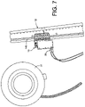
- FIG. 7 illustrates another view of the example connector of FIG. 1 as coupled to the example bus bar.
- FIG. 8 illustrates another view of the example connector of FIG. 1 as coupled to the example bus bar.
- FIG. 9 illustrates yet another view of the example connector of FIG. 1 as coupled to the example bus bar.
- FIG. 10 illustrates a further example connector.
- FIG. 11 illustrates a still further example connector.
- FIG. 12 illustrates a block diagram of example PCB components for use with the example connectors.
- FIG. 13 illustrates a yet further example connector.
- FIG. 14 illustrates the connector of FIG. 13 as coupled to the example bus bar.
- a connector 10 for use in electrically coupling a device, such as a power source device or a power sink device, to a bus bar will now be described.
- the exemplary connector 10 is especially adapted for use with a bus bar 12 of the type described in U.S. Pat. Nos. 8,062,042 and 7,997,910, i.e., a bus bar having a top portion where one side surface of the top portion carries a first conductive strip 14 A and the opposite side surface of the top portion carries a second conductive strip 14 B and wherein the first conductive strip 14 A and the second conductive strip 14 B have opposite polarities.
- the bottom portion of the bus bar may also be provided with conductive elements for providing direct current (DC power).
- FIGS. 6-9 illustrate the connector 10 being usable with a bus bar 12 of the noted type, it is to be understood that the hereinafter described connector 10 can be provided with other shapes, sizes, and/or arrangements as needed to thereby allow the connector 10 to be usable with other types of bus bars. Accordingly, the exemplary use environment that is illustrated in FIGS. 6-9 is not intended to be limiting.
- the connector 10 is provided with a pair of pivotally connected and optionally lockable electrical conductor housing elements 16 A and 16 B.
- a cap 16 C, 16 C′ may optionally be provided on at least one of the housings 16 A, 16 B if desired, but it will be appreciated that the housings 16 A, 16 B may be integrally formed without the cap 16 C, 16 C′ as desired.
- each of the housing elements 16 A and 16 B carries an electrical conductor 18 having a first end 20 and a second end (not shown).
- each electrical conductor 18 is arranged in its housing element 16 A and 16 B such that the first end of each of the electrical conductors 18 will be placed into engagement with a corresponding one of the conductive strips 14 A and 14 B when the connector 10 is, in turn, coupled to the bus bar 12 .
- the cooperating housing elements 16 A and 16 B will function to drive the first end 20 of each conductor 18 into a corresponding one of the conductive strips 14 A and 14 B.
- the second end of the electrical conductor 18 is arranged to be operatively coupled directly or indirectly to at least one of a printed circuit board 23 (PCB 23 ), or an external electrical conductor, such as a wire from a sink or source device.
- the conductors 18 are directly coupled to the PCB 23 at the second end as in any suitable manner as is known to one of ordinary skill in the art.
- the housing elements 16 A and 16 B may be provided with bus bar engaging surfaces 50 for preventing the connector 10 from being lifted off of the bus bar 12 .
- the second housing section 16 A is enlarged and/or otherwise elongated and sized (particularly relative to first housing section 16 B) to house the PCB 23 (see FIG. 4 ) and the PCB 23 is electrically coupled to the electrical conductors 18 .
- the PCB 23 includes relevant circuitry, including for instance power control, dimming control, transceiver capabilities, emergency power switching control, etc.
- the PCB 23 further includes, or is coupled to, at least one terminal for coupling to an external conductor, such as a wire, where the external conductor is fed through, or the terminal placed in, an aperture 29 formed by, in this example, the housing 16 A.
- the PCB 23 is coupled to terminals in an amount sufficient to allow the PCB 23 to be coupled to an emergency power source 1201 , the DC power grid bus power source 1203 , and a load device 1205 , such as a LED light fixture, as particularly illustrated in FIG. 12 .
- the housing may be provided with terminals (or apertures leading to terminals) as required to allow the PCB 23 to be coupled to the relevant electrical components as illustrated in FIGS.
- terminals 1101 provides a load-side power interface while terminals 1103 and/or 1003 provide a pulse width modulated (“PWM”) signal for the load to be coupled to the PCB 23 , a terminal 1003 for allowing conductor(s) that output a PWM signal for the load (or full power in the case when the PWM is lost) to be coupled to the PCB 23 , a terminal 1005 for allowing conductor(s) that function to provide DC emergency power to be coupled to the PCB 23 , a terminal 1101 for allowing conductor(s) that function to provide power, e.g., ON/OFF, to the load to be coupled to the PCB 23 , and/or a terminal 1103 for allowing conductor(s) that function to provide dimming control signals, e.g., 0-10 dimming, to the load to be coupled to the PCB 23 .
- terminals 1101 provides a load-side power interface while terminals 1103 and/or 1003 provide a
- the aperture 29 shown in FIGS. 6-9 is sized and configured to accept a push-in type electrical connector 35 , such as a “POWERPLUG® Luminaire Disconnects -180 Series” available from IDEAL INDUSTRIES, INC., or other electrical device. It will be appreciated that other types of wire connection terminations may also be used for this purpose, such as crimp type terminations, solder type terminations, or the like without limitation.
- a push-in type electrical connector 35 such as a “POWERPLUG® Luminaire Disconnects -180 Series” available from IDEAL INDUSTRIES, INC., or other electrical device.
- wire connection terminations may also be used for this purpose, such as crimp type terminations, solder type terminations, or the like without limitation.
- the electrical conductors 18 can function to provide an electrical coupling between wires of a device 37 (as coupled to the PCB 23 and/or the second end of the electrical conductors 18 ) and the conductive strips 14 A and 14 B of the bus bar 12 (as coupled to the first end 20 of the electrical conductors 18 ).
- the housing elements 16 A and 16 B are identically constructed and formed from an electrically insulating material while the electrical conductors 18 are formed using a resilient, electrically conductive material.
- the PCB 23 may also allow specialized control of the power and/or signal delivered to the device 37 , such as for instance a pulse-width modulation (PWM) dimming signal, a 0-10 diming signal, Digital Addressable Lighting Interface (DALI) protocol signal, or the like without limitation.
- PWM pulse-width modulation
- DALI Digital Addressable Lighting Interface
- the housing elements 16 A is provided with the cap 29 .
- the cap 16 C defines an aperture 29 , for receiving an electrical connector or an electrical conductor as desired.
- the cap 16 C is provided with a pair of locking elements 30 , e.g., one of a tang or a slot, while the housing element 16 A is provided with a pair of cooperating locking elements 32 , e.g., the other of a tang or a slot, to thereby allow the cap 16 A to be snap fit into engagement with the housing element 16 A and to thereby support the PCB 23 and the electrical contacts 18 from the top while locking the PCB 23 and the electrical contacts 18 in position within the housing element 16 A.
- Other locking type elements can also be used for this purpose and/or the cap 16 C can be secured to the housing element 16 A via use of other known methods such as welding, gluing, or the like.
- the housing sections 16 A and 16 B are each provided with a pivot post 34 and a pivot post receiving opening 36 that is axially aligned with the pivot post 34 .
- the pivot posts 34 is preferably integrally formed with its respective housing section 16 A and 16 B, but can be a separate element attached thereto as desired.
- the pivot post 34 of the housing section 16 A is intended to be received in the pivot post receiving opening 36 of the housing section 16 B.
- the connector 10 and more particularly housing sections 16 A and 16 B, are squeezed together (i.e., are moved in the direction shown by the lines C of FIG. 1 ) such that the pivot posts 34 of the housing sections 16 A and 16 B are moved into the pivot post receiving openings 36 of the opposite one of the housing sections 16 A and 16 B.
- the housing sections 16 A, 16 B may be biased into a closed position by any suitable means, including an external biasing member (e.g., a spring) or via construction shape of the housing and/or pivot posts 34 .
- the connector 10 can be locked to the bus bar 12 by rotating the housing sections 16 A and 16 B towards one another in the direction of the arrow C-C.
- the exemplary connector 10 includes a processing device 1201 which is electrically coupled to a DC power grid bus via use of a polarity reversing circuit 1202 (as needed).
- the DC power grid bus functions to provide DC power to the exemplary connector 10 .
- the exemplary connector 10 is further electrically coupled to a load device 1205 via use of a load-side power interface 1206 .
- the load-side power interface 1206 functions to provide DC power to the load device 1205 , which DC power may be on/off power and/or PWM dimmed power.
- the processing device 1201 may also function to provide a dimming control signal, e.g., a 0-10 dimming control signal, to the load device 1205 .
- the exemplary connector 10 may also be electrically coupled to an emergency power input 1201 .
- the connector 10 may function to provide power from the emergency power input 1201 to the load device, preferably to turn the load device 1205 full on.
- the example connector 10 may include a wireless transceiver 1209 wherein the wireless transceiver is used to provide a control signal—received from a further device—to the processing device 1201 for use in controlling operations of the connector 10 , e.g., to control power on/off, to control dimming, etc.
- the connector 10 may allow for state data associated with the connector 10 , and accordingly the device 1205 , and/or other data to be communicated to other remotely located devices as needed.
- FIGS. 13 and 14 a further exemplary connector 1300 , having a housing for housing the PCB 23 , which is adapted to be releasably connected to the underside of the bus bar 12 is illustrated.
- the connector 1300 includes an oblong shaped protuberance 1302 having electrical contacts 1304 for engaging with corresponding electrical conductors that are carried within a channel 13 of the bus bar 12 .
- the protuberance 1302 is aligned with and positioned within the channel 13 of the bus bar 12 and the connector 1300 is then twisted such that the underside of the ends located at the longest opposed sides of the protuberance 1302 rest upon corresponding channel rail edges 13 A that are provide to the bus bar 12 .
- the electrical contacts 1304 will be placed into electrical contact with the power conductors 13 B that are provided along the sides of the channel 13 .
- the connector 1300 may further be provided with seating elements 1306 , which may take the form of spring biased, ball shaped elements as illustrated, where the seating elements 1306 are arranged to be positioned within the channel 13 when the connector 1300 is placed into electrical connection with the bus bar 12 with the seating elements 1306 then functioning to inhibit the connector 1300 from being twisted to a point where such electrical connection is lost.
- the connector 1300 further includes a wire or other element 1308 by which a load device, such as a lamp, is mechanically connected to, e.g., hung from, the connector 1300 .
- the load device will also be electrically coupled to the connector 1300 , and accordingly PCB 23 , via use of wires 1310 as also illustrated.
Landscapes
- Engineering & Computer Science (AREA)
- General Engineering & Computer Science (AREA)
- Details Of Connecting Devices For Male And Female Coupling (AREA)
- Power Engineering (AREA)
- Coupling Device And Connection With Printed Circuit (AREA)
Abstract
Description
Claims (22)
Priority Applications (1)
| Application Number | Priority Date | Filing Date | Title |
|---|---|---|---|
| US15/485,725 US11353198B2 (en) | 2012-03-02 | 2017-04-12 | Electrical connector having a printed circuit board for use with an active grid bus bar system |
Applications Claiming Priority (8)
| Application Number | Priority Date | Filing Date | Title |
|---|---|---|---|
| US201261606129P | 2012-03-02 | 2012-03-02 | |
| US13/591,371 US20130229067A1 (en) | 2012-03-02 | 2012-08-22 | Connector having wireless control capabilities |
| US13/650,757 US9660447B2 (en) | 2012-03-02 | 2012-10-12 | Connector having wireless control capabilities |
| US201361812070P | 2013-04-15 | 2013-04-15 | |
| US201361812548P | 2013-04-16 | 2013-04-16 | |
| US14/226,017 US9627928B2 (en) | 2012-03-02 | 2014-03-26 | Electrical outlet having wireless control capabilities |
| US201662325827P | 2016-04-21 | 2016-04-21 | |
| US15/485,725 US11353198B2 (en) | 2012-03-02 | 2017-04-12 | Electrical connector having a printed circuit board for use with an active grid bus bar system |
Related Parent Applications (2)
| Application Number | Title | Priority Date | Filing Date |
|---|---|---|---|
| US13/650,757 Continuation-In-Part US9660447B2 (en) | 2012-03-02 | 2012-10-12 | Connector having wireless control capabilities |
| US14/226,017 Continuation-In-Part US9627928B2 (en) | 2012-03-02 | 2014-03-26 | Electrical outlet having wireless control capabilities |
Publications (2)
| Publication Number | Publication Date |
|---|---|
| US20170338572A1 US20170338572A1 (en) | 2017-11-23 |
| US11353198B2 true US11353198B2 (en) | 2022-06-07 |
Family
ID=60330952
Family Applications (1)
| Application Number | Title | Priority Date | Filing Date |
|---|---|---|---|
| US15/485,725 Active 2036-06-17 US11353198B2 (en) | 2012-03-02 | 2017-04-12 | Electrical connector having a printed circuit board for use with an active grid bus bar system |
Country Status (1)
| Country | Link |
|---|---|
| US (1) | US11353198B2 (en) |
Families Citing this family (2)
| Publication number | Priority date | Publication date | Assignee | Title |
|---|---|---|---|---|
| USD840350S1 (en) * | 2016-04-25 | 2019-02-12 | Ideal Industries, Inc. | Electrical connector for a grid bus bar system |
| JP6944614B2 (en) * | 2018-08-03 | 2021-10-06 | ウォーカー マイロンWALKER, Myron | Flexible and cutable radial bath and bus mount bead device |
Citations (19)
| Publication number | Priority date | Publication date | Assignee | Title |
|---|---|---|---|---|
| US6246182B1 (en) * | 1999-06-25 | 2001-06-12 | Matsushita Electric Works, Ltd. | Electronic track lighting system |
| US20030001506A1 (en) | 2001-05-28 | 2003-01-02 | Leleve Joel | Device connecting a lamp in a motor vehicle |
| US20050169015A1 (en) * | 2003-09-18 | 2005-08-04 | Luk John F. | LED color changing luminaire and track light system |
| US20050243549A1 (en) * | 2002-03-13 | 2005-11-03 | Ruston Joseph H | Remote position control of lighting unit |
| US20070291433A1 (en) | 2006-06-16 | 2007-12-20 | American Power Conversion Corporation | Apparatus and method for scalable power distribution |
| US20080001551A1 (en) | 2003-07-02 | 2008-01-03 | S.C. Johnson & Son, Inc. | Adapter for Light Bulbs Equipped with Volatile Active Dispenser and Light Emitting Diodes |
| US7997910B2 (en) | 2008-04-15 | 2011-08-16 | Awi Licensing Company | Connectors for electrically active grid |
| US8062042B2 (en) | 2008-12-19 | 2011-11-22 | Worthington Armstrong Venture | Internal bus bar and an electrical interconnection means therefor |
| US20120007516A1 (en) * | 2010-06-09 | 2012-01-12 | Lax Daniel A | Led task lighting system |
| WO2013130432A1 (en) | 2012-03-02 | 2013-09-06 | Ideal Industries, Inc. | Connector having wireless control capabilities |
| US20130323950A1 (en) * | 2012-06-01 | 2013-12-05 | Tyco Electronics Corporation | Connector assembly with polarity correction/protection |
| US20140217906A1 (en) * | 2013-02-01 | 2014-08-07 | Vung Van Vo | Remote Control Track Light Fixture |
| US20140308828A1 (en) | 2012-10-18 | 2014-10-16 | Facebook, Inc. | Floating bus bar and connector within chassis and powered slide rails |
| US8986021B2 (en) | 2012-03-09 | 2015-03-24 | Ideal Industries, Inc. | Connector having a push-in termination for an electrically active grid |
| US20150092449A1 (en) | 2013-10-02 | 2015-04-02 | Cree, Inc. | Modular driver module for light fixtures with led luminaires |
| US20150137683A1 (en) * | 2012-06-13 | 2015-05-21 | Soraa, Inc. | Led lamps and controllers for lighting fixtures |
| CN104704590A (en) | 2012-10-12 | 2015-06-10 | 理想工业公司 | Connector having wireless control capabilities |
| US9190790B1 (en) | 2014-07-10 | 2015-11-17 | Ideal Industries, Inc. | Electrical connector for use with a bus bar system |
| US9644828B1 (en) * | 2016-02-09 | 2017-05-09 | Michael W. May | Networked LED lighting system |
-
2017
- 2017-04-12 US US15/485,725 patent/US11353198B2/en active Active
Patent Citations (21)
| Publication number | Priority date | Publication date | Assignee | Title |
|---|---|---|---|---|
| US6246182B1 (en) * | 1999-06-25 | 2001-06-12 | Matsushita Electric Works, Ltd. | Electronic track lighting system |
| US20030001506A1 (en) | 2001-05-28 | 2003-01-02 | Leleve Joel | Device connecting a lamp in a motor vehicle |
| US20050243549A1 (en) * | 2002-03-13 | 2005-11-03 | Ruston Joseph H | Remote position control of lighting unit |
| US20080001551A1 (en) | 2003-07-02 | 2008-01-03 | S.C. Johnson & Son, Inc. | Adapter for Light Bulbs Equipped with Volatile Active Dispenser and Light Emitting Diodes |
| US20050169015A1 (en) * | 2003-09-18 | 2005-08-04 | Luk John F. | LED color changing luminaire and track light system |
| US20070291433A1 (en) | 2006-06-16 | 2007-12-20 | American Power Conversion Corporation | Apparatus and method for scalable power distribution |
| US7997910B2 (en) | 2008-04-15 | 2011-08-16 | Awi Licensing Company | Connectors for electrically active grid |
| US8062042B2 (en) | 2008-12-19 | 2011-11-22 | Worthington Armstrong Venture | Internal bus bar and an electrical interconnection means therefor |
| US20120007516A1 (en) * | 2010-06-09 | 2012-01-12 | Lax Daniel A | Led task lighting system |
| CN104160564A (en) | 2012-03-02 | 2014-11-19 | 理想工业公司 | Connector having wireless control capabilities |
| WO2013130432A1 (en) | 2012-03-02 | 2013-09-06 | Ideal Industries, Inc. | Connector having wireless control capabilities |
| US8986021B2 (en) | 2012-03-09 | 2015-03-24 | Ideal Industries, Inc. | Connector having a push-in termination for an electrically active grid |
| US8770993B2 (en) * | 2012-06-01 | 2014-07-08 | Tyco Electronics Corporation | Connector assembly with polarity correction/protection |
| US20130323950A1 (en) * | 2012-06-01 | 2013-12-05 | Tyco Electronics Corporation | Connector assembly with polarity correction/protection |
| US20150137683A1 (en) * | 2012-06-13 | 2015-05-21 | Soraa, Inc. | Led lamps and controllers for lighting fixtures |
| CN104704590A (en) | 2012-10-12 | 2015-06-10 | 理想工业公司 | Connector having wireless control capabilities |
| US20140308828A1 (en) | 2012-10-18 | 2014-10-16 | Facebook, Inc. | Floating bus bar and connector within chassis and powered slide rails |
| US20140217906A1 (en) * | 2013-02-01 | 2014-08-07 | Vung Van Vo | Remote Control Track Light Fixture |
| US20150092449A1 (en) | 2013-10-02 | 2015-04-02 | Cree, Inc. | Modular driver module for light fixtures with led luminaires |
| US9190790B1 (en) | 2014-07-10 | 2015-11-17 | Ideal Industries, Inc. | Electrical connector for use with a bus bar system |
| US9644828B1 (en) * | 2016-02-09 | 2017-05-09 | Michael W. May | Networked LED lighting system |
Non-Patent Citations (5)
| Title |
|---|
| CNIPA, office action issued on Chinese patent application No. 201710261453.3, 11 pages. |
| CNIPA, office action issued on Chinese patent application No. 201710261453.3, 5 pages. |
| European Patent Office, extended European search report issued on European patent application 17000694.4, dated Mar. 8, 2018, 11 pages. |
| European Patent Office, office action issued on European patent application No. 17000694.4, dated Apr. 12, 2021, 4 pages. |
| Wikipedia contributors. "Printed circuit board." Wikipedia, The Free Encyclopedia. Wikipedia, The Free Encyclopedia, Jul. 21, 2020. Web. Jul. 28, 2020. (Year: 2020). * |
Also Published As
| Publication number | Publication date |
|---|---|
| US20170338572A1 (en) | 2017-11-23 |
Similar Documents
| Publication | Publication Date | Title |
|---|---|---|
| US10024526B1 (en) | Connector for light-emitting diode strip | |
| US9660447B2 (en) | Connector having wireless control capabilities | |
| US9167660B2 (en) | Combined surface mount and in-wall mount dimmer | |
| US9239136B1 (en) | Connector for light-emitting diode strip | |
| US10636290B2 (en) | Communication interface device for a solid-state luminaire | |
| US9784441B2 (en) | Compact A.C. powered LED light fixture | |
| US20140062320A1 (en) | Lighting control circuit, lamp, and lighting control method using the lighting control circuit | |
| US11353198B2 (en) | Electrical connector having a printed circuit board for use with an active grid bus bar system | |
| WO2017153394A1 (en) | Socket assembly, light emitter module, and lighting system | |
| EP3273157B1 (en) | Led lamp electrical connection member | |
| US10923864B2 (en) | Overvoltage protection module for a modular plug connector | |
| WO2016090708A1 (en) | Dimming device and drive dimming device | |
| GB2582046A (en) | LED strip connector | |
| DE102018114619A1 (en) | terminal unit | |
| WO2003075126A3 (en) | One wire self referencing circuits for providing power and data | |
| CA2887153C (en) | Connector having wireless control capabilities | |
| EP3132182B1 (en) | Lamp device, led lamp, and luminaire | |
| EP3236560A2 (en) | Electrical connector having a printed circuit board for use with an active grid bus bar system | |
| EP2973885B1 (en) | Wireless connector node and system | |
| DE102017100413A1 (en) | Power supply, lighting system, lighting system and method for reducing the time required to extinguish an arc | |
| CN109728470B (en) | Tapping plug connector | |
| US9755386B2 (en) | Device for contacting electrical conductors and/or electrical contact elements, as well as lamp or electrical device | |
| CN205452057U (en) | Intelligent switch module | |
| CN212462275U (en) | Low-voltage power supply distribution box | |
| KR101610336B1 (en) | User selection type illuminating apparatus |
Legal Events
| Date | Code | Title | Description |
|---|---|---|---|
| AS | Assignment |
Owner name: IDEAL INDUSTRIES, INC., ILLINOIS Free format text: ASSIGNMENT OF ASSIGNORS INTEREST;ASSIGNORS:KESWANI, SUSHIL N.;TUNNELL, TIMOTHY B.;TAMMISTO, ADAM JAMES;REEL/FRAME:041995/0470 Effective date: 20170413 |
|
| STPP | Information on status: patent application and granting procedure in general |
Free format text: DOCKETED NEW CASE - READY FOR EXAMINATION |
|
| STPP | Information on status: patent application and granting procedure in general |
Free format text: RESPONSE TO NON-FINAL OFFICE ACTION ENTERED AND FORWARDED TO EXAMINER |
|
| STPP | Information on status: patent application and granting procedure in general |
Free format text: NON FINAL ACTION MAILED |
|
| STPP | Information on status: patent application and granting procedure in general |
Free format text: RESPONSE TO NON-FINAL OFFICE ACTION ENTERED AND FORWARDED TO EXAMINER |
|
| STPP | Information on status: patent application and granting procedure in general |
Free format text: RESPONSE TO NON-FINAL OFFICE ACTION ENTERED AND FORWARDED TO EXAMINER |
|
| STPP | Information on status: patent application and granting procedure in general |
Free format text: FINAL REJECTION MAILED |
|
| STPP | Information on status: patent application and granting procedure in general |
Free format text: RESPONSE AFTER FINAL ACTION FORWARDED TO EXAMINER |
|
| STPP | Information on status: patent application and granting procedure in general |
Free format text: ADVISORY ACTION MAILED |
|
| STPP | Information on status: patent application and granting procedure in general |
Free format text: NON FINAL ACTION MAILED |
|
| STPP | Information on status: patent application and granting procedure in general |
Free format text: RESPONSE TO NON-FINAL OFFICE ACTION ENTERED AND FORWARDED TO EXAMINER |
|
| STPP | Information on status: patent application and granting procedure in general |
Free format text: NON FINAL ACTION MAILED |
|
| STPP | Information on status: patent application and granting procedure in general |
Free format text: NOTICE OF ALLOWANCE MAILED -- APPLICATION RECEIVED IN OFFICE OF PUBLICATIONS |
|
| STPP | Information on status: patent application and granting procedure in general |
Free format text: PUBLICATIONS -- ISSUE FEE PAYMENT VERIFIED |
|
| STCF | Information on status: patent grant |
Free format text: PATENTED CASE |
|
| AS | Assignment |
Owner name: JPMORGAN CHASE BANK, N.A., AS ADMINISTRATIVE AGENT, ILLINOIS Free format text: SECURITY INTEREST;ASSIGNORS:IDEAL INDUSTRIES, INC.;ANDERSON POWER PRODUCTS, INC.;REEL/FRAME:066358/0354 Effective date: 20240119 |