US11316303B2 - High frequency connector with component protecting member and method of manufacturing thereof - Google Patents

High frequency connector with component protecting member and method of manufacturing thereof Download PDF

Info

Publication number
US11316303B2
US11316303B2 US16/677,466 US201916677466A US11316303B2 US 11316303 B2 US11316303 B2 US 11316303B2 US 201916677466 A US201916677466 A US 201916677466A US 11316303 B2 US11316303 B2 US 11316303B2
Authority
US
United States
Prior art keywords
circuit board
protecting member
cable
component
high frequency
Prior art date
Legal status (The legal status is an assumption and is not a legal conclusion. Google has not performed a legal analysis and makes no representation as to the accuracy of the status listed.)
Active, expires
Application number
US16/677,466
Other versions
US20200328561A1 (en
Inventor
Shih Yao Chiang
Chieh-Ming Cheng
Current Assignee (The listed assignees may be inaccurate. Google has not performed a legal analysis and makes no representation or warranty as to the accuracy of the list.)
Jess Link Products Co Ltd
Original Assignee
Jess Link Products Co Ltd
Priority date (The priority date is an assumption and is not a legal conclusion. Google has not performed a legal analysis and makes no representation as to the accuracy of the date listed.)
Filing date
Publication date
Application filed by Jess Link Products Co Ltd filed Critical Jess Link Products Co Ltd
Assigned to JESS-LINK PRODUCTS CO., LTD. reassignment JESS-LINK PRODUCTS CO., LTD. ASSIGNMENT OF ASSIGNORS INTEREST (SEE DOCUMENT FOR DETAILS). Assignors: CHENG, CHIEH-MING
Publication of US20200328561A1 publication Critical patent/US20200328561A1/en
Application granted granted Critical
Publication of US11316303B2 publication Critical patent/US11316303B2/en
Active legal-status Critical Current
Adjusted expiration legal-status Critical

Links

Images

Classifications

    • HELECTRICITY
    • H05ELECTRIC TECHNIQUES NOT OTHERWISE PROVIDED FOR
    • H05KPRINTED CIRCUITS; CASINGS OR CONSTRUCTIONAL DETAILS OF ELECTRIC APPARATUS; MANUFACTURE OF ASSEMBLAGES OF ELECTRICAL COMPONENTS
    • H05K3/00Apparatus or processes for manufacturing printed circuits
    • H05K3/30Assembling printed circuits with electric components, e.g. with resistor
    • H05K3/301Assembling printed circuits with electric components, e.g. with resistor by means of a mounting structure
    • HELECTRICITY
    • H01ELECTRIC ELEMENTS
    • H01RELECTRICALLY-CONDUCTIVE CONNECTIONS; STRUCTURAL ASSOCIATIONS OF A PLURALITY OF MUTUALLY-INSULATED ELECTRICAL CONNECTING ELEMENTS; COUPLING DEVICES; CURRENT COLLECTORS
    • H01R13/00Details of coupling devices of the kinds covered by groups H01R12/70 or H01R24/00 - H01R33/00
    • H01R13/646Details of coupling devices of the kinds covered by groups H01R12/70 or H01R24/00 - H01R33/00 specially adapted for high-frequency, e.g. structures providing an impedance match or phase match
    • HELECTRICITY
    • H01ELECTRIC ELEMENTS
    • H01RELECTRICALLY-CONDUCTIVE CONNECTIONS; STRUCTURAL ASSOCIATIONS OF A PLURALITY OF MUTUALLY-INSULATED ELECTRICAL CONNECTING ELEMENTS; COUPLING DEVICES; CURRENT COLLECTORS
    • H01R12/00Structural associations of a plurality of mutually-insulated electrical connecting elements, specially adapted for printed circuits, e.g. printed circuit boards [PCB], flat or ribbon cables, or like generally planar structures, e.g. terminal strips, terminal blocks; Coupling devices specially adapted for printed circuits, flat or ribbon cables, or like generally planar structures; Terminals specially adapted for contact with, or insertion into, printed circuits, flat or ribbon cables, or like generally planar structures
    • H01R12/50Fixed connections
    • H01R12/51Fixed connections for rigid printed circuits or like structures
    • H01R12/53Fixed connections for rigid printed circuits or like structures connecting to cables except for flat or ribbon cables
    • HELECTRICITY
    • H01ELECTRIC ELEMENTS
    • H01RELECTRICALLY-CONDUCTIVE CONNECTIONS; STRUCTURAL ASSOCIATIONS OF A PLURALITY OF MUTUALLY-INSULATED ELECTRICAL CONNECTING ELEMENTS; COUPLING DEVICES; CURRENT COLLECTORS
    • H01R13/00Details of coupling devices of the kinds covered by groups H01R12/70 or H01R24/00 - H01R33/00
    • H01R13/46Bases; Cases
    • HELECTRICITY
    • H01ELECTRIC ELEMENTS
    • H01RELECTRICALLY-CONDUCTIVE CONNECTIONS; STRUCTURAL ASSOCIATIONS OF A PLURALITY OF MUTUALLY-INSULATED ELECTRICAL CONNECTING ELEMENTS; COUPLING DEVICES; CURRENT COLLECTORS
    • H01R43/00Apparatus or processes specially adapted for manufacturing, assembling, maintaining, or repairing of line connectors or current collectors or for joining electric conductors
    • H01R43/02Apparatus or processes specially adapted for manufacturing, assembling, maintaining, or repairing of line connectors or current collectors or for joining electric conductors for soldered or welded connections
    • H01R43/0256Apparatus or processes specially adapted for manufacturing, assembling, maintaining, or repairing of line connectors or current collectors or for joining electric conductors for soldered or welded connections for soldering or welding connectors to a printed circuit board
    • HELECTRICITY
    • H05ELECTRIC TECHNIQUES NOT OTHERWISE PROVIDED FOR
    • H05KPRINTED CIRCUITS; CASINGS OR CONSTRUCTIONAL DETAILS OF ELECTRIC APPARATUS; MANUFACTURE OF ASSEMBLAGES OF ELECTRICAL COMPONENTS
    • H05K1/00Printed circuits
    • H05K1/02Details
    • H05K1/11Printed elements for providing electric connections to or between printed circuits
    • H05K1/111Pads for surface mounting, e.g. lay-out
    • HELECTRICITY
    • H05ELECTRIC TECHNIQUES NOT OTHERWISE PROVIDED FOR
    • H05KPRINTED CIRCUITS; CASINGS OR CONSTRUCTIONAL DETAILS OF ELECTRIC APPARATUS; MANUFACTURE OF ASSEMBLAGES OF ELECTRICAL COMPONENTS
    • H05K3/00Apparatus or processes for manufacturing printed circuits
    • H05K3/30Assembling printed circuits with electric components, e.g. with resistor
    • H05K3/32Assembling printed circuits with electric components, e.g. with resistor electrically connecting electric components or wires to printed circuits
    • H05K3/34Assembling printed circuits with electric components, e.g. with resistor electrically connecting electric components or wires to printed circuits by soldering
    • HELECTRICITY
    • H01ELECTRIC ELEMENTS
    • H01RELECTRICALLY-CONDUCTIVE CONNECTIONS; STRUCTURAL ASSOCIATIONS OF A PLURALITY OF MUTUALLY-INSULATED ELECTRICAL CONNECTING ELEMENTS; COUPLING DEVICES; CURRENT COLLECTORS
    • H01R12/00Structural associations of a plurality of mutually-insulated electrical connecting elements, specially adapted for printed circuits, e.g. printed circuit boards [PCB], flat or ribbon cables, or like generally planar structures, e.g. terminal strips, terminal blocks; Coupling devices specially adapted for printed circuits, flat or ribbon cables, or like generally planar structures; Terminals specially adapted for contact with, or insertion into, printed circuits, flat or ribbon cables, or like generally planar structures
    • H01R12/50Fixed connections
    • H01R12/59Fixed connections for flexible printed circuits, flat or ribbon cables or like structures
    • H01R12/62Fixed connections for flexible printed circuits, flat or ribbon cables or like structures connecting to rigid printed circuits or like structures
    • HELECTRICITY
    • H05ELECTRIC TECHNIQUES NOT OTHERWISE PROVIDED FOR
    • H05KPRINTED CIRCUITS; CASINGS OR CONSTRUCTIONAL DETAILS OF ELECTRIC APPARATUS; MANUFACTURE OF ASSEMBLAGES OF ELECTRICAL COMPONENTS
    • H05K1/00Printed circuits
    • H05K1/02Details
    • H05K1/11Printed elements for providing electric connections to or between printed circuits
    • H05K1/117Pads along the edge of rigid circuit boards, e.g. for pluggable connectors
    • HELECTRICITY
    • H05ELECTRIC TECHNIQUES NOT OTHERWISE PROVIDED FOR
    • H05KPRINTED CIRCUITS; CASINGS OR CONSTRUCTIONAL DETAILS OF ELECTRIC APPARATUS; MANUFACTURE OF ASSEMBLAGES OF ELECTRICAL COMPONENTS
    • H05K2201/00Indexing scheme relating to printed circuits covered by H05K1/00
    • H05K2201/09Shape and layout
    • H05K2201/09009Substrate related
    • H05K2201/09063Holes or slots in insulating substrate not used for electrical connections
    • HELECTRICITY
    • H05ELECTRIC TECHNIQUES NOT OTHERWISE PROVIDED FOR
    • H05KPRINTED CIRCUITS; CASINGS OR CONSTRUCTIONAL DETAILS OF ELECTRIC APPARATUS; MANUFACTURE OF ASSEMBLAGES OF ELECTRICAL COMPONENTS
    • H05K2201/00Indexing scheme relating to printed circuits covered by H05K1/00
    • H05K2201/09Shape and layout
    • H05K2201/09209Shape and layout details of conductors
    • H05K2201/09372Pads and lands
    • H05K2201/09409Multiple rows of pads, lands, terminals or dummy patterns; Multiple rows of mounted components
    • HELECTRICITY
    • H05ELECTRIC TECHNIQUES NOT OTHERWISE PROVIDED FOR
    • H05KPRINTED CIRCUITS; CASINGS OR CONSTRUCTIONAL DETAILS OF ELECTRIC APPARATUS; MANUFACTURE OF ASSEMBLAGES OF ELECTRICAL COMPONENTS
    • H05K2201/00Indexing scheme relating to printed circuits covered by H05K1/00
    • H05K2201/10Details of components or other objects attached to or integrated in a printed circuit board
    • H05K2201/10227Other objects, e.g. metallic pieces
    • H05K2201/10356Cables
    • HELECTRICITY
    • H05ELECTRIC TECHNIQUES NOT OTHERWISE PROVIDED FOR
    • H05KPRINTED CIRCUITS; CASINGS OR CONSTRUCTIONAL DETAILS OF ELECTRIC APPARATUS; MANUFACTURE OF ASSEMBLAGES OF ELECTRICAL COMPONENTS
    • H05K2201/00Indexing scheme relating to printed circuits covered by H05K1/00
    • H05K2201/10Details of components or other objects attached to or integrated in a printed circuit board
    • H05K2201/10227Other objects, e.g. metallic pieces
    • H05K2201/10393Clamping a component by an element or a set of elements
    • HELECTRICITY
    • H05ELECTRIC TECHNIQUES NOT OTHERWISE PROVIDED FOR
    • H05KPRINTED CIRCUITS; CASINGS OR CONSTRUCTIONAL DETAILS OF ELECTRIC APPARATUS; MANUFACTURE OF ASSEMBLAGES OF ELECTRICAL COMPONENTS
    • H05K2201/00Indexing scheme relating to printed circuits covered by H05K1/00
    • H05K2201/10Details of components or other objects attached to or integrated in a printed circuit board
    • H05K2201/10431Details of mounted components
    • H05K2201/10507Involving several components
    • H05K2201/10522Adjacent components

Definitions

  • the present invention relates to a high frequency component protecting member, more particularly, to a high frequency component protecting member applied to the high frequency connector and capable of maintaining the signal transmission characteristics of high frequency electronic components.
  • Connectors are connecting components and accessories for electrical signals, and the electronic devices translate and transmit the signal to each other through the cables and connectors. That is to say, the connectors are the communicating bridges for the signals.
  • the connectors are widely applied on cars and computer peripheral and communicating data applications, industries, military and aerospace industry, transportation, consumer electronics, medical treatments, instruments, commercial equipment and so on. Therefore, the connectors play an important role in many fields. In this well developed and efficient generation, the transmission speed of the signal is being developed toward high speed continuously. The high frequency connectors also have been developed to increase the transmission speed of the signal.
  • the signal attenuation is a problem when transmitting the signals in high frequency bands.
  • the signal attenuation includes conductive loss and dielectric loss, and the degree of the signal attenuation is enhanced by the increased distance. Therefore, the signal transmitting distance of the connector will decrease due to the signal attenuation.
  • the medium covering the high frequency electronic component and the circuit layout on the circuit board directly affects the signal transmission characteristics when designing the circuit of high frequency connectors.
  • the circuit boards, electronic components, and wires in the connector become more and more fine. Due to the limitations and the versatile requirements of the circuit board, some of the solder pads must be configured on the non-edge positions of the circuit board. It means that some of the wires must be configured across the high frequency electronic components.
  • the insulation glue or other similar fixing material would be pasted between the wires and the circuit board to make the wires across the high frequency electronic component and connect the circuit board by the insulation glue.
  • the insulation glue also covers the high frequency electronic component on the circuit board, which causes the dielectric coefficient around the high frequency electronic component to become greater and to increase the dielectric loss, so as to seriously affects the signal transmission characteristics.
  • a category of the present invention is to provide a high frequency connector, which can protect the high frequency electronic components on the circuit board and maintain the signal transmission characteristics.
  • the high frequency connector includes a case, a circuit board, a component protecting member and a cable.
  • the circuit board is configured in the case and has an electronic component and a plurality of solder pads disposed thereon.
  • the component protecting member includes a case body and is configured on the circuit board. One side of the case body has an opening. A containing space is formed by the opening and an inner surface of the case body, and a crossing structure is disposed on an outer surface of the other side of the case body.
  • the electronic component of the circuit is contained in the containing space.
  • the cable includes an insulating part and a conductive part disposed on the terminal of the cable. The insulating part of the cable is configured on the crossing structure, and the conductive part of the cable is soldered on the solder pads of the circuit board.
  • the circuit board further includes at least one positioning hole, and the component protecting member includes at least one positioning pin.
  • the size of the at least one positioning pin is corresponding to that of the positioning hole.
  • the maximum height of the containing space is greater than that of the electronic component to prevent the electronic component from contacting the inner surface of the case body.
  • the shape of the crossing structure is one selected from the group consisting of a circular arc shape, a polygonal shape and a combination of both.
  • the crossing structure further includes at least one groove, and the cable is configured in the groove.
  • the high frequency connector further includes a colloid pasted on the cable and the circuit board, and the component protecting member blocks the colloid out of the containing space.
  • Another one category of the present invention is to provide a method for manufacturing the high frequency connector.
  • the method includes the following steps of: soldering a conductive part of a first cable on a first pad of a circuit board; disposing a component protecting member on the circuit board to make the component protecting member to cover an electronic component of the circuit board; configuring a second cable across the component protecting member and soldering the second cable on a second solder pad of the circuit board; pasting a colloid on the first solder pad and the second solder pad of the circuit board; and disposing the circuit board, the component protecting member, the first cable and the second cable in a case.
  • the step of disposing a component protecting member on the circuit board to make the component protecting member to cover an electronic component of the circuit board further includes the step of: inserting at least one positioning pin of the component protecting member into at least one positioning hole of the circuit board correspondingly to make a containing space of the component protecting member to contain the electronic component.
  • the step of configuring a second cable across the component protecting member and soldering the second cable on a second solder pad of the circuit board further includes the step of: configuring the insulating part of the second cable on the crossing structure of the component protecting member, and soldering the conductive part of the second cable on the second solder pad of the circuit board.
  • the step of configuring a second cable across the component protecting member and soldering the second cable on a second solder pad of the circuit board further includes the step of: configuring the second cable in at least one groove of the component protecting member and soldering the second cable on the second solder pad of the circuit board.
  • the high frequency connector of the present invention ensures that the electronic component can contact with dielectric medium well to maintain the transmission characteristic of the electronic component by the component protecting member covering the electronic component and the corresponding circuit.
  • FIG. 1 is an exploded diagram illustrating a high frequency connector according to one embodiment of the present invention.
  • FIG. 2 is a structural schematic diagram illustrating the component protecting member of FIG. 1 .
  • FIG. 3 is an assembly schematic diagram illustrating the circuit board and the component protecting member of FIG. 1 .
  • FIG. 4 is a schematic diagram illustrating the circuit board and the component protecting member according to one embodiment of the present invention.
  • FIG. 5 is a schematic diagram illustrating the different shapes of the component protecting member according to another embodiment of the present invention.
  • FIG. 6A is a schematic diagram illustrating a high frequency connector according to another embodiment of the present invention.
  • FIG. 6B is a sectional diagram of the high frequency connector along the line A-A in FIG. 6A .
  • FIG. 7 is a schematic diagram illustrating the component protecting member according to another embodiment of the present invention.
  • FIG. 8 is an assembly schematic diagram illustrating the component protecting member and the circuit board of FIG. 7 .
  • FIG. 9 is a flow diagram illustrating a method for manufacturing the high frequency connector according to one embodiment of the present invention.
  • FIG. 10 is a flow diagram illustrating the method for manufacturing the high frequency connector according to one embodiment of the present invention.
  • FIG. 11 is a flow diagram illustrating the method for manufacturing the high frequency connector according to one embodiment of the present invention.
  • FIG. 12 is a flow diagram illustrating the method for manufacturing the high frequency connector according to another embodiment of the present invention.
  • FIG. 1 is an exploded diagram illustrating a high frequency connector 1 according to one embodiment of the present invention.
  • FIG. 2 is a structural schematic diagram illustrating the component protecting member 13 of FIG. 1 .
  • FIG. 3 is an assembly schematic diagram illustrating the circuit board 12 and the component protecting member 13 of FIG. 1 .
  • FIG. 4 is a schematic diagram illustrating the circuit board 12 and the component protecting member 13 according to one embodiment of the present invention.
  • the high frequency connector 1 of this embodiment includes a case 11 , a circuit board 12 , a component protecting member 13 and a cable 14 .
  • the circuit board 12 is configured in the case 11 and has a plurality of solder pads 127 and 128 , an electronic component 122 and at least two positioning holes 124 .
  • the component protecting member 13 includes a case body 131 and at least two positioning pins 132 extended from the case body 131 .
  • the component protecting member 13 can be configured on the circuit board 12 by the positioning pins 132 inserting into the positioning holes 124 of the circuit board 12 .
  • One side of the case 11 includes an opening, and the circuit board 12 can be inserted and configured in the case 11 through the opening of the case 11 .
  • one side of the case body 131 of the component protecting member 13 has an opening 134 .
  • a containing space 133 is formed by the opening 134 and the inner surface of the case body 131 , and a crossing structure 135 is disposed on the outer surface of the other side of the case body 131 .
  • the positioning pins 132 extend outward from the case body 131 .
  • the positioning pins 132 of this embodiment extend from the direction of the opening 134 of the case body 131 .
  • the position and shape of the positioning pins 132 are corresponding to those of the positioning holes 124 of the circuit board 12 , and the size of the positioning pins 132 can be slightly smaller than that of the positioning holes 124 .
  • the component protecting member 13 is disposed on the circuit board 12 through the positioning pins 132 inserting into the positioning holes 124 of the circuit board 12 .
  • the bottom plane on the side of the opening 134 of the case body 131 of the component protecting member 13 attaches to the circuit board 12 so that the containing space 133 contains the electronic component 122 on the circuit board 12 . That is to say, the component protecting member 13 covers the electronic component 122 on the circuit board 12 .
  • the electronic component 122 can be a high frequency transmitting or communicating electronic component.
  • the component protecting member 13 covers three electronic components 122 , but it is not limited to three in practice.
  • the number of the electronic component 122 can be 1, 2 or more than 3.
  • the positioning pins 132 of the component protecting member 13 in FIG. 2 are located on the same side and at the corners of the case body 131 , but it is not limited thereto. In another embodiment, the positioning pins 132 of the component protecting member 13 can be located at the opposite corners or non-corner positions of the case body 131 , which are corresponding to the positioning holes 124 of the circuit board 12 .
  • the shapes of the positioning pins 132 and the positioning holes 124 can be a circular shape or semi-circular shape (as shown in FIG.
  • the circuit board 12 has the positioning holes 124 with the corresponding positions and numbers to the positioning pins 132 .
  • the cable soldering positions of the connector are designed on the edge of the circuit board to prevent the cable from contacting the electronic component and affecting the transmission characteristic of the electronic component.
  • a first solder pad 127 is located on the edge of the circuit board 12 .
  • the first cable 141 can be soldered on the first solder pad 127 without contacting the electronic component when the conductive part 144 of the first cable 141 is soldered on the first solder pad 127 .
  • some of the cable soldering positions must be located on the non-edge positions of the circuit board under the situation of insufficient configuration space on the circuit board.
  • a second solder pad 128 is located among the electronic components 122 of the circuit board 12 .
  • the insulating part 143 of the second cable 142 would contact the electronic component 122 when the conductive part 144 of the second cable 142 is soldered on the second solder pad 128 .
  • the medium covering on the electronic component 122 of the circuit board 12 affects the signal transmission characteristics, such as transmitting speed, signal integrity and so on.
  • the dielectric constant of the electric component 122 is greater than 1 when the insulating part 143 of the second cable 142 contacts the electronic component 122 .
  • the transmission characteristic of the electronic component is affected, such as increasing the signal attenuation and reducing the transmission speed.
  • the component protecting member 13 when the component protecting member 13 is configured on the circuit board 12 , it can separate the electronic component 122 from the second cable to make the electronic component 122 not to contact the second cable 142 directly, and then maintain the transmission characteristic of the electronic component 122 .
  • the second cable 142 is configured on the crossing structure 135 of the component protecting member 13 when the second cable 142 is soldered on the second solder pad 128 , as shown in FIG. 4 . Therefore, the component protecting member 143 blocks the second cable 142 by the case body 131 and protects the electronic component 122 through the containing space 133 to ensure the optimum dielectric medium around the electronic component 122 , and then to maintain the transmission characteristic of the electronic component 122 .
  • the maximum height of the containing space 133 of the component protecting member 13 is greater than that of the electronic component 122 of the circuit board 12 .
  • the component protecting member 13 not only blocks the second cable 142 from the electronic component 122 , but also prevents the electronic component 122 from contacting the inner surface of the case body 131 of the component protecting member 13 , so as to ensure the optimum dielectric medium around the electronic component 122 to maintain the signal transmission characteristics of the electronic component 122 .
  • the component protecting member 13 is a curved sheet-like structure, but it is not limited thereto.
  • FIG. 5 is a schematic diagram illustrating the different shapes of the component protecting members 13 ′, 13 ′′, and 13 ′′′ according to another one embodiment of the present invention.
  • the shapes of the crossing structures 135 ′, 135 ′′, 135 ′′′ of the component protecting members 13 ′, 13 ′′, 13 ′′′ can also be a polygon (such as a trapezoid or polygon with lead angle) or a combination of circular arc shape and polygon (such as a polygon with arc lead angle).
  • the component protecting member 13 can include at least one rib configured at the inner surface of the case body to improve the structure strength of the component protecting member 13 .
  • FIG. 6A is a schematic diagram illustrating a high frequency connector 1 according to another embodiment of the present invention.
  • FIG. 6B is a sectional diagram of the high frequency connector 1 along the line A-A in FIG. 6A .
  • a colloid 15 is used to adhere and fix the conductive parts 144 of the first cable 141 and the second cable 142 to the first solder pad 127 and the second solder pad 128 of the circuit board 12 respectively after soldering the first cable 141 and the second cable 142 on the circuit board 12 .
  • the colloid 15 is further pasted on the insulating part 143 of the first cable 141 and the second cable 142 and the component protecting member 13 .
  • the colloid 15 fixes the first cable 141 , the second cable 142 and the component protecting member 13 on the circuit board 12 . It not only increases the holding strength of the first cable 141 and the second cable 142 and prevent the first cable 141 and the second cable 142 from being pulled off, but also prevents the component protecting member 13 from falling off.
  • the component protecting member 13 can exclude the colloid 15 from the containing space 133 when the colloid 15 is pasted on the circuit board 12 . Therefore, the electronic component 122 in the containing space 133 would not contact with the colloid 15 , so as to maintain the signal transmission characteristics.
  • the colloid 15 can be a waterproof glue or insulation glue.
  • the colloid 15 can be pasted on the circuit board 12 , also can be pasted between the circuit board 12 and case 11 to make the structure of high frequency connector become more stable.
  • FIG. 7 is a schematic diagram illustrating the component protecting member 23 according to another one embodiment of the present invention.
  • FIG. 8 is an assembly schematic diagram illustrating the component protecting member 23 and the circuit board 12 of FIG. 7 .
  • the difference between the above embodiment and this embodiment is that the case body 231 of the component protecting member 23 includes at least one groove 236 configured on the outer surface of the crossing structure 235 , so that the second cable 142 can be configured into each groove 236 when the component protecting member 23 is configured on the circuit board 12 .
  • the component protecting member 23 including the groove 236 not only makes the second cable 142 to be arranged neatly and less entangled, but also saves the space.
  • the number of the grooves 236 of the component protecting member 23 is four in FIG. 7 and FIG. 8 , but it is not limited thereto.
  • the number of the grooves 236 can be 1, 2, 3 or more than 4 to match that of the second cable 142 configured on the component protecting member 23 .
  • FIG. 9 is a flow diagram illustrating a method for manufacturing the high frequency connector according to one embodiment of the present invention.
  • the present invention also provides a method for manufacturing the high frequency connector including the following steps of: step S 1 : soldering a conductive part of a first cable on a first solder pad of a circuit board; step S 2 : disposing a component protecting member on the circuit board to make the component protecting member to cover a electronic component of the circuit board; step S 3 : configuring a second cable across the component protecting member and soldering the second cable on a second solder pad of the circuit board; step S 4 : pasting a colloid on the first solder pad and the second solder pad of the circuit board; and step S 5 : disposing the circuit board, the component protecting member, the first cable and the second cable in a case.
  • the method for manufacturing the high frequency connector shown in FIG. 9 can be achieved through the high frequency connector 1 shown in FIG. 1 and FIG. 4 .
  • the functions of the units mentioned in the steps of this embodiment are substantially the same as those of the corresponding units in the above embodiments, and thus will not be described herein. In practice, the sequence of step S 1 and step S 2 can be exchanged.
  • FIG. 10 is a flow diagram illustrating the method for manufacturing the high frequency connector according to one embodiment of the present invention.
  • Step S 2 further includes step S 21 : inserting at least two positioning pins of the component protecting member into at least two positioning holes of the circuit board correspondingly to make a containing space of the component protecting member to contain the electronic component.
  • FIG. 11 is a flow diagram illustrating the method for manufacturing the high frequency connector according to one embodiment of the present invention.
  • Step S 3 further includes step S 31 : configuring the insulating part of the second cable on the crossing structure of the component protecting member, and soldering the conductive part of the second cable on the second solder pad of the circuit board.
  • FIG. 12 is a flow diagram illustrating the method for manufacturing the high frequency connector according to another one embodiment of the present invention.
  • Step S 3 further includes step S 32 : configuring the second cable in at least one groove of the component protecting member and soldering the second cable on the second solder pad of the circuit board.
  • the high frequency connector of the present invention ensures that the electronic component contacts optimum dielectric medium to maintain the transmission characteristic of the electronic component by the component protecting member covering the electronic component on the circuit board.

Landscapes

  • Engineering & Computer Science (AREA)
  • Manufacturing & Machinery (AREA)
  • Microelectronics & Electronic Packaging (AREA)
  • Coupling Device And Connection With Printed Circuit (AREA)
  • Details Of Connecting Devices For Male And Female Coupling (AREA)

Abstract

A high frequency connector includes a case, a circuit board, a component protecting member and a cable. The circuit board is configured in the case and includes an electronic component and a plurality of solder pads. The component protecting member includes a case body and is configured on the circuit board. One side of the case body has an opening, and a containing space is formed between the opening and the inner face of the case body. A crossing structure is formed by the outer surface of the other side of the case body. When the component protecting member is configured on the circuit board, the component protecting member covers the electronic component in the containing space to maintain the transmission characteristics of the electronic component.

Description

CROSS-REFERENCE TO RELATED APPLICATION
This application claims priority to and the benefit of Taiwan Patent Application No. 108112322, filed on Apr. 9, 2019, the disclosure of which is incorporated herein by reference in its entirety.
BACKGROUND OF THE INVENTION 1. Field of the Invention
The present invention relates to a high frequency component protecting member, more particularly, to a high frequency component protecting member applied to the high frequency connector and capable of maintaining the signal transmission characteristics of high frequency electronic components.
2. Description of the Prior Art
Connectors are connecting components and accessories for electrical signals, and the electronic devices translate and transmit the signal to each other through the cables and connectors. That is to say, the connectors are the communicating bridges for the signals. The connectors are widely applied on cars and computer peripheral and communicating data applications, industries, military and aerospace industry, transportation, consumer electronics, medical treatments, instruments, commercial equipment and so on. Therefore, the connectors play an important role in many fields. In this well developed and efficient generation, the transmission speed of the signal is being developed toward high speed continuously. The high frequency connectors also have been developed to increase the transmission speed of the signal.
However, the signal attenuation is a problem when transmitting the signals in high frequency bands. The signal attenuation includes conductive loss and dielectric loss, and the degree of the signal attenuation is enhanced by the increased distance. Therefore, the signal transmitting distance of the connector will decrease due to the signal attenuation.
The medium covering the high frequency electronic component and the circuit layout on the circuit board directly affects the signal transmission characteristics when designing the circuit of high frequency connectors. In general, the optimum medium is air (dielectric constant, Dk=1). Therefore, the design of the circuit board in connector industry disposes the solder pads of the wires on the edge of the circuit board to avoid affecting the high frequency electronic component.
With the rapid development of technology, various electronic devices become lighter, thinner, shorter and smaller, and the circuit boards, electronic components, and wires in the connector become more and more fine. Due to the limitations and the versatile requirements of the circuit board, some of the solder pads must be configured on the non-edge positions of the circuit board. It means that some of the wires must be configured across the high frequency electronic components. In the prior art, in order to dispose the wires across the electronic components, the insulation glue or other similar fixing material would be pasted between the wires and the circuit board to make the wires across the high frequency electronic component and connect the circuit board by the insulation glue. However, the insulation glue also covers the high frequency electronic component on the circuit board, which causes the dielectric coefficient around the high frequency electronic component to become greater and to increase the dielectric loss, so as to seriously affects the signal transmission characteristics.
Therefore, it is necessary to develop a high frequency component protecting member to ensure the electronic component of the high frequency connector to maintain good signal transmission characteristics to solve the problem of the prior art.
SUMMARY OF THE INVENTION
Therefore, a category of the present invention is to provide a high frequency connector, which can protect the high frequency electronic components on the circuit board and maintain the signal transmission characteristics.
In an embodiment of the present invention, the high frequency connector includes a case, a circuit board, a component protecting member and a cable. The circuit board is configured in the case and has an electronic component and a plurality of solder pads disposed thereon. The component protecting member includes a case body and is configured on the circuit board. One side of the case body has an opening. A containing space is formed by the opening and an inner surface of the case body, and a crossing structure is disposed on an outer surface of the other side of the case body. The electronic component of the circuit is contained in the containing space. The cable includes an insulating part and a conductive part disposed on the terminal of the cable. The insulating part of the cable is configured on the crossing structure, and the conductive part of the cable is soldered on the solder pads of the circuit board.
The circuit board further includes at least one positioning hole, and the component protecting member includes at least one positioning pin. The size of the at least one positioning pin is corresponding to that of the positioning hole.
The maximum height of the containing space is greater than that of the electronic component to prevent the electronic component from contacting the inner surface of the case body.
The shape of the crossing structure is one selected from the group consisting of a circular arc shape, a polygonal shape and a combination of both.
The crossing structure further includes at least one groove, and the cable is configured in the groove.
The high frequency connector further includes a colloid pasted on the cable and the circuit board, and the component protecting member blocks the colloid out of the containing space.
Another one category of the present invention is to provide a method for manufacturing the high frequency connector. The method includes the following steps of: soldering a conductive part of a first cable on a first pad of a circuit board; disposing a component protecting member on the circuit board to make the component protecting member to cover an electronic component of the circuit board; configuring a second cable across the component protecting member and soldering the second cable on a second solder pad of the circuit board; pasting a colloid on the first solder pad and the second solder pad of the circuit board; and disposing the circuit board, the component protecting member, the first cable and the second cable in a case.
The step of disposing a component protecting member on the circuit board to make the component protecting member to cover an electronic component of the circuit board further includes the step of: inserting at least one positioning pin of the component protecting member into at least one positioning hole of the circuit board correspondingly to make a containing space of the component protecting member to contain the electronic component.
The step of configuring a second cable across the component protecting member and soldering the second cable on a second solder pad of the circuit board further includes the step of: configuring the insulating part of the second cable on the crossing structure of the component protecting member, and soldering the conductive part of the second cable on the second solder pad of the circuit board.
The step of configuring a second cable across the component protecting member and soldering the second cable on a second solder pad of the circuit board further includes the step of: configuring the second cable in at least one groove of the component protecting member and soldering the second cable on the second solder pad of the circuit board.
In summary, the high frequency connector of the present invention ensures that the electronic component can contact with dielectric medium well to maintain the transmission characteristic of the electronic component by the component protecting member covering the electronic component and the corresponding circuit.
BRIEF DESCRIPTION OF THE APPENDED DRAWINGS
FIG. 1 is an exploded diagram illustrating a high frequency connector according to one embodiment of the present invention.
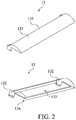
FIG. 2 is a structural schematic diagram illustrating the component protecting member of FIG. 1.
FIG. 3 is an assembly schematic diagram illustrating the circuit board and the component protecting member of FIG. 1.
FIG. 4 is a schematic diagram illustrating the circuit board and the component protecting member according to one embodiment of the present invention.
FIG. 5 is a schematic diagram illustrating the different shapes of the component protecting member according to another embodiment of the present invention.
FIG. 6A is a schematic diagram illustrating a high frequency connector according to another embodiment of the present invention.
FIG. 6B is a sectional diagram of the high frequency connector along the line A-A in FIG. 6A.
FIG. 7 is a schematic diagram illustrating the component protecting member according to another embodiment of the present invention.
FIG. 8 is an assembly schematic diagram illustrating the component protecting member and the circuit board of FIG. 7.
FIG. 9 is a flow diagram illustrating a method for manufacturing the high frequency connector according to one embodiment of the present invention.
FIG. 10 is a flow diagram illustrating the method for manufacturing the high frequency connector according to one embodiment of the present invention.
FIG. 11 is a flow diagram illustrating the method for manufacturing the high frequency connector according to one embodiment of the present invention.
FIG. 12 is a flow diagram illustrating the method for manufacturing the high frequency connector according to another embodiment of the present invention.
DETAILED DESCRIPTION OF THE INVENTION
For the sake of the advantages, spirits and features of the present invention can be understood more easily and clearly, the detailed descriptions and discussions will be made later by way of the embodiments and with reference of the diagrams. It is worth noting that these embodiments are merely representative embodiments of the present invention, wherein the specific methods, devices, conditions, materials and the like are not limited to the embodiments of the present invention or corresponding embodiments. Moreover, the devices in the figures are only used to express their corresponding positions and are not drawing according to their actual proportion.
Please refer to FIG. 1, FIG. 2, FIG. 3 and FIG. 4. FIG. 1 is an exploded diagram illustrating a high frequency connector 1 according to one embodiment of the present invention. FIG. 2 is a structural schematic diagram illustrating the component protecting member 13 of FIG. 1. FIG. 3 is an assembly schematic diagram illustrating the circuit board 12 and the component protecting member 13 of FIG. 1. FIG. 4 is a schematic diagram illustrating the circuit board 12 and the component protecting member 13 according to one embodiment of the present invention.
As shown in FIG. 1, the high frequency connector 1 of this embodiment includes a case 11, a circuit board 12, a component protecting member 13 and a cable 14. The circuit board 12 is configured in the case 11 and has a plurality of solder pads 127 and 128, an electronic component 122 and at least two positioning holes 124. The component protecting member 13 includes a case body 131 and at least two positioning pins 132 extended from the case body 131. The component protecting member 13 can be configured on the circuit board 12 by the positioning pins 132 inserting into the positioning holes 124 of the circuit board 12. One side of the case 11 includes an opening, and the circuit board 12 can be inserted and configured in the case 11 through the opening of the case 11.
As shown in FIG. 2, one side of the case body 131 of the component protecting member 13 has an opening 134. A containing space 133 is formed by the opening 134 and the inner surface of the case body 131, and a crossing structure 135 is disposed on the outer surface of the other side of the case body 131. The positioning pins 132 extend outward from the case body 131. In detail, the positioning pins 132 of this embodiment extend from the direction of the opening 134 of the case body 131. Moreover, the position and shape of the positioning pins 132 are corresponding to those of the positioning holes 124 of the circuit board 12, and the size of the positioning pins 132 can be slightly smaller than that of the positioning holes 124.
In practice, the component protecting member 13 is disposed on the circuit board 12 through the positioning pins 132 inserting into the positioning holes 124 of the circuit board 12. At this time, the bottom plane on the side of the opening 134 of the case body 131 of the component protecting member 13 attaches to the circuit board 12 so that the containing space 133 contains the electronic component 122 on the circuit board 12. That is to say, the component protecting member 13 covers the electronic component 122 on the circuit board 12. The electronic component 122 can be a high frequency transmitting or communicating electronic component. In this embodiment, the component protecting member 13 covers three electronic components 122, but it is not limited to three in practice. The number of the electronic component 122 can be 1, 2 or more than 3. Since the component protecting member 13 only needs to insert the positioning pins 132 into the positioning holes 124 of the circuit board 12 to be configured on the circuit board 12, the installation hours can be saved. It is worth to note that the positioning pins 132 of the component protecting member 13 in FIG. 2 are located on the same side and at the corners of the case body 131, but it is not limited thereto. In another embodiment, the positioning pins 132 of the component protecting member 13 can be located at the opposite corners or non-corner positions of the case body 131, which are corresponding to the positioning holes 124 of the circuit board 12. The shapes of the positioning pins 132 and the positioning holes 124 can be a circular shape or semi-circular shape (as shown in FIG. 2), also can be a polygon or corresponding shape. Moreover, the number of the positioning pins 132 is not limited to two in FIG. 1 and FIG. 2, the number of the positioning pin 132 configured on the case body 131 can be 1, 2 or more than 3. Similarly, the circuit board 12 has the positioning holes 124 with the corresponding positions and numbers to the positioning pins 132.
In general, the cable soldering positions of the connector are designed on the edge of the circuit board to prevent the cable from contacting the electronic component and affecting the transmission characteristic of the electronic component. As shown in FIG. 1, a first solder pad 127 is located on the edge of the circuit board 12. The first cable 141 can be soldered on the first solder pad 127 without contacting the electronic component when the conductive part 144 of the first cable 141 is soldered on the first solder pad 127. However, some of the cable soldering positions must be located on the non-edge positions of the circuit board under the situation of insufficient configuration space on the circuit board. As shown in FIG. 1 and FIG. 4, a second solder pad 128 is located among the electronic components 122 of the circuit board 12. Therefore, the insulating part 143 of the second cable 142 would contact the electronic component 122 when the conductive part 144 of the second cable 142 is soldered on the second solder pad 128. In practice, the medium covering on the electronic component 122 of the circuit board 12 affects the signal transmission characteristics, such as transmitting speed, signal integrity and so on. The optimum covering medium is air (the dielectric constant is 1, Dk=1). The dielectric constant of the electric component 122 is greater than 1 when the insulating part 143 of the second cable 142 contacts the electronic component 122. At this time, the transmission characteristic of the electronic component is affected, such as increasing the signal attenuation and reducing the transmission speed. Therefore, when the component protecting member 13 is configured on the circuit board 12, it can separate the electronic component 122 from the second cable to make the electronic component 122 not to contact the second cable 142 directly, and then maintain the transmission characteristic of the electronic component 122. In this embodiment, the second cable 142 is configured on the crossing structure 135 of the component protecting member 13 when the second cable 142 is soldered on the second solder pad 128, as shown in FIG. 4. Therefore, the component protecting member 143 blocks the second cable 142 by the case body 131 and protects the electronic component 122 through the containing space 133 to ensure the optimum dielectric medium around the electronic component 122, and then to maintain the transmission characteristic of the electronic component 122.
Moreover, in this embodiment, the maximum height of the containing space 133 of the component protecting member 13 is greater than that of the electronic component 122 of the circuit board 12. In practice, the component protecting member 13 not only blocks the second cable 142 from the electronic component 122, but also prevents the electronic component 122 from contacting the inner surface of the case body 131 of the component protecting member 13, so as to ensure the optimum dielectric medium around the electronic component 122 to maintain the signal transmission characteristics of the electronic component 122.
In the above embodiment, the component protecting member 13 is a curved sheet-like structure, but it is not limited thereto. Please refer to FIG. 5. FIG. 5 is a schematic diagram illustrating the different shapes of the component protecting members 13′, 13″, and 13′″ according to another one embodiment of the present invention. As shown in FIG. 5, the shapes of the crossing structures 135′, 135″, 135′″ of the component protecting members 13′, 13″, 13′″ can also be a polygon (such as a trapezoid or polygon with lead angle) or a combination of circular arc shape and polygon (such as a polygon with arc lead angle). In practice, any structure capable of forming a containing space and enabling the cable to be configured thereon can be adopted as the crossing structure of the component protecting member of the present invention. In another embodiment, the component protecting member 13 can include at least one rib configured at the inner surface of the case body to improve the structure strength of the component protecting member 13.
Please refer to FIG. 4, FIG. 6A and FIG. 6B. FIG. 6A is a schematic diagram illustrating a high frequency connector 1 according to another embodiment of the present invention. FIG. 6B is a sectional diagram of the high frequency connector 1 along the line A-A in FIG. 6A. As shown in FIG. 6A and FIG. 6B, the difference between the above embodiment and this embodiment is that a colloid 15 is used to adhere and fix the conductive parts 144 of the first cable 141 and the second cable 142 to the first solder pad 127 and the second solder pad 128 of the circuit board 12 respectively after soldering the first cable 141 and the second cable 142 on the circuit board 12. In this embodiment, the colloid 15 is further pasted on the insulating part 143 of the first cable 141 and the second cable 142 and the component protecting member 13. In practice, the colloid 15 fixes the first cable 141, the second cable 142 and the component protecting member 13 on the circuit board 12. It not only increases the holding strength of the first cable 141 and the second cable 142 and prevent the first cable 141 and the second cable 142 from being pulled off, but also prevents the component protecting member 13 from falling off. The component protecting member 13 can exclude the colloid 15 from the containing space 133 when the colloid 15 is pasted on the circuit board 12. Therefore, the electronic component 122 in the containing space 133 would not contact with the colloid 15, so as to maintain the signal transmission characteristics. In practice, the colloid 15 can be a waterproof glue or insulation glue. In another embodiment, the colloid 15 can be pasted on the circuit board 12, also can be pasted between the circuit board 12 and case 11 to make the structure of high frequency connector become more stable.
Please refer to FIG. 7 and FIG. 8. FIG. 7 is a schematic diagram illustrating the component protecting member 23 according to another one embodiment of the present invention. FIG. 8 is an assembly schematic diagram illustrating the component protecting member 23 and the circuit board 12 of FIG. 7. As shown in FIG. 7 and FIG. 8, the difference between the above embodiment and this embodiment is that the case body 231 of the component protecting member 23 includes at least one groove 236 configured on the outer surface of the crossing structure 235, so that the second cable 142 can be configured into each groove 236 when the component protecting member 23 is configured on the circuit board 12. In practice, the component protecting member 23 including the groove 236 not only makes the second cable 142 to be arranged neatly and less entangled, but also saves the space. Although the number of the grooves 236 of the component protecting member 23 is four in FIG. 7 and FIG. 8, but it is not limited thereto. The number of the grooves 236 can be 1, 2, 3 or more than 4 to match that of the second cable 142 configured on the component protecting member 23.
Please refer to FIG. 9. FIG. 9 is a flow diagram illustrating a method for manufacturing the high frequency connector according to one embodiment of the present invention. The present invention also provides a method for manufacturing the high frequency connector including the following steps of: step S1: soldering a conductive part of a first cable on a first solder pad of a circuit board; step S2: disposing a component protecting member on the circuit board to make the component protecting member to cover a electronic component of the circuit board; step S3: configuring a second cable across the component protecting member and soldering the second cable on a second solder pad of the circuit board; step S4: pasting a colloid on the first solder pad and the second solder pad of the circuit board; and step S5: disposing the circuit board, the component protecting member, the first cable and the second cable in a case. The method for manufacturing the high frequency connector shown in FIG. 9 can be achieved through the high frequency connector 1 shown in FIG. 1 and FIG. 4. The functions of the units mentioned in the steps of this embodiment are substantially the same as those of the corresponding units in the above embodiments, and thus will not be described herein. In practice, the sequence of step S1 and step S2 can be exchanged.
Please refer to FIG. 10. FIG. 10 is a flow diagram illustrating the method for manufacturing the high frequency connector according to one embodiment of the present invention. Step S2 further includes step S21: inserting at least two positioning pins of the component protecting member into at least two positioning holes of the circuit board correspondingly to make a containing space of the component protecting member to contain the electronic component.
Please refer to FIG. 11. FIG. 11 is a flow diagram illustrating the method for manufacturing the high frequency connector according to one embodiment of the present invention. Step S3 further includes step S31: configuring the insulating part of the second cable on the crossing structure of the component protecting member, and soldering the conductive part of the second cable on the second solder pad of the circuit board.
Please refer to FIG. 12. FIG. 12 is a flow diagram illustrating the method for manufacturing the high frequency connector according to another one embodiment of the present invention. Step S3 further includes step S32: configuring the second cable in at least one groove of the component protecting member and soldering the second cable on the second solder pad of the circuit board.
In conclusion, the high frequency connector of the present invention ensures that the electronic component contacts optimum dielectric medium to maintain the transmission characteristic of the electronic component by the component protecting member covering the electronic component on the circuit board.
With the examples and explanations mentioned above, the features and spirits of the invention are hopefully well described. More importantly, the present invention is not limited to the embodiment described herein. Those skilled in the art will readily observe that numerous modifications and alterations of the device may be made while retaining the teachings of the invention. Accordingly, the above disclosure should be construed as limited only by the metes and bounds of the appended claims.

Claims (8)

What is claimed is:
1. A high frequency connector, comprising:
a case;
a circuit board configured in the case, the circuit board having an electronic component and a plurality of solder pads disposed on the circuit board;
a component protecting member configured on the circuit board, the component protecting member comprising a case body, one side of the case body having an opening and a containing space being formed by the opening and an inner surface of the case body, a crossing structure being disposed on an outer surface of the other side of the case body, the crossing structure further comprising at least one groove, the electronic component being contained in the containing space; and
a cable configured in the groove, the cable comprising an insulating part and a conductive part disposed on the terminal of the cable, the insulating part of the cable being configured on the crossing structure, and the conductive part being soldered on the solder pads of the circuit board.
2. The high frequency connector of claim 1, wherein the circuit board further comprises at least one positioning hole, and the component protecting member comprises at least one positioning pin, the size of the at least one positioning pin is corresponding to that of the positioning hole.
3. The high frequency connector of claim 1, wherein the maximum height of the containing space is greater than that of the electronic component to prevent the electronic component from contacting the inner surface of the case body.
4. The high frequency connector of claim 1, wherein the shape of the crossing structure is one selected from the group consisting of a circular arc shape, a polygonal shape and a combination of both.
5. The high frequency connector of claim 1, further comprising a colloid pasted on the cable and the circuit board, the component protecting member blocking the colloid out of the containing space.
6. A method of manufacturing high frequency connector, comprising:
soldering a conductive part of a first cable on a first solder pad of a circuit board;
disposing a component protecting member on the circuit board to make the component protecting member to cover an electronic component of the circuit board, the component protecting member having at least one groove on the outer surface thereof;
configuring a second cable in the at least one groove and across the component protecting member and soldering the second cable on a second solder pad of the circuit board;
pasting a colloid on the first solder pad and the second solder pad of the circuit board; and
disposing the circuit board, the component protecting member, the first cable and the second cable in a case.
7. The method of claim 6, wherein the step of disposing the component protecting member on the circuit board to make the component protecting member to cover the electronic component of the circuit board further comprises the step of:
inserting at least one positioning pin of the component protecting member into at least one positioning hole of the circuit board correspondingly to make a containing space of the component protecting member to contain the electronic component.
8. The method of claim 6, wherein the step of configuring the second cable across the component protecting member and soldering the second cable on the second solder pad of the circuit board further comprises the step of:
configuring the insulating part of the second cable on the crossing structure of the component protecting member, and soldering the conductive part of the second cable on the second solder pad of the circuit board.
US16/677,466 2019-04-09 2019-11-07 High frequency connector with component protecting member and method of manufacturing thereof Active 2040-09-01 US11316303B2 (en)

Applications Claiming Priority (2)

Application Number Priority Date Filing Date Title
TW108112322A TWI735861B (en) 2019-04-09 2019-04-09 High frequency connector with component protecting member and method of manufacturing thereof
TW108112322 2019-04-09

Publications (2)

Publication Number Publication Date
US20200328561A1 US20200328561A1 (en) 2020-10-15
US11316303B2 true US11316303B2 (en) 2022-04-26

Family

ID=72749458

Family Applications (1)

Application Number Title Priority Date Filing Date
US16/677,466 Active 2040-09-01 US11316303B2 (en) 2019-04-09 2019-11-07 High frequency connector with component protecting member and method of manufacturing thereof

Country Status (2)

Country Link
US (1) US11316303B2 (en)
TW (1) TWI735861B (en)

Cited By (1)

* Cited by examiner, † Cited by third party
Publication number Priority date Publication date Assignee Title
US20230126311A1 (en) * 2021-10-25 2023-04-27 Jess-Link Products Co., Ltd. Cable connector with waterproof mechanism

Families Citing this family (2)

* Cited by examiner, † Cited by third party
Publication number Priority date Publication date Assignee Title
TWI735861B (en) * 2019-04-09 2021-08-11 佳必琪國際股份有限公司 High frequency connector with component protecting member and method of manufacturing thereof
US20230253748A1 (en) * 2022-02-08 2023-08-10 e-con Systems India Private Limited Method for Securing the Electrical Contacts in a Connector System

Citations (29)

* Cited by examiner, † Cited by third party
Publication number Priority date Publication date Assignee Title
US6053770A (en) * 1998-07-13 2000-04-25 The Whitaker Corporation Cable assembly adapted with a circuit board
US6203341B1 (en) * 1999-08-17 2001-03-20 Hon Hai Precision Ind. Co., Ltd. Cable connector
CN2466822Y (en) 2001-02-28 2001-12-19 宣得股份有限公司 Circuit board with electronic component connector
US6716057B1 (en) * 2002-10-03 2004-04-06 Hon Hai Precision Ind. Co., Ltd. Cable end connector assembly with improved shielding means
US7033202B2 (en) * 2003-03-12 2006-04-25 Hon Hai Precision Ind. Co., Ltd. Cable end connector having locking mechanism
US7118411B2 (en) * 2004-11-19 2006-10-10 Advanced Connectek Inc. System transformation connector
US7530844B2 (en) * 2006-12-22 2009-05-12 Hon Hai Precision Ind. Co., Ltd. Electrical connector with retaining member
US7563136B1 (en) * 2008-06-24 2009-07-21 Hon Hai Precision Ind. Co., Ltd. Cable assembly having interior shielding structure for suppressing electro-magnetic interference
US7578680B1 (en) * 2008-06-24 2009-08-25 Hon Hai Precision Ind. Co., Ltd. Cable assembly having interior shielding structure for suppressing electro-magnetic interference
US7758374B2 (en) * 2008-02-01 2010-07-20 Hon Hai Precision Ind. Co., Ltd. Cable connector assembly having wire management members with low profile
US20100315752A1 (en) * 2009-06-15 2010-12-16 Stanley Rabu Thermal protection circuits and structures for electronic devices and cables
CN102468561A (en) 2010-11-05 2012-05-23 富士康(昆山)电脑接插件有限公司 Cable connector assembly
US8303358B1 (en) * 2011-11-29 2012-11-06 Inventec Corporation Connector module and connector
US8562378B2 (en) * 2010-09-15 2013-10-22 Hon Hai Precision Industry Co., Ltd. Electrical connector assembly with an improved front cover
US8647149B2 (en) * 2009-10-22 2014-02-11 Sumitomo Electric Industries, Ltd. Connecting member-terminated multi-core coaxial cable and method for manufacture thereof
US20150288110A1 (en) * 2014-04-03 2015-10-08 Hosiden Corporation Connector
US20160006190A1 (en) * 2013-10-24 2016-01-07 Sanyo Electric Co., Ltd. Electrical cable and power supply device
US9431781B2 (en) * 2014-07-29 2016-08-30 BizConn International Corp. Signal connector for high-speed transmission
US20170110837A1 (en) * 2015-10-14 2017-04-20 Hosiden Corporation Plug connector and adapter
CN206758712U (en) 2017-03-27 2017-12-15 协讯电子(吉安)有限公司 The wire and cable connector of mobile terminal
US9847607B2 (en) * 2014-04-23 2017-12-19 Commscope Technologies Llc Electrical connector with shield cap and shielded terminals
US9979138B1 (en) * 2017-06-08 2018-05-22 Dongguan City Jianghan Electronics Co., Ltd USB function-type magnetic cable
US10096950B2 (en) * 2016-09-05 2018-10-09 Foxconn Interconnect Technology Limited Cable connector assembly having a physical resistor arranged in a larger one of two cable end connectors thereof
US10333249B1 (en) * 2018-08-02 2019-06-25 Shenzhen Tongyinhai Precision Electronics Co., Ltd Electronic connector with magnetic element and data transmission line using same
TWM584043U (en) 2019-04-09 2019-09-21 佳必琪國際股份有限公司 High frequency connector with component protecting member
US10574004B2 (en) * 2014-06-13 2020-02-25 Sony Corporaton Cable and power supply device
US20200328561A1 (en) * 2019-04-09 2020-10-15 Jess-Link Products Co., Ltd. High frequency connector with component protecting member and method of manufacturing thereof
US20210005350A1 (en) * 2018-07-13 2021-01-07 Lg Chem, Ltd. Data Cable Device Having Cable Battery
US10950962B2 (en) * 2017-11-21 2021-03-16 Lisa Draexlmaier Gmbh Electrical connector and electrical cable arrangement connected thereto

Patent Citations (29)

* Cited by examiner, † Cited by third party
Publication number Priority date Publication date Assignee Title
US6053770A (en) * 1998-07-13 2000-04-25 The Whitaker Corporation Cable assembly adapted with a circuit board
US6203341B1 (en) * 1999-08-17 2001-03-20 Hon Hai Precision Ind. Co., Ltd. Cable connector
CN2466822Y (en) 2001-02-28 2001-12-19 宣得股份有限公司 Circuit board with electronic component connector
US6716057B1 (en) * 2002-10-03 2004-04-06 Hon Hai Precision Ind. Co., Ltd. Cable end connector assembly with improved shielding means
US7033202B2 (en) * 2003-03-12 2006-04-25 Hon Hai Precision Ind. Co., Ltd. Cable end connector having locking mechanism
US7118411B2 (en) * 2004-11-19 2006-10-10 Advanced Connectek Inc. System transformation connector
US7530844B2 (en) * 2006-12-22 2009-05-12 Hon Hai Precision Ind. Co., Ltd. Electrical connector with retaining member
US7758374B2 (en) * 2008-02-01 2010-07-20 Hon Hai Precision Ind. Co., Ltd. Cable connector assembly having wire management members with low profile
US7563136B1 (en) * 2008-06-24 2009-07-21 Hon Hai Precision Ind. Co., Ltd. Cable assembly having interior shielding structure for suppressing electro-magnetic interference
US7578680B1 (en) * 2008-06-24 2009-08-25 Hon Hai Precision Ind. Co., Ltd. Cable assembly having interior shielding structure for suppressing electro-magnetic interference
US20100315752A1 (en) * 2009-06-15 2010-12-16 Stanley Rabu Thermal protection circuits and structures for electronic devices and cables
US8647149B2 (en) * 2009-10-22 2014-02-11 Sumitomo Electric Industries, Ltd. Connecting member-terminated multi-core coaxial cable and method for manufacture thereof
US8562378B2 (en) * 2010-09-15 2013-10-22 Hon Hai Precision Industry Co., Ltd. Electrical connector assembly with an improved front cover
CN102468561A (en) 2010-11-05 2012-05-23 富士康(昆山)电脑接插件有限公司 Cable connector assembly
US8303358B1 (en) * 2011-11-29 2012-11-06 Inventec Corporation Connector module and connector
US20160006190A1 (en) * 2013-10-24 2016-01-07 Sanyo Electric Co., Ltd. Electrical cable and power supply device
US20150288110A1 (en) * 2014-04-03 2015-10-08 Hosiden Corporation Connector
US9847607B2 (en) * 2014-04-23 2017-12-19 Commscope Technologies Llc Electrical connector with shield cap and shielded terminals
US10574004B2 (en) * 2014-06-13 2020-02-25 Sony Corporaton Cable and power supply device
US9431781B2 (en) * 2014-07-29 2016-08-30 BizConn International Corp. Signal connector for high-speed transmission
US20170110837A1 (en) * 2015-10-14 2017-04-20 Hosiden Corporation Plug connector and adapter
US10096950B2 (en) * 2016-09-05 2018-10-09 Foxconn Interconnect Technology Limited Cable connector assembly having a physical resistor arranged in a larger one of two cable end connectors thereof
CN206758712U (en) 2017-03-27 2017-12-15 协讯电子(吉安)有限公司 The wire and cable connector of mobile terminal
US9979138B1 (en) * 2017-06-08 2018-05-22 Dongguan City Jianghan Electronics Co., Ltd USB function-type magnetic cable
US10950962B2 (en) * 2017-11-21 2021-03-16 Lisa Draexlmaier Gmbh Electrical connector and electrical cable arrangement connected thereto
US20210005350A1 (en) * 2018-07-13 2021-01-07 Lg Chem, Ltd. Data Cable Device Having Cable Battery
US10333249B1 (en) * 2018-08-02 2019-06-25 Shenzhen Tongyinhai Precision Electronics Co., Ltd Electronic connector with magnetic element and data transmission line using same
TWM584043U (en) 2019-04-09 2019-09-21 佳必琪國際股份有限公司 High frequency connector with component protecting member
US20200328561A1 (en) * 2019-04-09 2020-10-15 Jess-Link Products Co., Ltd. High frequency connector with component protecting member and method of manufacturing thereof

Cited By (1)

* Cited by examiner, † Cited by third party
Publication number Priority date Publication date Assignee Title
US20230126311A1 (en) * 2021-10-25 2023-04-27 Jess-Link Products Co., Ltd. Cable connector with waterproof mechanism

Also Published As

Publication number Publication date
TW202038521A (en) 2020-10-16
TWI735861B (en) 2021-08-11
US20200328561A1 (en) 2020-10-15

Similar Documents

Publication Publication Date Title
KR102226482B1 (en) Connector with shield plate for shielding
US11316303B2 (en) High frequency connector with component protecting member and method of manufacturing thereof
US7214097B1 (en) Electrical connector with grounding effect
EP0444805B1 (en) Coaxial transmission line to strip line coupler
US11410790B2 (en) Substrate-mounted electrical connector for connecting to a shielded flat cable
US10827612B2 (en) Printed circuit board and electrical connector assembly using the same
JP6235164B2 (en) Cable termination
US11289854B2 (en) Electrical connecting device
US11277913B2 (en) Electrical connector assembly
US20170207549A1 (en) Data connector
US11469552B2 (en) Plug connector slidably inserted into receptacle connector
US20220384998A1 (en) Shielded flat cable and shielded flat cable with circuit board
US11862902B2 (en) Electrical connector with electromagnetic shielding function
JP5987721B2 (en) Cable connectors and cable assemblies
TWM584043U (en) High frequency connector with component protecting member
CN116686172A (en) Plug connector and connector assembly comprising a socket connector and a plug connector
CN209786274U (en) High frequency connector with element protection member
TW202145652A (en) Connector assembly including receptacle connector and plug connector
US20190319379A1 (en) High-rate signal connector module
KR101133630B1 (en) Receptacle connector improved in mounting structure
US11784438B2 (en) Connector attached multi-conductor cable
JP3620821B2 (en) Coaxial mixed flexible flat cable
KR20200010375A (en) Circuit module
CN113725642B (en) Connector assembly including receptacle connector and plug connector
TWI734514B (en) Compact connector for transmitting super high frequency signal

Legal Events

Date Code Title Description
FEPP Fee payment procedure

Free format text: ENTITY STATUS SET TO UNDISCOUNTED (ORIGINAL EVENT CODE: BIG.); ENTITY STATUS OF PATENT OWNER: LARGE ENTITY

AS Assignment

Owner name: JESS-LINK PRODUCTS CO., LTD., TAIWAN

Free format text: ASSIGNMENT OF ASSIGNORS INTEREST;ASSIGNOR:CHENG, CHIEH-MING;REEL/FRAME:050957/0284

Effective date: 20191107

STPP Information on status: patent application and granting procedure in general

Free format text: DOCKETED NEW CASE - READY FOR EXAMINATION

STPP Information on status: patent application and granting procedure in general

Free format text: NON FINAL ACTION MAILED

STPP Information on status: patent application and granting procedure in general

Free format text: NOTICE OF ALLOWANCE MAILED -- APPLICATION RECEIVED IN OFFICE OF PUBLICATIONS

STPP Information on status: patent application and granting procedure in general

Free format text: PUBLICATIONS -- ISSUE FEE PAYMENT VERIFIED

STCF Information on status: patent grant

Free format text: PATENTED CASE