US11264506B2 - Semiconductor device and manufacturing method thereof - Google Patents
Semiconductor device and manufacturing method thereof Download PDFInfo
- Publication number
- US11264506B2 US11264506B2 US16/658,768 US201916658768A US11264506B2 US 11264506 B2 US11264506 B2 US 11264506B2 US 201916658768 A US201916658768 A US 201916658768A US 11264506 B2 US11264506 B2 US 11264506B2
- Authority
- US
- United States
- Prior art keywords
- sacrificial
- layers
- forming
- semiconductor
- dielectric layer
- Prior art date
- Legal status (The legal status is an assumption and is not a legal conclusion. Google has not performed a legal analysis and makes no representation as to the accuracy of the status listed.)
- Active
Links
- 239000004065 semiconductor Substances 0.000 title claims abstract description 211
- 238000004519 manufacturing process Methods 0.000 title claims description 45
- 239000000463 material Substances 0.000 claims abstract description 53
- 238000000034 method Methods 0.000 claims description 69
- XLOMVQKBTHCTTD-UHFFFAOYSA-N Zinc monoxide Chemical compound [Zn]=O XLOMVQKBTHCTTD-UHFFFAOYSA-N 0.000 claims description 58
- 239000011787 zinc oxide Substances 0.000 claims description 29
- 229910052751 metal Inorganic materials 0.000 claims description 21
- 239000002184 metal Substances 0.000 claims description 21
- GYHNNYVSQQEPJS-UHFFFAOYSA-N Gallium Chemical compound [Ga] GYHNNYVSQQEPJS-UHFFFAOYSA-N 0.000 claims description 18
- 229910052733 gallium Inorganic materials 0.000 claims description 18
- 229910052738 indium Inorganic materials 0.000 claims description 18
- APFVFJFRJDLVQX-UHFFFAOYSA-N indium atom Chemical compound [In] APFVFJFRJDLVQX-UHFFFAOYSA-N 0.000 claims description 18
- 125000006850 spacer group Chemical group 0.000 claims description 18
- 229910052581 Si3N4 Inorganic materials 0.000 claims description 17
- HQVNEWCFYHHQES-UHFFFAOYSA-N silicon nitride Chemical compound N12[Si]34N5[Si]62N3[Si]51N64 HQVNEWCFYHHQES-UHFFFAOYSA-N 0.000 claims description 17
- 239000000758 substrate Substances 0.000 claims description 17
- 239000011810 insulating material Substances 0.000 claims description 15
- VYPSYNLAJGMNEJ-UHFFFAOYSA-N Silicium dioxide Chemical compound O=[Si]=O VYPSYNLAJGMNEJ-UHFFFAOYSA-N 0.000 claims description 13
- 239000013078 crystal Substances 0.000 claims description 13
- 229910052710 silicon Inorganic materials 0.000 claims description 13
- 229910052814 silicon oxide Inorganic materials 0.000 claims description 13
- 229910000577 Silicon-germanium Inorganic materials 0.000 claims description 12
- QZQVBEXLDFYHSR-UHFFFAOYSA-N gallium(III) oxide Inorganic materials O=[Ga]O[Ga]=O QZQVBEXLDFYHSR-UHFFFAOYSA-N 0.000 claims description 11
- PJXISJQVUVHSOJ-UHFFFAOYSA-N indium(III) oxide Inorganic materials [O-2].[O-2].[O-2].[In+3].[In+3] PJXISJQVUVHSOJ-UHFFFAOYSA-N 0.000 claims description 11
- ATJFFYVFTNAWJD-UHFFFAOYSA-N Tin Chemical compound [Sn] ATJFFYVFTNAWJD-UHFFFAOYSA-N 0.000 claims description 10
- 229910052718 tin Inorganic materials 0.000 claims description 10
- XUIMIQQOPSSXEZ-UHFFFAOYSA-N Silicon Chemical compound [Si] XUIMIQQOPSSXEZ-UHFFFAOYSA-N 0.000 claims description 9
- 239000010703 silicon Substances 0.000 claims description 9
- TWNQGVIAIRXVLR-UHFFFAOYSA-N oxo(oxoalumanyloxy)alumane Chemical compound O=[Al]O[Al]=O TWNQGVIAIRXVLR-UHFFFAOYSA-N 0.000 claims description 8
- 229910000449 hafnium oxide Inorganic materials 0.000 claims description 7
- WIHZLLGSGQNAGK-UHFFFAOYSA-N hafnium(4+);oxygen(2-) Chemical compound [O-2].[O-2].[Hf+4] WIHZLLGSGQNAGK-UHFFFAOYSA-N 0.000 claims description 7
- 229910021420 polycrystalline silicon Inorganic materials 0.000 claims description 6
- 150000004767 nitrides Chemical class 0.000 claims description 3
- 238000005498 polishing Methods 0.000 claims description 2
- 239000000126 substance Substances 0.000 claims description 2
- 229910004166 TaN Inorganic materials 0.000 claims 1
- 239000002135 nanosheet Substances 0.000 abstract description 47
- 239000010409 thin film Substances 0.000 abstract description 5
- 239000010410 layer Substances 0.000 description 278
- 230000008569 process Effects 0.000 description 38
- 238000000231 atomic layer deposition Methods 0.000 description 12
- 238000005229 chemical vapour deposition Methods 0.000 description 12
- 239000003989 dielectric material Substances 0.000 description 10
- 230000006870 function Effects 0.000 description 9
- 230000015572 biosynthetic process Effects 0.000 description 7
- 229910052782 aluminium Inorganic materials 0.000 description 6
- 239000010936 titanium Substances 0.000 description 6
- 230000008901 benefit Effects 0.000 description 5
- 239000004020 conductor Substances 0.000 description 5
- 238000005530 etching Methods 0.000 description 5
- 229910052732 germanium Inorganic materials 0.000 description 5
- 238000000059 patterning Methods 0.000 description 5
- 229910010038 TiAl Inorganic materials 0.000 description 4
- 229910017052 cobalt Inorganic materials 0.000 description 4
- 239000010941 cobalt Substances 0.000 description 4
- GUTLYIVDDKVIGB-UHFFFAOYSA-N cobalt atom Chemical compound [Co] GUTLYIVDDKVIGB-UHFFFAOYSA-N 0.000 description 4
- 229910052802 copper Inorganic materials 0.000 description 4
- 239000010949 copper Substances 0.000 description 4
- 238000000206 photolithography Methods 0.000 description 4
- 238000005240 physical vapour deposition Methods 0.000 description 4
- 239000011295 pitch Substances 0.000 description 4
- WGTYBPLFGIVFAS-UHFFFAOYSA-M tetramethylammonium hydroxide Chemical compound [OH-].C[N+](C)(C)C WGTYBPLFGIVFAS-UHFFFAOYSA-M 0.000 description 4
- 229910052719 titanium Inorganic materials 0.000 description 4
- 229910052721 tungsten Inorganic materials 0.000 description 4
- GWEVSGVZZGPLCZ-UHFFFAOYSA-N Titan oxide Chemical compound O=[Ti]=O GWEVSGVZZGPLCZ-UHFFFAOYSA-N 0.000 description 3
- 238000005520 cutting process Methods 0.000 description 3
- 239000010408 film Substances 0.000 description 3
- GNPVGFCGXDBREM-UHFFFAOYSA-N germanium atom Chemical compound [Ge] GNPVGFCGXDBREM-UHFFFAOYSA-N 0.000 description 3
- 239000011229 interlayer Substances 0.000 description 3
- 239000002356 single layer Substances 0.000 description 3
- 238000001039 wet etching Methods 0.000 description 3
- ITWBWJFEJCHKSN-UHFFFAOYSA-N 1,4,7-triazonane Chemical compound C1CNCCNCCN1 ITWBWJFEJCHKSN-UHFFFAOYSA-N 0.000 description 2
- RYGMFSIKBFXOCR-UHFFFAOYSA-N Copper Chemical compound [Cu] RYGMFSIKBFXOCR-UHFFFAOYSA-N 0.000 description 2
- 229910005542 GaSb Inorganic materials 0.000 description 2
- 229910001218 Gallium arsenide Inorganic materials 0.000 description 2
- 229910000530 Gallium indium arsenide Inorganic materials 0.000 description 2
- 229910004191 HfTi Inorganic materials 0.000 description 2
- -1 InAlAs Inorganic materials 0.000 description 2
- ZOKXTWBITQBERF-UHFFFAOYSA-N Molybdenum Chemical compound [Mo] ZOKXTWBITQBERF-UHFFFAOYSA-N 0.000 description 2
- 229910004200 TaSiN Inorganic materials 0.000 description 2
- 229910010041 TiAlC Inorganic materials 0.000 description 2
- 229910010037 TiAlN Inorganic materials 0.000 description 2
- 229910008484 TiSi Inorganic materials 0.000 description 2
- RTAQQCXQSZGOHL-UHFFFAOYSA-N Titanium Chemical compound [Ti] RTAQQCXQSZGOHL-UHFFFAOYSA-N 0.000 description 2
- MCMNRKCIXSYSNV-UHFFFAOYSA-N Zirconium dioxide Chemical compound O=[Zr]=O MCMNRKCIXSYSNV-UHFFFAOYSA-N 0.000 description 2
- XAGFODPZIPBFFR-UHFFFAOYSA-N aluminium Chemical compound [Al] XAGFODPZIPBFFR-UHFFFAOYSA-N 0.000 description 2
- PNEYBMLMFCGWSK-UHFFFAOYSA-N aluminium oxide Inorganic materials [O-2].[O-2].[O-2].[Al+3].[Al+3] PNEYBMLMFCGWSK-UHFFFAOYSA-N 0.000 description 2
- 229910021417 amorphous silicon Inorganic materials 0.000 description 2
- 230000004888 barrier function Effects 0.000 description 2
- 230000008859 change Effects 0.000 description 2
- 150000001875 compounds Chemical class 0.000 description 2
- 238000005137 deposition process Methods 0.000 description 2
- 238000010586 diagram Methods 0.000 description 2
- 238000001312 dry etching Methods 0.000 description 2
- 238000009713 electroplating Methods 0.000 description 2
- 238000005516 engineering process Methods 0.000 description 2
- 230000008020 evaporation Effects 0.000 description 2
- 238000001704 evaporation Methods 0.000 description 2
- 230000005669 field effect Effects 0.000 description 2
- CJNBYAVZURUTKZ-UHFFFAOYSA-N hafnium(IV) oxide Inorganic materials O=[Hf]=O CJNBYAVZURUTKZ-UHFFFAOYSA-N 0.000 description 2
- WPYVAWXEWQSOGY-UHFFFAOYSA-N indium antimonide Chemical compound [Sb]#[In] WPYVAWXEWQSOGY-UHFFFAOYSA-N 0.000 description 2
- 150000002500 ions Chemical class 0.000 description 2
- 238000004518 low pressure chemical vapour deposition Methods 0.000 description 2
- 229910052748 manganese Inorganic materials 0.000 description 2
- 229910001092 metal group alloy Inorganic materials 0.000 description 2
- 229910052750 molybdenum Inorganic materials 0.000 description 2
- 239000011733 molybdenum Substances 0.000 description 2
- 229910052759 nickel Inorganic materials 0.000 description 2
- PXHVJJICTQNCMI-UHFFFAOYSA-N nickel Substances [Ni] PXHVJJICTQNCMI-UHFFFAOYSA-N 0.000 description 2
- RUFLMLWJRZAWLJ-UHFFFAOYSA-N nickel silicide Chemical compound [Ni]=[Si]=[Ni] RUFLMLWJRZAWLJ-UHFFFAOYSA-N 0.000 description 2
- 229910021334 nickel silicide Inorganic materials 0.000 description 2
- 239000011368 organic material Substances 0.000 description 2
- 229910052763 palladium Inorganic materials 0.000 description 2
- 229910052697 platinum Inorganic materials 0.000 description 2
- 229920000642 polymer Polymers 0.000 description 2
- 229920005591 polysilicon Polymers 0.000 description 2
- 229910052702 rhenium Inorganic materials 0.000 description 2
- 229910021332 silicide Inorganic materials 0.000 description 2
- FVBUAEGBCNSCDD-UHFFFAOYSA-N silicide(4-) Chemical compound [Si-4] FVBUAEGBCNSCDD-UHFFFAOYSA-N 0.000 description 2
- 229910052709 silver Inorganic materials 0.000 description 2
- 239000010944 silver (metal) Substances 0.000 description 2
- 238000004544 sputter deposition Methods 0.000 description 2
- 229910003468 tantalcarbide Inorganic materials 0.000 description 2
- 229910052715 tantalum Inorganic materials 0.000 description 2
- GUVRBAGPIYLISA-UHFFFAOYSA-N tantalum atom Chemical compound [Ta] GUVRBAGPIYLISA-UHFFFAOYSA-N 0.000 description 2
- MZLGASXMSKOWSE-UHFFFAOYSA-N tantalum nitride Chemical compound [Ta]#N MZLGASXMSKOWSE-UHFFFAOYSA-N 0.000 description 2
- WFKWXMTUELFFGS-UHFFFAOYSA-N tungsten Chemical compound [W] WFKWXMTUELFFGS-UHFFFAOYSA-N 0.000 description 2
- 239000010937 tungsten Substances 0.000 description 2
- 229910052726 zirconium Inorganic materials 0.000 description 2
- 229910005898 GeSn Inorganic materials 0.000 description 1
- 229910004129 HfSiO Inorganic materials 0.000 description 1
- LEVVHYCKPQWKOP-UHFFFAOYSA-N [Si].[Ge] Chemical compound [Si].[Ge] LEVVHYCKPQWKOP-UHFFFAOYSA-N 0.000 description 1
- 229910045601 alloy Inorganic materials 0.000 description 1
- 239000000956 alloy Substances 0.000 description 1
- 230000004075 alteration Effects 0.000 description 1
- 238000000137 annealing Methods 0.000 description 1
- QVQLCTNNEUAWMS-UHFFFAOYSA-N barium oxide Inorganic materials [Ba]=O QVQLCTNNEUAWMS-UHFFFAOYSA-N 0.000 description 1
- ODINCKMPIJJUCX-UHFFFAOYSA-N calcium oxide Inorganic materials [Ca]=O ODINCKMPIJJUCX-UHFFFAOYSA-N 0.000 description 1
- 238000010276 construction Methods 0.000 description 1
- 229910052593 corundum Inorganic materials 0.000 description 1
- 229910021419 crystalline silicon Inorganic materials 0.000 description 1
- 238000000151 deposition Methods 0.000 description 1
- 230000009969 flowable effect Effects 0.000 description 1
- 229910052735 hafnium Inorganic materials 0.000 description 1
- VBJZVLUMGGDVMO-UHFFFAOYSA-N hafnium atom Chemical compound [Hf] VBJZVLUMGGDVMO-UHFFFAOYSA-N 0.000 description 1
- 229910000167 hafnon Inorganic materials 0.000 description 1
- 229910052741 iridium Inorganic materials 0.000 description 1
- MRELNEQAGSRDBK-UHFFFAOYSA-N lanthanum oxide Inorganic materials [O-2].[O-2].[O-2].[La+3].[La+3] MRELNEQAGSRDBK-UHFFFAOYSA-N 0.000 description 1
- 238000001459 lithography Methods 0.000 description 1
- CPLXHLVBOLITMK-UHFFFAOYSA-N magnesium oxide Inorganic materials [Mg]=O CPLXHLVBOLITMK-UHFFFAOYSA-N 0.000 description 1
- 230000015654 memory Effects 0.000 description 1
- 239000007769 metal material Substances 0.000 description 1
- 150000002739 metals Chemical class 0.000 description 1
- KTUFCUMIWABKDW-UHFFFAOYSA-N oxo(oxolanthaniooxy)lanthanum Chemical compound O=[La]O[La]=O KTUFCUMIWABKDW-UHFFFAOYSA-N 0.000 description 1
- RVTZCBVAJQQJTK-UHFFFAOYSA-N oxygen(2-);zirconium(4+) Chemical compound [O-2].[O-2].[Zr+4] RVTZCBVAJQQJTK-UHFFFAOYSA-N 0.000 description 1
- 238000002161 passivation Methods 0.000 description 1
- 230000000737 periodic effect Effects 0.000 description 1
- 238000005268 plasma chemical vapour deposition Methods 0.000 description 1
- 229910052707 ruthenium Inorganic materials 0.000 description 1
- 239000005368 silicate glass Substances 0.000 description 1
- 230000003068 static effect Effects 0.000 description 1
- IATRAKWUXMZMIY-UHFFFAOYSA-N strontium oxide Inorganic materials [O-2].[Sr+2] IATRAKWUXMZMIY-UHFFFAOYSA-N 0.000 description 1
- 238000006467 substitution reaction Methods 0.000 description 1
- PBCFLUZVCVVTBY-UHFFFAOYSA-N tantalum pentoxide Inorganic materials O=[Ta](=O)O[Ta](=O)=O PBCFLUZVCVVTBY-UHFFFAOYSA-N 0.000 description 1
- OGIDPMRJRNCKJF-UHFFFAOYSA-N titanium oxide Inorganic materials [Ti]=O OGIDPMRJRNCKJF-UHFFFAOYSA-N 0.000 description 1
- 229910001845 yogo sapphire Inorganic materials 0.000 description 1
- RUDFQVOCFDJEEF-UHFFFAOYSA-N yttrium(III) oxide Inorganic materials [O-2].[O-2].[O-2].[Y+3].[Y+3] RUDFQVOCFDJEEF-UHFFFAOYSA-N 0.000 description 1
- 229910052845 zircon Inorganic materials 0.000 description 1
- 229910001928 zirconium oxide Inorganic materials 0.000 description 1
Images


Classifications
-
- H—ELECTRICITY
- H01—ELECTRIC ELEMENTS
- H01L—SEMICONDUCTOR DEVICES NOT COVERED BY CLASS H10
- H01L29/00—Semiconductor devices specially adapted for rectifying, amplifying, oscillating or switching and having potential barriers; Capacitors or resistors having potential barriers, e.g. a PN-junction depletion layer or carrier concentration layer; Details of semiconductor bodies or of electrodes thereof ; Multistep manufacturing processes therefor
- H01L29/66—Types of semiconductor device ; Multistep manufacturing processes therefor
- H01L29/68—Types of semiconductor device ; Multistep manufacturing processes therefor controllable by only the electric current supplied, or only the electric potential applied, to an electrode which does not carry the current to be rectified, amplified or switched
- H01L29/76—Unipolar devices, e.g. field effect transistors
- H01L29/772—Field effect transistors
- H01L29/78—Field effect transistors with field effect produced by an insulated gate
- H01L29/786—Thin film transistors, i.e. transistors with a channel being at least partly a thin film
- H01L29/78696—Thin film transistors, i.e. transistors with a channel being at least partly a thin film characterised by the structure of the channel, e.g. multichannel, transverse or longitudinal shape, length or width, doping structure, or the overlap or alignment between the channel and the gate, the source or the drain, or the contacting structure of the channel
-
- B—PERFORMING OPERATIONS; TRANSPORTING
- B82—NANOTECHNOLOGY
- B82Y—SPECIFIC USES OR APPLICATIONS OF NANOSTRUCTURES; MEASUREMENT OR ANALYSIS OF NANOSTRUCTURES; MANUFACTURE OR TREATMENT OF NANOSTRUCTURES
- B82Y10/00—Nanotechnology for information processing, storage or transmission, e.g. quantum computing or single electron logic
-
- H—ELECTRICITY
- H01—ELECTRIC ELEMENTS
- H01L—SEMICONDUCTOR DEVICES NOT COVERED BY CLASS H10
- H01L27/00—Devices consisting of a plurality of semiconductor or other solid-state components formed in or on a common substrate
- H01L27/02—Devices consisting of a plurality of semiconductor or other solid-state components formed in or on a common substrate including semiconductor components specially adapted for rectifying, oscillating, amplifying or switching and having potential barriers; including integrated passive circuit elements having potential barriers
- H01L27/04—Devices consisting of a plurality of semiconductor or other solid-state components formed in or on a common substrate including semiconductor components specially adapted for rectifying, oscillating, amplifying or switching and having potential barriers; including integrated passive circuit elements having potential barriers the substrate being a semiconductor body
- H01L27/08—Devices consisting of a plurality of semiconductor or other solid-state components formed in or on a common substrate including semiconductor components specially adapted for rectifying, oscillating, amplifying or switching and having potential barriers; including integrated passive circuit elements having potential barriers the substrate being a semiconductor body including only semiconductor components of a single kind
- H01L27/085—Devices consisting of a plurality of semiconductor or other solid-state components formed in or on a common substrate including semiconductor components specially adapted for rectifying, oscillating, amplifying or switching and having potential barriers; including integrated passive circuit elements having potential barriers the substrate being a semiconductor body including only semiconductor components of a single kind including field-effect components only
- H01L27/088—Devices consisting of a plurality of semiconductor or other solid-state components formed in or on a common substrate including semiconductor components specially adapted for rectifying, oscillating, amplifying or switching and having potential barriers; including integrated passive circuit elements having potential barriers the substrate being a semiconductor body including only semiconductor components of a single kind including field-effect components only the components being field-effect transistors with insulated gate
- H01L27/0886—Devices consisting of a plurality of semiconductor or other solid-state components formed in or on a common substrate including semiconductor components specially adapted for rectifying, oscillating, amplifying or switching and having potential barriers; including integrated passive circuit elements having potential barriers the substrate being a semiconductor body including only semiconductor components of a single kind including field-effect components only the components being field-effect transistors with insulated gate including transistors with a horizontal current flow in a vertical sidewall of a semiconductor body, e.g. FinFET, MuGFET
-
- H—ELECTRICITY
- H01—ELECTRIC ELEMENTS
- H01L—SEMICONDUCTOR DEVICES NOT COVERED BY CLASS H10
- H01L21/00—Processes or apparatus adapted for the manufacture or treatment of semiconductor or solid state devices or of parts thereof
- H01L21/02—Manufacture or treatment of semiconductor devices or of parts thereof
- H01L21/02104—Forming layers
- H01L21/02107—Forming insulating materials on a substrate
- H01L21/02225—Forming insulating materials on a substrate characterised by the process for the formation of the insulating layer
- H01L21/0226—Forming insulating materials on a substrate characterised by the process for the formation of the insulating layer formation by a deposition process
- H01L21/02263—Forming insulating materials on a substrate characterised by the process for the formation of the insulating layer formation by a deposition process deposition from the gas or vapour phase
-
- H—ELECTRICITY
- H01—ELECTRIC ELEMENTS
- H01L—SEMICONDUCTOR DEVICES NOT COVERED BY CLASS H10
- H01L21/00—Processes or apparatus adapted for the manufacture or treatment of semiconductor or solid state devices or of parts thereof
- H01L21/70—Manufacture or treatment of devices consisting of a plurality of solid state components formed in or on a common substrate or of parts thereof; Manufacture of integrated circuit devices or of parts thereof
- H01L21/77—Manufacture or treatment of devices consisting of a plurality of solid state components or integrated circuits formed in, or on, a common substrate
- H01L21/78—Manufacture or treatment of devices consisting of a plurality of solid state components or integrated circuits formed in, or on, a common substrate with subsequent division of the substrate into plural individual devices
- H01L21/82—Manufacture or treatment of devices consisting of a plurality of solid state components or integrated circuits formed in, or on, a common substrate with subsequent division of the substrate into plural individual devices to produce devices, e.g. integrated circuits, each consisting of a plurality of components
- H01L21/822—Manufacture or treatment of devices consisting of a plurality of solid state components or integrated circuits formed in, or on, a common substrate with subsequent division of the substrate into plural individual devices to produce devices, e.g. integrated circuits, each consisting of a plurality of components the substrate being a semiconductor, using silicon technology
- H01L21/8232—Field-effect technology
- H01L21/8234—MIS technology, i.e. integration processes of field effect transistors of the conductor-insulator-semiconductor type
- H01L21/823431—MIS technology, i.e. integration processes of field effect transistors of the conductor-insulator-semiconductor type with a particular manufacturing method of transistors with a horizontal current flow in a vertical sidewall of a semiconductor body, e.g. FinFET, MuGFET
-
- H—ELECTRICITY
- H01—ELECTRIC ELEMENTS
- H01L—SEMICONDUCTOR DEVICES NOT COVERED BY CLASS H10
- H01L21/00—Processes or apparatus adapted for the manufacture or treatment of semiconductor or solid state devices or of parts thereof
- H01L21/70—Manufacture or treatment of devices consisting of a plurality of solid state components formed in or on a common substrate or of parts thereof; Manufacture of integrated circuit devices or of parts thereof
- H01L21/77—Manufacture or treatment of devices consisting of a plurality of solid state components or integrated circuits formed in, or on, a common substrate
- H01L21/78—Manufacture or treatment of devices consisting of a plurality of solid state components or integrated circuits formed in, or on, a common substrate with subsequent division of the substrate into plural individual devices
- H01L21/82—Manufacture or treatment of devices consisting of a plurality of solid state components or integrated circuits formed in, or on, a common substrate with subsequent division of the substrate into plural individual devices to produce devices, e.g. integrated circuits, each consisting of a plurality of components
- H01L21/822—Manufacture or treatment of devices consisting of a plurality of solid state components or integrated circuits formed in, or on, a common substrate with subsequent division of the substrate into plural individual devices to produce devices, e.g. integrated circuits, each consisting of a plurality of components the substrate being a semiconductor, using silicon technology
- H01L21/8232—Field-effect technology
- H01L21/8234—MIS technology, i.e. integration processes of field effect transistors of the conductor-insulator-semiconductor type
- H01L21/823468—MIS technology, i.e. integration processes of field effect transistors of the conductor-insulator-semiconductor type with a particular manufacturing method of the gate sidewall spacers, e.g. double spacers, particular spacer material or shape
-
- H—ELECTRICITY
- H01—ELECTRIC ELEMENTS
- H01L—SEMICONDUCTOR DEVICES NOT COVERED BY CLASS H10
- H01L27/00—Devices consisting of a plurality of semiconductor or other solid-state components formed in or on a common substrate
- H01L27/02—Devices consisting of a plurality of semiconductor or other solid-state components formed in or on a common substrate including semiconductor components specially adapted for rectifying, oscillating, amplifying or switching and having potential barriers; including integrated passive circuit elements having potential barriers
- H01L27/04—Devices consisting of a plurality of semiconductor or other solid-state components formed in or on a common substrate including semiconductor components specially adapted for rectifying, oscillating, amplifying or switching and having potential barriers; including integrated passive circuit elements having potential barriers the substrate being a semiconductor body
- H01L27/06—Devices consisting of a plurality of semiconductor or other solid-state components formed in or on a common substrate including semiconductor components specially adapted for rectifying, oscillating, amplifying or switching and having potential barriers; including integrated passive circuit elements having potential barriers the substrate being a semiconductor body including a plurality of individual components in a non-repetitive configuration
- H01L27/0688—Integrated circuits having a three-dimensional layout
-
- H—ELECTRICITY
- H01—ELECTRIC ELEMENTS
- H01L—SEMICONDUCTOR DEVICES NOT COVERED BY CLASS H10
- H01L27/00—Devices consisting of a plurality of semiconductor or other solid-state components formed in or on a common substrate
- H01L27/02—Devices consisting of a plurality of semiconductor or other solid-state components formed in or on a common substrate including semiconductor components specially adapted for rectifying, oscillating, amplifying or switching and having potential barriers; including integrated passive circuit elements having potential barriers
- H01L27/12—Devices consisting of a plurality of semiconductor or other solid-state components formed in or on a common substrate including semiconductor components specially adapted for rectifying, oscillating, amplifying or switching and having potential barriers; including integrated passive circuit elements having potential barriers the substrate being other than a semiconductor body, e.g. an insulating body
- H01L27/1203—Devices consisting of a plurality of semiconductor or other solid-state components formed in or on a common substrate including semiconductor components specially adapted for rectifying, oscillating, amplifying or switching and having potential barriers; including integrated passive circuit elements having potential barriers the substrate being other than a semiconductor body, e.g. an insulating body the substrate comprising an insulating body on a semiconductor body, e.g. SOI
- H01L27/1211—Devices consisting of a plurality of semiconductor or other solid-state components formed in or on a common substrate including semiconductor components specially adapted for rectifying, oscillating, amplifying or switching and having potential barriers; including integrated passive circuit elements having potential barriers the substrate being other than a semiconductor body, e.g. an insulating body the substrate comprising an insulating body on a semiconductor body, e.g. SOI combined with field-effect transistors with a horizontal current flow in a vertical sidewall of a semiconductor body, e.g. FinFET, MuGFET
-
- H—ELECTRICITY
- H01—ELECTRIC ELEMENTS
- H01L—SEMICONDUCTOR DEVICES NOT COVERED BY CLASS H10
- H01L27/00—Devices consisting of a plurality of semiconductor or other solid-state components formed in or on a common substrate
- H01L27/02—Devices consisting of a plurality of semiconductor or other solid-state components formed in or on a common substrate including semiconductor components specially adapted for rectifying, oscillating, amplifying or switching and having potential barriers; including integrated passive circuit elements having potential barriers
- H01L27/12—Devices consisting of a plurality of semiconductor or other solid-state components formed in or on a common substrate including semiconductor components specially adapted for rectifying, oscillating, amplifying or switching and having potential barriers; including integrated passive circuit elements having potential barriers the substrate being other than a semiconductor body, e.g. an insulating body
- H01L27/1214—Devices consisting of a plurality of semiconductor or other solid-state components formed in or on a common substrate including semiconductor components specially adapted for rectifying, oscillating, amplifying or switching and having potential barriers; including integrated passive circuit elements having potential barriers the substrate being other than a semiconductor body, e.g. an insulating body comprising a plurality of TFTs formed on a non-semiconducting substrate, e.g. driving circuits for AMLCDs
- H01L27/1222—Devices consisting of a plurality of semiconductor or other solid-state components formed in or on a common substrate including semiconductor components specially adapted for rectifying, oscillating, amplifying or switching and having potential barriers; including integrated passive circuit elements having potential barriers the substrate being other than a semiconductor body, e.g. an insulating body comprising a plurality of TFTs formed on a non-semiconducting substrate, e.g. driving circuits for AMLCDs with a particular composition, shape or crystalline structure of the active layer
- H01L27/1225—Devices consisting of a plurality of semiconductor or other solid-state components formed in or on a common substrate including semiconductor components specially adapted for rectifying, oscillating, amplifying or switching and having potential barriers; including integrated passive circuit elements having potential barriers the substrate being other than a semiconductor body, e.g. an insulating body comprising a plurality of TFTs formed on a non-semiconducting substrate, e.g. driving circuits for AMLCDs with a particular composition, shape or crystalline structure of the active layer with semiconductor materials not belonging to the group IV of the periodic table, e.g. InGaZnO
-
- H—ELECTRICITY
- H01—ELECTRIC ELEMENTS
- H01L—SEMICONDUCTOR DEVICES NOT COVERED BY CLASS H10
- H01L27/00—Devices consisting of a plurality of semiconductor or other solid-state components formed in or on a common substrate
- H01L27/02—Devices consisting of a plurality of semiconductor or other solid-state components formed in or on a common substrate including semiconductor components specially adapted for rectifying, oscillating, amplifying or switching and having potential barriers; including integrated passive circuit elements having potential barriers
- H01L27/12—Devices consisting of a plurality of semiconductor or other solid-state components formed in or on a common substrate including semiconductor components specially adapted for rectifying, oscillating, amplifying or switching and having potential barriers; including integrated passive circuit elements having potential barriers the substrate being other than a semiconductor body, e.g. an insulating body
- H01L27/1214—Devices consisting of a plurality of semiconductor or other solid-state components formed in or on a common substrate including semiconductor components specially adapted for rectifying, oscillating, amplifying or switching and having potential barriers; including integrated passive circuit elements having potential barriers the substrate being other than a semiconductor body, e.g. an insulating body comprising a plurality of TFTs formed on a non-semiconducting substrate, e.g. driving circuits for AMLCDs
- H01L27/1259—Multistep manufacturing methods
- H01L27/1288—Multistep manufacturing methods employing particular masking sequences or specially adapted masks, e.g. half-tone mask
-
- H—ELECTRICITY
- H01—ELECTRIC ELEMENTS
- H01L—SEMICONDUCTOR DEVICES NOT COVERED BY CLASS H10
- H01L29/00—Semiconductor devices specially adapted for rectifying, amplifying, oscillating or switching and having potential barriers; Capacitors or resistors having potential barriers, e.g. a PN-junction depletion layer or carrier concentration layer; Details of semiconductor bodies or of electrodes thereof ; Multistep manufacturing processes therefor
- H01L29/02—Semiconductor bodies ; Multistep manufacturing processes therefor
- H01L29/04—Semiconductor bodies ; Multistep manufacturing processes therefor characterised by their crystalline structure, e.g. polycrystalline, cubic or particular orientation of crystalline planes
- H01L29/045—Semiconductor bodies ; Multistep manufacturing processes therefor characterised by their crystalline structure, e.g. polycrystalline, cubic or particular orientation of crystalline planes by their particular orientation of crystalline planes
-
- H—ELECTRICITY
- H01—ELECTRIC ELEMENTS
- H01L—SEMICONDUCTOR DEVICES NOT COVERED BY CLASS H10
- H01L29/00—Semiconductor devices specially adapted for rectifying, amplifying, oscillating or switching and having potential barriers; Capacitors or resistors having potential barriers, e.g. a PN-junction depletion layer or carrier concentration layer; Details of semiconductor bodies or of electrodes thereof ; Multistep manufacturing processes therefor
- H01L29/02—Semiconductor bodies ; Multistep manufacturing processes therefor
- H01L29/06—Semiconductor bodies ; Multistep manufacturing processes therefor characterised by their shape; characterised by the shapes, relative sizes, or dispositions of the semiconductor regions ; characterised by the concentration or distribution of impurities within semiconductor regions
- H01L29/0657—Semiconductor bodies ; Multistep manufacturing processes therefor characterised by their shape; characterised by the shapes, relative sizes, or dispositions of the semiconductor regions ; characterised by the concentration or distribution of impurities within semiconductor regions characterised by the shape of the body
- H01L29/0665—Semiconductor bodies ; Multistep manufacturing processes therefor characterised by their shape; characterised by the shapes, relative sizes, or dispositions of the semiconductor regions ; characterised by the concentration or distribution of impurities within semiconductor regions characterised by the shape of the body the shape of the body defining a nanostructure
- H01L29/0669—Nanowires or nanotubes
- H01L29/0673—Nanowires or nanotubes oriented parallel to a substrate
-
- H—ELECTRICITY
- H01—ELECTRIC ELEMENTS
- H01L—SEMICONDUCTOR DEVICES NOT COVERED BY CLASS H10
- H01L29/00—Semiconductor devices specially adapted for rectifying, amplifying, oscillating or switching and having potential barriers; Capacitors or resistors having potential barriers, e.g. a PN-junction depletion layer or carrier concentration layer; Details of semiconductor bodies or of electrodes thereof ; Multistep manufacturing processes therefor
- H01L29/02—Semiconductor bodies ; Multistep manufacturing processes therefor
- H01L29/06—Semiconductor bodies ; Multistep manufacturing processes therefor characterised by their shape; characterised by the shapes, relative sizes, or dispositions of the semiconductor regions ; characterised by the concentration or distribution of impurities within semiconductor regions
- H01L29/08—Semiconductor bodies ; Multistep manufacturing processes therefor characterised by their shape; characterised by the shapes, relative sizes, or dispositions of the semiconductor regions ; characterised by the concentration or distribution of impurities within semiconductor regions with semiconductor regions connected to an electrode carrying current to be rectified, amplified or switched and such electrode being part of a semiconductor device which comprises three or more electrodes
- H01L29/0843—Source or drain regions of field-effect devices
- H01L29/0847—Source or drain regions of field-effect devices of field-effect transistors with insulated gate
-
- H—ELECTRICITY
- H01—ELECTRIC ELEMENTS
- H01L—SEMICONDUCTOR DEVICES NOT COVERED BY CLASS H10
- H01L29/00—Semiconductor devices specially adapted for rectifying, amplifying, oscillating or switching and having potential barriers; Capacitors or resistors having potential barriers, e.g. a PN-junction depletion layer or carrier concentration layer; Details of semiconductor bodies or of electrodes thereof ; Multistep manufacturing processes therefor
- H01L29/02—Semiconductor bodies ; Multistep manufacturing processes therefor
- H01L29/06—Semiconductor bodies ; Multistep manufacturing processes therefor characterised by their shape; characterised by the shapes, relative sizes, or dispositions of the semiconductor regions ; characterised by the concentration or distribution of impurities within semiconductor regions
- H01L29/10—Semiconductor bodies ; Multistep manufacturing processes therefor characterised by their shape; characterised by the shapes, relative sizes, or dispositions of the semiconductor regions ; characterised by the concentration or distribution of impurities within semiconductor regions with semiconductor regions connected to an electrode not carrying current to be rectified, amplified or switched and such electrode being part of a semiconductor device which comprises three or more electrodes
- H01L29/107—Substrate region of field-effect devices
- H01L29/1075—Substrate region of field-effect devices of field-effect transistors
- H01L29/1079—Substrate region of field-effect devices of field-effect transistors with insulated gate
-
- H—ELECTRICITY
- H01—ELECTRIC ELEMENTS
- H01L—SEMICONDUCTOR DEVICES NOT COVERED BY CLASS H10
- H01L29/00—Semiconductor devices specially adapted for rectifying, amplifying, oscillating or switching and having potential barriers; Capacitors or resistors having potential barriers, e.g. a PN-junction depletion layer or carrier concentration layer; Details of semiconductor bodies or of electrodes thereof ; Multistep manufacturing processes therefor
- H01L29/02—Semiconductor bodies ; Multistep manufacturing processes therefor
- H01L29/12—Semiconductor bodies ; Multistep manufacturing processes therefor characterised by the materials of which they are formed
- H01L29/24—Semiconductor bodies ; Multistep manufacturing processes therefor characterised by the materials of which they are formed including, apart from doping materials or other impurities, only semiconductor materials not provided for in groups H01L29/16, H01L29/18, H01L29/20, H01L29/22
- H01L29/247—Amorphous materials
-
- H—ELECTRICITY
- H01—ELECTRIC ELEMENTS
- H01L—SEMICONDUCTOR DEVICES NOT COVERED BY CLASS H10
- H01L29/00—Semiconductor devices specially adapted for rectifying, amplifying, oscillating or switching and having potential barriers; Capacitors or resistors having potential barriers, e.g. a PN-junction depletion layer or carrier concentration layer; Details of semiconductor bodies or of electrodes thereof ; Multistep manufacturing processes therefor
- H01L29/40—Electrodes ; Multistep manufacturing processes therefor
- H01L29/41—Electrodes ; Multistep manufacturing processes therefor characterised by their shape, relative sizes or dispositions
- H01L29/423—Electrodes ; Multistep manufacturing processes therefor characterised by their shape, relative sizes or dispositions not carrying the current to be rectified, amplified or switched
- H01L29/42312—Gate electrodes for field effect devices
- H01L29/42316—Gate electrodes for field effect devices for field-effect transistors
- H01L29/4232—Gate electrodes for field effect devices for field-effect transistors with insulated gate
- H01L29/42384—Gate electrodes for field effect devices for field-effect transistors with insulated gate for thin film field effect transistors, e.g. characterised by the thickness or the shape of the insulator or the dimensions, the shape or the lay-out of the conductor
- H01L29/42392—Gate electrodes for field effect devices for field-effect transistors with insulated gate for thin film field effect transistors, e.g. characterised by the thickness or the shape of the insulator or the dimensions, the shape or the lay-out of the conductor fully surrounding the channel, e.g. gate-all-around
-
- H—ELECTRICITY
- H01—ELECTRIC ELEMENTS
- H01L—SEMICONDUCTOR DEVICES NOT COVERED BY CLASS H10
- H01L29/00—Semiconductor devices specially adapted for rectifying, amplifying, oscillating or switching and having potential barriers; Capacitors or resistors having potential barriers, e.g. a PN-junction depletion layer or carrier concentration layer; Details of semiconductor bodies or of electrodes thereof ; Multistep manufacturing processes therefor
- H01L29/66—Types of semiconductor device ; Multistep manufacturing processes therefor
- H01L29/66007—Multistep manufacturing processes
- H01L29/66075—Multistep manufacturing processes of devices having semiconductor bodies comprising group 14 or group 13/15 materials
- H01L29/66227—Multistep manufacturing processes of devices having semiconductor bodies comprising group 14 or group 13/15 materials the devices being controllable only by the electric current supplied or the electric potential applied, to an electrode which does not carry the current to be rectified, amplified or switched, e.g. three-terminal devices
- H01L29/66409—Unipolar field-effect transistors
- H01L29/66439—Unipolar field-effect transistors with a one- or zero-dimensional channel, e.g. quantum wire FET, in-plane gate transistor [IPG], single electron transistor [SET], striped channel transistor, Coulomb blockade transistor
-
- H—ELECTRICITY
- H01—ELECTRIC ELEMENTS
- H01L—SEMICONDUCTOR DEVICES NOT COVERED BY CLASS H10
- H01L29/00—Semiconductor devices specially adapted for rectifying, amplifying, oscillating or switching and having potential barriers; Capacitors or resistors having potential barriers, e.g. a PN-junction depletion layer or carrier concentration layer; Details of semiconductor bodies or of electrodes thereof ; Multistep manufacturing processes therefor
- H01L29/66—Types of semiconductor device ; Multistep manufacturing processes therefor
- H01L29/66007—Multistep manufacturing processes
- H01L29/66075—Multistep manufacturing processes of devices having semiconductor bodies comprising group 14 or group 13/15 materials
- H01L29/66227—Multistep manufacturing processes of devices having semiconductor bodies comprising group 14 or group 13/15 materials the devices being controllable only by the electric current supplied or the electric potential applied, to an electrode which does not carry the current to be rectified, amplified or switched, e.g. three-terminal devices
- H01L29/66409—Unipolar field-effect transistors
- H01L29/66477—Unipolar field-effect transistors with an insulated gate, i.e. MISFET
- H01L29/66545—Unipolar field-effect transistors with an insulated gate, i.e. MISFET using a dummy, i.e. replacement gate in a process wherein at least a part of the final gate is self aligned to the dummy gate
-
- H—ELECTRICITY
- H01—ELECTRIC ELEMENTS
- H01L—SEMICONDUCTOR DEVICES NOT COVERED BY CLASS H10
- H01L29/00—Semiconductor devices specially adapted for rectifying, amplifying, oscillating or switching and having potential barriers; Capacitors or resistors having potential barriers, e.g. a PN-junction depletion layer or carrier concentration layer; Details of semiconductor bodies or of electrodes thereof ; Multistep manufacturing processes therefor
- H01L29/66—Types of semiconductor device ; Multistep manufacturing processes therefor
- H01L29/66007—Multistep manufacturing processes
- H01L29/66075—Multistep manufacturing processes of devices having semiconductor bodies comprising group 14 or group 13/15 materials
- H01L29/66227—Multistep manufacturing processes of devices having semiconductor bodies comprising group 14 or group 13/15 materials the devices being controllable only by the electric current supplied or the electric potential applied, to an electrode which does not carry the current to be rectified, amplified or switched, e.g. three-terminal devices
- H01L29/66409—Unipolar field-effect transistors
- H01L29/66477—Unipolar field-effect transistors with an insulated gate, i.e. MISFET
- H01L29/66742—Thin film unipolar transistors
-
- H—ELECTRICITY
- H01—ELECTRIC ELEMENTS
- H01L—SEMICONDUCTOR DEVICES NOT COVERED BY CLASS H10
- H01L29/00—Semiconductor devices specially adapted for rectifying, amplifying, oscillating or switching and having potential barriers; Capacitors or resistors having potential barriers, e.g. a PN-junction depletion layer or carrier concentration layer; Details of semiconductor bodies or of electrodes thereof ; Multistep manufacturing processes therefor
- H01L29/66—Types of semiconductor device ; Multistep manufacturing processes therefor
- H01L29/66007—Multistep manufacturing processes
- H01L29/66075—Multistep manufacturing processes of devices having semiconductor bodies comprising group 14 or group 13/15 materials
- H01L29/66227—Multistep manufacturing processes of devices having semiconductor bodies comprising group 14 or group 13/15 materials the devices being controllable only by the electric current supplied or the electric potential applied, to an electrode which does not carry the current to be rectified, amplified or switched, e.g. three-terminal devices
- H01L29/66409—Unipolar field-effect transistors
- H01L29/66477—Unipolar field-effect transistors with an insulated gate, i.e. MISFET
- H01L29/66787—Unipolar field-effect transistors with an insulated gate, i.e. MISFET with a gate at the side of the channel
- H01L29/66795—Unipolar field-effect transistors with an insulated gate, i.e. MISFET with a gate at the side of the channel with a horizontal current flow in a vertical sidewall of a semiconductor body, e.g. FinFET, MuGFET
-
- H—ELECTRICITY
- H01—ELECTRIC ELEMENTS
- H01L—SEMICONDUCTOR DEVICES NOT COVERED BY CLASS H10
- H01L29/00—Semiconductor devices specially adapted for rectifying, amplifying, oscillating or switching and having potential barriers; Capacitors or resistors having potential barriers, e.g. a PN-junction depletion layer or carrier concentration layer; Details of semiconductor bodies or of electrodes thereof ; Multistep manufacturing processes therefor
- H01L29/66—Types of semiconductor device ; Multistep manufacturing processes therefor
- H01L29/66007—Multistep manufacturing processes
- H01L29/66969—Multistep manufacturing processes of devices having semiconductor bodies not comprising group 14 or group 13/15 materials
-
- H—ELECTRICITY
- H01—ELECTRIC ELEMENTS
- H01L—SEMICONDUCTOR DEVICES NOT COVERED BY CLASS H10
- H01L29/00—Semiconductor devices specially adapted for rectifying, amplifying, oscillating or switching and having potential barriers; Capacitors or resistors having potential barriers, e.g. a PN-junction depletion layer or carrier concentration layer; Details of semiconductor bodies or of electrodes thereof ; Multistep manufacturing processes therefor
- H01L29/66—Types of semiconductor device ; Multistep manufacturing processes therefor
- H01L29/68—Types of semiconductor device ; Multistep manufacturing processes therefor controllable by only the electric current supplied, or only the electric potential applied, to an electrode which does not carry the current to be rectified, amplified or switched
- H01L29/76—Unipolar devices, e.g. field effect transistors
- H01L29/772—Field effect transistors
- H01L29/775—Field effect transistors with one dimensional charge carrier gas channel, e.g. quantum wire FET
-
- H—ELECTRICITY
- H01—ELECTRIC ELEMENTS
- H01L—SEMICONDUCTOR DEVICES NOT COVERED BY CLASS H10
- H01L29/00—Semiconductor devices specially adapted for rectifying, amplifying, oscillating or switching and having potential barriers; Capacitors or resistors having potential barriers, e.g. a PN-junction depletion layer or carrier concentration layer; Details of semiconductor bodies or of electrodes thereof ; Multistep manufacturing processes therefor
- H01L29/66—Types of semiconductor device ; Multistep manufacturing processes therefor
- H01L29/68—Types of semiconductor device ; Multistep manufacturing processes therefor controllable by only the electric current supplied, or only the electric potential applied, to an electrode which does not carry the current to be rectified, amplified or switched
- H01L29/76—Unipolar devices, e.g. field effect transistors
- H01L29/772—Field effect transistors
- H01L29/78—Field effect transistors with field effect produced by an insulated gate
- H01L29/785—Field effect transistors with field effect produced by an insulated gate having a channel with a horizontal current flow in a vertical sidewall of a semiconductor body, e.g. FinFET, MuGFET
- H01L29/7853—Field effect transistors with field effect produced by an insulated gate having a channel with a horizontal current flow in a vertical sidewall of a semiconductor body, e.g. FinFET, MuGFET the body having a non-rectangular crossection
-
- H—ELECTRICITY
- H01—ELECTRIC ELEMENTS
- H01L—SEMICONDUCTOR DEVICES NOT COVERED BY CLASS H10
- H01L29/00—Semiconductor devices specially adapted for rectifying, amplifying, oscillating or switching and having potential barriers; Capacitors or resistors having potential barriers, e.g. a PN-junction depletion layer or carrier concentration layer; Details of semiconductor bodies or of electrodes thereof ; Multistep manufacturing processes therefor
- H01L29/66—Types of semiconductor device ; Multistep manufacturing processes therefor
- H01L29/68—Types of semiconductor device ; Multistep manufacturing processes therefor controllable by only the electric current supplied, or only the electric potential applied, to an electrode which does not carry the current to be rectified, amplified or switched
- H01L29/76—Unipolar devices, e.g. field effect transistors
- H01L29/772—Field effect transistors
- H01L29/78—Field effect transistors with field effect produced by an insulated gate
- H01L29/786—Thin film transistors, i.e. transistors with a channel being at least partly a thin film
- H01L29/7869—Thin film transistors, i.e. transistors with a channel being at least partly a thin film having a semiconductor body comprising an oxide semiconductor material, e.g. zinc oxide, copper aluminium oxide, cadmium stannate
- H01L29/78693—Thin film transistors, i.e. transistors with a channel being at least partly a thin film having a semiconductor body comprising an oxide semiconductor material, e.g. zinc oxide, copper aluminium oxide, cadmium stannate the semiconducting oxide being amorphous
Definitions
- the cell height is generally defined as a periodic distance (pitch) between two power supply lines, VDD and VSS, and is generally determined by the number and a pitch of fin structures and/or metal lines.
- the cell height is also called a track height. Typical track heights are 7.5 T, 6.5 T or 5.5 T, where T is a smallest pitch of metal lines running over the standard cell. Scaling down to 4.5 T or 4 T is currently required to further minimize the size of semiconductor devices.
- FIG. 1 shows a circuit diagram of a semiconductor device according to an embodiment of the present disclosure.
- FIG. 2 shows a cross sectional view of a semiconductor device according to an embodiment of the present disclosure.
- FIG. 3 shows a cross sectional view of a semiconductor device according to an embodiment of the present disclosure.
- FIG. 4 shows a cross sectional view of a semiconductor device according to an embodiment of the present disclosure.
- FIG. 5 shows a cross sectional view of a semiconductor device according to an embodiment of the present disclosure.
- FIGS. 6A and 6B are schematic illustrations of a sequential process of manufacturing a semiconductor device according to an embodiment of the present disclosure.
- FIG. 6A is an isometric view and
- FIG. 6B is a plan view.
- FIGS. 7A and 7B are schematic illustrations of a sequential process of manufacturing a semiconductor device according to an embodiment of the present disclosure.
- FIG. 7A is an isometric view and
- FIG. 7B is a plan view.
- FIGS. 8A and 8B are schematic illustrations of a sequential process of manufacturing a semiconductor device according to an embodiment of the present disclosure.
- FIG. 8A is an isometric view and
- FIG. 8B is a plan view.
- FIGS. 9A and 9B are schematic illustrations of a sequential process of manufacturing a semiconductor device according to an embodiment of the present disclosure.
- FIG. 9A is an isometric view and
- FIG. 9B is a plan view.
- FIGS. 10A and 10B are schematic illustrations of a sequential process of manufacturing a semiconductor device according to an embodiment of the present disclosure.
- FIG. 10A is an isometric view and
- FIG. 10B is a plan view.
- FIGS. 11A and 11B are schematic illustrations of a sequential process of manufacturing a semiconductor device according to an embodiment of the present disclosure.
- FIG. 11A is an isometric view and
- FIG. 11B is a plan view.
- FIGS. 12A and 12B are schematic illustrations of a sequential process of manufacturing a semiconductor device according to an embodiment of the present disclosure.
- FIG. 12A is an isometric view and
- FIG. 12B is a plan view.
- FIGS. 13A and 13B are schematic illustrations of a sequential process of manufacturing a semiconductor device according to an embodiment of the present disclosure.
- FIG. 13A is an isometric view and
- FIG. 13B is a plan view.
- FIGS. 14A and 14B are schematic illustrations of a sequential process of manufacturing a semiconductor device according to an embodiment of the present disclosure.
- FIG. 14A is an isometric view and
- FIG. 14B is a plan view.
- FIGS. 15A and 15B are schematic illustrations of a sequential process of manufacturing a semiconductor device according to an embodiment of the present disclosure.
- FIG. 15A is an isometric view and
- FIG. 15B is a plan view.
- FIGS. 16A and 16B are schematic illustrations of a sequential process of manufacturing a semiconductor device according to an embodiment of the present disclosure.
- FIG. 16A is an isometric view and
- FIG. 16B is a plan view.
- FIGS. 17A and 17B are schematic illustrations of a sequential process of manufacturing a semiconductor device according to an embodiment of the present disclosure.
- FIG. 17A is an isometric view and
- FIG. 17B is a plan view.
- FIGS. 18A and 18B are schematic illustrations of a sequential process of manufacturing a semiconductor device according to an embodiment of the present disclosure.
- FIG. 18A is an isometric view and
- FIG. 18B is a plan view.
- FIGS. 19A and 19B are schematic illustrations of a sequential process of manufacturing a semiconductor device according to an embodiment of the present disclosure.
- FIG. 19A is an isometric view and
- FIG. 19B is a plan view.
- FIGS. 20A and 20B are schematic illustrations of a sequential process of manufacturing a semiconductor device according to an embodiment of the present disclosure.
- FIG. 20A is an isometric view and
- FIG. 20B is a plan view
- FIGS. 21A and 21B are schematic illustrations of a sequential process of manufacturing a semiconductor device according to an embodiment of the present disclosure.
- FIG. 21A is an isometric view and
- FIG. 21B is a plan view
- FIGS. 22A and 22B are schematic illustrations of a sequential process of manufacturing a semiconductor device according to an embodiment of the present disclosure.
- FIG. 22A is an isometric view and
- FIG. 22B is a plan view.
- FIG. 23 shows a cross sectional view of a semiconductor FET device according to an embodiment of the present disclosure.
- spatially relative terms such as “beneath,” “below,” “lower,” “above,” “upper” and the like, may be used herein for ease of description to describe one element or feature's relationship to another element(s) or feature(s) as illustrated in the figures.
- the spatially relative terms are intended to encompass different orientations of the device in use or operation in addition to the orientation depicted in the figures.
- the device may be otherwise oriented (rotated 90 degrees or at other orientations) and the spatially relative descriptors used herein may likewise be interpreted accordingly.
- the term “made of” may mean either “comprising” or “consisting of.” Further, in the following fabrication process, there may be one or more additional operations in/between the described operations, and the order of operations may be changed. In the following embodiments, the term “upper” “over” and/or “above” are defined along directions with an increase in a distance from the front surface and the back surface. Materials, configurations, dimensions, processes and/or operations as explained with respect to one embodiment may be employed in the other embodiments, and the detailed description thereon may be omitted.
- VVDD and/or VVSS virtual power supply line
- VDD and/or VSS main power supply line
- the virtual power supply line may be called a local power supply line, while the main power supply line may be called a global power supply line.
- VDD is generally at a higher potential (voltage) than VSS, and in some embodiments, VSS is coupled to the ground (0 V).
- the power consumption is reduced by turning-off (opening) the header/footer switch coupled to a non-active functional circuit in the semiconductor device.
- a first main power supply line VDD is coupled to a VDD generation circuit (Vdd Source) which generates a voltage, such as 0.5 V, 0.8 V, 1.0 V, 1.2 V, 1.8 V, 2.4 V, 3.3 V or 5.0 V.
- Vdd Source VDD generation circuit
- a second main power supply line VSS is coupled to a VSS generation circuit (Vss Source) which generates a voltage lower than VDD, or the ground, in some embodiments.
- the local power supply lines VVDD is divided into a plurality of local power supply lines, to each of which one or more standard cells STDC are connected, as a cell block. Accordingly, power supply to the standard cells can be controlled on a block-by-block basis.
- the standard cells STDC includes an internal power supply line (bus line) INT, and the local power supply line VVDD is coupled to the internal power supply line with or without a switch.
- a power switch circuit (header and/or footer switch) is moved from the front end of the line (FEOL) circuit level to the back end of the line (BEOL) circuit level in a semiconductor device to allow for reduced size devices, as shown in FIG. 2 .
- the FEOL circuit level includes MOS transistors formed on a semiconductor substrate.
- the MOS transistors incudes planar field effect transistors (FETs), fin FETs, and/or gate-all-around (GAA) FETs.
- the FEOL circuit level further includes local interconnects in some embodiments.
- the BEOL circuit level includes metal wiring structures, which include one or more dielectric layers, metal wirings and vias embedded in the dielectric layer.
- TFTs using non-crystalline semiconductor are suitable for a back-end-of-line process because non-crystalline semiconductor can generally be formed at a low temperature, for example, less than 450° C.
- the power switch circuit incudes thin-film transistors (TFTs) as shown in FIG. 2 , because manufacturing operations of TFTs do not generally require a high temperature to form, for example, an epitaxial semiconductor channel, and are suitable for the BEOL circuit level.
- the power switch circuit is placed in, for example, M 1 -M 2 level, M 4 -M 5 level or M 8 -M 9 level as shown in FIG. 2 .
- the channel region of the TFTs includes oxide semiconductors, such as amorphous indium gallium zinc oxide (IGZO), c-axis aligned crystal (CAAC)-IGZO, ZnO, In 2 O 3 , Ga 2 O 3 , and ZnON.
- oxide semiconductors such as amorphous indium gallium zinc oxide (IGZO), c-axis aligned crystal (CAAC)-IGZO, ZnO, In 2 O 3 , Ga 2 O 3 , and ZnON.
- a multiple stacked nano-sheet gate-all-around oxide semiconductor device structure and corresponding process flow are provided to increase the effective width per footprint to reduce R on without compromising the I on /I off ratio.
- the benefits of using an oxide semiconductor, like IGZO, includes low leakage current, reasonable electron mobility, and high reliability.
- FIG. 3 is a schematic cross-sectional illustration cut (X-Z plane) across the oxide semiconductor nano-sheet of a semiconductor device and
- FIG. 4 is a schematic cross-sectional illustration cut (Y-Z plane) across the gate electrode of the semiconductor device according to an embodiment of the disclosure.
- the semiconductor device is a gate all around (GAA) FET as shown in FIGS. 3 and 4 .
- the oxide semiconductor nano-sheets 25 extend in the Y direction (source-to-drain direction) and are stacked along the Z direction (vertical direction). Although four oxide semiconductor nano-sheets 25 are illustrated in FIGS. 3 and 4 , the number of the oxide semiconductor nano-sheets 25 can be as few as 2 and as many as 20 depending on a required current. In some embodiments, the number of the oxide semiconductor nano-sheets ranges from 4 to 10.
- a width W 1 of the oxide semiconductor nano-sheets 25 is in a range from about 10 nm to about 50 nm in some embodiments, and is in a range from about 15 nm to about 30 nm in other embodiments, depending on the required current and/or manufacturing process conditions.
- a thickness T 1 of the oxide semiconductor nano-sheets 25 is in a range from about 5 nm to about 30 nm in some embodiments, and is in a range from about 10 nm to about 20 nm in other embodiments, depending on the required current and/or manufacturing process conditions. In some embodiments, W 1 >T 1 .
- an aspect ratio W 1 /T 1 is in a range from about 1.2 to about 10 and is in a range from about 2 to about 5 in other embodiments.
- a space S 1 between adjacent oxide semiconductor nano-sheets 25 is in a range from about 5 nm to about 30 nm in some embodiments, and is in a range from about 10 nm to about 20 nm in other embodiments, depending on the required current and/or manufacturing process conditions.
- S 1 ⁇ T 1 and in other embodiments, S 1 ⁇ T 1 If the space S 1 is too narrow, it would be difficult to uniformly form layers (e.g., gate dielectric layer and a gate electrode layer) to wrap around the oxide semiconductor nano-sheet 25 .
- a gate dielectric layer 82 wraps around each of the oxide semiconductor nano-sheet 25 .
- the gate dielectric layer is a high-k dielectric material, such as, silicon nitride, HfO 2 , La 2 O 3 , ZrO 2 , BaO, TiO 2 , Ta 2 O 5 , SrO, Y 2 O 3 , HfSiO 4 , ZrSiO 4 , Al 2 O 3 , MgO, CaO, other suitable high-k dielectric materials, and/or combinations thereof.
- a thickness of the gate dielectric layer 82 is in a range from about 2 nm to about 20 nm in some embodiments.
- the gate dielectric layer 82 may be formed from CVD, ALD or any suitable method.
- the gate dielectric layer is formed using a highly conformal deposition process such as ALD in order to ensure the formation of a gate dielectric layer having a uniform thickness around each oxide semiconductor nano-sheet.
- a metal gate electrode 80 is formed on the gate dielectric layer 82 so as to wrap around each of the oxide semiconductor nano-sheets 25 .
- the metal gate electrode 80 includes multiple conductive layers in some embodiments.
- the metal gate electrode 80 includes one or more work function adjustment layers 84 and a body metal gate electrode layer 86 .
- the work function adjustment layers are made of a conductive material such as a single layer of TiN, TaN, TaAlC, TiC, TaC, Co, Al, TiAl, HfTi, TiSi, TaSi or TiAlC, or a multilayer of two or more of these materials.
- the work function adjustment layer may be formed by ALD, PVD, CVD, e-beam evaporation, or other suitable process.
- the work function adjustment layer 84 may be formed separately for the nFET and the pFET which may use different metal layers.
- the body gate electrode layer is formed to surround each oxide semiconductor nano-sheet (channel region).
- the body gate electrode layer includes one or more layers of conductive material, such as polysilicon, aluminum, copper, titanium, tantalum, tungsten, cobalt, molybdenum, tantalum nitride, nickel silicide, cobalt silicide, TiN, WN, TiAl, TiAlN, TaCN, TaC, TaSiN, metal alloys, other suitable materials, and/or combinations thereof.
- the body gate electrode layer may be formed from CVD, ALD, electro-plating, or other suitable method.
- the gate structure including the gate dielectric layer 82 and the metal gate electrode 80 are disposed between gate sidewall spacers 48 as shown in FIG. 3 , and an interlayer dielectric (ILD) layer 50 is further disposed as shown in FIG. 3 .
- ILD interlayer dielectric
- the oxide semiconductor nano-sheet 25 also has a source/drain region as shown in FIG. 4 .
- a source/drain contact 70 is formed in contact with and wraps around the source/drain region of each of the oxide semiconductor nano-sheets 25 .
- the source/drain contact 70 has a multilayer structure.
- the source/drain contact 70 includes a liner or a barrier layer 72 and a body contact layer 74 in some embodiments as shown in FIG. 4 .
- the liner layer 72 is made of one or more of Ti, TiN, Ta, and TaN
- the body contact layer 74 is made of one or more of W, Cu, Ti, Ag, Al, Mn, Co, Pd, Ni, Re, Ir, Ru, Pt, and Zr.
- the oxide semiconductor nano-sheets 25 pass through the source/drain contact 70 and reaches the ILD layer 50 as shown in FIG. 4 . In other embodiments, the ends of the oxide semiconductor nano-sheets 25 are located in the source/drain contact 70 .
- FIG. 5 is a schematic cross-sectional illustration cut (Y-Z plane) across the gate electrode of the semiconductor device according to another embodiment of the disclosure.
- the oxide semiconductor nano-sheets 25 do not penetrate into or pass through the source/drain contact 70 .
- the source/drain contact 70 covers end faces of the oxide semiconductor non-sheets 25 , as shown in FIG. 5 .
- FIGS. 6A-20B show sequential operations for manufacturing a semiconductor device according to an embodiment of the present disclosure. It is understood that additional operations can be provided before, during, and after the processes shown by FIGS. 6A-20B , and some of the operations described below can be replaced or eliminated, for additional embodiments of the method. The order of the operations/processes may be interchangeable.
- the “A” figures show isometric views and the “B” figures show plan (top) views.
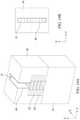
- FIGS. 6A and 6B are schematic illustrations of one of the stages of a sequential manufacturing operation of a semiconductor device according to an embodiment of the present disclosure.
- a substrate 5 is provide.
- the substrate 5 includes a single crystal semiconductor layer on at least its surface portion.
- the substrate 5 may comprise a single crystal semiconductor material such as, but not limited to Si, Ge, SiGe, GaAs, InSb, GaP, GaSb, InAlAs, InGaAs, GaSbP, GaAsSb and InP.
- the substrate 5 is made of crystalline Si, SiGe or Ge.
- the substrate 5 may include in its surface region, one or more buffer layers (not shown) in some embodiments.
- the buffer layers can serve to gradually change the lattice constant from that of the substrate to that of the source/drain regions.
- the buffer layers may be formed from epitaxially grown single crystal semiconductor materials such as, but not limited to Si, Ge, GeSn, SiGe, GaAs, InSb, GaP, GaSb, InAlAs, InGaAs, GaSbP, GaAsSb, GaN, GaP, and InP.
- the substrate 5 comprises silicon germanium (SiGe) buffer layers epitaxially grown on the silicon substrate 5 .
- the germanium concentration of the SiGe buffer layers may increase from 30 atomic % germanium for the bottom-most buffer layer to 70 atomic % germanium for the top-most buffer layer.
- first interlayer dielectric (ILD) layers 10 are formed over the substrate 5 .
- one or more electronic devices such as transistors (e.g., FETs), memories (e.g., dynamic random access memory (DRAM), static RAM, magnetic MRAM, and/or phase change RAM), are formed on the substrate 5 and the one or more first interlayer dielectric layers 10 cover the electronic devices.
- transistors e.g., FETs
- memories e.g., dynamic random access memory (DRAM), static RAM, magnetic MRAM, and/or phase change RAM
- one or more metal wiring structures are embedded in the ILD layers 10 .
- the dielectric material for the first ILD layers 10 includes silicon oxide, silicon nitride, silicon oxynitride (SiON), SiCN, fluorine-doped silicate glass (FSG), or a low-K dielectric material, formed by LPCVD (low pressure chemical vapor deposition), plasma-CVD or flowable CVD or any other suitable film formation method.
- An annealing operation may be performed after the formation of the first ILD layer 10 .
- a planarization operation such as a chemical mechanical polishing (CMP) method and/or an etch-back method, is performed to flatten the surface of the first ILD layer 10 .
- CMP chemical mechanical polishing
- FIGS. 7A and 7B are schematic illustrations of a sequential step of manufacturing a semiconductor device according to an embodiment of the present disclosure.
- semiconductor layers 25 and sacrificial layers 20 are alternately formed over the ILD layer 10 .
- the semiconductor layers 25 are made of oxide semiconductor materials, such as such as amorphous indium gallium zinc oxide (IGZO), c-axis aligned crystal (CAAC)-IGZO, ZnO, In 2 O 3 , Ga 2 O 3 , and ZnON. In some embodiments, amorphous IGZO is used.
- the semiconductor layers 25 are formed by CVD, atomic layer deposition (ALD), physical vapor deposition including sputtering, or any other suitable film formation method. In some embodiments, the semiconductor layers 25 are formed by CVD at a temperature in a range from about 50° C. to 600° C.
- the semiconductor layers 25 are formed by atomic layer deposition (ALD) at a temperature in a range from about 25° C. to 400° C. In some embodiments, the semiconductor layers 25 are formed by physical vapor deposition including sputtering at a temperature in a range from about 25° C. to 400° C.
- ALD atomic layer deposition
- the semiconductor layers 25 are formed by physical vapor deposition including sputtering at a temperature in a range from about 25° C. to 400° C.
- the sacrificial layers 20 are made of different material than the semiconductor layers 25 so that the sacrificial layers 20 are removed selective to the semiconductor layers 25 in the subsequent process.
- the sacrificial layer 25 are made of one or more layers of insulating materials, such as silicon oxide, silicon nitride, silicon oxynitride, SiOC, aluminum oxide, hafnium oxide or any other suitable insulating material.
- the sacrificial layers 25 are made of one or more layers of semiconductor material, such as Si, SiGe and Ge.
- the semiconductor layer is amorphous or polycrystalline.
- the sacrificial layers 25 are made of one or more layers of metallic material, such as metal nitride including TiN and TaN.
- the thickness of the semiconductor layers 25 is in a range from about 5 nm to about 30 nm, and is in a range from about 10 nm to about 20 nm in other embodiments. In some embodiments, the thickness of the sacrificial layers 20 is in a range from about 5 nm to about 30 nm, and is in a range from about 10 nm to about 20 nm in other embodiments. In some embodiments, the thickness of the semiconductor layers 25 is equal to the thickness of the sacrificial layers 20 , and in other embodiments, the thickness of the semiconductor layers 25 is greater or smaller than the thickness of the sacrificial layers 20 .
- a sacrificial layer 20 is directly formed on the first ILD layer 10 and the uppermost layer of the alternate stack is a sacrificial layer 20 . In other embodiments, the uppermost layer of the alternate stack is a semiconductor layer 25 .
- FIGS. 8A and 8B are schematic illustrations of a sequential step of manufacturing a semiconductor device according to an embodiment of the present disclosure.
- the alternate stack of the semiconductor layers 25 and sacrificial layers 20 is patterned into fin structures 22 .
- the fin structures 22 may be patterned by any suitable method.
- the structures may be patterned using one or more photolithography processes, including double-patterning or multi-patterning processes.
- double-patterning or multi-patterning processes combine photolithography and self-aligned processes, allowing patterns to be created that have, for example, pitches smaller than what is otherwise obtainable using a single, direct photolithography process.
- a sacrificial layer (a mandrel pattern) is formed over a substrate and patterned using a photolithography process. Spacers are formed alongside the patterned sacrificial layer using a self-aligned process. The sacrificial layer (mandrel pattern) is then removed, and the remaining spacers may then be used to pattern the fin structure 22 .
- the number of the fin structures for one TFT is not limited to five. In some embodiments, the number of the fin structures per TFT ranges from 1 to 10 and is in a range from 2 to 5 in other embodiments, depending on driving current requirements.
- a width of the fin structures 25 is in a range from about 10 nm to about 50 nm in some embodiments, and is in a range from about 15 nm to about 30 nm in other embodiments.
- FIGS. 9A and 9B are schematic illustrations of a sequential step of manufacturing a semiconductor device according to an embodiment of the present disclosure.
- a sacrificial gate dielectric layer 42 is formed over the fin structures 22 and the ILD layer 20 as shown in FIG. 9A .
- the sacrificial gate dielectric layer 42 is made of insulating material such as silicon oxide, silicon nitride, silicon oxynitride, SiOC, aluminum oxide, hafnium oxide or any other suitable insulating material. In other embodiments, no sacrificial gate dielectric layer is formed.
- FIGS. 10A and 10B are schematic illustrations of a sequential step of manufacturing a semiconductor device according to an embodiment of the present disclosure. Then, a sacrificial gate structure 40 for a gate replacement technique is formed as shown in FIGS. 10A and 10B .
- the sacrificial gate structure includes a sacrificial gate electrode layer 44 and a hard mask layer 46 .
- the sacrificial gate electrode layer 44 is polycrystalline or amorphous Si, SiGe or Ge.
- the sacrificial gate electrode layer 44 is formed by chemical vapor deposition (CVD) or any other suitable film formation methods, and a hard mask layer 46 is formed over the sacrificial gate electrode layer 44 .
- the hard mask layer 46 is made of a silicon nitride based material, such as silicon nitride, SiON or SiCN or a silicon oxide based material, such as silicon oxide. After the hard mask layer 46 is formed, by using one or more lithography and etching operations, the hard mask layer 46 is patterned. Then, by using the patterned hard mask layer 46 as an etching mask, the deposited sacrificial gate electrode layer 44 is patterned. In some embodiments, one or more dummy gate structures for suppressing process variations and/or to improve pattern fidelity are formed to surround the sacrificial gate structures for a functional transistor.
- FIGS. 11A and 11B are schematic illustrations of a sequential step of manufacturing a semiconductor device according to an embodiment of the present disclosure. Subsequently, as shown in FIGS. 11A and 11B , gate sidewall spacers 48 are formed on side faces of the sacrificial gate structure 40 .
- a blanket layer of an insulating material for first sidewall spacers is conformally formed by using CVD or other suitable methods. The blanket layer is deposited in a conformal manner so that it is formed to have substantially equal thicknesses on vertical surfaces, such as the sidewalls, horizontal surfaces, and the top of the sacrificial gate structure 40 . In some embodiments, the blanket layer is deposited to a thickness in a range from about 2 nm to about 30 nm.
- the insulating material of the blanket layer is different from the materials of the sacrificial gate structure, and is made of a silicon nitride-based material, such as silicon nitride, SiON, SiOCN or SiCN and combinations thereof.
- the blanket layer is made of silicon nitride.
- the sidewall spacers are formed on opposite side faces of the sacrificial gate structure, by anisotropic etching.
- the gate side wall spacers 48 are formed on opposing side faces of the hard mask layer 46 .
- sidewall spacers are formed on side faces of the fin structures 22 .
- FIGS. 12A and 12B are schematic illustrations of a sequential step of manufacturing a semiconductor device according to an embodiment of the present disclosure. Then, the sacrificial gate dielectric layer 42 is removed and the fin structures 22 are exposed, as shown in FIGS. 12A and 12B . As shown in FIG. 12A , the sacrificial gate dielectric layer 42 remains under the sacrificial gate structure 40 and the gate sidewall spacers 48 .
- FIGS. 13A and 13B are schematic illustrations of a sequential step of manufacturing a semiconductor device according to an embodiment of the present disclosure.
- a second ILD layer 50 is formed over the sacrificial gate structure 40 and the fin structures 22 , as shown in FIGS. 13A and 13B .
- the materials for the second ILD layer 50 include compounds comprising Si, O, C and/or H, such as silicon oxide, SiCOH and SiOC. Organic materials, such as polymers, may be used for the second ILD layer 50 .
- the second ILD layer 50 is made of the same material as the first ILD layer 10 .
- a planarization operation such as CMP, is performed, so that the top portion of the sacrificial gate electrode layer 44 is exposed, as shown in FIGS. 13A and 13B .
- FIGS. 14A and 14B are schematic illustrations of a sequential step of manufacturing a semiconductor device according to an embodiment of the present disclosure.
- the sacrificial gate electrode layer 44 and the sacrificial gate dielectric layer 42 are removed, thereby forming a gate space 52 , as shown in FIGS. 14A and 14B .
- the sacrificial gate electrode layer 44 can be removed using plasma dry etching and/or wet etching.
- TMAH tetramethylammonium hydroxide solution
- the sacrificial gate dielectric layer 42 is also removed by suitable wet/dry etching.
- the sacrificial layers 20 are also removed under the gate space 52 .
- the removal operation e.g., wet etching
- the sacrificial layers 20 and the sacrificial gate dielectric layer 42 are made of the same or similar materials, the removal operation (e.g., wet etching) of the sacrificial gate dielectric layer 42 also removes the sacrificial layer 20 .
- two or more etching operations are performed to remove the sacrificial gate dielectric layer 42 and the sacrificial layers 20 sequentially. By removing the sacrificial layers 20 , channel regions of the semiconductor layers 25 are released in the gate space 52 as semiconductor nano-sheets.
- FIGS. 15A and 15B are schematic illustrations of a sequential step of manufacturing a semiconductor device according to an embodiment of the present disclosure. Then, as shown in FIGS. 15A and 15B , a gate dielectric layer 82 and a gate electrode layer 80 are formed in the gate space 52 .
- the gate dielectric layer 82 includes one or more layers of a dielectric material, such as silicon oxide, silicon nitride, or a high-k dielectric material, other suitable dielectric material, and/or combinations thereof.
- high-k dielectric materials include HfO 2 , HfSiO, HfSiON, HfTaO, HfTiO, HfZrO, zirconium oxide, aluminum oxide, titanium oxide, hafnium dioxide-alumina (HfO 2 -Al 2 O 3 ) alloy, other suitable high-k dielectric materials, and/or combinations thereof.
- the gate dielectric layer 82 includes an interfacial layer formed between the channel region and the dielectric material.
- the gate dielectric layer 82 may be formed by CVD, ALD or any suitable methods.
- the gate dielectric layer 82 is formed using a highly conformal deposition process such as ALD in order to ensure the formation of a gate dielectric layer having a uniform thickness around each channel region.
- the thickness of the gate dielectric layer 82 is in a range from about 1 nm to about 20 nm in some embodiments and is in a range from about 2 nm to about 10 nm in other embodiments.
- the metal gate electrode layer 80 includes one or more work function adjustment layers 84 and a body metal gate electrode layer 86 in some embodiments.
- the work function adjustment layers are made of a conductive material such as a single layer of TiN, TaN, TaAlC, TiC, TaC, Co, Al, TiAl, HfTi, TiSi, TaSi or TiAlC, or a multilayer of two or more of these materials.
- the work function adjustment layer may be formed by ALD, PVD, CVD, e-beam evaporation, or other suitable process. Further, the work function adjustment layer 84 may be formed separately for the nFET and the pFET, which may use different metal layers.
- the body gate electrode layer is formed to surround each oxide semiconductor nano-sheet (channel region).
- the body gate electrode layer includes one or more layers of conductive material, such as polysilicon, aluminum, copper, titanium, tantalum, tungsten, cobalt, molybdenum, tantalum nitride, nickel silicide, cobalt silicide, TiN, WN, TiAl, TiAlN, TaCN, TaC, TaSiN, metal alloys, other suitable materials, and/or combinations thereof.
- the body gate electrode layer may be formed by CVD, ALD, electro-plating, or other suitable method.
- the metals for the gate dielectric layer 82 and the gate electrode layer 80 are also deposited over the upper surface of the second ILD layer 50 .
- the material for the gate electrode layer 80 formed over the second ILD layer 50 is then planarized by using, for example, CMP, until the top surface of the second ILD layer 50 is revealed, as shown in FIGS. 15A and 15B .
- the metal gate electrode layer is recessed and a cap insulating layer (not shown) is formed over the recessed gate electrode layer.
- the cap insulating layer includes one or more layers of a silicon nitride-based material, such as silicon nitride.
- the cap insulating layer can be formed by depositing an insulating material followed by a planarization operation.
- FIGS. 16A and 16B are schematic illustrations of a sequential step of manufacturing a semiconductor device according to an embodiment of the present disclosure.
- a third ILD layer 60 is formed over the second ILD layer 50 , and contact holes 65 for source/drain contact are formed in the third and second ILD layers, as shown in FIGS. 16A and 16B .
- the materials for the third ILD layer 60 include compounds comprising Si, O, C and/or H, such as silicon oxide, SiCOH and SiOC. Organic materials, such as polymers, may be used for the third ILD layer 60 .
- the third ILD layer 60 is made of the same material as the second ILD layer and/or the first ILD layer 10 .
- the third ILD layer 60 functions as a hard mask layer for etching the second ILD layer.
- FIGS. 17A and 17B are schematic illustrations of a sequential step of manufacturing a semiconductor device according to an embodiment of the present disclosure. After the contact holes 65 are formed, the sacrificial layers 20 are removed under the contact holes 65 , thereby source/drain regions of the semiconductor layers 20 are released, as shown in FIG. 17A .
- part of the sacrificial layers 20 remain as inner spacers 21 .
- the sacrificial layers 20 are made of an insulating material in some embodiments. In other embodiments, the sacrificial layers 20 are fully removed.
- FIGS. 18A-20B are schematic illustrations of a sequential step of manufacturing a semiconductor device according to an embodiment of the present disclosure.
- FIG. 18A shows a cross section cutting along the source-to-drain direction (Y direction)
- FIG. 19A shows a cross section cutting along the gate extending direction (X direction) of the gate electrode
- FIG. 20 A shows a cross section cutting along the X direction of a source/drain contact.
- source/drain contacts 70 are formed in the contact holes 65 .
- One or more layers of conductive materials are formed in and over the contact holes then a planarization operation, such as a CMP operation, is performed to form conductive contacts 70 .
- the source/drain contact 70 includes a liner or a barrier layer 72 and a body contact layer 74 , as shown in FIG. 4 .
- the liner layer 72 is made of one or more of Ti, TiN, Ta, and TaN
- the body contact layer 74 is made of one or more of W, Cu, Ti, Ag, Al, Mn, Co, Pd, Ni, Re, Jr, Ru, Pt, and Zr.
- at least the liner layer 72 wraps around the source/drain regions of the semiconductor layers (nano-sheet) 25 .
- the body contact layer 74 also wraps around the source/drain regions.
- TFT undergoes further processes to form various features such as contacts/vias, interconnect metal layers, dielectric layers, passivation layers, etc.
- FIGS. 21A-22B shows sequential operations for manufacturing a semiconductor device according to another embodiment of the present disclosure. It is understood that additional operations can be provided before, during, and after the processes shown by FIGS. 21A-22B , and some of the operations described below can be replaced or eliminated, for additional embodiments of the method.
- the manufacturing operations shown in FIGS. 21A-22B correspond to the TFT structure shown in FIG. 5 .
- both the semiconductor layer 25 and the sacrificial layers 20 are removed in the contact holes 65 , as shown in FIGS. 21A and 21B .
- source/drain contacts 70 are formed, as shown in FIGS. 22A and 22B .
- FIG. 23 shows a cross sectional view of a semiconductor device according to an embodiment of the present disclosure.
- a lower layer device 100 is formed over a substrate.
- the lower layer devices 100 includes one or more fin field effect transistors (FinFETs), gate-all-around FET (GAA FET), planar FETs, vertical FETs or any other electronic devices.
- FIG. 23 also shows an upper layer device 200 disposed over the lower layer device 100 .
- one or more ILD layers, metal wiring layers and/or via contacts are disposed between the lower layer device 100 and the upper layer device 200 .
- the upper layer device 200 includes one or more TFTs manufactured by the aforementioned embodiments of the present disclosure.
- a power switching circuit for switching power supply from the main power supply (VDD or VSS) to the local power supply (VVDD or VVSS) and power supply wirings are formed by using an oxide semiconductor such as IGZO. Accordingly, it is possible to provide the power switching circuit at the BEOL circuit level.
- a stacked structure including semiconductor layers and sacrificial layers are alternately stacked is formed, a sacrificial gate structure is formed over the stacked structure, a dielectric layer is formed over the sacrificial gate structure, the sacrificial gate structure is removed, thereby forming a gate space, the sacrificial layers are removed in the gate space, thereby releasing the semiconductor layers, a gate structure wrapping around the semiconductor layers is formed.
- the semiconductor layers are made of an oxide semiconductor material.
- the oxide semiconductor material includes one selected from the group consisting of indium gallium zinc oxide (IGZO), c-axis aligned crystal (CAAC)-IGZO, ZnO, In 2 O 3 , Ga 2 O 3 , and ZnON.
- the oxide semiconductor material includes amorphous indium gallium zinc oxide (IGZO).
- the sacrificial layer includes one selected from the group consisting of an insulating material, an amorphous or polycrystalline semiconductor material, and a metal nitride material.
- the stacked structure is formed on an insulating material layer.
- the insulating material layer covers transistors formed over a semiconductor substrate.
- the stacked structure is formed by alternately forming the semiconductor layers and the sacrificial layers on an insulating material layer, and patterning the semiconductor layers and the sacrificial layers into one or more fin structures.
- a fin structure including semiconductor layers and sacrificial layers are alternately stacked is formed over a first dielectric layer, a sacrificial gate structure is formed over the fin structure, gate sidewall spacers are formed on opposing side faces of the sacrificial gate structure, a second dielectric layer is formed over the sacrificial gate structure and the fin structure, the sacrificial gate structure are removed, thereby forming a gate space, the sacrificial layers are removed in the gate space, thereby releasing channel regions of the semiconductor layers, a gate structure wrapping around the channel regions of the semiconductor layers is formed, a third dielectric layer is formed, a contact opening is formed in the third dielectric layer and the second dielectric layer, the sacrificial layers are removed in the contact opening, thereby releasing source/drain regions of the semiconductor layers, and a source/drain contact wrapping around the source/drain regions of the semiconductor layers is formed.
- the semiconductor layers are made of an oxide semiconductor material.
- the oxide semiconductor material includes one selected from the group consisting of indium gallium zinc oxide (IGZO), c-axis aligned crystal (CAAC)-IGZO, ZnO, In 2 O 3 , Ga 2 O 3 , and ZnON.
- the oxide semiconductor material includes amorphous indium gallium zinc oxide (IGZO).
- the sacrificial layer includes one selected from the group consisting of as silicon oxide, silicon nitride, silicon oxynitride, SiOC, aluminum oxide, hafnium oxide.
- the sacrificial layer includes one selected from the group consisting of amorphous or polycrystalline Si, SiGe and Ge. In one or more of the foregoing and/or following embodiments, the sacrificial layer includes one selected from the group consisting of TiN and TaN. In one or more of the foregoing and/or following embodiments, the first dielectric layer covers transistors formed over a semiconductor substrate.
- the remaining parts of the sacrificial layers are disposed between the source/drain contact and the gate structure.
- a fin structure including semiconductor layers and sacrificial layers are alternately stacked is formed over a first dielectric layer, a sacrificial gate structure is formed over the fin structure, gate sidewall spacers are formed on opposing side faces of the sacrificial gate structure, a second dielectric layer is formed over the sacrificial gate structure and the fin structure, the sacrificial gate structure is removed, thereby forming a gate space, the sacrificial layers are removed in the gate space, thereby releasing channel regions of the semiconductor layers, a gate structure wrapping around the channel regions of the semiconductor layers is formed, a third dielectric layer is formed, a contact opening is formed in the third dielectric layer and the second dielectric layer, the sacrificial layers and the semiconductor layer are removed in the contact opening, and a source/drain contact is formed in the contact opening.
- the semiconductor layers are made of an oxide semiconductor material.
- the oxide semiconductor material includes one selected from the group consisting of indium gallium zinc oxide (IGZO), c-axis aligned crystal (CAAC)-IGZO, ZnO, In 2 O 3 , Ga 2 O 3 , and ZnON.
- the oxide semiconductor material includes amorphous indium gallium zinc oxide (IGZO).
- the sacrificial layer includes one selected from the group consisting of as silicon oxide, silicon nitride, silicon oxynitride, SiOC, aluminum oxide, hafnium oxide.
- the remaining parts of the sacrificial layers are disposed between the source/drain contact and the gate structure.
- a semiconductor device includes a power switch circuit and a logic circuit.
- the semiconductor device includes a first dielectric layer and a thin film transistor (TFT) formed on the first dielectric layer.
- the TFT includes a semiconductor nano-sheet, a gate dielectric layer wrapping around a channel region of the semiconductor nano-sheet, and a gate electrode layer formed on the gate dielectric layer.
- the semiconductor nano-sheet is made of an oxide semiconductor material.
- the oxide semiconductor material includes one selected from the group consisting of indium gallium zinc oxide (IGZO), c-axis aligned crystal (CAAC)-IGZO, ZnO, In 2 O 3 , Ga 2 O 3 , and ZnON.
- the oxide semiconductor material includes amorphous indium gallium zinc oxide (IGZO).
- IGZO amorphous indium gallium zinc oxide
- a thickness T 1 of the semiconductor nano-sheet is in a range from 5 nm to 30 nm
- a width W 1 of each of the semiconductor nano-sheets along a gate extending direction is in a range from 10 nm to 50 nm.
- a ratio W 1 /T 1 is in a range from 1.2 to 10.
- a semiconductor device includes a power switch circuit and a logic circuit.
- the power switch circuit includes a first dielectric layer and a thin film transistor (TFT) formed on the first dielectric layer.
- TFT thin film transistor
- the TFT includes semiconductor nano-sheets vertically arranged, a gate dielectric layer wrapping around a channel region of each of the semiconductor nano-sheets, and a gate electrode layer formed on the gate dielectric layer.
- the semiconductor nano-sheets are made of an oxide semiconductor material.
- the oxide semiconductor material includes one selected from the group consisting of indium gallium zinc oxide (IGZO), c-axis aligned crystal (CAAC)-IGZO, ZnO, In 2 O 3 , Ga 2 O 3 , and ZnON. In one or more of the foregoing and/or following embodiments, the oxide semiconductor material includes amorphous indium gallium zinc oxide (IGZO).
- a thickness T 1 of each of the semiconductor nano-sheets is in a range from 5 nm to 30 nm, and a width W 1 of each of the semiconductor nano-sheets along a gate extending direction is in a range from 10 nm to 50 nm.
- a ratio W 1 /T 1 is in a range from 2 to 5.
- a number of the semiconductor nano-sheets is in a range from 2 to 10.
- the TFT further includes a source/drain contact wrapping around a source/drain region of each of the semiconductor nano-sheets. In one or more of the foregoing and/or following embodiments, the TFT further includes inner spacers disposed between the source/drain contact and the gate electrode layer. In one or more of the foregoing and/or following embodiments, the TFT further includes a source/drain contact in contact with end faces of the semiconductor nano-sheets. In one or more of the foregoing and/or following embodiments, the TFT further includes inner spacers disposed between the source/drain contact and the gate electrode layer.
- a semiconductor device including a power switch circuit and a logic circuit, and the semiconductor device includes a first dielectric layer, and a thin film transistor (TFT) formed on the first dielectric layer.
- the TFT includes a plurality of groups of semiconductor nano-sheets, wherein the semiconductor nano-sheets are vertically arranged in each of the plurality of groups, a gate dielectric layer wrapping around a channel region of each of the semiconductor nano-sheets of the plurality of groups of semiconductor nano-sheets, and a gate electrode layer formed on the gate dielectric layer over the plurality of groups of semiconductor nano-sheets.
- the the semiconductor nano-sheets are made of an oxide semiconductor material.
- the oxide semiconductor material includes amorphous indium gallium zinc oxide (IGZO).
- IGZO amorphous indium gallium zinc oxide
- a thickness T 1 of each of the semiconductor nano-sheets is in a range from 5 nm to 30 nm
- a width W 1 of each of the semiconductor nano-sheets along a gate extending direction is in a range from 10 nm to 50 nm.
- a number of the semiconductor nano-sheets is in a range from 2 to 10.
- a number of the plurality of groups is in a range from 2 to 5.
Landscapes
- Engineering & Computer Science (AREA)
- Power Engineering (AREA)
- Microelectronics & Electronic Packaging (AREA)
- Physics & Mathematics (AREA)
- Condensed Matter Physics & Semiconductors (AREA)
- General Physics & Mathematics (AREA)
- Computer Hardware Design (AREA)
- Ceramic Engineering (AREA)
- Manufacturing & Machinery (AREA)
- Chemical & Material Sciences (AREA)
- Nanotechnology (AREA)
- Crystallography & Structural Chemistry (AREA)
- Materials Engineering (AREA)
- Mathematical Physics (AREA)
- Theoretical Computer Science (AREA)
- Thin Film Transistor (AREA)
- Insulated Gate Type Field-Effect Transistor (AREA)
- Encapsulation Of And Coatings For Semiconductor Or Solid State Devices (AREA)
Abstract
Description
Claims (20)
Priority Applications (6)
| Application Number | Priority Date | Filing Date | Title |
|---|---|---|---|
| US16/658,768 US11264506B2 (en) | 2018-10-31 | 2019-10-21 | Semiconductor device and manufacturing method thereof |
| DE102019128703.0A DE102019128703A1 (en) | 2018-10-31 | 2019-10-24 | SEMICONDUCTOR DEVICE AND PRODUCTION METHOD |
| TW108139131A TWI787553B (en) | 2018-10-31 | 2019-10-29 | Semiconductor device and manufacturing method thereof |
| CN201911055398.8A CN111199886B (en) | 2018-10-31 | 2019-10-31 | Semiconductor device and method for manufacturing the same |
| KR1020190137257A KR102330560B1 (en) | 2018-10-31 | 2019-10-31 | Semiconductor device and manufacturing method thereof |
| US17/682,087 US20220181491A1 (en) | 2018-10-31 | 2022-02-28 | Semiconductor device and manufacturing method thereof |
Applications Claiming Priority (2)
| Application Number | Priority Date | Filing Date | Title |
|---|---|---|---|
| US201862753890P | 2018-10-31 | 2018-10-31 | |
| US16/658,768 US11264506B2 (en) | 2018-10-31 | 2019-10-21 | Semiconductor device and manufacturing method thereof |
Related Child Applications (1)
| Application Number | Title | Priority Date | Filing Date |
|---|---|---|---|
| US17/682,087 Division US20220181491A1 (en) | 2018-10-31 | 2022-02-28 | Semiconductor device and manufacturing method thereof |
Publications (2)
| Publication Number | Publication Date |
|---|---|
| US20200135929A1 US20200135929A1 (en) | 2020-04-30 |
| US11264506B2 true US11264506B2 (en) | 2022-03-01 |
Family
ID=70327429
Family Applications (2)
| Application Number | Title | Priority Date | Filing Date |
|---|---|---|---|
| US16/658,768 Active US11264506B2 (en) | 2018-10-31 | 2019-10-21 | Semiconductor device and manufacturing method thereof |
| US17/682,087 Pending US20220181491A1 (en) | 2018-10-31 | 2022-02-28 | Semiconductor device and manufacturing method thereof |
Family Applications After (1)
| Application Number | Title | Priority Date | Filing Date |
|---|---|---|---|
| US17/682,087 Pending US20220181491A1 (en) | 2018-10-31 | 2022-02-28 | Semiconductor device and manufacturing method thereof |
Country Status (5)
| Country | Link |
|---|---|
| US (2) | US11264506B2 (en) |
| KR (1) | KR102330560B1 (en) |
| CN (1) | CN111199886B (en) |
| DE (1) | DE102019128703A1 (en) |
| TW (1) | TWI787553B (en) |
Families Citing this family (7)
| Publication number | Priority date | Publication date | Assignee | Title |
|---|---|---|---|---|
| DE102020119963A1 (en) | 2020-01-30 | 2021-08-05 | Taiwan Semiconductor Manufacturing Co., Ltd. | SEMICONDUCTOR DEVICE AND METHOD |
| TW202130846A (en) * | 2020-02-03 | 2021-08-16 | 荷蘭商Asm Ip私人控股有限公司 | Method of forming structures including a vanadium or indium layer |
| US11658220B2 (en) | 2020-04-24 | 2023-05-23 | Taiwan Semiconductor Manufacturing Company, Ltd. | Drain side recess for back-side power rail device |
| US11581224B2 (en) * | 2020-05-08 | 2023-02-14 | Taiwan Semiconductor Manufacturing Company, Ltd. | Method for forming long channel back-side power rail device |
| DE102021109149A1 (en) * | 2020-05-28 | 2021-12-02 | Taiwan Semiconductor Manufacturing Co. Ltd. | ADVANTAGE FIELD EFFECT TRANSISTOR AND ITS MANUFACTURING PROCESS |
| US20210398977A1 (en) * | 2020-06-18 | 2021-12-23 | Intel Corporation | Double-sided integrated circuit transistor structures with depopulated bottom channel regions |
| US11653581B2 (en) * | 2020-08-13 | 2023-05-16 | Taiwan Semiconductor Manufacturing Co., Ltd. | RRAM device structure and manufacturing method |
Citations (15)
| Publication number | Priority date | Publication date | Assignee | Title |
|---|---|---|---|---|
| US20050272231A1 (en) * | 2004-06-08 | 2005-12-08 | Eun-Jung Yun | Gate-all-around type of semiconductor device and method of fabricating the same |
| US20070158679A1 (en) * | 2005-12-31 | 2007-07-12 | Samsung Electronics Co., Ltd. | Semiconductor device with multiple channels and method of fabricating the same |
| US20110175646A1 (en) | 2010-01-20 | 2011-07-21 | Semiconductor Energy Laboratory Co., Ltd. | Semiconductor device |
| US20120138886A1 (en) | 2010-12-01 | 2012-06-07 | Kuhn Kelin J | Silicon and silicon germanium nanowire structures |
| US20140001441A1 (en) | 2012-06-29 | 2014-01-02 | Seiyon Kim | Integration methods to fabricate internal spacers for nanowire devices |
| US20140017890A1 (en) | 2012-07-12 | 2014-01-16 | International Business Machines Corporation | Replacement Contacts for All-Around Contacts |
| KR20160061876A (en) | 2014-11-24 | 2016-06-01 | 인텔 코포레이션 | Electrode configurations to increase electro-thermal isolation of phase-change memory elements and associated techniques |
| US20170140996A1 (en) * | 2015-11-16 | 2017-05-18 | Taiwan Semiconductor Manufacturing Company, Ltd. | Horizontal Gate-All-Around Device Having Wrapped-Around Source and Drain |
| US20170154958A1 (en) | 2015-11-30 | 2017-06-01 | Taiwan Semiconductor Manufacturing Co., Ltd. | Semiconductor device and manufacturing method thereof |
| WO2017111797A1 (en) | 2015-12-23 | 2017-06-29 | Intel Corporation | Fabrication of non-planar igzo devices for improved electrostatics |
| JP2018164085A (en) | 2017-03-27 | 2018-10-18 | 三星電子株式会社Samsung Electronics Co.,Ltd. | Memory element including variable resistance material layer |
| US20190131437A1 (en) * | 2016-06-30 | 2019-05-02 | Intel Corporation | Integrated circuit die having back-end-of-line transistors |
| US20190333990A1 (en) * | 2017-03-30 | 2019-10-31 | Intel Corporation | Removal of a bottom-most nanowire from a nanowire device stack |
| US20200006388A1 (en) * | 2018-06-29 | 2020-01-02 | Intel Corporation | Transistors stacked on front-end p-type transistors |
| US20200091288A1 (en) * | 2018-09-18 | 2020-03-19 | International Business Machines Corporation | Inner spacer formation and contact resistance reduction in nanosheet transistors |
Family Cites Families (14)
| Publication number | Priority date | Publication date | Assignee | Title |
|---|---|---|---|---|
| JPH08280142A (en) * | 1995-04-07 | 1996-10-22 | Sony Corp | Power supply switch circuit |
| KR101377597B1 (en) * | 2007-03-21 | 2014-03-27 | 삼성디스플레이 주식회사 | Transistor and method of manufacturing the same |
| US8685850B2 (en) * | 2011-06-13 | 2014-04-01 | Stmicroelectronics, Inc. | System and method of plating conductive gate contacts on metal gates for self-aligned contact interconnections |
| TWI664731B (en) * | 2013-05-20 | 2019-07-01 | 半導體能源研究所股份有限公司 | Semiconductor device |
| US9722049B2 (en) * | 2013-12-23 | 2017-08-01 | Intermolecular, Inc. | Methods for forming crystalline IGZO with a seed layer |
| US10050147B2 (en) * | 2015-07-24 | 2018-08-14 | Taiwan Semiconductor Manufacturing Co., Ltd. | Semiconductor device and manufacturing method thereof |
| US9583399B1 (en) * | 2015-11-30 | 2017-02-28 | Taiwan Semiconductor Manufacturing Co., Ltd. | Semiconductor device and manufacturing method thereof |
| EP3394895A1 (en) * | 2015-12-23 | 2018-10-31 | Intel Corporation | Fabrication of wrap-around and conducting metal oxide contacts for igzo non-planar devices |
| KR102483546B1 (en) * | 2016-11-28 | 2023-01-02 | 삼성전자주식회사 | Semiconductor devices having a vertical channel |
| CN108172625B (en) * | 2016-12-07 | 2020-09-29 | 清华大学 | Logic circuit |
| CN106756877B (en) * | 2016-12-13 | 2019-02-19 | 武汉华星光电技术有限公司 | C axis crystallizes IGZO film and preparation method thereof |
| US10170584B2 (en) * | 2017-01-27 | 2019-01-01 | International Business Machines Corporation | Nanosheet field effect transistors with partial inside spacers |
| US10297663B2 (en) * | 2017-04-19 | 2019-05-21 | International Business Machines Corporation | Gate fill utilizing replacement spacer |
| US11380684B2 (en) * | 2018-09-28 | 2022-07-05 | Intel Corporation | Stacked transistor architecture including nanowire or nanoribbon thin film transistors |
-
2019
- 2019-10-21 US US16/658,768 patent/US11264506B2/en active Active
- 2019-10-24 DE DE102019128703.0A patent/DE102019128703A1/en active Pending
- 2019-10-29 TW TW108139131A patent/TWI787553B/en active
- 2019-10-31 CN CN201911055398.8A patent/CN111199886B/en active Active
- 2019-10-31 KR KR1020190137257A patent/KR102330560B1/en active IP Right Grant
-
2022
- 2022-02-28 US US17/682,087 patent/US20220181491A1/en active Pending
Patent Citations (16)
| Publication number | Priority date | Publication date | Assignee | Title |
|---|---|---|---|---|
| US20050272231A1 (en) * | 2004-06-08 | 2005-12-08 | Eun-Jung Yun | Gate-all-around type of semiconductor device and method of fabricating the same |
| US20070158679A1 (en) * | 2005-12-31 | 2007-07-12 | Samsung Electronics Co., Ltd. | Semiconductor device with multiple channels and method of fabricating the same |
| US20110175646A1 (en) | 2010-01-20 | 2011-07-21 | Semiconductor Energy Laboratory Co., Ltd. | Semiconductor device |
| US20120138886A1 (en) | 2010-12-01 | 2012-06-07 | Kuhn Kelin J | Silicon and silicon germanium nanowire structures |
| US20140001441A1 (en) | 2012-06-29 | 2014-01-02 | Seiyon Kim | Integration methods to fabricate internal spacers for nanowire devices |
| US20140017890A1 (en) | 2012-07-12 | 2014-01-16 | International Business Machines Corporation | Replacement Contacts for All-Around Contacts |
| KR20160061876A (en) | 2014-11-24 | 2016-06-01 | 인텔 코포레이션 | Electrode configurations to increase electro-thermal isolation of phase-change memory elements and associated techniques |
| US20170140996A1 (en) * | 2015-11-16 | 2017-05-18 | Taiwan Semiconductor Manufacturing Company, Ltd. | Horizontal Gate-All-Around Device Having Wrapped-Around Source and Drain |
| US20170154958A1 (en) | 2015-11-30 | 2017-06-01 | Taiwan Semiconductor Manufacturing Co., Ltd. | Semiconductor device and manufacturing method thereof |
| WO2017111797A1 (en) | 2015-12-23 | 2017-06-29 | Intel Corporation | Fabrication of non-planar igzo devices for improved electrostatics |
| US20180366587A1 (en) * | 2015-12-23 | 2018-12-20 | Intel Corporation | Fabrication of non-planar igzo devices for improved electrostatics |
| US20190131437A1 (en) * | 2016-06-30 | 2019-05-02 | Intel Corporation | Integrated circuit die having back-end-of-line transistors |
| JP2018164085A (en) | 2017-03-27 | 2018-10-18 | 三星電子株式会社Samsung Electronics Co.,Ltd. | Memory element including variable resistance material layer |
| US20190333990A1 (en) * | 2017-03-30 | 2019-10-31 | Intel Corporation | Removal of a bottom-most nanowire from a nanowire device stack |
| US20200006388A1 (en) * | 2018-06-29 | 2020-01-02 | Intel Corporation | Transistors stacked on front-end p-type transistors |
| US20200091288A1 (en) * | 2018-09-18 | 2020-03-19 | International Business Machines Corporation | Inner spacer formation and contact resistance reduction in nanosheet transistors |
Non-Patent Citations (2)
| Title |
|---|
| Shao Hui Wu, "Performance Boost of Crystalline In—Ga—Zn—O Material and Transistor with Extremely Low Leakage for IoT Normally-Off CPU Application", 2017 Symposium on VLSI Technology Digest of Technical Papers. T166-T167. |
| Shunpei Yamazaki, "Unique Technology from Japan to the World—Super Low Power LSI using CAAC-OS-" Semiconductor Energy Laboratory presentation (May 27, 2015). |
Also Published As
| Publication number | Publication date |
|---|---|
| TW202025498A (en) | 2020-07-01 |
| KR102330560B1 (en) | 2021-11-26 |
| US20220181491A1 (en) | 2022-06-09 |
| KR20200050422A (en) | 2020-05-11 |
| TWI787553B (en) | 2022-12-21 |
| US20200135929A1 (en) | 2020-04-30 |
| CN111199886B (en) | 2022-11-01 |
| DE102019128703A1 (en) | 2020-04-30 |
| CN111199886A (en) | 2020-05-26 |
Similar Documents
| Publication | Publication Date | Title |
|---|---|---|
| US11264506B2 (en) | Semiconductor device and manufacturing method thereof | |
| US11848242B2 (en) | Method of manufacturing a semiconductor device and a semiconductor device | |
| US11728222B2 (en) | Complementary MOS FETS vertically arranged and including multiple dielectric layers surrounding the MOS FETS | |
| US11682587B2 (en) | Semiconductor device and manufacturing method thereof | |
| US10083972B2 (en) | Hybrid logic and SRAM contacts | |
| CN109427905A (en) | The method and semiconductor devices of manufacturing semiconductor devices | |
| US11600616B2 (en) | Semiconductor device including FINFETs having different channel heights | |
| US11177179B2 (en) | Method of manufacturing a semiconductor device and a semiconductor device | |
| US11152213B2 (en) | Transistor device with ultra low-k self aligned contact cap and ultra low-k spacer | |
| CN110970360B (en) | Semiconductor device and method for manufacturing semiconductor device | |
| US20210408049A1 (en) | Semiconductor chip | |
| KR102390076B1 (en) | Method of manufacturing a semiconductor device and a semiconductor device | |
| US20220336679A1 (en) | Semiconductor structure with barrier and method for manufacturing the same | |
| US20240030310A1 (en) | Semiconductor device and method for forming the same | |
| US11955561B2 (en) | Carrier modification devices for avoiding channel length reduction and methods for fabricating the same | |
| US20230062842A1 (en) | Structure and Method for MRAM Devices | |
| US20230053595A1 (en) | Field effect transistor with multi-metal gate via and method |
Legal Events
| Date | Code | Title | Description |
|---|---|---|---|
| FEPP | Fee payment procedure |
Free format text: ENTITY STATUS SET TO UNDISCOUNTED (ORIGINAL EVENT CODE: BIG.); ENTITY STATUS OF PATENT OWNER: LARGE ENTITY |
|
| AS | Assignment |
Owner name: TAIWAN SEMICONDUCTOR MANUFACTURING CO., LTD., TAIWAN Free format text: ASSIGNMENT OF ASSIGNORS INTEREST;ASSIGNORS:VAN DAL, MARCUS JOHANNES HENRICUS;DOORNBOS, GERBEN;REEL/FRAME:052299/0782 Effective date: 20191022 |
|
| STPP | Information on status: patent application and granting procedure in general |
Free format text: RESPONSE TO NON-FINAL OFFICE ACTION ENTERED AND FORWARDED TO EXAMINER |
|
| STPP | Information on status: patent application and granting procedure in general |
Free format text: NON FINAL ACTION MAILED |
|
| STPP | Information on status: patent application and granting procedure in general |
Free format text: RESPONSE TO NON-FINAL OFFICE ACTION ENTERED AND FORWARDED TO EXAMINER |
|
| STPP | Information on status: patent application and granting procedure in general |
Free format text: FINAL REJECTION MAILED |
|
| STPP | Information on status: patent application and granting procedure in general |
Free format text: RESPONSE AFTER FINAL ACTION FORWARDED TO EXAMINER |
|
| STPP | Information on status: patent application and granting procedure in general |
Free format text: NOTICE OF ALLOWANCE MAILED -- APPLICATION RECEIVED IN OFFICE OF PUBLICATIONS Free format text: AWAITING TC RESP., ISSUE FEE NOT PAID |
|
| STPP | Information on status: patent application and granting procedure in general |
Free format text: PUBLICATIONS -- ISSUE FEE PAYMENT VERIFIED |
|
| STCF | Information on status: patent grant |
Free format text: PATENTED CASE |