US11227741B2 - Scanning ion beam etch - Google Patents
Scanning ion beam etch Download PDFInfo
- Publication number
- US11227741B2 US11227741B2 US16/398,487 US201916398487A US11227741B2 US 11227741 B2 US11227741 B2 US 11227741B2 US 201916398487 A US201916398487 A US 201916398487A US 11227741 B2 US11227741 B2 US 11227741B2
- Authority
- US
- United States
- Prior art keywords
- scan
- ion beam
- path
- wafer
- velocity
- Prior art date
- Legal status (The legal status is an assumption and is not a legal conclusion. Google has not performed a legal analysis and makes no representation as to the accuracy of the status listed.)
- Active
Links
- 238000010884 ion-beam technique Methods 0.000 title claims abstract description 206
- 238000000034 method Methods 0.000 claims abstract description 109
- 238000005530 etching Methods 0.000 claims abstract description 49
- 230000008569 process Effects 0.000 claims abstract description 31
- 238000000605 extraction Methods 0.000 claims description 26
- 230000004907 flux Effects 0.000 claims description 25
- 230000007423 decrease Effects 0.000 claims description 14
- 238000005137 deposition process Methods 0.000 claims description 6
- 238000001816 cooling Methods 0.000 claims 2
- 235000012431 wafers Nutrition 0.000 description 196
- 150000002500 ions Chemical class 0.000 description 57
- 230000006870 function Effects 0.000 description 14
- 230000001133 acceleration Effects 0.000 description 11
- 239000007789 gas Substances 0.000 description 11
- 238000013519 translation Methods 0.000 description 8
- 239000000203 mixture Substances 0.000 description 6
- 230000000694 effects Effects 0.000 description 5
- 230000008901 benefit Effects 0.000 description 4
- 230000008859 change Effects 0.000 description 2
- 229920002120 photoresistant polymer Polymers 0.000 description 2
- OKTJSMMVPCPJKN-UHFFFAOYSA-N Carbon Chemical compound [C] OKTJSMMVPCPJKN-UHFFFAOYSA-N 0.000 description 1
- UFHFLCQGNIYNRP-UHFFFAOYSA-N Hydrogen Chemical compound [H][H] UFHFLCQGNIYNRP-UHFFFAOYSA-N 0.000 description 1
- NINIDFKCEFEMDL-UHFFFAOYSA-N Sulfur Chemical compound [S] NINIDFKCEFEMDL-UHFFFAOYSA-N 0.000 description 1
- QVGXLLKOCUKJST-UHFFFAOYSA-N atomic oxygen Chemical compound [O] QVGXLLKOCUKJST-UHFFFAOYSA-N 0.000 description 1
- 229910052799 carbon Inorganic materials 0.000 description 1
- 238000004140 cleaning Methods 0.000 description 1
- 230000008602 contraction Effects 0.000 description 1
- 230000006378 damage Effects 0.000 description 1
- 230000003247 decreasing effect Effects 0.000 description 1
- 230000008021 deposition Effects 0.000 description 1
- 238000011161 development Methods 0.000 description 1
- 239000000284 extract Substances 0.000 description 1
- 238000009499 grossing Methods 0.000 description 1
- 229910052736 halogen Inorganic materials 0.000 description 1
- 150000002367 halogens Chemical class 0.000 description 1
- 229910052739 hydrogen Inorganic materials 0.000 description 1
- 239000001257 hydrogen Substances 0.000 description 1
- 238000009616 inductively coupled plasma Methods 0.000 description 1
- 239000011261 inert gas Substances 0.000 description 1
- 238000007737 ion beam deposition Methods 0.000 description 1
- 239000000463 material Substances 0.000 description 1
- 230000004048 modification Effects 0.000 description 1
- 238000012986 modification Methods 0.000 description 1
- QJGQUHMNIGDVPM-UHFFFAOYSA-N nitrogen group Chemical group [N] QJGQUHMNIGDVPM-UHFFFAOYSA-N 0.000 description 1
- 229910052760 oxygen Inorganic materials 0.000 description 1
- 239000001301 oxygen Substances 0.000 description 1
- 239000002245 particle Substances 0.000 description 1
- 238000011160 research Methods 0.000 description 1
- 239000007787 solid Substances 0.000 description 1
- 239000011343 solid material Substances 0.000 description 1
- 229910052717 sulfur Inorganic materials 0.000 description 1
- 239000011593 sulfur Substances 0.000 description 1
- 230000003685 thermal hair damage Effects 0.000 description 1
Images


Classifications
-
- H—ELECTRICITY
- H01—ELECTRIC ELEMENTS
- H01J—ELECTRIC DISCHARGE TUBES OR DISCHARGE LAMPS
- H01J37/00—Discharge tubes with provision for introducing objects or material to be exposed to the discharge, e.g. for the purpose of examination or processing thereof
- H01J37/30—Electron-beam or ion-beam tubes for localised treatment of objects
- H01J37/305—Electron-beam or ion-beam tubes for localised treatment of objects for casting, melting, evaporating or etching
- H01J37/3053—Electron-beam or ion-beam tubes for localised treatment of objects for casting, melting, evaporating or etching for evaporating or etching
-
- H—ELECTRICITY
- H01—ELECTRIC ELEMENTS
- H01J—ELECTRIC DISCHARGE TUBES OR DISCHARGE LAMPS
- H01J37/00—Discharge tubes with provision for introducing objects or material to be exposed to the discharge, e.g. for the purpose of examination or processing thereof
- H01J37/02—Details
- H01J37/04—Arrangements of electrodes and associated parts for generating or controlling the discharge, e.g. electron-optical arrangement, ion-optical arrangement
- H01J37/147—Arrangements for directing or deflecting the discharge along a desired path
- H01J37/1472—Deflecting along given lines
- H01J37/1474—Scanning means
-
- H—ELECTRICITY
- H01—ELECTRIC ELEMENTS
- H01J—ELECTRIC DISCHARGE TUBES OR DISCHARGE LAMPS
- H01J37/00—Discharge tubes with provision for introducing objects or material to be exposed to the discharge, e.g. for the purpose of examination or processing thereof
- H01J37/02—Details
- H01J37/24—Circuit arrangements not adapted to a particular application of the tube and not otherwise provided for
- H01J37/243—Beam current control or regulation circuits
-
- H—ELECTRICITY
- H01—ELECTRIC ELEMENTS
- H01J—ELECTRIC DISCHARGE TUBES OR DISCHARGE LAMPS
- H01J37/00—Discharge tubes with provision for introducing objects or material to be exposed to the discharge, e.g. for the purpose of examination or processing thereof
- H01J37/32—Gas-filled discharge tubes
- H01J37/32431—Constructional details of the reactor
- H01J37/32715—Workpiece holder
-
- H—ELECTRICITY
- H01—ELECTRIC ELEMENTS
- H01L—SEMICONDUCTOR DEVICES NOT COVERED BY CLASS H10
- H01L21/00—Processes or apparatus adapted for the manufacture or treatment of semiconductor or solid state devices or of parts thereof
- H01L21/02—Manufacture or treatment of semiconductor devices or of parts thereof
- H01L21/04—Manufacture or treatment of semiconductor devices or of parts thereof the devices having potential barriers, e.g. a PN junction, depletion layer or carrier concentration layer
- H01L21/18—Manufacture or treatment of semiconductor devices or of parts thereof the devices having potential barriers, e.g. a PN junction, depletion layer or carrier concentration layer the devices having semiconductor bodies comprising elements of Group IV of the Periodic Table or AIIIBV compounds with or without impurities, e.g. doping materials
- H01L21/30—Treatment of semiconductor bodies using processes or apparatus not provided for in groups H01L21/20 - H01L21/26
- H01L21/302—Treatment of semiconductor bodies using processes or apparatus not provided for in groups H01L21/20 - H01L21/26 to change their surface-physical characteristics or shape, e.g. etching, polishing, cutting
- H01L21/306—Chemical or electrical treatment, e.g. electrolytic etching
- H01L21/3065—Plasma etching; Reactive-ion etching
-
- H—ELECTRICITY
- H01—ELECTRIC ELEMENTS
- H01J—ELECTRIC DISCHARGE TUBES OR DISCHARGE LAMPS
- H01J2237/00—Discharge tubes exposing object to beam, e.g. for analysis treatment, etching, imaging
- H01J2237/06—Sources
- H01J2237/08—Ion sources
-
- H—ELECTRICITY
- H01—ELECTRIC ELEMENTS
- H01J—ELECTRIC DISCHARGE TUBES OR DISCHARGE LAMPS
- H01J2237/00—Discharge tubes exposing object to beam, e.g. for analysis treatment, etching, imaging
- H01J2237/20—Positioning, supporting, modifying or maintaining the physical state of objects being observed or treated
- H01J2237/202—Movement
- H01J2237/20207—Tilt
-
- H—ELECTRICITY
- H01—ELECTRIC ELEMENTS
- H01J—ELECTRIC DISCHARGE TUBES OR DISCHARGE LAMPS
- H01J2237/00—Discharge tubes exposing object to beam, e.g. for analysis treatment, etching, imaging
- H01J2237/20—Positioning, supporting, modifying or maintaining the physical state of objects being observed or treated
- H01J2237/202—Movement
- H01J2237/20214—Rotation
-
- H—ELECTRICITY
- H01—ELECTRIC ELEMENTS
- H01J—ELECTRIC DISCHARGE TUBES OR DISCHARGE LAMPS
- H01J2237/00—Discharge tubes exposing object to beam, e.g. for analysis treatment, etching, imaging
- H01J2237/20—Positioning, supporting, modifying or maintaining the physical state of objects being observed or treated
- H01J2237/202—Movement
- H01J2237/20221—Translation
- H01J2237/20228—Mechanical X-Y scanning
-
- H—ELECTRICITY
- H01—ELECTRIC ELEMENTS
- H01J—ELECTRIC DISCHARGE TUBES OR DISCHARGE LAMPS
- H01J2237/00—Discharge tubes exposing object to beam, e.g. for analysis treatment, etching, imaging
- H01J2237/30—Electron or ion beam tubes for processing objects
- H01J2237/304—Controlling tubes
- H01J2237/30472—Controlling the beam
- H01J2237/30483—Scanning
-
- H—ELECTRICITY
- H01—ELECTRIC ELEMENTS
- H01J—ELECTRIC DISCHARGE TUBES OR DISCHARGE LAMPS
- H01J2237/00—Discharge tubes exposing object to beam, e.g. for analysis treatment, etching, imaging
- H01J2237/32—Processing objects by plasma generation
- H01J2237/33—Processing objects by plasma generation characterised by the type of processing
- H01J2237/332—Coating
- H01J2237/3322—Problems associated with coating
- H01J2237/3323—Problems associated with coating uniformity
-
- H—ELECTRICITY
- H01—ELECTRIC ELEMENTS
- H01J—ELECTRIC DISCHARGE TUBES OR DISCHARGE LAMPS
- H01J2237/00—Discharge tubes exposing object to beam, e.g. for analysis treatment, etching, imaging
- H01J2237/32—Processing objects by plasma generation
- H01J2237/33—Processing objects by plasma generation characterised by the type of processing
- H01J2237/334—Etching
- H01J2237/3341—Reactive etching
Definitions
- the present disclosure relates to the field of charged particle sources including plasma sources for direct etching and deposition, broad-beam ion sources for ion beam deposition and etching, and electron sources for surface modification.
- FIG. 1 illustrates an ion beam etch (IBE) system.
- IBE ion beam etch
- wafer 180 is placed in front of an ion source 105 . At least one surface of the wafer 180 can be exposed to a beam 130 .
- Ion source 105 can be comprised of a plasma chamber 110 , and an ion extraction grid system 150 .
- Ion extraction grid system 150 is comprised of a plurality of conducting plates that have multiple holes therein aligned from plate to plate. Grid system 150 extracts and helps collimate ion beamlets coming out of each of the holes of the plates, and forms a substantially collimated ion beam 130 .
- Plasma in the plasma source may be generated by methods known in the art including direct current (DC) and radio frequency (RF) inductively coupled plasma (ICP) coils 160 .
- DC direct current
- RF radio frequency
- ICP inductively coupled plasma
- An electron source 230 may be placed between the ion extraction grid system 150 and a wafer stage to prevent charge damage from the impinging ions on the wafer.
- Wafer 180 is placed on wafer stage 140 .
- the stage 140 can rotate the wafer about a central axis 220 .
- the stage 140 can tilt the wafer 180 with respect to the ion beam 130 for at least a portion of the etching process. Ions from the beam 130 can be directed at any angle with respect to the wafer surface by tilting the wafer 180 .
- Any solid material can be etched with an IBE process. Provisions may be made on the wafer stage 140 to cool the wafer 180 during the etching process to prevent thermal damage to the devices on the wafer 180 .
- Wafer 180 may also be heated to a specific temperature to enhance the ion beam etching process.
- a typical wafer 180 can include many devices and may be covered with photoresist masks or other type of masks.
- the devices can be processed with ion beam exposure to etch the desired shape of the devices on the wafer 180 .
- the desired shape of the devices can be achieved by adjusting process parameters including, for example: wafer tilt angle during etch, duration of etch, beam energy, beam current, Photoresist mask sidewall angles, wafer temperature, etc.
- An end point detector 240 may be placed in line of sight of the wafer 180 when the devices are made of multilayer materials and precise end pointing of the etch at a predetermined layer is often desired.
- FIGS. 2 a -2 c show a schematic representation of the asymmetry of the inboard (IB) side 191 of a device and the outboard (OB) side 192 of a device after ion beam etching.
- the asymmetry may be quantified as the sidewall angle differences on one side ⁇ versus the opposite side ⁇ .
- FIG. 2 a shows symmetric etching.
- FIG. 2 b and FIG. 2 c show asymmetric etching.
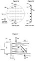
- FIG. 3 a is a top view of a wafer 180 being etched.
- the tilt axis runs along the diagonal of the wafer as shown with respect to the wafer top view.
- wafer 180 is being etched by an ion beam impinging on it from a direction perpendicular to the plane of the paper.
- FIG. 3 b is a cross section view of FIG. 3 a along the wafer diagonal perpendicular to the tilt axis.
- the wafer cross-section, direction of tilt axis runs along the middle of the wafer, and perpendicular to the plane of the paper.
- Asymmetry between the IB side 191 of the device and the OB side 192 of the device can be seen on the devices located towards the top and bottom of the wafer 180 .
- the asymmetry becomes more pronounced the further away the device is from the tilt axis, and as the tilt angle is increased, e.g., the wafer 180 is tilted further from the normal angle of incidence of the incident beam.
- ion sources generate an ion beam that is a collection of beamlets with a finite non-zero beam divergence, as illustrated in FIG. 4 .
- Beamlet divergence 131 is shown in this figure.
- a consequence of the beamlet divergence is that as the wafer is tilted away from normal beam incidence, there will be more intense etching on the side of the wafer 180 nearer to the ion source, and less intense etching on the side of the wafer 180 farther from the ion source.
- the etch depths can be made more uniform in the areas of the wafer 180 that are feature free.
- Devices on the wafers 180 however are typically made of features in 3-dimensions and not flat surfaces.
- the effect of the tilting of the wafer 180 away from normal beam incidence, in conjunction with beam divergence, is that the inboard side 191 of the devices on the wafer 180 will experience a different amount of beam exposure than the outboard side 192 of the devices.
- This inboard and outboard asymmetry becomes more pronounced as the location of the devices is farther away from the tilt axis of the wafer 180 , and as the tilt angle is increased away from normal beam incidence.
- Translating e.g., scanning
- the wafer 180 across the beam can address asymmetry between the inboard side 191 of the device and the outboard side 192 of the device.
- the region marked by double ended arrow 550 is the region where ion beam exposure of the wafer occurs.
- a single instance of translation of the wafer, translation starting at any point where all regions of the wafer is outside of the region shown by 550 , translation path taking the wafer through the region represented by 550 is considered one scan.
- region 550 where ion beam exposure occurs is defined through the introduction of physical beam blocks 171 , and 172 .
- the path of the wafer 180 during translation is defined as the scan path.
- the scan path can be within a plane that is parallel (or nearly parallel) to the plane of the tilted wafer surface for at least one scan.
- the scan path of wafer translation can be linear for at least one scan.
- the path of wafer translation can be non-linear (e.g., curved) for at least one scan.
- the scan path can be parallel to the tilted wafer 180 for at least one scan.
- the wafer tilt can be constant during the scan path for at least one scan.
- the wafer tilt can vary along the path of the scan for at least one scan.
- the scan path can be parallel to the wafer 180 during at least one point in the scan for at least one scan.
- the scan path can be parallel to the wafer 180 at all points during the scan for at least one scan.
- the scan path can be in a different plane than the wafer 180 for at least one scan.
- the scan path can be within a plane that is parallel (or nearly parallel) to the plane of the tilted wafer surface for all scans.
- the scan path of wafer translation can be linear for all scans.
- the path of wafer translation can be non-linear (e.g., curved) for all scans.
- the scan path can be parallel to the tilted wafer 180 for all scans.
- the wafer tilt can be constant during the scan path for all scans.
- the wafer tilt can vary along the path of the scan for all scans.
- the scan path can be parallel to the wafer 180 during at least one point in the scan for all scans.
- the scan path can be parallel to the wafer 180 at all points during the scan for all scans.
- the scan path can be in a different plane than the wafer 180 for all scans.
- the present disclosure relates to using asymmetric scanning velocity in an ion beam etch process to correct asymmetry of etching between the inboard side and the outboard side of device structures on a wafer while maintaining the overall uniformity of etch across the full wafer.
- the present disclosure relates to using asymmetric scanning velocity in an ion beam etch process to generate exaggerated asymmetry of etching between inboard and outboard sides of devices on a wafer, while maintaining the overall uniformity of etch across the full wafer.
- the present disclosure relates to using symmetric velocity scanning to enable control of inboard and outboard asymmetry even when the ion beam system is configured with a small ion source, and small grids.
- the ion source and grids will need to be of a lateral dimension larger than the sum of the wafer diameter, two times the beamlet divergence projected on the plane of the scan, and the ion beam density will need to be highly uniform across the lateral dimension.
- the present disclosure relates to using asymmetric velocity scans combined with symmetric velocity scans to address the inboard and outboard asymmetry and wafer etch uniformity, where the number of scans needed to finish the etch process may be a single scan or multiple scans.
- the present disclosure relates to a process whereby scan motion may be a straight linear motion of the wafer center across the ion beam or may include slight deviations from straight lines such as curved paths of motion of the wafer center across the ion beam.
- the present disclosure relates to an alternative to asymmetric velocity scan motion of the wafer where the ion beam current or the ion beam voltage is modulated as the wafer moves across the ion beam.
- the wafer may be exposed to either larger beam current or higher beam voltage when the wafer center is scanning on the far side of the scan beyond the mid-plane of the ion source.
- the present disclosure relates to an alternative to an asymmetric velocity profile scan by modulating the path of the scan, so that the wafer spends more time exposed to the ion beam on the far side of the scan after the wafer has passed the mid-plane of the ion source.
- the present disclosure relates to an alternative to the asymmetric velocity scan of the wafer across an ion beam by placing beam blocks in an asymmetric fashion with respect to the mid-plane of the ion source and grids, so that the wafer spends more time exposed to the ion beam on the far side of the scan even with the symmetrical velocity profile of the scan.
- a method of correcting asymmetry during a wafer etching process includes producing a plasma from a plasma source, the plasma source comprising a plasma chamber and an ion extraction grid system, the ion extraction grid system configured to produce an ion beam from the plasma, the ion beam having a central axis, supporting a wafer on a stage, scanning the wafer relative to the ion beam along a scan path, and modifying applied beam flux as a function of a position of the wafer.
- a method of correcting asymmetry during a wafer etching process includes producing a plasma from a plasma source, the plasma source comprising a plasma chamber and an ion extraction grid system, the ion extraction grid system configured to produce an ion beam from the plasma, the ion beam having a central axis, supporting a wafer on a stage including at least one of rotating the stage about the central axis and tilting the stage with respect to the ion beam during at least a portion of the etching process, scanning the wafer relative to the ion beam along a scan path in accordance with a scan velocity function, and modifying applied beam flux as a function of a position of the wafer by varying the scan velocity function as the wafer travels along the scan path.
- a method of correcting asymmetry during a wafer etching process includes producing a plasma from a plasma source, the plasma source comprising a plasma chamber and an ion extraction grid system, the ion extraction grid system configured to produce an ion beam from the plasma, the ion beam having a central axis, supporting a wafer on a stage, scanning the wafer relative to the ion beam along a scan path, the scan path comprising a scan out path from the first end of the ion beam to the second end of the ion beam according to a scan out velocity function and a scan back path from the second end of the ion beam to the first end of the ion beam according to a scan back velocity function, wherein one of the scan out velocity function and the scan back velocity function varies as a function of time, and modifying applied beam flux as a function of a position of the wafer.
- a method of correcting asymmetry during a wafer deposition process includes producing a plasma from a plasma source, the plasma source comprising a plasma chamber and an ion extraction grid system, the ion extraction grid system configured to produce an ion beam from the plasma, the ion beam having a central axis, supporting a wafer on a stage, scanning the wafer relative to the ion beam along a scan path, and modifying applied beam flux as a function of a position of the wafer.
- FIG. 1 illustrates an ion beam etch system
- FIG. 2 a illustrates symmetric etching
- FIG. 2 b illustrates asymmetric etching
- FIG. 2 c illustrates asymmetric etching
- FIG. 3 a is a top view of a wafer 180 being etched
- FIG. 3 b is a cross section view of FIG. 3 a along the wafer diagonal perpendicular to the tilt axis;
- FIG. 4 illustrates ion beam divergence
- FIG. 5 illustrates an improved scanning ion beam etch system according to an embodiment of the present disclosure
- FIG. 6 illustrates an improved scanning ion beam etch system according to an embodiment of the present disclosure
- FIG. 7 illustrates an improved scanning ion beam etch system according to an embodiment of the present disclosure
- FIG. 8 illustrates variable scan velocity according to an embodiment of the present disclosure
- FIG. 9 illustrates relative etch from the wafer center with constant scan velocity and variable scan velocity according to an embodiment of the present disclosure
- FIG. 10 a illustrates beamlet divergence and effect of divergence on the inboard side of the wafer versus the outboard side of wafer as the wafer is scanned across beam according to an embodiment of the present disclosure
- FIG. 10 b illustrates beamlet divergence and effect of divergence on the inboard side of the wafer versus the outboard side of wafer as the wafer is scanned across beam according to an embodiment of the present disclosure
- FIG. 11 a illustrates a beam that has a higher flux at the center of the beam
- FIG. 11 b illustrates a uniform beam where the flux is independent of position in the beam
- FIG. 12 illustrates the mid-plane of the source and far side of scan where preferential etching of the outboard side of devices occurs
- FIG. 13 illustrates one type of asymmetric velocity profile (solid lines) that preferentially etches the outboard side on the far side of the scan compared with a symmetric velocity (dashed lines) scan;
- FIG. 14 illustrates the mid-plane of the source, and near side of scan where preferential etching of the inboard side of the devices occurs.
- FIG. 15 illustrates one type of an asymmetric velocity profile that is a step type (solid lines) that preferentially etches the outboard side on the far side of the scan compared with an asymmetric velocity profile that is smoothly changing type (dashed lines) scan.
- FIG. 5 shows an illustration of an improved scanning ion beam etch (IBE) system of the present disclosure.
- Wafer 180 can be tilted off normal incidence with respect to the ion beam, and scanned across the beam starting from outside the beam on one end to the outside of the beam on the opposite end.
- IBE scanning ion beam etch
- the wafer scan velocity can be varied during a wafer scan.
- the wafer 180 is typically scanned back and forth in and/or through the beam 130 .
- a typical wafer scan can start with the wafer 180 in position 500 .
- the wafer 180 is scanned (e.g., translated) through the beam to position 510 .
- the wafer 180 can then be scanned (e.g., translated) back through the beam from position 510 to position 500 .
- the wafer 180 can be stopped (e.g., zero velocity) between scans (at either or both positions 500 and 510 ).
- the path from position 500 to position 510 and back again to position 500 can be a continuous path.
- the path the wafer 180 follows scanning from position 500 to position 510 can be the same as the path the wafer 180 follows scanning from position 510 to position 500 .
- the path the wafer 180 follows scanning from position 510 to 500 can be different from the path the wafer 180 follows scanning from position 500 to position 510 .
- the wafer 180 in position 500 and/or position 510 can be at least partially exposed to the beam.
- the wafer 180 in position 500 and/or position 510 can be completely exposed to the beam.
- the wafer 180 in position 500 and/or position 510 can be at least partially outside (e.g., not exposed to) the beam.
- the wafer 180 in position 500 and/or position 510 can be completely outside (e.g., not exposed to) the beam.
- the position of 500 and/or 510 can be invariant between at least two scans.
- the position 500 and/or 510 can be invariant for more than two scans.
- the position 500 and/or 510 can be invariant for all scans.
- the position of 500 and/or 510 can be changed between at least two scans.
- the position 500 and/or position 510 can be changed between more than two scans.
- the position 500 and/or position 510 can be changed between every scan.
- the length of the wafer scan (e.g., the distance between point 500 and 510 ) can be constant for at least 2 scans.
- the length of the wafer scan be constant for all scans.
- the length of the wafer scan can be different between at least 2 scans.
- the length of the wafer scan can be different in more than 2 scans.
- the length of the wafer scan can be different for all wafer scans.
- At least a portion of the wafer 180 can start the scan outside the ion beam. All of the wafer 180 can start the scan outside the ion beam. A portion of the wafer 180 can be exposed to the beam during a scan. All of the wafer 180 can be exposed to the beam during the scan. A portion of the wafer 180 can be outside the beam (e.g., not exposed to the beam) at the end of a scan. All of the wafer 180 can be outside of the beam (e.g., not exposed to the beam) at the end of a scan.
- the wafer 180 is not exposed to the beam at the start of a scan, a portion of the wafer 180 is exposed to the beam during the scan, and the wafer 180 is not exposed to the beam at the end of the scan.
- the wafer 180 can be scanned back and forth at a desired tilt angle with respect to the ion beam.
- the wafer 180 can be rotated about an axis 220 as it is scanned across the beam.
- the rotation speed can be constant during the scan.
- the rotation speed can vary during the scan.
- the process of scanning at fixed scan velocity can repeated until the desired etch depth is achieved.
- the scan path can be centered in the beam (e.g., the midpoint of the scan approximately coincides with the center of the beam).
- the scan path can be offset in the ion beam (e.g., the midpoint of the scan does not coincide with the center of the beam).
- This scanning method addresses the inboard and outboard asymmetry arising from the tilt of the wafer 180 and the divergence of the beamlets that cause the near side of the wafer 180 to be etched at a higher rate than the far side of the wafer 180 in a conventional ion beam etch (IBE) machine.
- IBE ion beam etch
- the wafer 180 can be tilted greater than approximately 10 degrees off normal incidence of the ion beam.
- the wafer 180 can be tilted greater than 30 degrees off normal incidence of the ion beam. Scanning at large tilt angles as shown in FIG. 6 , can result in the mid-point of the scan moving further away from the ion source, and the scan length increasing in order to be able to scan the wafer 180 across the ion beam. The increased scan length and the larger distance between the wafer 180 and the source can be difficult to accommodate in a High Vacuum/Ultra High Vacuum Chamber.
- the required scan length can be decreased by inserting physical blocks, 171 and 172 , towards the ends of the scan, as shown in FIG. 7 .
- the blocks 171 and 172 form an aperture that narrows the beam 130 , thus creating a portion or “slit” of the ion beam through which the wafer 180 is scanned.
- the blocks 171 and 172 may be inserted symmetrically with respect to the mid-plane 310 of the ion source 105 and ion extraction grid system 150 as shown in FIG. 7 .
- the blocks 171 and 172 can be inserted asymmetrically with respect to the mid-plane 310 .
- the slit width can be made adjustable by adjusting the positions of the upper block 171 , or the lower block 172 , or both. However, in cases where scanning the wafer 180 across the slit at large tilt angles is required, the distance from the ion extraction grid system 150 to the wafer 180 at its scan midpoint can be much larger than in conventional ion beam etch (IBE
- the beam density of beam 130 can be spatially non-uniform. This non-uniformity can be due to beamlet divergence. This effect often increases as the source-to-wafer distance increases and can be amplified by a large distance between the wafer scan's mid-point. Scanning the wafer 180 through the beam 130 at constant scan velocity can result in an etch that is highly non-uniform, with the wafer center etching much faster than the edge of the wafer. Deploying a variable scan velocity, as illustrated in the schematic in FIG. 8 , can dramatically improve the etch uniformity over the entire wafer 180 . Slowing down the velocity of the scan when the wafer 180 is away from the midpoint of the scan can enhance the etching at the points of the wafer 180 away from its center.
- the wafer velocity can be changed during the wafer scan.
- the wafer scan velocity can be continuously changing during a scan.
- the wafer scan velocity can be constant during some portion of a scan.
- the wafer velocity profile can be identical for at least 2 scans.
- the wafer scan velocity profile can be identical for all scans.
- the wafer scan velocity can change between at least two scans.
- the wafer scan velocity profile can change for each scan.
- the wafer scan velocity can be zero during at least one point during the scan.
- the wafer velocity profile can be symmetric (see FIG. 8 for example).
- the scan velocity profile can be monotonic.
- the scan velocity profile can be discontinuous.
- FIG. 8 Examples of symmetric variable velocity to achieve highly uniform etching over the full wafer 180 are shown in FIG. 8 .
- the direction of the scan is along the x-axis.
- the negative x-axis positions are closer to the ion source 105 than the positive x-axis positions.
- Variable velocity which is symmetric about the mid-point of the scan, is shown in the example in FIG. 8 .
- Symmetric variable velocity of the scan can be used to obtain uniform etching across the wafer 180 .
- the symmetric variable velocity profile can be a step function, or a smooth function, as shown in the example in FIG. 8 .
- Symmetric variable velocity as shown in the example here is used to obtain uniform etching across the full wafer 180 , as shown in FIG. 9 .
- Scanning the wafer 180 across the beam 130 does not address a second cause of inboard and outboard asymmetry of devices.
- This second cause of asymmetry is caused by the large distance needed to enable the scanning of a tilted wafer 180 across the beam 130 , the finite size of the ion source 105 and ion extraction grid system 150 , and the beamlet divergence. This effect is illustrated in FIGS. 10 a -10 b .
- the finite lateral size of the ion source 105 , and the beamlet divergences cause the inboard side 191 of the devices to be exposed to larger amount of ions compared to the outboard side of the device. This asymmetry is present at all tilt angles. This is illustrated in FIGS.
- a rotating wafer 180 causes the outboard side 192 of the device, at the outer edges of the wafer 180 , to etch much less than the inboard side 191 of the device as seen in FIGS. 10 a -10 b .
- Solid angles projected from the inboard side 191 of the device and the outboard side 192 of the device, to the plane of the ion extraction grid system 150 represent the amount of beam exposure on the inboard side 191 , and outboard side 192 respectively, as the wafer 180 is scanned across the beam 130 .
- the imbalance of the beam exposure of the inboard side 191 and outboard side 192 of the devices can be clearly seen in FIG. 10 a and FIG. 10 b.
- FIGS. 11 a -11 b show a beam 130 that has a higher flux at the center of the beam 130 . It is possible to have a beam 130 that has a higher flux at the edge of the beam 130 than at the center of the beam 130 (not shown).
- FIG. 11 b shows a uniform beam 130 where the flux is independent of the position in the beam 130 .
- the Y-axis direction is the direction of a scan.
- Increasing the lateral dimension of the ion source 105 and grids of the ion extraction grid system 150 to be at least equal to the sum of wafer diameter and twice the beamlet divergence and making the ion flux uniform across the lateral dimension, as shown in FIG. 11 b , can allow both the inboard side 191 and outboard side 192 of the devices to be exposed to the same amount of ion beam exposure, and eliminate the asymmetry between the inboard side 191 and outboard side 192 of the devices.
- the non-ideal ion beam shown in FIG. 11 a shows an example of when the flux of the ion beam 130 is higher in the center of the beam 130 compared to an edge of the beam 130 . It is possible to have an ion beam 130 where the flux of the ion beam 130 is higher at an edge of the beam 130 compared to the center of the beam 130 (e.g., through magnetic confinement of the beam, a non-uniform grid system, etc.). In this case, it may be desirable to increase the dose in the center of the wafer 180 compared to the edge of the wafer 180 during a scan.
- the scan velocity at an end of a scan can be greater than the scan velocity in the center of the scan (e.g., the scan velocity for at least one point towards the end of the scan is higher than a point toward the center of the scan).
- slowing down the scan velocity when the wafer center is on the far side of the scan 301 can also improve uniformity.
- the scan velocity can be reduced for at least a portion of points below the mid-plane 310 of the ion source 105 and ion extraction grid system 150 .
- the reduced scan speed enhances the etching on the outboard side 192 of the devices.
- FIG. 13 shows an example of a scan velocity profile described by the system of the present disclosure.
- the positive x positions are the far side positions 301 of the wafer center where the scan speed is reduced to increase the etching on the outboard side 192 of the device.
- Overall excellent uniformity of etching across the full wafer 180 is preserved by increasing the scan velocity on the negative X side of the scan (e.g., when the wafer 180 is closer to the ion source 105 ), than what a symmetric variable scan profile 303 requires for good uniformity.
- a scan velocity can be a function of the wafer distance from the ion beam 105 during a scan.
- a scan velocity can decrease as the distance between the wafer 180 and the ion beam 130 increases during a scan.
- a scan velocity can increase as the area of the wafer 180 exposed to the beam 130 increases.
- a scan velocity can decrease as the area of the wafer 180 exposed to the beam 130 decreases.
- a scan acceleration can vary during a scan.
- a scan acceleration profile can be asymmetric.
- a scan acceleration can be identical between at least 2 scans.
- a scan acceleration curve is a plot of the wafer acceleration vs. the position of the wafer 180 along the scan path.
- a scan acceleration curve can be identical for more than 2 scans.
- a scan acceleration curve can be identical for all scans.
- a scan acceleration curve can be different between at least 2 scans.
- a scan acceleration curve can be different for more than 2 scans.
- a scan acceleration curve can be different for all scans.
- a scan acceleration can be constant during at least a portion of a scan.
- a scan velocity can be selected to maintain a constant dose of ions across at least one region of the wafer 180 during a scan.
- a scan velocity can be selected to maintain a constant dose of ions across all exposed regions of the wafer 180 during a scan.
- the shape of the velocity versus position can be a stepped velocity configuration or a smoothly varied configuration, represented by 304 in FIG. 15 .
- An asymmetrical velocity profile causes the wafer 180 to spend more time on the positive x-side (e.g., further away from the ion source 105 ) than on the negative x-side, assuring more etching on the outboard side 192 of devices compared to the inboard side 191 of the devices.
- This process of asymmetric velocity of the scan enables inboard and outboard asymmetry control even when the etching system is configured with an ion source 105 having lateral dimensions smaller than the sum of wafer diameter and twice the beamlet divergence projection on the wafer scan plane.
- the inboard side 191 of the device can be preferentially etched by slowing down the scan speed on the near side to correct for asymmetry arising in systems with sources that have a beam of less density at the center of the source compared to the density away from the center of the source.
- Exemplary ion beam etch process parameters are as follows.
Landscapes
- Engineering & Computer Science (AREA)
- Physics & Mathematics (AREA)
- Chemical & Material Sciences (AREA)
- Analytical Chemistry (AREA)
- Plasma & Fusion (AREA)
- General Physics & Mathematics (AREA)
- Condensed Matter Physics & Semiconductors (AREA)
- Manufacturing & Machinery (AREA)
- Computer Hardware Design (AREA)
- Microelectronics & Electronic Packaging (AREA)
- Power Engineering (AREA)
- Drying Of Semiconductors (AREA)
- Plasma Technology (AREA)
- Weting (AREA)
Abstract
Description
-
- Plasma source power approximately in the range of 100 W-5 kW.
- Process chamber pressures in the range of 1E-3 Torr to 1E-5 Torr.
- Gas compositions can contain an inert gas (e.g., Ar, Kr, Xe, He, etc., or mixtures of these).
- Gas compositions can contain reactive gases (e.g., halogen containing gases, CxHyFz, Cl2, oxygen containing gases, O2, nitrogen containing gases, N2, NF3, carbon containing gases, CH4, CO, CO2, sulfur containing gases, SF6, hydrogen containing gases, H2, H2O, or mixtures of these).
- Gas compositions can contain a mixture of inert and reactive gases.
- Wafer temperature can range from approximately −40 C to 400 C.
- Wafer scan speeds can range from approximately 0.01 mm/sec to 1 cm/sec. In one embodiment, the wafer scan speeds range from 1 mm/sec to 100 mm/sec.
- Wafer rotation speeds range from approximately 0.5 RPM to 1000 RPM.
- Ion beam voltages are typically less than about 500 eV.
- Wafer tilt angles range from approximately 1 degree (e.g., 1 degree off perpendicular to the ion beam 105) to about 85 degrees (e.g., a glancing angle to the ion beam 105).
Claims (60)
Priority Applications (8)
| Application Number | Priority Date | Filing Date | Title |
|---|---|---|---|
| US16/398,487 US11227741B2 (en) | 2018-05-03 | 2019-04-30 | Scanning ion beam etch |
| EP19724655.6A EP3788646A2 (en) | 2018-05-03 | 2019-05-01 | Scanning ion beam etch |
| PCT/US2019/030255 WO2019213301A2 (en) | 2018-05-03 | 2019-05-01 | Scanning ion beam etch |
| JP2020561022A JP7097990B2 (en) | 2018-05-03 | 2019-05-01 | Scanning ion beam etching |
| CN201980027056.7A CN112041964A (en) | 2018-05-03 | 2019-05-01 | Scanning ion beam etching |
| KR1020207030496A KR102478522B1 (en) | 2018-05-03 | 2019-05-01 | Scanning ion beam etching |
| US17/536,025 US11646171B2 (en) | 2018-05-03 | 2021-11-27 | Scanning ion beam etch |
| US17/686,356 US20220189727A1 (en) | 2018-05-03 | 2022-03-03 | Scanning ion beam deposition and etch |
Applications Claiming Priority (2)
| Application Number | Priority Date | Filing Date | Title |
|---|---|---|---|
| US201862666324P | 2018-05-03 | 2018-05-03 | |
| US16/398,487 US11227741B2 (en) | 2018-05-03 | 2019-04-30 | Scanning ion beam etch |
Related Child Applications (2)
| Application Number | Title | Priority Date | Filing Date |
|---|---|---|---|
| US17/536,025 Division US11646171B2 (en) | 2018-05-03 | 2021-11-27 | Scanning ion beam etch |
| US17/536,025 Continuation US11646171B2 (en) | 2018-05-03 | 2021-11-27 | Scanning ion beam etch |
Publications (2)
| Publication Number | Publication Date |
|---|---|
| US20190341221A1 US20190341221A1 (en) | 2019-11-07 |
| US11227741B2 true US11227741B2 (en) | 2022-01-18 |
Family
ID=68385176
Family Applications (2)
| Application Number | Title | Priority Date | Filing Date |
|---|---|---|---|
| US16/398,487 Active US11227741B2 (en) | 2018-05-03 | 2019-04-30 | Scanning ion beam etch |
| US17/536,025 Active US11646171B2 (en) | 2018-05-03 | 2021-11-27 | Scanning ion beam etch |
Family Applications After (1)
| Application Number | Title | Priority Date | Filing Date |
|---|---|---|---|
| US17/536,025 Active US11646171B2 (en) | 2018-05-03 | 2021-11-27 | Scanning ion beam etch |
Country Status (7)
| Country | Link |
|---|---|
| US (2) | US11227741B2 (en) |
| EP (1) | EP3788646A2 (en) |
| JP (1) | JP7097990B2 (en) |
| KR (1) | KR102478522B1 (en) |
| CN (1) | CN112041964A (en) |
| TW (1) | TWI776053B (en) |
| WO (1) | WO2019213301A2 (en) |
Cited By (2)
| Publication number | Priority date | Publication date | Assignee | Title |
|---|---|---|---|---|
| US20220084779A1 (en) * | 2018-05-03 | 2022-03-17 | Plasma-Therm Nes Llc | Scanning Ion Beam Etch |
| WO2023167774A1 (en) * | 2022-03-03 | 2023-09-07 | Plasma-Therm Nes, Llc | Scanning ion beam deposition and etch |
Citations (25)
| Publication number | Priority date | Publication date | Assignee | Title |
|---|---|---|---|---|
| US4278493A (en) | 1980-04-28 | 1981-07-14 | International Business Machines Corporation | Method for cleaning surfaces by ion milling |
| US6677599B2 (en) | 2000-03-27 | 2004-01-13 | Applied Materials, Inc. | System and method for uniformly implanting a wafer with an ion beam |
| US20050214477A1 (en) | 2004-03-26 | 2005-09-29 | Applied Materials, Inc. | Chemical vapor deposition plasma process using an ion shower grid |
| US7166854B2 (en) | 2003-12-09 | 2007-01-23 | Varian Semiconductor Equipment Associates, Inc. | Uniformity control multiple tilt axes, rotating wafer and variable scan velocity |
| US7176470B1 (en) | 2005-12-22 | 2007-02-13 | Varian Semiconductor Equipment Associates, Inc. | Technique for high-efficiency ion implantation |
| CN101399147A (en) | 2007-09-27 | 2009-04-01 | 汉辰科技股份有限公司 | Ion implantation method |
| US20090084757A1 (en) | 2007-09-28 | 2009-04-02 | Yuri Erokhin | Uniformity control for ion beam assisted etching |
| WO2009045722A1 (en) | 2007-09-28 | 2009-04-09 | Varian Semiconductor Equipment Associates, Inc. | Two-diemensional uniformity correction for ion beam assisted etching |
| US7561983B2 (en) | 2006-09-29 | 2009-07-14 | Varian Semiconductor Equipment Associates, Inc. | Technique for improving ion implantation based on ion beam angle-related information |
| JP2009246009A (en) | 2008-03-28 | 2009-10-22 | Seiko Epson Corp | Vacuum processing apparatus and vacuum processing method |
| KR100954484B1 (en) | 2007-07-26 | 2010-04-22 | 어드밴스드 이온 빔 테크놀로지 인크. | Ion Implantation Method |
| CN102290341A (en) | 2007-09-27 | 2011-12-21 | 汉辰科技股份有限公司 | Ion implantation method |
| CN102324383A (en) | 2007-09-27 | 2012-01-18 | 汉辰科技股份有限公司 | Ion implantation method |
| US20140227460A1 (en) | 2013-02-12 | 2014-08-14 | Hariharakeshava Sarpangala Hegde | Methods for addressing inboard-outboard asymmetry in substrate processing |
| US20150090583A1 (en) | 2012-06-29 | 2015-04-02 | Canon Anelva Corporation | Ion beam processing method and ion beam processing apparatus |
| US20160064232A1 (en) | 2014-08-29 | 2016-03-03 | Lam Research Corporation | Ion beam etch without need for wafer tilt or rotation |
| US20160155602A1 (en) | 2013-07-29 | 2016-06-02 | Hitachi High-Technologies Corporation | Ion Milling Device and Processing Method Using the Ion Milling Device |
| CN105957790A (en) | 2016-07-01 | 2016-09-21 | 苏州至臻精密光学有限公司 | Ion beam etching machine and etching method thereof |
| US20170069526A1 (en) | 2015-09-03 | 2017-03-09 | Jongsoon Park | Chuck assembly with tiltable chuck and semiconductor fabrication system including the same |
| US20180068828A1 (en) * | 2016-09-07 | 2018-03-08 | Axcelis Technologies, Inc. | In situ beam current monitoring and control in scanned ion implantation systems |
| US9966092B2 (en) | 2015-10-02 | 2018-05-08 | Canon Anelva Corporation | Ion beam etching method and ion beam etching apparatus |
| US20180154443A1 (en) * | 2016-12-06 | 2018-06-07 | Velo3D, Inc. | Optics, detectors, and three-dimensional printing |
| US20180158643A1 (en) | 2016-12-06 | 2018-06-07 | Jongchul PARK | Ion beam apparatus including slit structure for extracting ion beam, etching method using the same, and method for manufacturing magnetic memory device using the ion beam apparatus |
| US20180197715A1 (en) * | 2017-01-09 | 2018-07-12 | Tel Epion Inc. | Compensated location specific processing apparatus and method |
| US20190148109A1 (en) * | 2017-11-10 | 2019-05-16 | Lam Research Corporation | Method and Apparatus for Anisotropic Pattern Etching and Treatment |
Family Cites Families (10)
| Publication number | Priority date | Publication date | Assignee | Title |
|---|---|---|---|---|
| JPH0412446A (en) * | 1990-04-27 | 1992-01-17 | Sumitomo Electric Ind Ltd | Ion beam radiating device |
| JPH08134668A (en) * | 1994-11-02 | 1996-05-28 | Hitachi Ltd | Ion beam milling method and device therefor |
| JP3297736B2 (en) | 1999-12-16 | 2002-07-02 | 東京大学長 | Method and apparatus for analyzing element distribution in the depth direction using precision section processing by focused ion beam |
| TW539845B (en) * | 2000-07-27 | 2003-07-01 | Ebara Corp | Sheet beam-type inspection device |
| JP4253553B2 (en) | 2003-09-29 | 2009-04-15 | 株式会社日立ハイテクノロジーズ | Method of forming film using charged particle beam, selective etching method, and charged particle beam apparatus |
| KR101687565B1 (en) * | 2009-03-30 | 2016-12-19 | 도쿄엘렉트론가부시키가이샤 | Plasma processing apparatus and plasma processing method |
| US9455116B2 (en) * | 2014-04-30 | 2016-09-27 | Axcells Technologies, Inc. | Angular scanning using angular energy filter |
| WO2016093087A1 (en) | 2014-12-09 | 2016-06-16 | 東京エレクトロン株式会社 | Pattern forming method, gas cluster ion beam irradiation system and pattern forming apparatus |
| JP2016207925A (en) * | 2015-04-27 | 2016-12-08 | 株式会社アドバンテスト | Element, manufacturing method and exposure device |
| US11227741B2 (en) * | 2018-05-03 | 2022-01-18 | Plasma-Therm Nes Llc | Scanning ion beam etch |
-
2019
- 2019-04-30 US US16/398,487 patent/US11227741B2/en active Active
- 2019-05-01 EP EP19724655.6A patent/EP3788646A2/en not_active Withdrawn
- 2019-05-01 CN CN201980027056.7A patent/CN112041964A/en active Pending
- 2019-05-01 WO PCT/US2019/030255 patent/WO2019213301A2/en active Application Filing
- 2019-05-01 JP JP2020561022A patent/JP7097990B2/en active Active
- 2019-05-01 KR KR1020207030496A patent/KR102478522B1/en active IP Right Grant
- 2019-05-02 TW TW108115235A patent/TWI776053B/en active
-
2021
- 2021-11-27 US US17/536,025 patent/US11646171B2/en active Active
Patent Citations (25)
| Publication number | Priority date | Publication date | Assignee | Title |
|---|---|---|---|---|
| US4278493A (en) | 1980-04-28 | 1981-07-14 | International Business Machines Corporation | Method for cleaning surfaces by ion milling |
| US6677599B2 (en) | 2000-03-27 | 2004-01-13 | Applied Materials, Inc. | System and method for uniformly implanting a wafer with an ion beam |
| US7166854B2 (en) | 2003-12-09 | 2007-01-23 | Varian Semiconductor Equipment Associates, Inc. | Uniformity control multiple tilt axes, rotating wafer and variable scan velocity |
| US20050214477A1 (en) | 2004-03-26 | 2005-09-29 | Applied Materials, Inc. | Chemical vapor deposition plasma process using an ion shower grid |
| US7176470B1 (en) | 2005-12-22 | 2007-02-13 | Varian Semiconductor Equipment Associates, Inc. | Technique for high-efficiency ion implantation |
| US7561983B2 (en) | 2006-09-29 | 2009-07-14 | Varian Semiconductor Equipment Associates, Inc. | Technique for improving ion implantation based on ion beam angle-related information |
| KR100954484B1 (en) | 2007-07-26 | 2010-04-22 | 어드밴스드 이온 빔 테크놀로지 인크. | Ion Implantation Method |
| CN101399147A (en) | 2007-09-27 | 2009-04-01 | 汉辰科技股份有限公司 | Ion implantation method |
| CN102324383A (en) | 2007-09-27 | 2012-01-18 | 汉辰科技股份有限公司 | Ion implantation method |
| CN102290341A (en) | 2007-09-27 | 2011-12-21 | 汉辰科技股份有限公司 | Ion implantation method |
| US20090084757A1 (en) | 2007-09-28 | 2009-04-02 | Yuri Erokhin | Uniformity control for ion beam assisted etching |
| WO2009045722A1 (en) | 2007-09-28 | 2009-04-09 | Varian Semiconductor Equipment Associates, Inc. | Two-diemensional uniformity correction for ion beam assisted etching |
| JP2009246009A (en) | 2008-03-28 | 2009-10-22 | Seiko Epson Corp | Vacuum processing apparatus and vacuum processing method |
| US20150090583A1 (en) | 2012-06-29 | 2015-04-02 | Canon Anelva Corporation | Ion beam processing method and ion beam processing apparatus |
| US20140227460A1 (en) | 2013-02-12 | 2014-08-14 | Hariharakeshava Sarpangala Hegde | Methods for addressing inboard-outboard asymmetry in substrate processing |
| US20160155602A1 (en) | 2013-07-29 | 2016-06-02 | Hitachi High-Technologies Corporation | Ion Milling Device and Processing Method Using the Ion Milling Device |
| US20160064232A1 (en) | 2014-08-29 | 2016-03-03 | Lam Research Corporation | Ion beam etch without need for wafer tilt or rotation |
| US20170069526A1 (en) | 2015-09-03 | 2017-03-09 | Jongsoon Park | Chuck assembly with tiltable chuck and semiconductor fabrication system including the same |
| US9966092B2 (en) | 2015-10-02 | 2018-05-08 | Canon Anelva Corporation | Ion beam etching method and ion beam etching apparatus |
| CN105957790A (en) | 2016-07-01 | 2016-09-21 | 苏州至臻精密光学有限公司 | Ion beam etching machine and etching method thereof |
| US20180068828A1 (en) * | 2016-09-07 | 2018-03-08 | Axcelis Technologies, Inc. | In situ beam current monitoring and control in scanned ion implantation systems |
| US20180154443A1 (en) * | 2016-12-06 | 2018-06-07 | Velo3D, Inc. | Optics, detectors, and three-dimensional printing |
| US20180158643A1 (en) | 2016-12-06 | 2018-06-07 | Jongchul PARK | Ion beam apparatus including slit structure for extracting ion beam, etching method using the same, and method for manufacturing magnetic memory device using the ion beam apparatus |
| US20180197715A1 (en) * | 2017-01-09 | 2018-07-12 | Tel Epion Inc. | Compensated location specific processing apparatus and method |
| US20190148109A1 (en) * | 2017-11-10 | 2019-05-16 | Lam Research Corporation | Method and Apparatus for Anisotropic Pattern Etching and Treatment |
Non-Patent Citations (5)
| Title |
|---|
| "Quick guide on laser beam divergence measurement" via https://www.gentec-eo.com/blog/laser-beam-divergence-measurement; pp. 1-7 (Year: 2018). * |
| "Silicon Wafer and its Different Diameters" via https://www.waferworld.com/silicon-wafer-different-diameters/; pp. 1-4 (Year: 2019). * |
| Goglia Peter et al., Advanced Techniques for Enhanced Ion Beam Etch Uniformity, 2018 China Semiconductor Technology International Conference (CSTIC) Mar. 11-12, 2018, IEEE, May 31, 2018, pp. 1-3, XP033351657, DOI: 10.1109/CSTIC.2018.8369232, Abstract, pp. 1-3; Figures 1-3, 5, 7, 8. |
| GOGLIA PETER; HEGDE HARI; PILLOUX YANNICK: "Advanced techniques for enhanced Ion Beam Etch uniformity", 2018 CHINA SEMICONDUCTOR TECHNOLOGY INTERNATIONAL CONFERENCE (CSTIC), IEEE, 11 March 2018 (2018-03-11), pages 1 - 3, XP033351657, DOI: 10.1109/CSTIC.2018.8369232 |
| RP Photonics Encyclopedia, "Beam Divergence" via https://www.rp-photonics.com/beam_divergence.html ; pp. 1-7 (Year: 2020). * |
Cited By (3)
| Publication number | Priority date | Publication date | Assignee | Title |
|---|---|---|---|---|
| US20220084779A1 (en) * | 2018-05-03 | 2022-03-17 | Plasma-Therm Nes Llc | Scanning Ion Beam Etch |
| US11646171B2 (en) * | 2018-05-03 | 2023-05-09 | Plasma-Therm Nes Llc | Scanning ion beam etch |
| WO2023167774A1 (en) * | 2022-03-03 | 2023-09-07 | Plasma-Therm Nes, Llc | Scanning ion beam deposition and etch |
Also Published As
| Publication number | Publication date |
|---|---|
| WO2019213301A2 (en) | 2019-11-07 |
| JP2021522689A (en) | 2021-08-30 |
| WO2019213301A3 (en) | 2019-12-26 |
| TW201947630A (en) | 2019-12-16 |
| CN112041964A (en) | 2020-12-04 |
| KR102478522B1 (en) | 2022-12-20 |
| US20190341221A1 (en) | 2019-11-07 |
| EP3788646A2 (en) | 2021-03-10 |
| TWI776053B (en) | 2022-09-01 |
| US11646171B2 (en) | 2023-05-09 |
| US20220084779A1 (en) | 2022-03-17 |
| JP7097990B2 (en) | 2022-07-08 |
| KR20210006886A (en) | 2021-01-19 |
Similar Documents
| Publication | Publication Date | Title |
|---|---|---|
| US11646171B2 (en) | Scanning ion beam etch | |
| TWI455185B (en) | Systems and methods for beam angle adjustment in ion implanters | |
| US9514912B2 (en) | Control of ion angular distribution of ion beams with hidden deflection electrode | |
| JP7254791B2 (en) | Method and apparatus for anisotropic pattern etching and processing | |
| US9142386B2 (en) | Ion beam line | |
| KR101900334B1 (en) | Ion beam etching method and ion beam etching apparatus | |
| US11195703B2 (en) | Apparatus and techniques for angled etching using multielectrode extraction source | |
| US20140124363A1 (en) | Ion beam generator and ion beam plasma processing apparatus | |
| US20220189727A1 (en) | Scanning ion beam deposition and etch | |
| CN211507564U (en) | Electrode for electrostatic filter | |
| JP6428726B2 (en) | Ion implantation system | |
| WO2023167774A1 (en) | Scanning ion beam deposition and etch | |
| US9697988B2 (en) | Ion implantation system and process | |
| JP7280983B2 (en) | Ion milling device | |
| US9748072B2 (en) | Lower dose rate ion implantation using a wider ion beam | |
| US11270864B2 (en) | Apparatus and system including extraction optics having movable blockers | |
| US20170077001A1 (en) | Method for high throughput using beam scan size and beam position in beam processing system |
Legal Events
| Date | Code | Title | Description |
|---|---|---|---|
| FEPP | Fee payment procedure |
Free format text: ENTITY STATUS SET TO UNDISCOUNTED (ORIGINAL EVENT CODE: BIG.); ENTITY STATUS OF PATENT OWNER: SMALL ENTITY |
|
| FEPP | Fee payment procedure |
Free format text: ENTITY STATUS SET TO SMALL (ORIGINAL EVENT CODE: SMAL); ENTITY STATUS OF PATENT OWNER: SMALL ENTITY |
|
| AS | Assignment |
Owner name: PLASMA-THERM NES LLC, FLORIDA Free format text: ASSIGNMENT OF ASSIGNORS INTEREST;ASSIGNORS:HEGDE, SARPANGALA H.;LEE, VINCENT;REEL/FRAME:049434/0189 Effective date: 20190501 |
|
| STPP | Information on status: patent application and granting procedure in general |
Free format text: DOCKETED NEW CASE - READY FOR EXAMINATION |
|
| STPP | Information on status: patent application and granting procedure in general |
Free format text: NON FINAL ACTION MAILED |
|
| STPP | Information on status: patent application and granting procedure in general |
Free format text: NON FINAL ACTION MAILED |
|
| STPP | Information on status: patent application and granting procedure in general |
Free format text: RESPONSE TO NON-FINAL OFFICE ACTION ENTERED AND FORWARDED TO EXAMINER |
|
| STPP | Information on status: patent application and granting procedure in general |
Free format text: FINAL REJECTION MAILED |
|
| STPP | Information on status: patent application and granting procedure in general |
Free format text: DOCKETED NEW CASE - READY FOR EXAMINATION |
|
| STPP | Information on status: patent application and granting procedure in general |
Free format text: NOTICE OF ALLOWANCE MAILED -- APPLICATION RECEIVED IN OFFICE OF PUBLICATIONS |
|
| STPP | Information on status: patent application and granting procedure in general |
Free format text: PUBLICATIONS -- ISSUE FEE PAYMENT VERIFIED |
|
| STCF | Information on status: patent grant |
Free format text: PATENTED CASE |
|
| AS | Assignment |
Owner name: VALLEY NATIONAL BANK, FLORIDA Free format text: SECURITY INTEREST;ASSIGNORS:RAJE TECHNOLOGY GROUP, LLC;PLASMA-THERM, LLC;REV-TECH MANUFACTURING SOLUTIONS, LLC;AND OTHERS;REEL/FRAME:060447/0766 Effective date: 20220602 |