US11222920B2 - Magnetic device including multiferroic regions and methods of forming the same - Google Patents
Magnetic device including multiferroic regions and methods of forming the same Download PDFInfo
- Publication number
- US11222920B2 US11222920B2 US16/781,225 US202016781225A US11222920B2 US 11222920 B2 US11222920 B2 US 11222920B2 US 202016781225 A US202016781225 A US 202016781225A US 11222920 B2 US11222920 B2 US 11222920B2
- Authority
- US
- United States
- Prior art keywords
- portions
- magnetic
- layer
- multiferroic
- electrode
- Prior art date
- Legal status (The legal status is an assumption and is not a legal conclusion. Google has not performed a legal analysis and makes no representation as to the accuracy of the status listed.)
- Active, expires
Links
- 230000005291 magnetic effect Effects 0.000 title claims abstract description 243
- 238000000034 method Methods 0.000 title claims description 22
- 230000007847 structural defect Effects 0.000 claims abstract description 65
- 230000005294 ferromagnetic effect Effects 0.000 claims abstract description 42
- 230000005415 magnetization Effects 0.000 claims description 62
- 238000010884 ion-beam technique Methods 0.000 claims description 42
- 239000000463 material Substances 0.000 claims description 28
- 230000004888 barrier function Effects 0.000 claims description 25
- 230000010287 polarization Effects 0.000 claims description 25
- 230000008878 coupling Effects 0.000 claims description 14
- 238000010168 coupling process Methods 0.000 claims description 14
- 238000005859 coupling reaction Methods 0.000 claims description 14
- SWQJXJOGLNCZEY-UHFFFAOYSA-N helium atom Chemical group [He] SWQJXJOGLNCZEY-UHFFFAOYSA-N 0.000 claims description 13
- GYHNNYVSQQEPJS-UHFFFAOYSA-N Gallium Chemical compound [Ga] GYHNNYVSQQEPJS-UHFFFAOYSA-N 0.000 claims description 12
- 229910052733 gallium Inorganic materials 0.000 claims description 11
- 239000013078 crystal Substances 0.000 claims description 9
- 230000008569 process Effects 0.000 claims description 9
- 230000000946 synaptic effect Effects 0.000 claims description 9
- 229910002902 BiFeO3 Inorganic materials 0.000 claims description 6
- 229910021632 Barium Tetrafluoronickelate Inorganic materials 0.000 claims description 3
- 229910009567 YMnO3 Inorganic materials 0.000 claims description 3
- 239000010410 layer Substances 0.000 description 319
- 150000002500 ions Chemical class 0.000 description 14
- 230000005290 antiferromagnetic effect Effects 0.000 description 13
- 230000008859 change Effects 0.000 description 13
- 230000005684 electric field Effects 0.000 description 11
- 230000006870 function Effects 0.000 description 11
- 239000007769 metal material Substances 0.000 description 9
- 230000015572 biosynthetic process Effects 0.000 description 8
- 229910052734 helium Inorganic materials 0.000 description 7
- 239000001307 helium Substances 0.000 description 7
- 239000011810 insulating material Substances 0.000 description 7
- 229910052715 tantalum Inorganic materials 0.000 description 7
- KJTLSVCANCCWHF-UHFFFAOYSA-N Ruthenium Chemical compound [Ru] KJTLSVCANCCWHF-UHFFFAOYSA-N 0.000 description 5
- 229910052802 copper Inorganic materials 0.000 description 5
- 239000010949 copper Substances 0.000 description 5
- 239000003302 ferromagnetic material Substances 0.000 description 5
- CPLXHLVBOLITMK-UHFFFAOYSA-N magnesium oxide Inorganic materials [Mg]=O CPLXHLVBOLITMK-UHFFFAOYSA-N 0.000 description 5
- 229910052751 metal Inorganic materials 0.000 description 5
- 239000002184 metal Substances 0.000 description 5
- 239000000203 mixture Substances 0.000 description 5
- 229910052707 ruthenium Inorganic materials 0.000 description 5
- 230000005621 ferroelectricity Effects 0.000 description 4
- 239000000395 magnesium oxide Substances 0.000 description 4
- 239000000758 substrate Substances 0.000 description 4
- GUVRBAGPIYLISA-UHFFFAOYSA-N tantalum atom Chemical compound [Ta] GUVRBAGPIYLISA-UHFFFAOYSA-N 0.000 description 4
- 229910052721 tungsten Inorganic materials 0.000 description 4
- ATJFFYVFTNAWJD-UHFFFAOYSA-N Tin Chemical compound [Sn] ATJFFYVFTNAWJD-UHFFFAOYSA-N 0.000 description 3
- -1 copper nitride Chemical class 0.000 description 3
- 230000007547 defect Effects 0.000 description 3
- 239000003989 dielectric material Substances 0.000 description 3
- 238000006073 displacement reaction Methods 0.000 description 3
- 239000001995 intermetallic alloy Substances 0.000 description 3
- 238000010849 ion bombardment Methods 0.000 description 3
- AXZKOIWUVFPNLO-UHFFFAOYSA-N magnesium;oxygen(2-) Chemical compound [O-2].[Mg+2] AXZKOIWUVFPNLO-UHFFFAOYSA-N 0.000 description 3
- 150000004767 nitrides Chemical class 0.000 description 3
- 229920002120 photoresistant polymer Polymers 0.000 description 3
- 239000004065 semiconductor Substances 0.000 description 3
- 229910052719 titanium Inorganic materials 0.000 description 3
- 229910019236 CoFeB Inorganic materials 0.000 description 2
- 239000004020 conductor Substances 0.000 description 2
- 239000000109 continuous material Substances 0.000 description 2
- 239000002178 crystalline material Substances 0.000 description 2
- 238000010586 diagram Methods 0.000 description 2
- 239000011521 glass Substances 0.000 description 2
- 238000002955 isolation Methods 0.000 description 2
- 238000012986 modification Methods 0.000 description 2
- 230000004048 modification Effects 0.000 description 2
- 238000000059 patterning Methods 0.000 description 2
- 239000005368 silicate glass Substances 0.000 description 2
- 230000005641 tunneling Effects 0.000 description 2
- 229910003321 CoFe Inorganic materials 0.000 description 1
- RYGMFSIKBFXOCR-UHFFFAOYSA-N Copper Chemical compound [Cu] RYGMFSIKBFXOCR-UHFFFAOYSA-N 0.000 description 1
- 229910052581 Si3N4 Inorganic materials 0.000 description 1
- VYPSYNLAJGMNEJ-UHFFFAOYSA-N Silicium dioxide Chemical compound O=[Si]=O VYPSYNLAJGMNEJ-UHFFFAOYSA-N 0.000 description 1
- 230000005303 antiferromagnetism Effects 0.000 description 1
- 238000000231 atomic layer deposition Methods 0.000 description 1
- 239000000919 ceramic Substances 0.000 description 1
- 238000005229 chemical vapour deposition Methods 0.000 description 1
- 238000000151 deposition Methods 0.000 description 1
- 230000000694 effects Effects 0.000 description 1
- 230000005308 ferrimagnetism Effects 0.000 description 1
- 230000005307 ferromagnetism Effects 0.000 description 1
- 230000005669 field effect Effects 0.000 description 1
- 238000002513 implantation Methods 0.000 description 1
- 239000011159 matrix material Substances 0.000 description 1
- 229910044991 metal oxide Inorganic materials 0.000 description 1
- 150000004706 metal oxides Chemical class 0.000 description 1
- TWNQGVIAIRXVLR-UHFFFAOYSA-N oxo(oxoalumanyloxy)alumane Chemical compound O=[Al]O[Al]=O TWNQGVIAIRXVLR-UHFFFAOYSA-N 0.000 description 1
- 238000005240 physical vapour deposition Methods 0.000 description 1
- 238000004549 pulsed laser deposition Methods 0.000 description 1
- HQVNEWCFYHHQES-UHFFFAOYSA-N silicon nitride Chemical compound N12[Si]34N5[Si]62N3[Si]51N64 HQVNEWCFYHHQES-UHFFFAOYSA-N 0.000 description 1
- 229910052814 silicon oxide Inorganic materials 0.000 description 1
- 239000002356 single layer Substances 0.000 description 1
- 125000006850 spacer group Chemical group 0.000 description 1
- 230000002269 spontaneous effect Effects 0.000 description 1
- 238000006467 substitution reaction Methods 0.000 description 1
- MZLGASXMSKOWSE-UHFFFAOYSA-N tantalum nitride Chemical compound [Ta]#N MZLGASXMSKOWSE-UHFFFAOYSA-N 0.000 description 1
- 230000001052 transient effect Effects 0.000 description 1
- WFKWXMTUELFFGS-UHFFFAOYSA-N tungsten Chemical compound [W] WFKWXMTUELFFGS-UHFFFAOYSA-N 0.000 description 1
- 239000010937 tungsten Substances 0.000 description 1
Images


Classifications
-
- H01L27/228—
-
- H—ELECTRICITY
- H10—SEMICONDUCTOR DEVICES; ELECTRIC SOLID-STATE DEVICES NOT OTHERWISE PROVIDED FOR
- H10B—ELECTRONIC MEMORY DEVICES
- H10B61/00—Magnetic memory devices, e.g. magnetoresistive RAM [MRAM] devices
- H10B61/20—Magnetic memory devices, e.g. magnetoresistive RAM [MRAM] devices comprising components having three or more electrodes, e.g. transistors
- H10B61/22—Magnetic memory devices, e.g. magnetoresistive RAM [MRAM] devices comprising components having three or more electrodes, e.g. transistors of the field-effect transistor [FET] type
-
- G—PHYSICS
- G11—INFORMATION STORAGE
- G11C—STATIC STORES
- G11C11/00—Digital stores characterised by the use of particular electric or magnetic storage elements; Storage elements therefor
- G11C11/54—Digital stores characterised by the use of particular electric or magnetic storage elements; Storage elements therefor using elements simulating biological cells, e.g. neuron
-
- G—PHYSICS
- G06—COMPUTING; CALCULATING OR COUNTING
- G06N—COMPUTING ARRANGEMENTS BASED ON SPECIFIC COMPUTATIONAL MODELS
- G06N3/00—Computing arrangements based on biological models
- G06N3/02—Neural networks
- G06N3/04—Architecture, e.g. interconnection topology
-
- G—PHYSICS
- G11—INFORMATION STORAGE
- G11C—STATIC STORES
- G11C11/00—Digital stores characterised by the use of particular electric or magnetic storage elements; Storage elements therefor
- G11C11/56—Digital stores characterised by the use of particular electric or magnetic storage elements; Storage elements therefor using storage elements with more than two stable states represented by steps, e.g. of voltage, current, phase, frequency
- G11C11/5607—Digital stores characterised by the use of particular electric or magnetic storage elements; Storage elements therefor using storage elements with more than two stable states represented by steps, e.g. of voltage, current, phase, frequency using magnetic storage elements
-
- H—ELECTRICITY
- H01—ELECTRIC ELEMENTS
- H01F—MAGNETS; INDUCTANCES; TRANSFORMERS; SELECTION OF MATERIALS FOR THEIR MAGNETIC PROPERTIES
- H01F10/00—Thin magnetic films, e.g. of one-domain structure
- H01F10/32—Spin-exchange-coupled multilayers, e.g. nanostructured superlattices
- H01F10/324—Exchange coupling of magnetic film pairs via a very thin non-magnetic spacer, e.g. by exchange with conduction electrons of the spacer
- H01F10/3254—Exchange coupling of magnetic film pairs via a very thin non-magnetic spacer, e.g. by exchange with conduction electrons of the spacer the spacer being semiconducting or insulating, e.g. for spin tunnel junction [STJ]
-
- H—ELECTRICITY
- H01—ELECTRIC ELEMENTS
- H01F—MAGNETS; INDUCTANCES; TRANSFORMERS; SELECTION OF MATERIALS FOR THEIR MAGNETIC PROPERTIES
- H01F10/00—Thin magnetic films, e.g. of one-domain structure
- H01F10/32—Spin-exchange-coupled multilayers, e.g. nanostructured superlattices
- H01F10/324—Exchange coupling of magnetic film pairs via a very thin non-magnetic spacer, e.g. by exchange with conduction electrons of the spacer
- H01F10/3268—Exchange coupling of magnetic film pairs via a very thin non-magnetic spacer, e.g. by exchange with conduction electrons of the spacer the exchange coupling being asymmetric, e.g. by use of additional pinning, by using antiferromagnetic or ferromagnetic coupling interface, i.e. so-called spin-valve [SV] structure, e.g. NiFe/Cu/NiFe/FeMn
- H01F10/3272—Exchange coupling of magnetic film pairs via a very thin non-magnetic spacer, e.g. by exchange with conduction electrons of the spacer the exchange coupling being asymmetric, e.g. by use of additional pinning, by using antiferromagnetic or ferromagnetic coupling interface, i.e. so-called spin-valve [SV] structure, e.g. NiFe/Cu/NiFe/FeMn by use of anti-parallel coupled [APC] ferromagnetic layers, e.g. artificial ferrimagnets [AFI], artificial [AAF] or synthetic [SAF] anti-ferromagnets
-
- H01L43/10—
-
- H01L43/12—
-
- H—ELECTRICITY
- H10—SEMICONDUCTOR DEVICES; ELECTRIC SOLID-STATE DEVICES NOT OTHERWISE PROVIDED FOR
- H10N—ELECTRIC SOLID-STATE DEVICES NOT OTHERWISE PROVIDED FOR
- H10N50/00—Galvanomagnetic devices
- H10N50/01—Manufacture or treatment
-
- H—ELECTRICITY
- H10—SEMICONDUCTOR DEVICES; ELECTRIC SOLID-STATE DEVICES NOT OTHERWISE PROVIDED FOR
- H10N—ELECTRIC SOLID-STATE DEVICES NOT OTHERWISE PROVIDED FOR
- H10N50/00—Galvanomagnetic devices
- H10N50/10—Magnetoresistive devices
-
- H—ELECTRICITY
- H10—SEMICONDUCTOR DEVICES; ELECTRIC SOLID-STATE DEVICES NOT OTHERWISE PROVIDED FOR
- H10N—ELECTRIC SOLID-STATE DEVICES NOT OTHERWISE PROVIDED FOR
- H10N50/00—Galvanomagnetic devices
- H10N50/80—Constructional details
- H10N50/85—Magnetic active materials
-
- G—PHYSICS
- G06—COMPUTING; CALCULATING OR COUNTING
- G06N—COMPUTING ARRANGEMENTS BASED ON SPECIFIC COMPUTATIONAL MODELS
- G06N10/00—Quantum computing, i.e. information processing based on quantum-mechanical phenomena
- G06N10/40—Physical realisations or architectures of quantum processors or components for manipulating qubits, e.g. qubit coupling or qubit control
-
- G—PHYSICS
- G11—INFORMATION STORAGE
- G11C—STATIC STORES
- G11C11/00—Digital stores characterised by the use of particular electric or magnetic storage elements; Storage elements therefor
- G11C11/02—Digital stores characterised by the use of particular electric or magnetic storage elements; Storage elements therefor using magnetic elements
- G11C11/16—Digital stores characterised by the use of particular electric or magnetic storage elements; Storage elements therefor using magnetic elements using elements in which the storage effect is based on magnetic spin effect
- G11C11/161—Digital stores characterised by the use of particular electric or magnetic storage elements; Storage elements therefor using magnetic elements using elements in which the storage effect is based on magnetic spin effect details concerning the memory cell structure, e.g. the layers of the ferromagnetic memory cell
Definitions
- the present disclosure relates generally to the field of magnetic (e.g., spintronic) devices and specifically to a magnetoresistive memory device including magnetoelectric multiferroic regions and methods of forming the same.
- magnetic e.g., spintronic
- magnetoresistive memory device including magnetoelectric multiferroic regions and methods of forming the same.
- STT Spin-transfer torque
- electric current is unpolarized with electrons having random spin orientations.
- a spin polarized current is one in which electrons have a net non-zero spin due to a preferential spin orientation distribution.
- a spin-polarized current can be generated by passing electrical current through a magnetic polarizer layer. When the spin-polarized current flows through a free layer of a magnetic tunnel junction or a spin valve, the electrons in the spin-polarized current can transfer at least some of their angular momentum to the free layer, thereby producing a torque on the magnetization of the free layer.
- spin-transfer torque can be employed to flip the orientation of the spin (e.g., change the magnetization) in the free layer.
- a resistance differential of a magnetic tunnel junction between different magnetization states of the free layer can be employed to store data within the magnetoresistive random access memory (MRAM) cell depending if the magnetization of the free layer is parallel or antiparallel to the magnetization of the polarizer layer, also known as a reference layer.
- MRAM magnetoresistive random access memory
- a magnetic device includes a first electrode, a second electrode, a plurality of magnetic junctions each containing a ferromagnetic reference layer and a ferromagnetic free layer located between the first electrode and the second electrode, and a plurality of magnetoelectric multiferroic portions having different structural defect densities located between the first electrode and the second electrode.
- Each of the plurality of magnetoelectric multiferroic portions is magnetically coupled to the ferromagnetic free layer of a respective one of the plurality of magnetic junctions.
- a method of forming a magnetic device comprises forming a bottom electrode, forming a continuous magnetoelectric multiferroic layer over the bottom electrode, forming a plurality of magnetoelectric multiferroic portions in the continuous magnetoelectric multiferroic layer by structurally damaging different portions of the continuous magnetoelectric multiferroic layer with different structural defect densities, forming a plurality of magnetic junctions located over or under the plurality of magnetoelectric multiferroic portions, wherein each of the magnetic junctions comprises a respective reference layer and a respective free layer contacting a respective one of the magnetoelectric multiferroic portions, and forming a top electrode over the bottom electrode, the plurality of magnetoelectric multiferroic portions and the plurality of magnetic junctions.
- FIG. 1 is a schematic diagram of a random access array of magnetic tunnel junction devices according to an embodiment of the present disclosure.
- FIG. 2A is a vertical cross-sectional view of a first exemplary structure after formation of a continuous magnetoelectric multiferroic layer according to a first embodiment of the present disclosure.
- FIG. 2B is a vertical cross-sectional view of the first exemplary structure after formation of a plurality of magnetoelectric multiferroic portions with ion bombardment according to the first embodiment of the present disclosure.
- FIG. 2C is a vertical cross-sectional view of the first exemplary structure after formation of a magnetic tunnel junction according to the first embodiment of the present disclosure.
- FIG. 2D is a vertical cross-sectional view of the first exemplary structure after dividing the magnetic tunnel junction into a plurality of magnetic tunnel junctions and after formation of a top electrode according to the first embodiment of the present disclosure.
- FIGS. 2E and 2F are vertical cross-sectional views of alternative configurations of the first exemplary structure according to the first embodiment of the present disclosure.
- FIG. 3A is a vertical cross-sectional view of a second exemplary structure after formation of a continuous magnetoelectric multiferroic layer according to a second embodiment of the present disclosure.
- FIG. 3B is a vertical cross-sectional view of the second exemplary structure after formation of a plurality of magnetoelectric multiferroic portions with ion bombardment according to the second embodiment of the present disclosure.
- FIG. 3C is a vertical cross-sectional view of the second exemplary structure after formation of magnetic tunnel junctions and a top electrode according to the second embodiment of the present disclosure.
- FIG. 4A is a perspective view of a unit cell of BifeO 3 with ferroelectric polarization and magnetic moment
- FIG. 4B illustrates the relative spatial orientation between the ferroelectric polarization and the magnetic moment directions of the unit cell of BifeO 3 of FIG. 4A .
- FIG. 5 is an illustration of the magnetoresistance of the magnetic tunnel junction device of FIG. 2D as a function of applied electrical field according to an embodiment of the present disclosure.
- FIG. 6 is an interconnected network of magnetic tunnel junction devices of the present disclosure that are connected in a synaptic connection configuration according to an embodiment of the present disclosure.
- embodiments of the present disclosure are directed to a magnetic device including multistate magnetic junction employing magnetoelectric multiferroic regions and methods of forming the same, the various aspects of which are described in detail herebelow.
- Specific embodiments of the present disclosure provide various spintronic devices having three or more magnetoresistive states that differ from each other
- a first element located “on” a second element can be located on the exterior side of a surface of the second element or on the interior side of the second element.
- a first element is located “directly on” a second element if there exist a physical contact between a surface of the first element and a surface of the second element.
- a first element is “electrically connected to” a second element if there exists a conductive path consisting of at least one conductive material between the first element and the second element.
- a “prototype” structure or an “in-process” structure refers to a transient structure that is subsequently modified in the shape or composition of at least one component therein.
- a “layer” refers to a material portion including a region having a thickness.
- a layer may extend over the entirety of an underlying or overlying structure, or may have an extent less than the extent of an underlying or overlying structure. Further, a layer may be a region of a homogeneous or inhomogeneous continuous structure that has a thickness less than the thickness of the continuous structure. For example, a layer may be located between any pair of horizontal planes between, or at, a top surface and a bottom surface of the continuous structure. A layer may extend horizontally, vertically, and/or along a tapered surface.
- a substrate may be a layer, may include one or more layers therein, or may have one or more layer thereupon, thereabove, and/or therebelow.
- a “layer stack” refers to a stack of layers.
- a “line” or a “line structure” refers to a layer that has a predominant direction of extension, i.e., having a direction along which the layer extends the most.
- a “ferroelectric material” refers to any material that exhibits spontaneous ferroelectric polarization that can be reversed by the application of an external electric field (e.g., exhibits ferroelectricity).
- a “multiferroic” material refers to a material that exhibits at least two of a ferromagnetic-type order (such as ferromagnetism, antiferromagnetism, or ferrimagnetism), ferroelectricity, and ferroelasticity.
- a “magnetoelectric multiferroic” refers to a material that exhibits a ferromagnetic-type order and ferroelectricity. A change in total magnetization is coupled to a change in total ferroelectric polarization in a magnetoelectric multiferroic material, and thus, a change in a magnetic moment direction of the material can be coupled to a change in the ferroelectric polarization direction and vice versa.
- FIG. 1 is a schematic diagram of a random access memory device 501 of magnetic tunnel junction devices 180 according to an embodiment of the present disclosure.
- a “random access memory device” refers to a memory device including memory cells that allow random access, i.e., access to any selected memory cell upon a command for reading the contents of the selected memory cell.
- the random access memory device 501 of the embodiments of the present disclosure may comprise an MRAM device, such as a multistate STT-type MRAM device containing multiferroic portions.
- the device 501 includes a memory array region 550 containing an array of the respective magnetic devices, such as magnetic tunnel junction devices (e.g., magnetoresistive memory cells) 180 located at intersections of word lines (which may comprise first electrically conductive lines 30 as illustrated or as second electrically conductive lines 90 in an alternate configuration) and bit lines (which may comprise second electrically conductive lines 90 as illustrated or as first electrically conductive lines 30 in an alternate configuration).
- word lines which may comprise first electrically conductive lines 30 as illustrated or as second electrically conductive lines 90 in an alternate configuration
- bit lines which may comprise second electrically conductive lines 90 as illustrated or as first electrically conductive lines 30 in an alternate configuration.
- first electrically conductive lines 30 may be electrically connected to, and/or may comprise, bottom electrodes of a respective row of magnetic tunnel junction devices 180 in the memory array region 550
- second electrically conductive lines 90 may be electrically connected to, and/or may comprise, top electrodes of a respective column of magnetic tunnel junction devices 180 in the memory array region 550 .
- the random access memory device 501 may also contain a row decoder 560 connected to the word lines, a sense circuitry 570 (e.g., a sense amplifier and other bit line control circuitry) connected to the bit lines, a column decoder 580 connected to the bit lines, and a data buffer 590 connected to the sense circuitry.
- the magnetic tunnel junction devices 180 are provided in an array configuration that forms the random access memory device 501 .
- the magnetic tunnel junction devices 180 may be provided as a rectangular array.
- each of the magnetic tunnel junction devices 180 can be a two-terminal device including a respective first electrode and a respective second electrode. It should be noted that the location and interconnection of elements are schematic, and the elements may be arranged in a different configuration. Further, a magnetic tunnel junction device 180 may be manufactured as a discrete device, i.e., a single isolated device.
- the embodiments of the present disclosure provide a nonvolatile memory element based on programmability of each of the magnetic tunnel junction devices 180 into a target magnetoresistive state among at least three possible magnetoresistive states.
- each of the magnetic tunnel junction devices 180 can be employed to store a ternary bit, a quaternary bit, a quinary bit, or a bit with six or more possible values.
- the random access configuration illustrated in the random access memory device 501 is only exemplary, and the magnetic tunnel junction devices 180 of the embodiments of the present disclosure can be connected in different interconnection configurations.
- the first exemplary structure includes an optional insulating material layer 101 that includes an insulating material such as undoped silicate glass, a doped silicate glass, organosilicate glass, silicon nitride, a dielectric metal oxide, or a combination thereof.
- the insulating material layer 101 comprises an insulating substrate, such as a ceramic or a glass substrate.
- the insulating material layer 101 can be provided over a semiconductor substrate (not shown) with semiconductor devices (not shown) such as field effect transistors thereupon.
- the insulating material layer 101 may include a plurality of interconnect-level dielectric material layers embedding metal interconnect structures therein.
- the metal interconnect structure can provide electrical connection between the semiconductor devices and to the first electrically conductive lines 30 and the second electrically conductive lines 90 that are formed above the insulating material layer 101 .
- structural elements that are formed above the insulating material layer 101 may be embedded within a dielectric matrix (not expressly shown) that embeds the first electrically conductive lines 30 and the second electrically conductive lines.
- a bottom electrode 170 can be formed in each area in which a magnetic tunnel junction device 180 is to be subsequently formed.
- the bottom electrode 170 may be formed as a portion of a first electrically conductive line 30 , or may be formed as a discrete structure on top of a first electrically conductive line 30 .
- the bottom electrode 170 can include at least one conductive metallic material such as a conductive metallic nitride material, an elemental metal, or an intermetallic alloy.
- the at least one conductive metallic material can include a non-magnetic and non-ferroelectric metallic material such as TiN, TaN, WN, Ti, Ta, W, Cu, or a combination thereof.
- the thickness of the bottom electrode 170 can be in a range from 5 nm to 100 nm, although lesser and greater thicknesses may also be employed.
- At least one optional capping layer 150 may be formed above the bottom electrode 170 .
- the at least one optional capping layer 150 is optional, and thus, may, or may not, be employed. If employed, the at least one optional capping layer 150 may include a non-magnetic conductive capping layer and/or a dielectric capping layer.
- the non-magnetic conductive capping layer can include at least one non-magnetic electrically conductive material such as tantalum, ruthenium, tantalum nitride, copper, and/or copper nitride.
- the non-magnetic conductive capping layer can comprise a single layer or a layer stack including, from one side to another, a first ruthenium layer, a tantalum layer, and a second ruthenium layer.
- the first ruthenium layer can have a thickness in a range from 5 Angstroms to 15 Angstroms
- the tantalum layer can have a thickness in a range from 10 Angstroms to 30 Angstroms
- the second ruthenium layer can have a thickness in a range from 5 Angstroms to 15 Angstroms.
- the dielectric capping layer can include, for example, a magnesium oxide capping layer having a thickness in a range from 4 Angstroms to 10 Angstroms, although lesser and greater thicknesses can also be employed.
- the magnesium oxide capping layer has a resistance-area product that is negligible or much smaller than the resistance-area product of the tunnel barrier layer to be subsequently formed.
- the magnetic tunnel junction device 180 can be formed as a single tunnel junction device that includes only one magnetic tunnel junction. If both the non-magnetic conductive capping layer and the dielectric capping layer are employed, the dielectric capping layer may overlie or underlie the non-magnetic conductive capping layer.
- the thickness of the at least one optional capping layer 150 may be in a range from 1 nm to 30 nm, although lesser and greater thicknesses can also be employed.
- a continuous magnetoelectric multiferroic layer 148 L can be formed over the at least one optional capping layer 150 and/or the bottom electrode 170 .
- the continuous magnetoelectric multiferroic layer 148 L may have a uniform initial structural defect density.
- a magnetoelectric multiferroic exhibits a ferromagnetic-type order and ferroelectricity, and change in total magnetization is coupled to a change in total ferroelectric polarization in a magnetoelectric multiferroic material, and thus, a change in magnetization/magnetic moment direction of the material can be coupled to a change in the ferroelectric polarization direction and vice versa.
- the magnetization direction of the multiferroic material may be deterministically switched (i.e., programmed) by an application of a programming voltage across the material without applying an external magnetic field or a tunneling current through the magnetic tunnel junction that will be formed above the multiferroic layer 148 L.
- the magnetic tunnel junction device 180 may be programmed by tunable electric field control of exchange coupling (EFCEC) with the magnetoelectric multiferroic material.
- EFCEC electric field control of exchange coupling
- the continuous magnetoelectric multiferroic layer 148 L can be formed as a single crystalline material or as a polycrystalline material having multiple crystalline grains.
- the single crystalline material of the continuous magnetoelectric multiferroic layer 148 L can have a magnetization/magnetic moment direction and a ferroelectric polarization direction. The same relative spatial orientation between the magnetization/magnetic moment direction and the ferroelectric polarization direction can be the same throughout the continuous magnetoelectric multiferroic layer 148 L.
- each grain of the continuous magnetoelectric multiferroic layer 148 L can have a respective magnetization/magnetic moment direction and a respective ferroelectric polarization direction, and a relative spatial orientation between the respective magnetization/magnetic moment and the respective ferroelectric polarization directions within each grain of the continuous magnetoelectric multiferroic layer 148 L is the same.
- the continuous magnetoelectric multiferroic layer 148 L can be deposited by chemical vapor deposition, atomic layer deposition, pulsed laser deposition, or physical vapor deposition.
- the thickness of the continuous magnetoelectric multiferroic layer 148 L can be in a range from 1 nm to 10 nm, such as from 1.5 nm to 5 nm, although lesser and greater thicknesses can also be employed.
- the continuous magnetoelectric multiferroic layer 148 L can be formed as a continuous material layer having a same material composition and a same thickness throughout.
- the continuous magnetoelectric multiferroic layer 148 L comprises, and/or consists essentially of, a multiferroic material selected from BiFeO 3 , h-YMnO 3 , BaNiF 4 , PbVO 3 , BiMnO 3 , LuFe 2 O 4 , HoMn 2 O 5 , h-HoMnO 3 , h-ScMnO 3 , h-ErMnO 3 , h-TmMnO 3 , h-YbMnO 3 , h-LuMnO 3 , K 2 SeO 4 , Cs 2 CdI 4 , TbMnO 3 , Ni 3 V 2 O 8 , MnWO 4 , CuO, ZnCr 2 Se 4 , LiCu 2 O 2 , or Ni 3 B 7 O 13 I.
- the multiferroic material comprises an electrically insulating multiferroic material, such as BiFeO 3 ,
- At least three multiferroic portions 148 A, 148 B and 148 C of the continuous magnetoelectric multiferroic layer 148 L can be structurally damaged to form a different density of structural defects therein.
- an area of the continuous magnetoelectric multiferroic layer 148 L that corresponds to the area of a magnetic tunnel junction device 180 can be divided into multiple regions such as a first magnetic tunnel junction region 100 A in which a first magnetic tunnel junction is to be subsequently formed above the first portion 148 A of layer 148 L, a second magnetic tunnel junction region 100 B in which a second magnetic tunnel junction is to be subsequently formed above the second portion 148 B of layer 148 L, and a third magnetic tunnel junction region 100 C in which a third magnetic tunnel junction is to be subsequently formed above the third portion 148 C of layer 148 L. More than three magnetic tunnel junction regions overlying more than three respective multiferroic portions of layer 148 L may be formed.
- Local ion bombardment processes such as scanned focused ion beam (FIB) processes, may be subsequently performed to introduce a different density of structural defects in the magnetoelectric multiferroic portions ( 148 A, 148 B, 148 C) located in different respective magnetic tunnel junction regions ( 100 A, 100 B, 100 C).
- FIB scanned focused ion beam
- a focused ion beam (FIB) apparatus can be used to scan a first focused ion beam 149 along a first direction (e.g., in and/or out of the plane of FIG. 2B ) one of the portions (e.g., regions) of the multiferroic layer 148 L, such as the first portion 148 .
- the first focused ion beam 149 has a sufficiently small first diameter at the point of impact on the multiferroic layer 148 L, such that only the first portion 148 A is irradiated with the ion beam.
- the diameter may be 10 nm to 20 nm wide at the point of impact
- the first portion 148 A may have a width in a second horizontal direction (e.g., left to right in FIG. 2B ) of 10 nm to 20 nm.
- the first portion 148 A has a substantially the same width as the diameter of the focused ion beam at the point of impact.
- a substantially the same width as used herein includes a width that is exactly the same as or within 10% of the focused ion beam diameter at the point of impact.
- the focused ion beam has first ion dose, first beam energy and first beam dwell time.
- the dwell time comprises the time that the beam contacts a given unit area.
- the beam may be scanned along the first horizontal direction one or more times in the first portion.
- the dwell time is a function of at least the beam scanning speed and the number of passes (i.e., scans) in the portion.
- the energy of the focused ion beam may be in a range from 1 keV to 300 keV, such as from 5 keV to 50 keV, although lesser and greater ion beam energies can also be employed.
- the dose of the focused ion beam may be in a range from 1.0 ⁇ 10 12 atoms/cm 2 to 1.0 ⁇ 10 15 atoms/cm 2 , although lesser and greater doses can also be employed.
- the atomic species of the ion beam may be any element that may be employed in a focused ion beam.
- the atomic species of the ions in the focused ion beam may include, and/or may consist essentially of, helium or gallium.
- the ions that impinge on the portion 148 A of the multiferroic layer 148 L induce structural damage therein.
- the focused ion beam irradiation processes results in at least one of a first density of broken bonds in the multiferroic portion, a first density of displaced atoms in a crystal lattice of the multiferroic portion, and/or a first density of gallium or helium atoms implanted into (i.e., implanted ion concentration) the multiferroic portion.
- the broken bonds block domain walls in the scanned multiferroic portion, which requires a higher applied voltage (i.e., programming voltage) to switch the polarization state of the portion.
- a higher applied voltage is required to also switch the magnetization/magnetic moment direction of the multiferroic portion.
- the percentage shift in the applied voltage depends on the degree of structural damage (i.e., density of broken bonds) in the multiferroic material of the damaged portion.
- the displaced atoms are displaced from their equilibrium positions to metastable positions in the crystal lattice that effectively retard change in the electrical dipole moment within the multiferroic material.
- the multiferroic layer 148 L portion with displaced atoms does not lose its multiferroic property, but the displacement of one or more atoms from the normal position within a unit cell structure of the crystal lattice retards switching of the direction of the electrical dipole moment by requiring buildup of more energy for switching of the direction of the electrical dipole moment.
- the hysteresis curve of the multiferroic portion is modified from the hysteresis curve of the undamaged portion by increasing the magnitude of the applied voltage (e.g., coercive electrical field) that is needed to switch the direction of polarization of the portion (and thus to switch the magnetization/magnetic moment direction).
- the percentage shift in the applied voltage depends on the degree of structural damage (i.e., density of displaced atoms) in the multiferroic material of the damaged portion.
- implantation of the helium or gallium atoms of the focused ion beam into the multiferroic portion causes a disruption to the crystal lattice of the portion containing the helium or gallium atoms.
- This disruption causes an increase in the applied voltage (e.g., coercive electrical field) required to switch the polarization direction (and thus the magnetization/magnetic moment direction) of the implanted portion.
- the percentage shift in the applied voltage depends at least in part on the concentration of implanted helium or gallium ions (i.e., density of implanted atoms) in the multiferroic material of the damaged portion.
- a second focused ion beam (not shown for clarity) is scanned over the second portion 148 B of the multiferroic layer 148 L.
- the second focused ion beam has a second beam diameter at the point of impact on layer 148 L, a second ion dose, a second beam energy and second beam dwell time.
- the second focused ion beam diameter at the point of impact on layer 148 L is substantially the same as the width of the second portion 148 B and is scanned only over the second portion 148 B.
- at least one of the second ion dose, the second beam energy, and/or the second beam dwell time is less than the respective first ion dose, first beam energy, and/or first beam dwell time.
- the second focused ion beam diameter at the point of impact on layer 148 L is substantially the same as the width of the sum of the first portion 148 A and the second portion 148 B in the second horizontal direction (e.g., left to right in FIG. 2B ).
- the second focused ion beam is scanned over the first portion 148 A and the second portion 148 B at the same time.
- the second ion dose, the second beam energy and/or the second beam dwell time may be the same as the respective first ion dose, second beam energy and/or first beam dwell time.
- the first portion 148 A is scanned twice (i.e., by the first and second ion beams) while the second portion 148 B is scanned once (i.e., only by the second ion beam).
- the first portion 148 A has a higher density of structural defects than the second portion 148 B.
- the first portion 148 A has a higher density of broken bonds in the multiferroic layer, a higher density of displaced atoms in a crystal lattice of the multiferroic layer, and/or a higher density of gallium or helium atoms, than the second portion 148 B.
- the third portion 148 C may remain unscanned by any focused ion beam.
- the third portion 148 C has the lowest density of structural defects of any portion.
- the third portion 148 C has a lower density of structural defects noted above than the first or second portions.
- the lowest applied voltage i.e., programming voltage
- the lowest applied voltage is required to switch the polarization and magnetization directions of the third portion 148 C.
- any number of two or more portions with different density of structural defects may be used.
- any suitable number of focused ions beams may be used to form the different density of structural defects in the respective portions.
- a focused ion beam was described above, any other suitable method of forming structural defects in the portions may be used instead.
- the implanted gallium or helium ions may pass through the multiferroic layer 148 L, may remain in the multiferroic layer 148 L and/or may be volatilized (for example, in case helium atoms are implanted).
- the various portions ( 148 A, 148 B, 148 C) of the multiferroic layer 148 L can have a same material composition if they have the same helium or gallium concentration, or they may have a different composition if they have a different helium or gallium concentration.
- the structural defect densities (e.g., density of broken bonds, displaced atoms and/or implanted atoms) in the various portions ( 148 A, 148 B, 148 C) of the multiferroic layer 148 L can be in a range from 5.0 ⁇ 10 16 /cm 3 to 5.0 ⁇ 10 21 /cm 3 , such as from 1.0 ⁇ 10 18 /cm 3 to 2.5 ⁇ 10 21 /cm 3 , although lesser and greater defect densities can also be employed.
- the average displacement distance of displaced atoms (which provide the structural defects) can be in a range from 0.01 nm to 0.1 nm, although lesser and greater average displacement distances can also be employed. Due to the separate focused ion beam scans, distinct boundaries 146 may be present between adjacent magnetoelectric multiferroic portions ( 148 A, 148 B, 148 C).
- a plurality of magnetoelectric multiferroic portions can be formed in the continuous magnetoelectric multiferroic layer 148 L by structurally damaging different portions of the continuous magnetoelectric multiferroic layer 148 L with different structural defect densities through bombardment with ions.
- the magnetoelectric multiferroic portions are formed over the bottom electrode 170 , and have different structural defect densities.
- the plurality of magnetoelectric multiferroic portions ( 148 A, 148 B, 148 C) can comprise a minimum-defect-density magnetoelectric multiferroic portion (such as the third magnetoelectric multiferroic portion 148 C) having a minimum structural defect density of all structural defect densities of the plurality of magnetoelectric multiferroic portions ( 148 A, 148 B, 148 C), and a maximum-defect-density magnetoelectric multiferroic portion (such as the first magnetoelectric multiferroic portion 148 A) having a maximum structural defect density of all structural defect densities of the plurality of magnetoelectric multiferroic portions ( 148 A, 148 B, 148 C).
- a minimum-defect-density magnetoelectric multiferroic portion such as the third magnetoelectric multiferroic portion 148 C having a minimum structural defect density of all structural defect densities of the plurality of magnetoelectric multiferroic portions ( 148 A
- the maximum structural defect density can be at least five times the minimum structural defect density.
- the minimum structural defect density can be in a range from 1.0 ⁇ 10 12 /cm 3 to 1.0 ⁇ 10 18 /cm 3
- the maximum structural defect density can be in a range from 5.0 ⁇ 10 15 /cm 3 to 5.0 ⁇ 10 21 /cm 3
- the structural defect density of a magnetoelectric multiferroic portion (such as the magnetoelectric multiferroic portion within the highest defect density) of the plurality of magnetoelectric multiferroic portions ( 148 A, 148 B, 148 C) may be in a range from 5.0 ⁇ 10 19 /cm 3 to 5.0 ⁇ 10 21 /cm 3 .
- the plurality of magnetoelectric multiferroic portions ( 148 A, 148 B, 148 C) have different electrical coercivities, and for each pair of a magnetoelectric multiferroic portion 148 B and an additional magnetoelectric multiferroic portion 148 A having a higher structural defect density, the additional magnetoelectric multiferroic portion 148 A has a higher electrical coercivity than the magnetoelectric multiferroic portion 148 B.
- a magnetic tunnel junction ( 136 L, 134 L, 132 L) can be formed over the plurality of magnetoelectric multiferroic portions ( 148 A, 148 B, 148 C) by sequentially depositing a free layer 136 L, a tunnel barrier layer 134 L, and a reference layer 132 L.
- the free layer 136 L can be formed as single ferromagnetic material layer or multiple ferromagnetic material layers that are magnetically coupled among one another to provide a same magnetization direction throughout.
- the thickness of the free layer 136 L is less than 2 nm, and preferably less than 1.5 nm, such as from 0.8 nm to 1.5 nm.
- the free layer 136 L can include a CoFeB layer and/or a CoFe layer.
- the tunnel barrier layer 134 L can include a tunnel barrier dielectric material such as magnesium oxide.
- the tunnel barrier layer 134 L can have a thickness in a range from 0.6 nm to 3 nm, such as from 0.8 nm to 2 nm.
- the reference layer 132 L can be formed as single ferromagnetic material layer or multiple ferromagnetic material layers that are magnetically coupled to each other to provide a same magnetization direction throughout.
- the reference layer 132 L may include a Co/Ni multilayer structure or a Co/Pt multilayer structure.
- the reference layer 132 L can additionally include a thin non-magnetic layer comprised of tantalum or tungsten having a thickness of 0.2 nm ⁇ 0.5 nm and a thin CoFeB layer (having a thickness in a range from 0.5 nm to 3 nm).
- the thickness of the reference layer 132 L can be in a range from 2 nm to 5 nm.
- the reference layer 132 L and the free layer 136 L have respective positive uniaxial magnetic anisotropy.
- Positive uniaxial magnetic anisotropy is also referred to as perpendicular magnetic anisotropy (PMA) in which a minimum energy preference for quiescent magnetization is along the axis perpendicular to the plane of the magnetic film.
- PMA perpendicular magnetic anisotropy
- the configuration in which the reference layer 132 L and the free layer 136 L have respective perpendicular magnetic anisotropy provides bistable magnetization states for the free layer 136 L.
- the bistable magnetization states include a parallel state in which the free layer 136 L has a magnetization (e.g., magnetization direction) that is parallel to the fixed vertical magnetization (e.g., magnetization direction) of the reference layer 132 L, and an antiparallel state in which the free layer 136 L has a magnetization (e.g., magnetization direction) that is antiparallel to the fixed vertical magnetization (e.g., magnetization direction) of the reference layer 132 L.
- TMR tunnel magnetoresistance
- the stack of the free layer 136 L, the tunnel barrier layer 134 L, and the reference layer 132 L can be patterned, for example, by applying a photoresist layer (not shown) over the reference layer 132 L, by patterning the photoresist layer to form gaps between each neighboring pair of magnetic tunnel junction regions ( 100 A, 100 B, 100 C), and by transferring the pattern in the photoresist layer through the stack of the free layer 136 L, the tunnel barrier layer 134 L, and the reference layer 132 L employing an anisotropic etch process.
- the stack of the free layer 136 L, the tunnel barrier layer 134 L, and the reference layer 132 L is divided into multiple portions within each area of a magnetic tunnel junction device 180 .
- the magnetic tunnel junction formed by the free layer 136 L, the tunnel barrier layer 134 L, and the reference layer 132 L is divided into a plurality of magnetic tunnel junctions 140 within each area of a magnetic tunnel junction device 180 .
- the plurality of magnetic tunnel junctions 140 include a first magnetic tunnel junction 140 A including a first free layer 136 A, a first tunnel barrier layer 134 A, and a first reference layer 132 A; a second magnetic tunnel junction 140 B including a second free layer 136 B, a second tunnel barrier layer 134 B, and a second reference layer 132 B; and a third magnetic tunnel junction 140 C including a third free layer 136 C, a third tunnel barrier layer 134 C, and a third reference layer 132 C.
- the plurality of magnetic tunnel junctions 140 comprise discrete magnetic tunnel junctions 140 that do not directly contact one another.
- a dielectric material such as silicon oxide or aluminum oxide can be deposited in the gaps between the plurality of magnetic tunnel junctions 140 to form dielectric isolation walls 122 between the adjacent magnetic tunnel junctions 140 .
- the dielectric isolation walls 122 have an areal overlap with the boundaries 146 between the multiferroic regions.
- a common top electrode 110 is formed over the magnetic tunnel junctions 140 .
- the focused ion beam irradiation may be performed after patterning of the device shown in FIG. 2D .
- the focused ion beam 149 shown in FIG. 2B may be irradiated through the magnetic tunnel junctions 140 and/or through the common top electrode 110 to reach the magnetoelectric multiferroic portions ( 148 A, 148 B, 148 C).
- the plurality of magnetic tunnel junctions 140 can be formed over the plurality of magnetoelectric multiferroic portions ( 148 A, 148 B, 148 C).
- Each magnetic tunnel junction ( 140 A, 140 B, 140 C) can be formed on a respective one of the magnetoelectric multiferroic portions ( 148 A, 148 B, 148 C) in the respective magnetic tunnel junction regions ( 100 A, 100 B, 100 C).
- a first magnetic tunnel junction 140 A can be formed on a first magnetoelectric multiferroic portion 148 A in region 100 A
- a second magnetic tunnel junction 140 B can be formed on a second multiferroic portion 148 B in region 100 B
- a third magnetic tunnel junction 140 C can be formed on a third multiferroic portion 148 C in region 100 C.
- Each of the magnetic tunnel junctions 140 comprises a respective reference layer ( 132 A, 132 B, or 132 C), a respective tunnel barrier layer ( 134 A, 134 B, or 134 C), and a respective free layer ( 136 A, 136 B, 136 C) contacting a respective one of the magnetoelectric multiferroic portions ( 148 A, 148 B, 148 C).
- the reference layers ( 132 A, 132 B, 132 C) may be provided as a component within a common synthetic antiferromagnetic structure (SAF structure) 120 .
- SAF structure synthetic antiferromagnetic structure
- an antiferromagnetic coupling layer 114 and a fixed (or “hard”) ferromagnetic layer 112 can be formed over the reference layers ( 132 A, 132 B, 132 C).
- the SAF structure 120 can include the ferromagnetic layer 112 , the antiferromagnetic coupling layer 114 , and the reference layers ( 132 A, 132 B, 132 C).
- the antiferromagnetic coupling layer 114 has a thickness that induces a strong antiferromagnetic coupling between the reference layers ( 132 A, 132 B, 132 C) and the common fixed ferromagnetic layer 112 , such that the antiferromagnetic coupling layer 114 can “lock in” antiparallel alignment of magnetizations between the ferromagnetic layer 112 and the reference layers ( 132 A, 132 B, 132 C), which in turn “locks in” a particular (fixed) vertical direction of the magnetizations of the reference layers ( 132 A, 132 B, 132 C).
- each of the reference layers ( 132 A, 132 B, 132 C) can have a same magnetization direction, which may be an up direction or a down direction.
- the common SAF structure 120 may be omitted and the reference layers ( 132 A, 132 B, 132 C) may be provided as unpinned reference layers.
- the antiferromagnetic coupling layer 114 and the ferromagnetic layer 112 are omitted (i.e., the SAF 120 is omitted).
- the common top electrode 110 is formed on the top surface of the reference layers ( 132 A, 132 B, 132 C).
- the ferromagnetic reference layers ( 132 A, 132 B, 132 C) may remain unpinned, while the ferromagnetic free layers ( 136 A, 136 B, 136 C) are pinned by the magnetoelectric multiferroic portions ( 148 A, 148 B, 148 C) either in the parallel or antiparallel orientation with respect to the ferromagnetic reference layers ( 132 A, 132 B, 132 C).
- the application of the programming voltage pins the magnetization direction of the ferromagnetic free layers ( 136 A, 136 B, 136 C) in either the parallel or the antiparallel configuration with respect to the magnetization direction of the ferromagnetic reference layers ( 132 A, 132 B, 132 C) to achieve either the low or high resistance state for each pair of reference and free layers (e.g., 132 A and 136 A, 132 B and 136 B and/or 132 C and 136 C).
- the common top electrode 110 can be formed on the top surface of the fixed ferromagnetic layer 112 or on top of the reference layers ( 132 A, 132 B, 132 C) (if the antiferromagnetic coupling layer 114 and the ferromagnetic layer 112 of the SAF 120 are omitted, as shown in FIG. 2E ).
- the common top electrode 110 can be electrically connected to (e.g., electrically shorted to) each reference layer ( 132 A, 132 B, 132 C) of the plurality of magnetic tunnel junctions 140 .
- the top electrode 110 may be formed as a portion of a second electrically conductive line 90 , or may be formed as a discrete structure over which a second electrically conductive line 90 is subsequently formed.
- the top electrode 110 can include at least one conductive metallic material such as a conductive metallic nitride material, an elemental metal, or an intermetallic alloy.
- the at least one conductive metallic material can include a non-magnetic and non-ferroelectric metallic material such as TiN, TaN, WN, Ti, Ta, W, Cu, or a combination thereof.
- the thickness of the top electrode 110 can be in a range from 5 nm to 100 nm, although lesser and greater thicknesses may also be employed.
- the at least three separate magnetic tunnel junctions 140 of the same magnetic tunnel junction device 180 have common top and bottom electrodes.
- magnetic tunnel junction device 180 While embodiments are described for forming a magnetic tunnel junction device 180 in which magnetic tunnel junctions 140 overlie magnetoelectric multiferroic portions ( 148 A, 148 B, 148 C), embodiments are expressly contemplated herein in which the magnetoelectric multiferroic portions ( 148 A, 148 B, 148 C) overlie the magnetic tunnel junctions 140 .
- the layer stack from the at least one optional capping layer 150 to the fixed ferromagnetic layer 112 are formed in reverse order to provide a magnetic tunnel junction device 180 in which the magnetoelectric multiferroic portions ( 148 A, 148 B, 148 C) overlie the free layers ( 136 A, 136 B, 136 C) of the magnetic tunnel junctions 140 .
- the magnetic tunnel junction device 180 comprises a single pillar structure containing at least one optional capping layer 150 , the magnetoelectric multiferroic portions ( 148 A, 148 B, 148 C), the free layer 136 L, the tunnel barrier layer 134 L, the reference layer 132 L, the optional antiferromagnetic coupling layer 114 , and the optional fixed ferromagnetic layer 112 .
- the stack of the free layer 136 L, the tunnel barrier layer 134 L, and the reference layer 132 L includes a plurality of magnetic tunnel junctions (e.g., junction regions) 140 , which include a first magnetic tunnel junction 140 A overlying the first magnetoelectric multiferroic portion 148 A, a second magnetic tunnel junction 140 B overlying the second magnetoelectric multiferroic portion 148 B, and a third magnetic tunnel junction 140 C overlying the third magnetoelectric multiferroic portion 148 C.
- a plurality of magnetic tunnel junctions 140 physically contact each other in the same magnetic tunnel junction device 180 .
- FIG. 3A a second exemplary structure for forming a magnetic tunnel junction device is illustrated, which may be the same as the first exemplary structure illustrated in FIG. 2A .
- the multiferroic layer 148 L is irradiated with a gradient focused ion beam which has at least one of a gradient ion dose, gradient beam energy and/or gradient beam dwell time.
- the focused ion beam irradiation is performed such that the ion dose, beam energy and/or beam dwell time varies gradually or in step wise manner between different areas of the multiferroic layer 148 L.
- the ion dose, beam energy and/or beam dwell time can vary monotonically from one side of the area of a magnetic tunnel junction device to another side of the area of the magnetic tunnel junction device.
- a value of a function increases “monotonically” with a variable if, for any pair of a first value of the variable and a second value of the variable that is greater than the first value, the value of the function for the second value of the variable is always not less than the value of the function for the first value of the variable.
- Magnetoelectric multiferroic portions having different structural defect densities are formed in the continuous magnetoelectric multiferroic layer 148 L by structurally damaging different portions of the continuous magnetoelectric multiferroic layer 148 L with different ion beam doses, beam energies and/or beam dwell times.
- the focused ion beam irradiation can generate a graded structural defect density that laterally changes (e.g., monotonically laterally changes) from one side to another within the continuous magnetoelectric multiferroic layer 148 L to form a graded-defect-density magnetoelectric multiferroic layer 248 .
- a plurality of magnetoelectric multiferroic portions having different structural defect densities can be formed in the continuous magnetoelectric multiferroic layer 148 L by structurally damaging different portions of the continuous magnetoelectric multiferroic layer 148 L to form different structural defect densities using focused ion beam irradiation.
- the plurality of magnetoelectric multiferroic portions can comprise a minimum-defect-density magnetoelectric multiferroic portion, and a maximum-defect-density magnetoelectric multiferroic portion.
- the maximum structural defect density can be at least five times, such as five to twenty times the minimum structural defect density.
- the defect density may increase gradually (e.g., monotonically) from the minimum to the maximum across the multiferroic layer 248 .
- the minimum structural defect density can be in a range from 1.0 ⁇ 10 12 /cm 3 to 1.0 ⁇ 10 18 /cm 3
- the maximum structural defect density can be in a range from 5.0 ⁇ 10 19 /cm 3 to 5.0 ⁇ 10 21 /cm 3 .
- the plurality of magnetoelectric multiferroic portions can be portions within a single continuous magnetoelectric multiferroic layer, i.e., the graded-defect-density magnetoelectric multiferroic layer 248 , having a graded structural defect density that laterally changes (e.g., monotonically changes) from one side to another.
- the graded-defect-density magnetoelectric multiferroic layer 248 having a graded structural defect density that laterally changes (e.g., monotonically changes) from one side to another.
- a free layer 136 L, a tunnel barrier layer 134 L, and a reference layer 132 L can be sequentially deposited over the graded-defect-density magnetoelectric multiferroic layer 248 .
- the free layer 136 L is formed as a polycrystalline ferromagnetic film with grain boundaries between neighboring pairs of grains.
- the area of a magnetic tunnel junction device can include a free layer 136 L with N grains. Each grain may have a diameter of 3 nm to 10 nm, such as 5 nm to 7 nm.
- the grain boundaries may function as domain walls and each grain ( 136 _ i, 1 ⁇ i ⁇ N) within the free layer 136 L functions as an independent unit of magnetization and ferroelectric polarization, and functions independently of neighboring grain of the free layer 136 L.
- the magnetization of each grain ( 136 _ i, 1 ⁇ i ⁇ N) can flip independently of the magnetizations of other grains ( 136 _ i, 1 ⁇ i ⁇ N) within the free layer 136 L.
- each combination of a grain ( 136 _ i, 1 ⁇ i ⁇ N) of the free layer 136 L, a respective overlying portion of the tunnel barrier layer 134 L, and respective overlying portion of the reference layer 132 L constitutes a magnetic tunnel junction ( 140 _ i, 1 ⁇ i ⁇ N).
- a plurality of magnetic tunnel junctions ( 140 _ i, 1 ⁇ i ⁇ N) including a respective grain ( 136 _ i, 1 ⁇ i ⁇ N) within the free layer 136 L can be formed.
- N magnetic tunnel junctions ( 140 _ i, 1 ⁇ i ⁇ N) can be formed.
- the number N may be, for example, in a range from 3 to 1,000.
- each region of the graded-defect-density magnetoelectric multiferroic layer 248 having an areal overlap with an overlying grain ( 136 _ i, 1 ⁇ i ⁇ N) of the free layer 136 L is magnetically coupled to the magnetization of the overlying grain ( 136 _ i, 1 ⁇ i ⁇ N).
- each region of the graded-defect-density magnetoelectric multiferroic layer 248 can include N magnetoelectric multiferroic portions ( 248 _ i, 1 ⁇ i ⁇ N).
- a plurality of stacks of a magnetoelectric multiferroic portion ( 248 _ i, 1 ⁇ i ⁇ N) and a magnetic tunnel junction ( 140 _ i, 1 ⁇ i ⁇ N) can be formed.
- N grains are present within the free layer 136 L in the area of a magnetic tunnel junction device 180
- N stacks of a magnetoelectric multiferroic portion ( 248 _ i, 1 ⁇ i ⁇ N) and a magnetic tunnel junction ( 140 _ i, 1 ⁇ i ⁇ N) can be formed in the magnetic tunnel junction device 180 .
- the plurality of magnetic tunnel junctions 140 can be formed over the plurality of magnetoelectric multiferroic portions ( 248 _ i, 1 ⁇ i ⁇ N).
- Each magnetic tunnel junction ( 140 _ i, 1 ⁇ i ⁇ N) including a respective grain ( 136 _ i, 1 ⁇ i ⁇ N) of the free layer 136 L can be formed on a respective one of the magnetoelectric multiferroic portions ( 248 _ i, 1 ⁇ i ⁇ N).
- Each of the magnetic tunnel junctions ( 140 _ i, 1 ⁇ i ⁇ N) comprises a respective grain ( 136 _ i, 1 ⁇ i ⁇ N) of the free layer 136 L, an overlying portion of the tunnel barrier layer 134 L, and a respective overlying portion of the reference layer 132 L.
- the reference layer 132 L may be provided as a component within a synthetic antiferromagnetic (SAF) structure 120 .
- SAF synthetic antiferromagnetic
- an antiferromagnetic coupling layer 114 and a fixed (or “hard”) ferromagnetic layer 112 can be formed over the reference layer 132 L.
- the SAF structure 120 including the antiferromagnetic coupling layer 114 and the fixed ferromagnetic layer 112 is omitted.
- a top electrode 110 can be formed on the top surface of the fixed ferromagnetic layer 112 (if present) or over the reference layer 132 L. Generally, the top electrode 110 can be electrically connected to (e.g., electrically shorted to) each portion of the reference layer 132 L of the plurality of magnetic tunnel junctions 140 .
- the top electrode 110 may be formed as a portion of a second electrically conductive line 90 , or may be formed as a discrete structure over which a second electrically conductive line 90 is subsequently formed.
- the top electrode 110 can include at least one conductive metallic material such as a conductive metallic nitride material, an elemental metal, or an intermetallic alloy.
- the at least one conductive metallic material can include a non-magnetic and non-ferroelectric metallic material such as TiN, TaN, WN, Ti, Ta, W, Cu, or a combination thereof.
- the thickness of the top electrode 110 can be in a range from 5 nm to 100 nm, although lesser and greater thicknesses may also be employed.
- the graded-defect-density magnetoelectric multiferroic layer 248 remains as a single continuous material layer at, and after, the processing step of formation of the top electrode 110 .
- a plurality of magnetic tunnel junctions 140 can be formed over the plurality of magnetoelectric multiferroic portions ( 248 _ i, 1 ⁇ i ⁇ N).
- Each of the magnetic tunnel junctions ( 140 _ i, 1 ⁇ i ⁇ N) comprises a respective reference layer (which is a portion of the reference layer 132 L having an areal overlap within a respective magnetoelectric multiferroic portions ( 248 _ i, 1 ⁇ i ⁇ N)), a respective tunnel barrier layer (which is a portion of the tunnel barrier layer 134 L having an areal overlap within the respective magnetoelectric multiferroic portions ( 248 _ i, 1 ⁇ i ⁇ N)), and a respective free layer (which is a grain of the free layer 136 L having an overlap with the respective magnetoelectric multiferroic portions ( 248 _ i, 1 ⁇ i ⁇ N)) contacting the respective one of the magnetoelectric multiferroic portions ( 248 _ i, 1 ⁇ i ⁇ N).
- the layer stack from the at least one optional capping layer 150 to the fixed ferromagnetic layer 112 (if present) or the reference layer 132 L can be formed in reverse order to provide a magnetic tunnel junction device 180 in which the magnetoelectric multiferroic portions overlie the magnetic tunnel junctions.
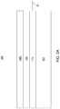
- FIG. 4A illustrates a cubic unit cell of BiFeO 3 with a direction of ferroelectric polarization P along a [111] direction and a canted magnetic moment direction Mc within the (111) plane.
- FIG. 4B illustrates the in plane (100) and out of plane (001) components of the magnetic moment direction Mc in the (111) plane.
- the relative spatial orientation e.g., 90 degree angle
- the out of plane (001) component of the canted magnetic moment direction Mc of each multiferroic portion is magnetically coupled to the magnetization direction of corresponding free layer via exchange bias or coupling at their interface.
- a change in the canted magnetic moment direction Mc of each multiferroic portion also changes the magnetization direction of the corresponding free layer (which may be a standalone free layer such as a first free layer 136 A, a second free layer 136 B, or a third free layer 136 C, or a portion 136 _ i of a continuous free layer 136 L) which contacts the respective multiferroic portion ( 148 A, 148 B, 148 C or 248 _ i ).
- the change in the magnetization direction of the free layer puts the free layer in either the parallel or antiparallel configuration with the magnetization direction of the correspond reference layer in the same magnetic tunnel junction.
- the parallel or antiparallel configuration of the free and reference layer magnetization directions places the magnetic tunnel junction either in the low or high resistance state, respectively.
- the free layers may comprise a set of discrete free layers (such as a set of a first free layer 136 A, a second free layer 136 B, and a third free layer 136 C) or as a set of multiple grains ( 136 _ i, 1 ⁇ i ⁇ N) of a free layer 136 L of which the magnetization direction can flip independently.
- the magnetization within each magnetoelectric multiferroic portion ⁇ ( 148 A, 148 B, 148 C) or ( 248 _ i, 1 ⁇ i ⁇ N) ⁇ can flip independently at different electric coercivities due to the different structural defect densities therein.
- a magnetoelectric multiferroic portion ⁇ ( 148 A, 148 B, 148 C) or ( 248 _ i, 1 ⁇ i ⁇ N) ⁇ having a higher structural defect density has a higher ferroelectric coercivity than a magnetoelectric multiferroic portion ⁇ ( 148 A, 148 B, 148 C) or ( 248 _ i, 1 ⁇ i ⁇ N) ⁇ having a lower structural defect density.
- a higher structural defect density flip i.e., switch
- Such multiple free layers with different magnetization directions result in multiple spin alignment states between the reference layer(s) ⁇ ( 132 A, 132 B, 132 C) or 132 L ⁇ and the respective free layers ⁇ ( 136 A, 136 B, 136 C) or 136 _ i ⁇ in the respective magnetic tunnel junctions ( 140 A, 140 B, 140 C or 140 _ i ).
- the magnetoresistance of a magnetic tunnel junction device 180 of the various embodiments of the present disclosure can have three or more values for the magnetoresistance between the top electrode 110 and the bottom electrode 170 .
- the total number of magnetoresistive states in a magnetic tunnel junction device 180 of the various embodiments of the present disclosure can be the same as the total number of magnetoelectric multiferroic portions ⁇ ( 148 A, 148 B, 148 C) or ( 248 _ i, 1 ⁇ i ⁇ N) ⁇ having different ferroelectric coercivities plus one.
- FIG. 5 illustrates the tunnel magnetoresistance as a function of the applied electrical field (i.e., programming voltage) across the magnetoelectric multiferroic portions ( 148 A, 148 B, 148 C) in the exemplary magnetic tunnel junction device of FIG. 2D .
- the graph in FIG. 5 is normalized along the horizontal axis by the magnitude of the maximum electrical field E max that can be applied between the top electrode 110 and the bottom electrode 170 . Further, the graph in FIG. 5 is normalized along the vertical axis by the minimum magnetoresistance of the exemplary magnetic tunnel junction device of FIG. 2D . If three magnetoelectric multiferroic portions ( 148 A, 148 B, 148 C) are present in the exemplary magnetic tunnel junction device of FIG.
- four magnetoresistive states can be formed as a function of the applied programming voltage between the top electrode 110 and the bottom electrode 170 .
- the direction of magnetization of the reference layers ( 132 A, 132 B, 132 C) is presumed to be downward, parallel alignment of spins between each reference layer ( 132 A, 132 B, 132 C) and an underlying free layer ( 136 A, 136 B, 136 C) is presumed to provide a lower magnetoresistance than antiparallel alignment, and the directions of the arrows represent the directions of the magnetizations of the three free layers ( 136 A, 136 B, 136 C).
- the application of positive and negative programming voltages may deterministically switch the magnetization direction of the free layers back and forth without application of an external magnetic field.
- Different absolute values (i.e., magnitudes) of the critical positive and negative programming voltages are able to switch the magnetization direction of one, two or all three free layers in the device 180 .
- a lowest absolute value of the critical positive programming voltage is able to switch the magnetization direction of only one free layer 136 C which is magnetically coupled to the respective multiferroic region 148 C with the lowest density of structural defects.
- the device is switched from magnetoresistive state 1 to state 2 in FIG. 5 .
- a middle absolute value of the critical positive programming voltage is able to switch the magnetization of two free layers ( 136 B, 136 C) which are magnetically coupled to the respective multiferroic regions ( 148 B, 148 C) with the middle and lowest density of structural defects.
- the device is switched from magnetoresistive state 2 to state 3 in FIG. 5 .
- the magnetization direction of the free layer 136 A which is magnetically coupled to the respective multiferroic region 148 A with the highest density of structural defects is not switched.
- a highest absolute value of the critical positive programming voltage is able to switch the magnetization direction of all three free layers ( 136 A, 136 B, 136 C) which are magnetically coupled to the respective multiferroic regions ( 148 A, 148 B, 148 C).
- the device is switched from magnetoresistive state 3 to state 4 in FIG. 5 .
- four magnetoresistive states may be obtained in a device 180 containing three free layers and three multiferroic regions. The same four states may be achieved in reverse (i.e., from state 4 to state 1 ) using different absolute values (i.e., magnitudes) of the critical negative programming voltages.
- At least two magnetoelectric multiferroic portions ⁇ ( 148 A, 148 B, 148 C) or ( 248 _ i, 1 ⁇ i ⁇ N) ⁇ can be provided within each magnetic tunnel junction device 180 .
- the magnetoresistance between the bottom electrode 170 and the top electrode 110 can have at least three different values that depend on magnetization directions of the plurality of magnetoelectric multiferroic portions in each magnetic tunnel junction device 180 of the present disclosure.
- the magnetic tunnel junction devices 180 of the embodiments of the present disclosure can be connected in a synaptic connection configuration.
- the magnetic tunnel junction devices 180 can be connected in a synaptic connection configuration in which output nodes of one group of magnetic tunnel junction devices 180 are connected to a respective set of multiple input nodes of another group of magnetic tunnel junction devices 180 .
- the average number of connections per output node of each magnetic tunnel junction device 180 may be at least three, and may be four or more.
- the connections within the synaptic connection configurations may be confined within physical proximity of each magnetic tunnel junction device.
- the electrical connection may be limited up to second nearest neighbor magnetic tunnel junction devices, third nearest neighbor magnetic tunnel junction devices, fourth nearest neighbor ferroelectric devices, or any other predetermined level of physical proximity.
- Such synaptic connection configuration can be advantageously employed to provide a computing device in which multiple possibilities are simultaneously calculated, and probabilistic answers to a given question are provided.
- the conductance of each path can increase within an increase of respective control voltage in such a synaptic connection configuration.
- the path that provides the most electrical current under a set of predetermined control voltages (such as a set of bias voltages to a selected subset of the magnetic tunnel junction devices 180 ) can be determined within a timeframe of nanoseconds.
- a magnetic tunnel junction device 180 containing a tunnel barrier layer 134 e.g., MgO layer
- MRAM spintronic
- a spin valve or pseudo spin valve giant magnetoresistive (GMR) device may be formed instead.
- the tunneling barrier layer is replaced with an electrically conductive, non-magnetic spacer layer.
- a spin valve device typically includes the SAF structure which pins the reference layer. The SAF structure may be omitted in the pseudo spin valve device, and different ferromagnetic materials having different coercivities may be used for the free layer and the reference layer.
- the spin valve and pseudo spin valve devices may be formed over or under the multiferroic portions which are coupled to the respective free layers.
- a magnetic device 180 includes a first electrode 170 , a second electrode, 110 a plurality of magnetic junctions 140 each containing a ferromagnetic reference layer 132 and a ferromagnetic free layer 136 located between the first electrode and the second electrode, and a plurality of magnetoelectric multiferroic portions ⁇ ( 148 A, 148 B, 148 C) or ( 248 _ i ) ⁇ having different structural defect densities located between the first electrode and the second electrode.
- Each of the plurality of magnetoelectric multiferroic portions is magnetically coupled to the ferromagnetic free layer 136 of a respective one of the plurality of magnetic junctions 140 .
- the plurality of magnetic junctions 140 comprise a plurality of magnetic tunnel junctions ⁇ ( 140 A, 140 B, 140 C), or ( 140 _ i, 1 ⁇ i ⁇ N) ⁇ , each comprising a respective reference layer ( 132 A, 132 B, 132 C, or a portion of 132 L), a respective tunnel barrier layer ( 134 A, 134 B, 134 C, or a portion of 134 L), and a respective ferromagnetic free layer ( 136 A, 136 B, 136 C, or a portion of 136 L).
- the plurality of magnetoelectric multiferroic portions ⁇ ( 148 A, 148 B, 148 C) or ( 248 _ i ⁇ comprise, and/or consist essentially of, a material selected from BiFeO 3 , h-YMnO 3 , BaNiF 4 , PbVO 3 , BiMnO 3 , LuFe 2 O 4 , HoMn 2 O 5 , h-HoMnO 3 , h-ScMnO 3 , h-ErMnO 3 , h-TmMnO 3 , h-YbMnO 3 , h-LuMnO 3 , K 2 SeO 4 , Cs 2 CdI 4 , TbMnO 3 , Ni 3 V 2 O 8 , MnWO 4 , CuO, ZnCr 2 Se 4 , LiCu 2 O 2 , or Ni 3 B 7 O 13 I.
- each of the plurality of magnetoelectric multiferroic portion ⁇ ( 148 A, 148 B, 148 C) or ( 248 _ i ⁇ has a respective canted magnetic moment direction Mc and a respective ferroelectric polarization direction P.
- a relative spatial orientation between the respective canted magnetic moment direction and a respective ferroelectric polarization direction within each magnetoelectric multiferroic portion is the same.
- Each magnetoelectric multiferroic portion ⁇ ( 148 A, 148 B, 148 C) or ( 248 _ i ⁇ contacts a respective ferromagnetic free layer ( 136 A, 136 B, 136 C, or a portion of 136 L), and has a respective out of plane (e.g., (001)) component of the canted magnetic moment that is magnetically coupled to the respective free layer via exchange coupling or bias.
- a respective out of plane e.g., (001)
- magnetoresistance between the first electrode 170 and the second electrode 110 has at least three different values that depend on the respective canted magnetic moment direction Mc of the plurality of magnetoelectric multiferroic portions and the magnetization direction of the respective magnetically coupled free layer relative to the magnetization direction of the reference layer in the same magnetic junction.
- the first electrode 170 comprises a bottom electrode
- the second electrode 110 comprises a top electrode located over the bottom electrode
- the plurality of magnetic junctions 140 are located above or below the plurality of magnetoelectric multiferroic portions.
- the different structural defect densities may comprise a different density of broken bonds in the different magnetoelectric multiferroic portions, a different density of displaced atoms in a crystal lattice in the different magnetoelectric multiferroic portions, and/or a different density of gallium or helium atoms in the different magnetoelectric multiferroic portions.
- the plurality of magnetoelectric multiferroic portions comprise a first magnetoelectric multiferroic portion 148 A having a first structural defect density and a first ferroelectric coercivity, and a second magnetoelectric multiferroic portion 148 B having a second structural defect density higher than the first structural defect density, and a second ferroelectric coercivity higher than the first ferroelectric coercivity.
- the plurality of magnetic junctions 140 comprise discrete magnetic tunnel junctions ( 140 A, 140 B, 140 C) that do not directly contact one another and the plurality of magnetoelectric multiferroic portions ( 148 A, 148 B, 148 C) are separated by distinct boundaries 146 .
- the plurality of magnetoelectric multiferroic portions 248 _ i lack distinct boundaries within a single continuous magnetoelectric multiferroic layer 248 and have a graded structural defect density that monotonically laterally changes from one side to another, and the plurality of magnetic junctions 140 _ i comprise a continuous polycrystalline ferromagnetic free layer 136 L having a plurality of grains separated by domain wall grain boundaries.
- the various embodiments of the present disclosure provide a magnetic junction device 180 including three or more magnetoresistive states.
- the magnetic junction device 180 can be provided as a single standalone device.
- plural magnetic junction devices 180 may be arranged in an array configuration or a synaptic connection configuration to provide a random access memory (e.g., a magnetoresistive memory) device or a synaptic configuration computing device.
- a random access memory e.g., a magnetoresistive memory
- a method of forming a plurality of magnetoelectric multiferroic portions in a continuous magnetoelectric multiferroic layer comprises structurally damaging different portions of the continuous magnetoelectric multiferroic layer with different structural defect densities.
- structurally damaging different portions of the continuous magnetoelectric multiferroic layer comprises performing a different focused ion beam irradiation process in each of the plurality of magnetoelectric multiferroic portions to provide the different structural defect densities in each of the plurality of the magnetoelectric multiferroic portions.
- the different focused ion beam irradiation processes may result in at least one of a different density of broken bonds in different magnetoelectric multiferroic portions, a different density of displaced atoms in a crystal lattice in the different magnetoelectric multiferroic portions, or different density of gallium or helium atoms in the different magnetoelectric multiferroic portions.
- the method includes forming discrete magnetic tunnel junctions that do not direct contact one formed above or below magnetoelectric multiferroic portions separated by distinct boundaries.
- the focused ion beam irradiation generates a graded structural defect density that monotonically laterally changes from one side to another within the continuous magnetoelectric multiferroic layer.
- a continuous magnetic tunnel junction stack is formed over the continuous magnetoelectric multiferroic layer, where different regions of the continuous magnetic tunnel junction stack comprise plurality of magnetic junctions.
Landscapes
- Engineering & Computer Science (AREA)
- Chemical & Material Sciences (AREA)
- Physics & Mathematics (AREA)
- Theoretical Computer Science (AREA)
- Power Engineering (AREA)
- Crystallography & Structural Chemistry (AREA)
- Life Sciences & Earth Sciences (AREA)
- Molecular Biology (AREA)
- General Health & Medical Sciences (AREA)
- Biomedical Technology (AREA)
- Health & Medical Sciences (AREA)
- Manufacturing & Machinery (AREA)
- Computer Hardware Design (AREA)
- Artificial Intelligence (AREA)
- Computational Linguistics (AREA)
- Data Mining & Analysis (AREA)
- Evolutionary Computation (AREA)
- Computing Systems (AREA)
- General Engineering & Computer Science (AREA)
- General Physics & Mathematics (AREA)
- Mathematical Physics (AREA)
- Software Systems (AREA)
- Biophysics (AREA)
- Neurology (AREA)
- Mram Or Spin Memory Techniques (AREA)
- Hall/Mr Elements (AREA)
Abstract
Description
Claims (20)
Priority Applications (3)
| Application Number | Priority Date | Filing Date | Title |
|---|---|---|---|
| US16/781,225 US11222920B2 (en) | 2020-02-04 | 2020-02-04 | Magnetic device including multiferroic regions and methods of forming the same |
| CN202080079838.8A CN114730589A (en) | 2020-02-04 | 2020-06-02 | Magnetic device including multiferroic region and method of forming the same |
| PCT/US2020/035649 WO2021158250A1 (en) | 2020-02-04 | 2020-06-02 | Magnetic device including multiferroic regions and methods of forming the same |
Applications Claiming Priority (1)
| Application Number | Priority Date | Filing Date | Title |
|---|---|---|---|
| US16/781,225 US11222920B2 (en) | 2020-02-04 | 2020-02-04 | Magnetic device including multiferroic regions and methods of forming the same |
Publications (2)
| Publication Number | Publication Date |
|---|---|
| US20210242279A1 US20210242279A1 (en) | 2021-08-05 |
| US11222920B2 true US11222920B2 (en) | 2022-01-11 |
Family
ID=77062380
Family Applications (1)
| Application Number | Title | Priority Date | Filing Date |
|---|---|---|---|
| US16/781,225 Active 2040-03-26 US11222920B2 (en) | 2020-02-04 | 2020-02-04 | Magnetic device including multiferroic regions and methods of forming the same |
Country Status (3)
| Country | Link |
|---|---|
| US (1) | US11222920B2 (en) |
| CN (1) | CN114730589A (en) |
| WO (1) | WO2021158250A1 (en) |
Citations (40)
| Publication number | Priority date | Publication date | Assignee | Title |
|---|---|---|---|---|
| US5198994A (en) | 1988-08-31 | 1993-03-30 | Kabushiki Kaisha Toshiba | Ferroelectric memory device |
| US20010048622A1 (en) | 2000-05-31 | 2001-12-06 | O-Sung Kwon | Method for manufacturing a ferroelectric random access memory device |
| EP0936622B1 (en) | 1998-02-10 | 2002-10-02 | International Business Machines Corporation | Magnetic memory devices having multiple magnetic tunnel junctions therein |
| US20030053350A1 (en) | 2001-08-13 | 2003-03-20 | Krieger Juri H. | Memory device |
| US20030155602A1 (en) | 2001-08-13 | 2003-08-21 | Coatue Corporation | Memory device |
| US20030178667A1 (en) | 2001-08-13 | 2003-09-25 | Krieger Juri H. | Memory device |
| US20050151177A1 (en) | 2003-11-05 | 2005-07-14 | Hiromu Miyazawa | Ferroelectric film, ferroelectric capacitor, and ferroelectric memory |
| JP2006210525A (en) | 2005-01-26 | 2006-08-10 | Sony Corp | Memory device and circuit element |
| US20070020803A1 (en) | 2005-07-19 | 2007-01-25 | Fujitsu Limited | Semiconductor device and manufacturing method of the same |
| US20090026513A1 (en) | 2005-05-10 | 2009-01-29 | Thin Film Electronics Asa | Method for forming ferroelectric thin films, the use of the method and a memory with a ferroelectric oligomer memory material |
| US20090073747A1 (en) | 2007-09-17 | 2009-03-19 | Seagate Technology Llc | Magnetoresistive sensor memory with multiferroic material |
| US7750390B2 (en) * | 2006-01-17 | 2010-07-06 | Kabushiki Kaisha Toshiba | Spin fet and spin memory |
| US20120069646A1 (en) * | 2010-09-17 | 2012-03-22 | Micron Technology, Inc. | Spin torque transfer memory cell structures and methods |
| US20120069647A1 (en) * | 2010-09-17 | 2012-03-22 | Micron Technology, Inc. | Spin torque transfer memory cell structures and methods |
| US20120069648A1 (en) * | 2010-09-17 | 2012-03-22 | Micron Technology, Inc. | Spin torque transfer memory cell structures and methods |
| US20120104325A1 (en) | 2009-04-23 | 2012-05-03 | The University Of Chicago | Materials and Methodss for the Preparation of Nanocomposites |
| WO2013090937A1 (en) | 2011-12-16 | 2013-06-20 | Northeastern University | E-field writable non-volatile magnetic random access memory based on multiferroics |
| US20140098458A1 (en) | 2012-10-09 | 2014-04-10 | Saudi Basic Industries Corporation | Graphene-based composite materials, method of manufacture and applications thereof |
| US20150372225A1 (en) | 2014-06-20 | 2015-12-24 | International Business Machines Corporation | Method of forming an on-pitch self-aligned hard mask for contact to a tunnel junction using ion beam etching |
| US20160141333A1 (en) | 2014-11-18 | 2016-05-19 | Virginia Commonwealth University | Magneto-elastic non-volatile multiferroic logic and memory with ultralow energy dissipation |
| US20160172365A1 (en) | 2014-11-02 | 2016-06-16 | Thomas J. McKinnon | Ferroelectric memory device and fabrication process thereof, and methods for operation thereof |
| EP3128534A2 (en) | 2015-08-07 | 2017-02-08 | IMEC vzw | Ferroelectric memory device and fabrication method thereof |
| US20170114241A1 (en) | 2014-06-09 | 2017-04-27 | Sabic Global Technologies B.V. | Processing of thin film organic ferroelectric materials using pulsed electromagnetic radiation |
| US9646666B2 (en) * | 2015-02-02 | 2017-05-09 | Globalfoundries Singapore Pte. Ltd. | Voltage controlled spin switches for low power applications |
| US9721963B1 (en) | 2016-04-08 | 2017-08-01 | Sandisk Technologies Llc | Three-dimensional memory device having a transition metal dichalcogenide channel |
| US20170316713A1 (en) | 2004-04-30 | 2017-11-02 | Sydney Hyman | Image making medium compositions and images |
| US9817088B2 (en) * | 2015-03-19 | 2017-11-14 | Globalfoundries Singapore Pte. Ltd. | Voltage-tunable magnetic devices for communication applications |
| US9941299B1 (en) | 2017-05-24 | 2018-04-10 | Sandisk Technologies Llc | Three-dimensional ferroelectric memory device and method of making thereof |
| US20180158934A1 (en) | 2016-11-21 | 2018-06-07 | The Government Of The United States Of America, As Represented By The Secretary Of The Navy | Lateral heterojunctions in two-dimensional materials integrated with multiferroic layers |
| US20180158955A1 (en) | 2016-11-21 | 2018-06-07 | The Government Of The United States Of America, As Represented By The Secretary Of The Navy | Controlling structural phase transitions and properties of two-dimensional materials by integrating with multiferroic layers |
| US20180158588A1 (en) * | 2015-06-24 | 2018-06-07 | Intel Corporation | Metallic spin super lattice for logic and memory devices |
| US20180287052A1 (en) * | 2016-12-02 | 2018-10-04 | Regents Of The University Of Minnesota | MAGNETIC STRUCTURES INCLUDING FePd |
| US20190027201A1 (en) | 2017-07-24 | 2019-01-24 | Sandisk Technologies Llc | Magnetoelectric random access memory array and methods of operating the same |
| US10229723B1 (en) | 2017-09-12 | 2019-03-12 | Sandisk Technologies Llc | Spin orbit torque magnetoresistive random access memory containing composite spin hall effect layer including beta phase tungsten |
| US10381551B1 (en) | 2018-06-29 | 2019-08-13 | Sandisk Technologies Llc | Spin orbit torque magnetoresistive random access memory containing shielding element and method of making thereof |
| US20190252015A1 (en) * | 2018-02-13 | 2019-08-15 | Micron Technology, Inc. | Enabling fast pulse operation |
| US20190386202A1 (en) * | 2018-06-19 | 2019-12-19 | Intel Corporation | Spin orbit memory with multiferroic material |
| US20190386208A1 (en) * | 2018-06-14 | 2019-12-19 | Intel Corporation | Transition metal dichalcogenide based magneto-electric memory device |
| US20200006633A1 (en) | 2018-06-29 | 2020-01-02 | Sandisk Technologies Llc | Spin orbit torque magnetoresistive random access memory containing shielding element and method of making thereof |
| US20200211608A1 (en) * | 2016-12-13 | 2020-07-02 | Intel Corporation | Perpendicular magnetoelectric spin orbit logic |
-
2020
- 2020-02-04 US US16/781,225 patent/US11222920B2/en active Active
- 2020-06-02 CN CN202080079838.8A patent/CN114730589A/en active Pending
- 2020-06-02 WO PCT/US2020/035649 patent/WO2021158250A1/en active Application Filing
Patent Citations (49)
| Publication number | Priority date | Publication date | Assignee | Title |
|---|---|---|---|---|
| US5198994A (en) | 1988-08-31 | 1993-03-30 | Kabushiki Kaisha Toshiba | Ferroelectric memory device |
| EP0936622B1 (en) | 1998-02-10 | 2002-10-02 | International Business Machines Corporation | Magnetic memory devices having multiple magnetic tunnel junctions therein |
| US20010048622A1 (en) | 2000-05-31 | 2001-12-06 | O-Sung Kwon | Method for manufacturing a ferroelectric random access memory device |
| US20030053350A1 (en) | 2001-08-13 | 2003-03-20 | Krieger Juri H. | Memory device |
| US20030155602A1 (en) | 2001-08-13 | 2003-08-21 | Coatue Corporation | Memory device |
| US20030178667A1 (en) | 2001-08-13 | 2003-09-25 | Krieger Juri H. | Memory device |
| US20030179633A1 (en) | 2001-08-13 | 2003-09-25 | Krieger Juri H. | Memory device |
| US20040026729A9 (en) | 2001-08-13 | 2004-02-12 | Coatue Corporation | Memory device |
| US20040159835A1 (en) | 2001-08-13 | 2004-08-19 | Krieger Juri Heinrich | Memory device |
| US20050151177A1 (en) | 2003-11-05 | 2005-07-14 | Hiromu Miyazawa | Ferroelectric film, ferroelectric capacitor, and ferroelectric memory |
| US20170316713A1 (en) | 2004-04-30 | 2017-11-02 | Sydney Hyman | Image making medium compositions and images |
| JP2006210525A (en) | 2005-01-26 | 2006-08-10 | Sony Corp | Memory device and circuit element |
| US20090026513A1 (en) | 2005-05-10 | 2009-01-29 | Thin Film Electronics Asa | Method for forming ferroelectric thin films, the use of the method and a memory with a ferroelectric oligomer memory material |
| US20100144064A1 (en) | 2005-07-19 | 2010-06-10 | Fujitsu Microelectronics Limited | Semiconductor device having a ferroelectric capacitor |
| US20070020803A1 (en) | 2005-07-19 | 2007-01-25 | Fujitsu Limited | Semiconductor device and manufacturing method of the same |
| US7750390B2 (en) * | 2006-01-17 | 2010-07-06 | Kabushiki Kaisha Toshiba | Spin fet and spin memory |
| US20090073747A1 (en) | 2007-09-17 | 2009-03-19 | Seagate Technology Llc | Magnetoresistive sensor memory with multiferroic material |
| US20120104325A1 (en) | 2009-04-23 | 2012-05-03 | The University Of Chicago | Materials and Methodss for the Preparation of Nanocomposites |
| US20160308107A1 (en) | 2009-04-23 | 2016-10-20 | The University Of Chicago | Materials and methods for the preperation of nanocomposites |
| US20120069646A1 (en) * | 2010-09-17 | 2012-03-22 | Micron Technology, Inc. | Spin torque transfer memory cell structures and methods |
| US20120069648A1 (en) * | 2010-09-17 | 2012-03-22 | Micron Technology, Inc. | Spin torque transfer memory cell structures and methods |
| US20120069647A1 (en) * | 2010-09-17 | 2012-03-22 | Micron Technology, Inc. | Spin torque transfer memory cell structures and methods |
| WO2013090937A1 (en) | 2011-12-16 | 2013-06-20 | Northeastern University | E-field writable non-volatile magnetic random access memory based on multiferroics |
| US20140098458A1 (en) | 2012-10-09 | 2014-04-10 | Saudi Basic Industries Corporation | Graphene-based composite materials, method of manufacture and applications thereof |
| US20170114241A1 (en) | 2014-06-09 | 2017-04-27 | Sabic Global Technologies B.V. | Processing of thin film organic ferroelectric materials using pulsed electromagnetic radiation |
| US20150372225A1 (en) | 2014-06-20 | 2015-12-24 | International Business Machines Corporation | Method of forming an on-pitch self-aligned hard mask for contact to a tunnel junction using ion beam etching |
| US20160276579A1 (en) | 2014-06-20 | 2016-09-22 | International Business Machines Corporation | Method of forming an on-pitch self-aligned hard mask for contact to a tunnel junction using ion beam etching |
| US20160172365A1 (en) | 2014-11-02 | 2016-06-16 | Thomas J. McKinnon | Ferroelectric memory device and fabrication process thereof, and methods for operation thereof |
| US20160141333A1 (en) | 2014-11-18 | 2016-05-19 | Virginia Commonwealth University | Magneto-elastic non-volatile multiferroic logic and memory with ultralow energy dissipation |
| US9646666B2 (en) * | 2015-02-02 | 2017-05-09 | Globalfoundries Singapore Pte. Ltd. | Voltage controlled spin switches for low power applications |
| US9817088B2 (en) * | 2015-03-19 | 2017-11-14 | Globalfoundries Singapore Pte. Ltd. | Voltage-tunable magnetic devices for communication applications |
| US20180158588A1 (en) * | 2015-06-24 | 2018-06-07 | Intel Corporation | Metallic spin super lattice for logic and memory devices |
| EP3128534A2 (en) | 2015-08-07 | 2017-02-08 | IMEC vzw | Ferroelectric memory device and fabrication method thereof |
| US9721963B1 (en) | 2016-04-08 | 2017-08-01 | Sandisk Technologies Llc | Three-dimensional memory device having a transition metal dichalcogenide channel |
| US10403753B2 (en) | 2016-11-21 | 2019-09-03 | The Government Of The United States Of America, As Represented By The Secretary Of The Navy | Controlling structural phase transitions and properties of two-dimensional materials by integrating with multiferroic layers |
| US20180158934A1 (en) | 2016-11-21 | 2018-06-07 | The Government Of The United States Of America, As Represented By The Secretary Of The Navy | Lateral heterojunctions in two-dimensional materials integrated with multiferroic layers |
| US20180158955A1 (en) | 2016-11-21 | 2018-06-07 | The Government Of The United States Of America, As Represented By The Secretary Of The Navy | Controlling structural phase transitions and properties of two-dimensional materials by integrating with multiferroic layers |
| US20180287052A1 (en) * | 2016-12-02 | 2018-10-04 | Regents Of The University Of Minnesota | MAGNETIC STRUCTURES INCLUDING FePd |
| US20200211608A1 (en) * | 2016-12-13 | 2020-07-02 | Intel Corporation | Perpendicular magnetoelectric spin orbit logic |
| US9941299B1 (en) | 2017-05-24 | 2018-04-10 | Sandisk Technologies Llc | Three-dimensional ferroelectric memory device and method of making thereof |
| US20190027201A1 (en) | 2017-07-24 | 2019-01-24 | Sandisk Technologies Llc | Magnetoelectric random access memory array and methods of operating the same |
| US10354710B2 (en) | 2017-07-24 | 2019-07-16 | Sandisk Technologies Llc | Magnetoelectric random access memory array and methods of operating the same |
| US20190080738A1 (en) | 2017-09-12 | 2019-03-14 | Sandisk Technologies Llc | Spin orbit torque magnetoresistive random access memory containing composite spin hall effect layer including beta phase tungsten |
| US10229723B1 (en) | 2017-09-12 | 2019-03-12 | Sandisk Technologies Llc | Spin orbit torque magnetoresistive random access memory containing composite spin hall effect layer including beta phase tungsten |
| US20190252015A1 (en) * | 2018-02-13 | 2019-08-15 | Micron Technology, Inc. | Enabling fast pulse operation |
| US20190386208A1 (en) * | 2018-06-14 | 2019-12-19 | Intel Corporation | Transition metal dichalcogenide based magneto-electric memory device |
| US20190386202A1 (en) * | 2018-06-19 | 2019-12-19 | Intel Corporation | Spin orbit memory with multiferroic material |
| US10381551B1 (en) | 2018-06-29 | 2019-08-13 | Sandisk Technologies Llc | Spin orbit torque magnetoresistive random access memory containing shielding element and method of making thereof |
| US20200006633A1 (en) | 2018-06-29 | 2020-01-02 | Sandisk Technologies Llc | Spin orbit torque magnetoresistive random access memory containing shielding element and method of making thereof |
Non-Patent Citations (40)
| Title |
|---|
| Ahn et al., "Energy-Efficient Phase-Change Memory with Graphene as a Thermal Barrier," Nano Letters, 15, 6809 (2015). |
| Cadore et al., "Thermo Activated Hysteresis on High Quality Graphene/h-BN Devices," Nano Lett. 14, 5437 (2014). |
| Chiu, Y.C. et al., "Multilevel nonvolatile transistor memories using a star-shaped poly((4-diphenylamino)benzyl methacrylate) gate electret," NPG Asia Materials (2013), vol. 5, e35; doi:10.1038/am.2012.64, available at https://www.nature.com/articles/am201264. |
| Heron, J. T. et al., "Electric field control of magnetism using BiFeO3-based heterostructures," Applied Physics Reviews, vol. 1, 021303 (2014); doi: 10.1063/1.4870957, View online: http://dx.doi.org/10.1063/1.4870957. |
| Huang et al., "Graphene/Si CMOS Hybrid Hall Integrated Circuits," Science Reports, 4, 5548 (2014). |
| Ismach et al., "Direct Chemical Vapor Deposition of Graphene on Dielectric Surfaces," Nano Letters, 10, 1542 (2010). |
| Jerry, M. et al., "Ferroelectric FET Analog Synapse for Acceleration of Deep Neural Network Training," Tech. Dig.—Int. Electron Devices Meeting (IEDM), IEEE, San Francisco, CA 2017, p. 6.2.1-6.2.4, IEDM17-139 (Published—Jan. 23, 2018). |
| Lequex, S. et al., "A magnetic synapse: multilevel spin-torque memristor with perpendicular anisotropy" Scientific Reports, vol. 6, No. 31510 (2016), https://doi.org/10.1038/srep31510. |
| Manipatruni, S. et al., "Beyond CMOS computing with spin and polarization," Nature Physics, vol. 14, pp. 338-343, (2018), https://doi.org/10.1038/s41567-018-0101-4. |
| Miro et al., "An Atlas of Two-Dimensional Materials," Chem. Soc. Rev., 2014,43, 6537-6554. |
| Morelli, A., et al., "Epitaxial Ferroelectric Nanostructures Fabricated by FIB Milling," (Abstract) In: Wang Z. (eds) FIB Nanostructures. Lecture Notes in Nanoscale Science and Technology, vol. 20. Springer, Cham, (2013), https://doi.org/10.1007/978-3-319-02874-3_2. |
| Notification of Transmittal of the International Search Report and Written Opinion of the International Search Authority for International Patent Application No. PCT/US2019/046717, dated Nov. 17, 2019, 11 pages. |
| Notification of Transmittal of the International Search Report and Written Opinion of the International Search Authority for International Patent Application No. PCT/US2020/035649, dated Sep. 24, 2020, 13 pages. |
| Saremi, S. et al., "Electronic Transport and Ferroelectric Switching in Ion-Bombarded, Defect-Engineered BiFeO3 Thin Films," Adv. Mater. Interfaces 2018, vol. 5, 1700991, (2018). |
| Saremi, S. et al., "Local Control of Defects and Switching Properties in Ferroelectric Thin Films," Phys. Rev. Mater., vol. 2, 084414 (2018). |
| Sengupta, A. et al., "Encoding neural and synaptic functionalities in electron spin: A pathway to efficient neuromorphic computing," Applied Physics Reviews 4, 041105 (2017); https://doi.org/10.1063/1.5012763. |
| Song et al., "Robust bi-stable Memory Operation in Single-layer Graphene Ferroelectric Memory," Appl. Phys. Lett. 99, 042109 (2011). |
| Spaldin, N. A. et al., "Advances in magnetoelectric multiferroics," Nature Materials, vol. 18, pp. 203-212, (2019), https://doi.org/10.1038/s41563-018-0275-2. |
| Srinivasan, G. et al., "Magnetic Tunnel Junction Based Long-Term Short-Term Stochastic Synapse for a Spiking Neural Network with On-Chip STDP Learning," Scientific reports 6 (2016): 29545, DOI: 10.1038/srep29545. |
| U.S. Appl. No. 16/212,132, filed Dec. 6, 2018, SanDisk Technologies LLC. |
| U.S. Appl. No. 16/212,257, filed Dec. 6, 2018, SanDisk Technologies LLC. |
| U.S. Appl. No. 16/212,342, filed Dec. 6, 2018, SanDisk Technologies LLC. |
| U.S. Appl. No. 16/212,420, filed Dec. 6, 2018, SanDisk Technologies LLC. |
| U.S. Appl. No. 16/227,889, filed Dec. 20, 2018, SanDisk Technologies LLC. |
| U.S. Appl. No. 16/250,403, filed Jan. 17, 2019, SanDisk Technologies LLC. |
| U.S. Appl. No. 16/401,172, filed May 2, 2019, SanDisk Technologies LLC. |
| U.S. Appl. No. 16/419,243, filed May 22, 2019, SanDisk Technologies LLC. |
| U.S. Appl. No. 16/422,187, filed May 24, 2019, SanDisk Technologies LLC. |
| U.S. Appl. No. 16/442,858, filed Jun. 17, 2019, SanDisk Technologies LLC. |
| U.S. Appl. No. 16/558,552, filed Sep. 3, 2019, SanDisk Technologies LLC. |
| U.S. Appl. No. 16/666,967, filed Oct. 29, 2019, SanDisk Technologies LLC. |
| U.S. Appl. No. 16/686,860, filed Nov. 18, 2019, SanDisk Technologies LLC. |
| U.S. Appl. No. 16/686,917, filed Nov. 18, 2019, SanDisk Technologies LLC. |
| U.S. Appl. No. 16/692,903, filed Nov. 22, 2019, SanDisk Technologies LLC. |
| U.S. Appl. No. 16/692,965, filed Nov. 22, 2019, SanDisk Technologies LLC. |
| U.S. Appl. No. 16/693,006, filed Nov. 22, 2019, SanDisk Technologies LLC. |
| U.S. Appl. No. 16/778,245, filed Jan. 31, 2020, SanDisk Technologies LLC. |
| Xu, T. et al., "Defect-strain engineering for multiferroic and magnetoelectric properties in epitaxial (110) ferroelectric lead titanate," (Abstract) Phys. Rev. B 92, 104106—Published Sep. 14, 2015. |
| Zheng et al., "Gate-controlled Non-Volatile Graphene-ferroelectric Memory," Appl. Phys. Lett. 94, 163505 (2009). |
| Zheng et al., "Graphene Field Effect Transistors with Ferroelectric Gating," Phys. Rev. Lett. 105, 166602 (2010). |
Also Published As
| Publication number | Publication date |
|---|---|
| CN114730589A (en) | 2022-07-08 |
| WO2021158250A1 (en) | 2021-08-12 |
| US20210242279A1 (en) | 2021-08-05 |
Similar Documents
| Publication | Publication Date | Title |
|---|---|---|
| KR102617167B1 (en) | Memory cell with magnetic tunnel junction and thermal stability enhancement layer | |
| GB2539102B (en) | Voltage-controlled magnetic anisotropy switching device using an external ferromagnetic biasing film | |
| US8138561B2 (en) | Structure and method to fabricate high performance MTJ devices for spin-transfer torque (STT)-RAM | |
| KR102375641B1 (en) | Magnetic random access memory assisted devices and methods of making | |
| US7078244B2 (en) | Multi-bit MRAM device with switching nucleation sites | |
| KR20080078079A (en) | Current switched spin transfer magnetic devices with reduced spin transfer switching current density | |
| US11005034B1 (en) | Magnetoresistive memory device including a high dielectric constant capping layer and methods of making the same | |
| US11404193B2 (en) | Magnetoresistive memory device including a magnesium containing dust layer | |
| US20210159392A1 (en) | Magnetoresistive memory device including a high dielectric constant capping layer and methods of making the same | |
| US10991407B1 (en) | Magnetoresistive memory device including a high dielectric constant capping layer and methods of making the same | |
| US11839162B2 (en) | Magnetoresistive memory device including a plurality of reference layers | |
| US11404632B2 (en) | Magnetoresistive memory device including a magnesium containing dust layer | |
| WO2021101585A1 (en) | Magnetoresistive memory device including a high dielectric constant capping layer and methods of making the same | |
| US11631716B2 (en) | Cross-point spin-transfer torque magnetoresistive memory array and method of making the same | |
| US11361805B2 (en) | Magnetoresistive memory device including a reference layer side dielectric spacer layer | |
| KR102589614B1 (en) | Magnetic memory device fabrication method using Ru and diamond-like carbon hard masks | |
| WO2021216137A1 (en) | Tunneling metamagnetic resistance memory device and methods of operating the same | |
| US11723217B2 (en) | Magnetic tunnel junction element with RU hard mask for use in magnetic random-access memory | |
| US11222920B2 (en) | Magnetic device including multiferroic regions and methods of forming the same | |
| US20220246842A1 (en) | Method for manufacturing a magnetic random-access memory device using post pillar formation annealing | |
| US11264562B1 (en) | Multiferroic-assisted voltage controlled magnetic anisotropy memory device and methods of manufacturing the same | |
| US11276446B1 (en) | Multiferroic-assisted voltage controlled magnetic anisotropy memory device and methods of manufacturing the same | |
| KR20040084095A (en) | A method for manufacturing of a Magnetic random access memory |
Legal Events
| Date | Code | Title | Description |
|---|---|---|---|
| FEPP | Fee payment procedure |
Free format text: ENTITY STATUS SET TO UNDISCOUNTED (ORIGINAL EVENT CODE: BIG.); ENTITY STATUS OF PATENT OWNER: LARGE ENTITY |
|
| AS | Assignment |
Owner name: WESTERN DIGITAL TECHNOLOGIES, INC.,, CALIFORNIA Free format text: ASSIGNMENT OF ASSIGNORS INTEREST;ASSIGNORS:PRASAD, BHAGWATI;KALITSOV, ALAN;REEL/FRAME:051986/0884 Effective date: 20200203 |
|
| AS | Assignment |
Owner name: JPMORGAN CHASE BANK, N.A., AS AGENT, ILLINOIS Free format text: SECURITY INTEREST;ASSIGNOR:WESTERN DIGITAL TECHNOLOGIES, INC.;REEL/FRAME:053482/0453 Effective date: 20200511 |
|
| STPP | Information on status: patent application and granting procedure in general |
Free format text: NON FINAL ACTION MAILED |
|
| STPP | Information on status: patent application and granting procedure in general |
Free format text: NOTICE OF ALLOWANCE MAILED -- APPLICATION RECEIVED IN OFFICE OF PUBLICATIONS |
|
| STPP | Information on status: patent application and granting procedure in general |
Free format text: PUBLICATIONS -- ISSUE FEE PAYMENT VERIFIED |
|
| STCF | Information on status: patent grant |
Free format text: PATENTED CASE |
|
| AS | Assignment |
Owner name: WESTERN DIGITAL TECHNOLOGIES, INC., CALIFORNIA Free format text: RELEASE OF SECURITY INTEREST AT REEL 053482 FRAME 0453;ASSIGNOR:JPMORGAN CHASE BANK, N.A.;REEL/FRAME:058966/0279 Effective date: 20220203 |
|
| AS | Assignment |
Owner name: JPMORGAN CHASE BANK, N.A., ILLINOIS Free format text: PATENT COLLATERAL AGREEMENT - A&R LOAN AGREEMENT;ASSIGNOR:WESTERN DIGITAL TECHNOLOGIES, INC.;REEL/FRAME:064715/0001 Effective date: 20230818 Owner name: JPMORGAN CHASE BANK, N.A., ILLINOIS Free format text: PATENT COLLATERAL AGREEMENT - DDTL LOAN AGREEMENT;ASSIGNOR:WESTERN DIGITAL TECHNOLOGIES, INC.;REEL/FRAME:067045/0156 Effective date: 20230818 |