US11221460B2 - Lens clip for coupling and optical alignment of an optical lens array and an optical subassembly module implementing same - Google Patents
Lens clip for coupling and optical alignment of an optical lens array and an optical subassembly module implementing same Download PDFInfo
- Publication number
- US11221460B2 US11221460B2 US16/514,580 US201916514580A US11221460B2 US 11221460 B2 US11221460 B2 US 11221460B2 US 201916514580 A US201916514580 A US 201916514580A US 11221460 B2 US11221460 B2 US 11221460B2
- Authority
- US
- United States
- Prior art keywords
- lens
- optical
- slot
- clip
- array
- Prior art date
- Legal status (The legal status is an assumption and is not a legal conclusion. Google has not performed a legal analysis and makes no representation as to the accuracy of the status listed.)
- Active, expires
Links
- 230000003287 optical effect Effects 0.000 title claims abstract description 181
- 230000008878 coupling Effects 0.000 title abstract description 21
- 238000010168 coupling process Methods 0.000 title abstract description 21
- 238000005859 coupling reaction Methods 0.000 title abstract description 21
- 239000004593 Epoxy Substances 0.000 claims description 10
- 239000000463 material Substances 0.000 claims description 9
- 230000013011 mating Effects 0.000 claims description 8
- 239000012780 transparent material Substances 0.000 claims description 3
- 238000003848 UV Light-Curing Methods 0.000 claims 4
- 238000003780 insertion Methods 0.000 abstract description 5
- 230000037431 insertion Effects 0.000 abstract description 5
- 239000000758 substrate Substances 0.000 description 19
- 238000004891 communication Methods 0.000 description 6
- 239000000203 mixture Substances 0.000 description 6
- 239000000853 adhesive Substances 0.000 description 5
- 230000001070 adhesive effect Effects 0.000 description 5
- 230000005540 biological transmission Effects 0.000 description 5
- 239000000835 fiber Substances 0.000 description 5
- 238000004519 manufacturing process Methods 0.000 description 5
- 239000013307 optical fiber Substances 0.000 description 5
- 230000003321 amplification Effects 0.000 description 4
- 239000003990 capacitor Substances 0.000 description 4
- 238000001914 filtration Methods 0.000 description 4
- 238000003199 nucleic acid amplification method Methods 0.000 description 4
- 238000000137 annealing Methods 0.000 description 3
- 238000013459 approach Methods 0.000 description 3
- 230000000712 assembly Effects 0.000 description 3
- 238000000429 assembly Methods 0.000 description 3
- 239000000919 ceramic Substances 0.000 description 3
- 239000002184 metal Substances 0.000 description 3
- 229910052751 metal Inorganic materials 0.000 description 3
- 238000000034 method Methods 0.000 description 3
- XKRFYHLGVUSROY-UHFFFAOYSA-N Argon Chemical compound [Ar] XKRFYHLGVUSROY-UHFFFAOYSA-N 0.000 description 2
- IJGRMHOSHXDMSA-UHFFFAOYSA-N Atomic nitrogen Chemical compound N#N IJGRMHOSHXDMSA-UHFFFAOYSA-N 0.000 description 2
- 238000003491 array Methods 0.000 description 2
- 238000006073 displacement reaction Methods 0.000 description 2
- 239000000945 filler Substances 0.000 description 2
- 239000007789 gas Substances 0.000 description 2
- 238000002955 isolation Methods 0.000 description 2
- 230000004044 response Effects 0.000 description 2
- OKTJSMMVPCPJKN-UHFFFAOYSA-N Carbon Chemical compound [C] OKTJSMMVPCPJKN-UHFFFAOYSA-N 0.000 description 1
- RYGMFSIKBFXOCR-UHFFFAOYSA-N Copper Chemical compound [Cu] RYGMFSIKBFXOCR-UHFFFAOYSA-N 0.000 description 1
- UDWPONKAYSRBTJ-UHFFFAOYSA-N [He].[N] Chemical compound [He].[N] UDWPONKAYSRBTJ-UHFFFAOYSA-N 0.000 description 1
- 229910052786 argon Inorganic materials 0.000 description 1
- 230000000903 blocking effect Effects 0.000 description 1
- 229910052799 carbon Inorganic materials 0.000 description 1
- 230000001143 conditioned effect Effects 0.000 description 1
- 230000008602 contraction Effects 0.000 description 1
- 229910052802 copper Inorganic materials 0.000 description 1
- 239000010949 copper Substances 0.000 description 1
- 230000007547 defect Effects 0.000 description 1
- 238000011161 development Methods 0.000 description 1
- 238000010586 diagram Methods 0.000 description 1
- 239000000428 dust Substances 0.000 description 1
- -1 e.g. Substances 0.000 description 1
- 125000003700 epoxy group Chemical group 0.000 description 1
- 230000017525 heat dissipation Effects 0.000 description 1
- 239000001307 helium Substances 0.000 description 1
- 229910052734 helium Inorganic materials 0.000 description 1
- SWQJXJOGLNCZEY-UHFFFAOYSA-N helium atom Chemical compound [He] SWQJXJOGLNCZEY-UHFFFAOYSA-N 0.000 description 1
- YOXPXVNXEBECOA-UHFFFAOYSA-N helium krypton Chemical compound [He].[Kr] YOXPXVNXEBECOA-UHFFFAOYSA-N 0.000 description 1
- CPBQJMYROZQQJC-UHFFFAOYSA-N helium neon Chemical compound [He].[Ne] CPBQJMYROZQQJC-UHFFFAOYSA-N 0.000 description 1
- AFAUWLCCQOEICZ-UHFFFAOYSA-N helium xenon Chemical compound [He].[Xe] AFAUWLCCQOEICZ-UHFFFAOYSA-N 0.000 description 1
- 239000011261 inert gas Substances 0.000 description 1
- 229910010272 inorganic material Inorganic materials 0.000 description 1
- 239000011147 inorganic material Substances 0.000 description 1
- 229910052743 krypton Inorganic materials 0.000 description 1
- DNNSSWSSYDEUBZ-UHFFFAOYSA-N krypton atom Chemical compound [Kr] DNNSSWSSYDEUBZ-UHFFFAOYSA-N 0.000 description 1
- 238000005259 measurement Methods 0.000 description 1
- 229910001092 metal group alloy Inorganic materials 0.000 description 1
- 239000007769 metal material Substances 0.000 description 1
- 238000012986 modification Methods 0.000 description 1
- 230000004048 modification Effects 0.000 description 1
- 239000003607 modifier Substances 0.000 description 1
- 150000004767 nitrides Chemical class 0.000 description 1
- 229910052757 nitrogen Inorganic materials 0.000 description 1
- 229910052755 nonmetal Inorganic materials 0.000 description 1
- 229920000647 polyepoxide Polymers 0.000 description 1
- 230000008569 process Effects 0.000 description 1
- 238000013102 re-test Methods 0.000 description 1
- 229910052710 silicon Inorganic materials 0.000 description 1
- 239000010703 silicon Substances 0.000 description 1
- 230000000087 stabilizing effect Effects 0.000 description 1
- 238000006467 substitution reaction Methods 0.000 description 1
- 238000012360 testing method Methods 0.000 description 1
- 229910052724 xenon Inorganic materials 0.000 description 1
- FHNFHKCVQCLJFQ-UHFFFAOYSA-N xenon atom Chemical compound [Xe] FHNFHKCVQCLJFQ-UHFFFAOYSA-N 0.000 description 1
Images


Classifications
-
- G—PHYSICS
- G02—OPTICS
- G02B—OPTICAL ELEMENTS, SYSTEMS OR APPARATUS
- G02B7/00—Mountings, adjusting means, or light-tight connections, for optical elements
- G02B7/02—Mountings, adjusting means, or light-tight connections, for optical elements for lenses
- G02B7/026—Mountings, adjusting means, or light-tight connections, for optical elements for lenses using retaining rings or springs
-
- G—PHYSICS
- G02—OPTICS
- G02B—OPTICAL ELEMENTS, SYSTEMS OR APPARATUS
- G02B6/00—Light guides; Structural details of arrangements comprising light guides and other optical elements, e.g. couplings
- G02B6/24—Coupling light guides
- G02B6/42—Coupling light guides with opto-electronic elements
- G02B6/4201—Packages, e.g. shape, construction, internal or external details
- G02B6/4204—Packages, e.g. shape, construction, internal or external details the coupling comprising intermediate optical elements, e.g. lenses, holograms
-
- G—PHYSICS
- G02—OPTICS
- G02B—OPTICAL ELEMENTS, SYSTEMS OR APPARATUS
- G02B6/00—Light guides; Structural details of arrangements comprising light guides and other optical elements, e.g. couplings
- G02B6/24—Coupling light guides
- G02B6/42—Coupling light guides with opto-electronic elements
- G02B6/4201—Packages, e.g. shape, construction, internal or external details
- G02B6/4219—Mechanical fixtures for holding or positioning the elements relative to each other in the couplings; Alignment methods for the elements, e.g. measuring or observing methods especially used therefor
- G02B6/4236—Fixing or mounting methods of the aligned elements
- G02B6/4244—Mounting of the optical elements
-
- G—PHYSICS
- G02—OPTICS
- G02B—OPTICAL ELEMENTS, SYSTEMS OR APPARATUS
- G02B7/00—Mountings, adjusting means, or light-tight connections, for optical elements
- G02B7/02—Mountings, adjusting means, or light-tight connections, for optical elements for lenses
- G02B7/021—Mountings, adjusting means, or light-tight connections, for optical elements for lenses for more than one lens
-
- G—PHYSICS
- G02—OPTICS
- G02B—OPTICAL ELEMENTS, SYSTEMS OR APPARATUS
- G02B7/00—Mountings, adjusting means, or light-tight connections, for optical elements
- G02B7/02—Mountings, adjusting means, or light-tight connections, for optical elements for lenses
- G02B7/025—Mountings, adjusting means, or light-tight connections, for optical elements for lenses using glue
-
- H—ELECTRICITY
- H04—ELECTRIC COMMUNICATION TECHNIQUE
- H04B—TRANSMISSION
- H04B10/00—Transmission systems employing electromagnetic waves other than radio-waves, e.g. infrared, visible or ultraviolet light, or employing corpuscular radiation, e.g. quantum communication
- H04B10/50—Transmitters
- H04B10/501—Structural aspects
- H04B10/503—Laser transmitters
Definitions
- the present disclosure relates to optical communications, and more particularly, to a lens clip that securely holds and maintains an optical lens array in alignment with associated optical components, e.g., a laser diode, arrayed waveguide grating, to simplify manufacturing and reduce the impact of post-annealing shift that occurs when using, for example, ultraviolet-curing (UV-curing) optical adhesives.
- a lens clip that securely holds and maintains an optical lens array in alignment with associated optical components, e.g., a laser diode, arrayed waveguide grating, to simplify manufacturing and reduce the impact of post-annealing shift that occurs when using, for example, ultraviolet-curing (UV-curing) optical adhesives.
- UV-curing ultraviolet-curing
- Optical transceivers are used to transmit and receive optical signals for various applications including, without limitation, internet data center, cable TV broadband, and fiber to the home (FTTH) applications.
- Optical transceivers provide higher speeds and bandwidth over longer distances, for example, as compared to transmission over copper cables.
- the desire to provide higher transmit/receive speeds in increasingly space-constrained optical transceiver modules has presented challenges, for instance, with respect to establishing and maintaining proper orientation and alignment of optical components during manufacturing.
- Optical transceiver modules generally include one or more transmitter optical subassemblies (TOSAs) for transmitting optical signals.
- TOSAs can include one or more lasers to emit one or more channel wavelengths and associated passive and/or active supporting components.
- Such supporting components include, for example, laser diode drivers (LDDs), focusing lenses, and multiplexing devices (e.g., arrayed waveguide grating (AWG)).
- LDDs laser diode drivers
- focusing lenses focusing lenses
- multiplexing devices e.g., arrayed waveguide grating (AWG)
- Each component may be securely attached to a housing/substrate at predefined positions relative to each other to assemble a TOSA.
- components such as a laser diode and AWG may be die bonded adjacent one or more laser diodes.
- components such as focusing lenses may be attached using adhesives such as UV-curing optical adhesives.
- adhesives such as UV-curing optical adhesives.
- such adhesives can cause misalignment of components, which is known as post-annealing shift, which results from the structural changes to an adhesive as it cures/hardens.
- a plurality of focus lenses can be utilized. This can require keeping each focus lens within a relatively narrow tolerance that ensures nominal optical power. During active alignment, this can require multiple iterations of shifting focus lens position/orientation and then re-testing.
- FIG. 1 is a block diagram of a multi-channel optical transceiver, consistent with embodiments of the present disclosure.
- FIG. 2 is a perspective view of a multi-channel optical transceiver module consistent with the present disclosure.
- FIG. 3 is a side view of the multi-channel optical transceiver module of FIG. 2 , consistent with an embodiment of the present disclosure.
- FIG. 4A shows a top-down view of a multi-channel TOSA arrangement of the multi-channel optical transceiver module of FIG. 2 , in accordance with an embodiment of the present disclosure.
- FIG. 4B shows an enlarged portion of the multi-channel TOSA arrangement of FIG. 4A .
- FIG. 5 shows another perspective view of the multi-channel TOSA arrangement of FIG. 4A in accordance with an embodiment of the present disclosure.
- FIG. 6 shows another perspective view of the multi-channel TOSA arrangement of FIG. 4A in accordance with an embodiment of the present disclosure.
- FIG. 7 shows a cross-sectional view of the multi-channel TOSA arrangement of FIG. 4A in accordance with an embodiment of the present disclosure.
- FIG. 8 shows a perspective view of an example lens clip in accordance with an embodiment of the present disclosure.
- FIG. 9 shows a side view of the example lens clip of FIG. 8 in accordance with an embodiment of the present disclosure.
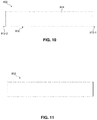
- FIG. 10 shows a front view of the example lens clip of FIG. 8 in accordance with an embodiment of the present disclosure.
- FIG. 11 shows a back view of the example lens clip of FIG. 8 in accordance with an embodiment of the present disclosure.
- FIG. 12 shows first and second lens clips disposed coaxially with each other in accordance with an embodiment of the present disclosure.
- FIG. 13 shows another perspective view of the first and second lens clips of FIG. 12 in accordance with an embodiment of the present disclosure.
- the present disclosure is generally directed to a lens clip that defines at least one mounting surface for coupling to and supporting an array of optical components, e.g., a laser diode and associated components, and an optical lens slot to receive and securely hold an array of optical lenses, e.g., focus lenses, at a predetermined position relative to the optical components to ensure nominal optical coupling.
- the optical lens slot includes dimensions that permit insertion of each optical lens into the same and restrict travel/displacement along one or more axis.
- assembly of an optical subassembly can include mounting of optical components such as laser assemblies to the mounting surface of the lens clip and then insertion of each focus lens within the lens slot for alignment purposes prior to, or after, insertion of the lens clip into a cavity of a TOSA housing.
- a lens clip consistent with the present disclosure can significantly reduce manufacturing complexity, manufacturing time per unit, misalignment errors, and increase active alignment tolerances compared to other approaches that that couple and align each laser and focus lens individually on a per-channel basis.
- each lens clip can include a lens slot capable of coupling to, for instance, four or more focus lenses. Therefore, after each focus lens and laser diode gets coupled together and aligned via the lens clip, alignment with other optical components such as an optical multiplexer within a TOSA housing can be achieved by simply shifting the lens clip along the X or Y axis rather than individually adjusting the position of each separate laser and lens.
- two or more lens clips and associated lenses and laser diodes can be assembled at least partially outside of a TOSA housing, and then disposed in the TOSA housing for mounting and optical alignment with multiplexer(s), transmit fiber(s), and so on.
- two or more lens clips can be utilized to increase channel counts to eight (8) or more, with at least a portion of assembly of the lens clip and associated components being optionally performed outside of the relatively space-constrained TOSA housing to advantageously reduce the risk of, for example, alignment errors and component damage.
- multi-channel TOSAs having lens clips consistent with the present disclosure can be assembled with 4, 8, 16, 24, 32 or N-channels in a manner that allows for optical alignment of multiple laser diodes and associated diodes in groups of two or more (depending on lens slot dimension, desired channel counts, etc.), which advantageously avoids the necessity of performing active test and re-alignment iterations for each individual laser and associated component.
- lens clips formed from transparent material e.g., capable of passing at least 50-80% of incident wavelengths and preferably 90-100% of incident UV wavelengths, significantly improves the structural integrity and reliability achieved through the use of UV-curing epoxies to attach focus lenses to a lens clip.
- an optical lens can be disposed in a manner that “bottoms out” (e.g., directly contacts a bottom surface defining the lens slot) such that epoxy gets disposed between adjacent optical lenses and/or the interstitial space between optical lenses and adjacent sidewalls of the lens slot while blocking/preventing all, or at least a majority, of epoxy from flowing beneath each lens.
- a lens clip consistent with the present disclosure may be utilized to align and mount optical lenses in receiver optical subassembly (ROSA) arrangements.
- channel wavelengths refer to the wavelengths associated with optical channels and may include a specified wavelength band around a center wavelength.
- the channel wavelengths may be defined by an International Telecommunication (ITU) standard such as the ITU-T dense wavelength division multiplexing (DWDM) grid. This disclosure is equally applicable to coarse wavelength division multiplexing (CWDM).
- the channel wavelengths are implemented in accordance with local area network (LAN) wavelength division multiplexing (WDM), which may also be referred to as LWDM.
- LAN local area network
- WDM wavelength division multiplexing
- Coupled refers to any connection, coupling, link or the like and “optically coupled” refers to coupling such that light from one element is imparted to another element. Such “coupled” devices are not necessarily directly connected to one another and may be separated by intermediate components or devices that may manipulate or modify such signals.
- directly optical coupling refers to an optical coupling via an optical path between two elements that does not include such intermediate components or devices, e.g., a mirror, waveguide, and so on, or bends/turns along the optical path between two elements.
- substantially refers to a degree of precision within acceptable tolerance that accounts for and reflects minor real-world variation due to material composition, material defects, and/or limitations/peculiarities in manufacturing processes. Such variation may therefore be said to achieve largely, but not necessarily wholly, the stated/nominal characteristic.
- a modifier is intended to include minor variation that can cause a deviation of up to and including ⁇ 5% from a particular stated quality/characteristic unless otherwise provided by the present disclosure.
- hermetic-sealed and hermetically-sealed may be used interchangeably and refer to a housing that releases a maximum of about 5*10 ⁇ 8 casec of filler gas.
- the filler gas may comprise an inert gas such as nitrogen, helium, argon, krypton, xenon, or various mixtures thereof, including a nitrogen-helium mix, a neon-helium mix, a krypton-helium mix, or a xenon-helium mix.
- the optical transceiver 100 includes a multi-channel transmitter optical subassembly (TOSA) arrangement 104 and a multi-channel receiver optical subassembly (ROSA) arrangement 106 coupled to a substrate 102 , which may also be referred to as an optical module substrate.
- the substrate 102 may comprise, for example, a printed circuit board (PCB) or PCB assembly (PCBA).
- PCB printed circuit board
- PCBA PCB assembly
- the substrate 102 may be configured to be “pluggable” for insertion into an optical transceiver cage 111 .
- the optical transceiver 100 transmits and receives eight (8) channels using eight different channel wavelengths ( ⁇ 1 . . . ⁇ 8) via the multi-channel TOSA arrangement 104 and the multi-channel ROSA arrangement 106 , respectively, and may be capable of transmission rates of at least about 25 Gbps per channel, and preferably 50 Gbps per channel.
- the optical transceiver 100 may also be capable of transmission distances of 2 km to at least about 10 km.
- the optical transceiver 100 may be used, for example, in internet data center applications or fiber to the home (FTTH) applications.
- FTTH fiber to the home
- the multi-channel TOSA arrangement 104 includes a TOSA housing 109 with a plurality of sidewalls that define a cavity.
- the cavity includes a plurality of laser arrangements 110 , a multiplexing device 125 , and a feedthrough device 116 disposed therein.
- the multi-channel TOSA arrangement 104 may be implemented as the multi-channel TOSA arrangement 204 of FIGS. 2-7 with at least one laser diode driver (LDD) disposed/mounted on the feedthrough device 116 , which will be discussed in greater detail below.
- LDD laser diode driver
- each laser arrangement of the plurality of laser arrangements 110 can be configured to transmit optical signals having different associated channel wavelengths.
- Each laser arrangement can include passive and/or active optical components such as a laser diode (LD), optical isolator, focus lens, monitor photodiode (MPD), and so on.
- LD laser diode
- MPD monitor photodiode
- the optical transceiver 100 includes a transmit connecting circuit 112 to provide electrical connections to the plurality of laser arrangements 110 within the housing 109 .
- the transmit connecting circuit 112 may be configured to receive driving signals (e.g., TX_D 1 to TX_D 8 ) from, for example, circuitry within the optical transceiver cage 111 .
- the housing 109 may be hermetically sealed to prevent ingress of foreign material, e.g., dust and debris.
- a plurality of transit (TX) traces 117 may be patterned on at least one surface of the substrate 102 and electrically coupled to a feedthrough device 116 of the TOSA housing 109 to bring the transmit connecting circuit 112 into electrical communication with the plurality of laser arrangements 110 , and thus, electrically interconnect the transmit connecting circuit 112 with the multi-channel TOSA arrangement 104 .
- the feedthrough device 116 may comprise, for instance, ceramic, metal, or any other suitable material.
- the multi-channel TOSA arrangement 104 may then receive driving signals (e.g., TX_D 1 to TX_D 8 ), and in response thereto, generate and launch multiplexed channel wavelengths on to an output waveguide 120 such as a transmit optical fiber.
- the generated multiplexed channel wavelengths may be combined based on a multiplexing device 125 such as an arrayed waveguide grating (AWG) that is configured to receive emitted channel wavelengths 126 from the plurality of laser arrangements 110 and output a signal carrying the multiplexed channel wavelengths on to the output waveguide 120 by way of optical fiber receptacle 122 .
- AMG arrayed waveguide grating
- the multi-channel ROSA arrangement 106 includes a demultiplexing device 124 , e.g., an arrayed waveguide grating (AWG), a photodiode (PD) array 128 , and amplification circuitry 130 , e.g., a transimpedance amplifier (TIA).
- An input port of the demultiplexing device 124 may be optically coupled with a receive waveguide 134 , e.g., an optical fiber, by way of an optical fiber receptacle 136 .
- An output port of the demultiplexing device 124 may be configured to output separated channel wavelengths on to the PD array 128 .
- the PD array 128 may then output proportional electrical signals to the TIA 130 , which then may be amplified and otherwise conditioned.
- the PD array 128 and the transimpedance amplifier 130 detect and convert optical signals into electrical data signals (RX_D 1 to RX_D 8 ) that are output via the receive connecting circuit 132 .
- the PD array 128 may then output electrical signals carrying a representation of the received channel wavelengths to a receive connecting circuit 132 by way of conductive traces 119 (which may be referred to as conductive paths).
- an example transceiver module 200 is shown consistent with an embodiment of the present disclosure.
- the example transceiver module 200 may be implemented as the optical transceiver 100 of FIG. 1 .
- the optical transceiver module 200 includes a configuration to send and receive eight (8) different channel wavelengths in order to provide transmission speeds up to and an in excess of 400 Gb/s, for instance.
- other channel configurations are within the scope of this disclosure and the embodiment of FIGS. 2-7 are not intended to limit the present disclosure.
- the optical transceiver module 200 includes a substrate 202 , multi-channel TOSA arrangement 204 , and a multi-channel ROSA arrangement 206 .
- the substrate 202 includes a first end 203 that extends to a second end 205 along a longitudinal axis 250 .
- a first and second mounting surface 245 , 246 disposed facing away from each other extend in parallel along the longitudinal axis 250 and define at least a portion of the substrate 202 .
- the substrate 202 may comprise, for example, a printed circuit board assembly (PCBA) or other suitable substrate material.
- the multi-channel ROSA arrangement 206 is coupled to and supported by the first mounting surface 245 at a position proximate the first end 203 of the substrate 202 .
- the multi-channel ROSA arrangement 206 can include on-board/integrated configuration as discussed and described in greater detail in the co-pending U.S. patent application Ser. No. 16/142,466 filed on Sep. 28, 2018 and entitled “Receiver Optical Subassembly (ROSA) Integrated On Printed Circuit Board Assembly,” the entirety of which is incorporated herein by reference.
- ROSA Receiveiver Optical Subassembly
- the multi-channel ROSA arrangement 206 includes a demultiplexing device 224 , e.g., an arrayed waveguide grating (AWG), with an input port 229 coupled to an optical coupling receptacle 236 by way of an intermediate waveguide 211 (e.g., an optical fiber).
- the demultiplexing device 224 further includes an output region aligned with a photodiode (PD) array 228 .
- the PD array 228 electrically couples to the first and second amplification chips 230 - 1 , 230 - 2 , e.g., transimpedance amplifiers (TIAs).
- TIAs transimpedance amplifiers
- a multiplexed optical signal received via the optical coupling receptacle 236 gets demultiplexed by the demultiplexer 224 .
- the demultiplexer 224 then outputs separated channel wavelengths on to corresponding photodiodes of the PD array 228 .
- the PD array 228 outputs an electrical current to the amplification circuitry 230 - 1 , 230 - 2 that is representative of the received and separated channel wavelengths.
- the amplification circuitry 230 - 1 , 230 - 2 then amplifies the electrical currents from the PD array 228 and outputs a signal to, for instance, a data bus via the receive connecting circuit 132 ( FIG. 1 ).
- the multi-channel TOSA arrangement 204 is coupled to the first end 203 of the substrate 202 and includes a plurality of laser arrangements and optical connectors for outputting a plurality of channel wavelengths, as discussed in greater detail below.
- the TOSA arrangement 204 may be edge mounted to the substrate 202 , as shown, although other suitable approaches are within the scope of this disclosure.
- the TOSA arrangement 204 includes a housing 209 , which may also be referred to as a TOSA housing.
- the housing 209 is defined by a plurality of sidewalls 256 - 1 to 256 - 6 that define a cavity 260 therebetween.
- the plurality of sidewalls 256 - 1 to 256 - 6 extend from a first end 261 to a second end 263 along the longitudinal axis 250 ( FIG. 2 ).
- the housing 209 may have other shapes and configurations and the provided example is not intended to be limiting.
- the TOSA arrangement 204 includes a feedthrough device 270 , a plurality of laser arrangements 274 , a multiplexing device 225 , an optical isolator chip 276 and an output port 279 .
- the feedthrough device 270 is disposed proximate the first end 261 of the housing 209 and extends at least partially into the cavity 260 .
- a first portion 232 - 1 of the feedthrough device 270 extends at least partially into the cavity 260 and a second portion 232 - 2 may extend from the cavity 260 towards the substrate 202 for coupling purposes (see FIG. 6 ).
- the feedthrough device 270 defines at least a portion of the cavity 260 .
- the feedthrough device 270 may comprise, for example, a suitably rigid non-metal material such as inorganic material such as a crystalline oxide, nitride or carbide material, which may be commonly referred to as ceramic. Some elements, such as carbon or silicon, may also be considered ceramics, and are also within the scope of this disclosure.
- each laser arrangement of the plurality of laser arrangements 274 includes a laser diode, a monitor photodiode, and a focus lens.
- Each laser arrangement also includes a corresponding LD driver (LDD) chip 242 mounted to the feedthrough device 270 .
- LDD LD driver
- each of the laser arrangements 274 can include a laser diode that is disposed at a substantially uniform distance of D 1 from an associated LDD chip, e.g., LDD chip 242 - 1 .
- LDD LD driver
- each of the plurality of laser diodes 274 and associated LDD chip e.g., LDD chip 242 - 1
- LDD chip 242 - 1 may be mounted in a manner that causes the same to extend directly up to the edge of their respective mounting surfaces.
- a relatively small air gap 285 also having an overall width of D 1 ) separates each of the laser diodes 274 and the associated LDD chips 242 .
- the proximity of each LD chip to an associated LDD chip can significantly shorten the length of an interconnect device between the same, such as a wire bond.
- the gap 285 can advantageously provide thermal isolation.
- a multiplexing device 225 is disposed at a midpoint within the cavity 260 .
- the multiplexing device 225 includes an input region 282 facing the first end 261 of the housing 209 , and more particularly the plurality of laser arrangements 274 .
- the input region 282 includes a plurality of input ports that are aligned to receive channel wavelengths from LDs along an associated light path.
- Each of the laser arrangements 274 may then emit associated channel wavelengths on a corresponding light path of a plurality of input light paths 286 that intersect with the input region 282 , which is more clearly shown in FIG. 5 .
- Each light path of the plurality of light paths 286 therefore extends from an emission surface of an associated LD through a focus lens, and then ultimately to the input region 282 .
- the multiplexing device 225 further includes an output port 284 that is disposed opposite the input region 282 such that the output port 284 faces the second end of the housing 209 .
- the output port 284 outputs a multiplexed signal along an output light path 290 .
- An optical isolator 276 proximate the second end 263 of the housing 209 includes an aperture 277 , by which the output light path 290 extends therethrough.
- the housing 209 includes an opening/aperture for coupling to an optical coupling receptacle 292 .
- the optical coupling receptacle 292 optically couples with the transmit optical coupling receptacle 222 by way of an intermediate fiber 294 . Accordingly, the multiplexing device 225 outputs a multiplexed optical signal for transmission via light path 290 .
- feedthrough device 270 may be defined by at least a first mounting surface 272 - 1 and a second mounting surface 272 - 2 . Although denoted as “first” and “second,” these designations are merely for purposes of clarity and are utilized simply to distinguish between the mounting surfaces 272 - 1 , 272 - 2 . To this end, either mounting surface may be referred to as a “first” or “second” surface.
- first and second mounting surfaces 272 - 1 , 272 - 2 may be formed integrally with the feedthrough device 270 as a single piece, e.g., allowing for direct coupling of components to the feedthrough device 270 .
- first and second mounting surfaces 272 - 1 , 272 - 2 may be provided by one or more submounts.
- the feedthrough device 270 advantageously provides mounting regions that facilitate such direct or indirect mounting and support of components.
- first and second mounting surfaces 272 - 1 , 272 - 2 may be substantially planar, such as shown, although the first and second mounting surfaces 272 - 1 , 272 - 2 are not limited in this respect and other embodiments are within the scope of this disclosure.
- the first and second mounting surfaces 272 - 1 , 272 - 1 extend in parallel relative to each other but are offset by a distance D (see FIG. 7 ) to provide a step structure or profile.
- the arrangement of the first and second mounting surfaces 272 - 1 , 272 - 2 may collectively provide a “stepped,” or multi-step mounting profile whereby the first and second mounting surfaces are adjoined by a surface 299 that extends substantially transverse to each and provides the offset distance D.
- the offset distance D may measure between 10 and 130 microns, and preferably 100 microns although other distances are within the scope of this disclosure.
- the first mounting surface 272 - 1 may be substantially coplanar with the first mounting surface 245 of the substrate 202 , or not, depending on a desired configuration. This may advantageously allow for electrical traces 233 disposed/patterned on the first mounting surface 272 - 1 to electrically couple with the substrate 202 via an interconnect device such as the bus bars 235 . Power and RF signals may be then provided to the TOSA arrangement, and more particularly, optical components disposed within the cavity 260 of the housing 9 . Accordingly, the first mounting surface 272 - 1 may also be referred to as a feedthrough mounting surface as at least a conductive portion of the same, e.g., the conductive traces patterned thereon, extends out from the cavity 260 of the housing 209 .
- the first mounting surface 272 - 1 includes a plurality of filtering capacitors 231 mounted thereon.
- the filtering capacitors 231 may be utilized when driving the plurality of laser arrangements to maintain signal integrity, e.g., by reducing noise, stabilizing the DC signal, for example.
- the second mounting surface 272 - 2 is disposed within the cavity 260 of the housing 209 and is disposed at the offset D from that of the first mounting surface 272 - 1 .
- the second mounting surface 272 - 2 may be accurately referred to as an internal mounting surface or a recessed mounting surface whereby the mounting surface 272 - 2 is fully within the cavity 260 of the housing 209 and below the first mounting surface 272 - 1 .
- the second mounting surface 272 - 2 be vertically offset from the laser diode (LD) submounts 280 - 1 , 280 - 2 such that the LD submounts 280 - 1 , 280 - 2 are below a horizontal plane extending from the second mounting surface 272 - 2 (see FIG. 7 ).
- the second mounting surface 272 - 2 may be substantially coplanar with and proximate to the LD submounts 280 - 1 , 280 - 2 .
- wire bonds 238 electrically couple the first and second LDD chips 242 - 1 , 242 - 2 to laser diodes of the plurality of laser arrangements 274 and are relatively short to advantageously reduce issues such as time of flight (TOF) and impedance mismatches, for example. Electrical interconnects other than wire bonds may be utilized, and the example embodiment of FIG. 6 should not be construed as limiting.
- the first and second LDD chips 242 - 1 , 242 - 2 can electrically couple to the plurality filtering capacitors 231 via wire bonds, for instance, although other types of interconnects are within the scope of this disclosure.
- the plurality of laser arrangements 274 electrically couple to the electric traces 239 of the second mounting surface 272 - 1 .
- the electrical traces 239 then couple to the traces 233 of the first mounting surface 272 - 1 , and ultimately circuitry of the substrate 202 , to complete an electrical circuit for RF and power signals.
- FIG. 7 shows additional aspects of the multi-channel TOSA arrangement 204 in accordance with an embodiment.
- the multiplexing device 225 and the plurality of laser arrangements 274 are supported by a thermoelectric cooler (TEC) 241 .
- the TEC 241 can provide one or more mounting surfaces to couple to active and/or passive optical components.
- the plurality of laser arrangements 274 mount/couple to the TEC 241 via the LD submount 266 , as shown, or can directly mount to the TEC 241 depending on a desired configuration.
- first and second LD chips 242 - 1 , 242 - 2 couple to and are supported by the second mounting surface 272 - 2 .
- the first and second LDD chips 242 - 1 , 242 - 2 are therefore in thermal communication with the housing 209 via feedthrough device 270 for heat dissipation purposes.
- an air gap 285 separates the first and second LDD chips 242 - 1 , 242 - 2 from the plurality of laser arrangements 274 .
- the plurality of laser arrangements 274 are in thermal communication with the housing 209 and/or the TEC 241 via a first thermal conduction path 267 to dissipate heat.
- the LDD chips 242 are in thermal communication with the housing 209 via a second thermal conduction path 268 provided at least in part by the feedthrough device 270 that extends from the mounting surfaces 272 - 1 , 272 - 2 to the metal housing 209 to dissipate heat.
- the first and second thermal conduction paths 267 , 268 are separate and distinct, which provides thermal isolation from each other as well as other components of the multi-channel TOSA arrangement 204 . Accordingly, less power may be consumed by the TEC 241 to ensure nominal performance of the multi-channel TOSA arrangement 204 based on the feedthrough device 270 dissipating heat communicated from the first and second LDD chips and/or filtering capacitors 231 .
- the multi-channel TOSA arrangement 204 receives an RF driving signal and power from the substrate 202 .
- the optical components such as the plurality of laser arrangements 274 receive the RF driving signal and power via the traces 233 , 239 .
- the plurality of laser arrangements 274 then modulate and launch channel wavelengths based on the received RF driving signal.
- the channel wavelengths are then received at the input region 282 of the multiplexing device 225 .
- the multiplexing device 225 then multiplexes the received channel wavelengths and outputs a multiplexed signal to the transmit optical coupling receptacle 222 by way of output port 284 and intermediate fiber 294 .
- the lens clip 802 includes a body 804 (or base 804 ), a lens slot 806 , at least one mounting surface 808 , and at least one mating surface 810 .
- the body 804 extends along a longitudinal axis 850 from a first end 812 - 1 to a second end 812 - 2 .
- the lens slot 806 extends length-wise along the body 804 and can securely hold a plurality of optical lenses in alignment relative to associated optical components, as discussed in greater detail below.
- the body 804 of the lens clip 802 may comprise, for example, a metal, metal alloy, or any other suitably rigid material.
- the body 804 of the lens clip 802 is at least partially transparent (e.g., at least 80% of incident wavelengths pass therethrough), for purposes of securely attaching focus lenses into the lens slot 806 using a UV-curing epoxy, for example.
- the body 804 may be formed as a single monolithic piece of material, or from multiple pieces depending on a desired configuration.
- the body 804 of the lens clip 802 includes at least first and second portions 814 - 1 , 814 - 2 .
- the first portion 814 - 1 extends substantially parallel with the longitudinal axis 850 and provides a step/shelf from the first end 812 - 1 to the second end 812 - 2 , with the step/shelf being defined at least in part by the at least one mounting surface 808 .
- the first portion 814 - 1 includes a height H 1 that provides the step/shelf for the at least one mounting surface 808 such that an imaginary line drawn extending along the surface defining the at least one mounting surface 808 is offset from a top surface 816 defined by the second portion 814 - 2 (See FIG. 9 ).
- the height H 1 of the first portion 814 - 1 is about 1 millimeter (mm), and preferably is 0.69 mm, although other heights are within the scope of this disclosure.
- the second portion 814 - 2 of the body 804 also extends substantially parallel with the longitudinal axis 850 and the first portion 814 - 1 .
- the second portion 814 - 2 defines a shoulder/step having a height H 2 that extends from the first end 812 - 1 to the second end 812 - 2 .
- the height H 2 of the second portion 814 - 2 is less than the height H 1 of the first portion 814 - 1 to provide the offset distance D 1 , as discussed above.
- height H 3 of the portion that defines the bottom of the lens slot 806 and that extends between the first and second portions 814 - 1 , 814 - 2 measures less than heights H 1 and H 2 .
- first and second portions 814 - 1 , 814 - 2 collectively define the lens slot 806 .
- a first sidewall 820 - 1 provided by the first portion 814 - 1 is disposed opposite a second sidewall 820 - 2 provided by the second portion 814 - 2 .
- the first and second sidewalls 820 - 1 , 820 - 2 extend substantially parallel with each other and have a gap extending therebetween, with the gap having a width of W 2 to provide the lens slot 806 .
- Bottom surface 820 - 3 extends substantially transverse relative to the first and second sidewalls 820 - 1 , 820 - 2 and adjoins the two.
- the lens slot 806 can have a U-shaped profile, such as shown in FIG. 9 , to generally correspond with the profile of the focus lenses.
- other shapes/profiles for the lens slot 806 are within the scope of this disclosure.
- the at least one mating surface 810 can be substantially flat, as shown, to couple to a sidewall of a subassembly housing.
- the at least one mating surface 810 may also allow for thermal coupling with the a heatsink, e.g., the subassembly housing, to promote thermal communication between optical components mounted to the at least one mounting surface 808 and the heatsink.
- the at least one mounting surface 808 can be substantially flat to couple to and support optical components such as laser arrangements (See FIG. 12 ).
- first and second lens clips 802 - 1 and 802 - 2 are disposed coaxially with each other such that a common longitudinal axis 850 extends therethrough.
- This coaxial arrangement is particularly well suited for use in multi-channel TOSAs, as is discussed in greater detail below.
- each of the first and second lens clips 802 - 1 , 802 - 2 include first and second arrays of focus lenses 840 - 1 , 840 - 2 , respectively.
- Each of the first and second arrays of focus lenses 840 - 1 , 840 - 2 couple to their respective lens clip via lens slots 806 - 1 , 806 - 2 , respectively.
- at least a portion of each focus lens gets inserted into an associated lens slot to securely hold the same in position relative to associated optical components. For instance, as shown in FIG.
- each laser arrangement attached to the first and second lens clips 802 - 1 , 802 - 2 can optically align with respective focus lenses by virtue of the mechanical alignment along the X, Y and Z axis provided by virtue of the lens slots dimension and location relative to the mounting surfaces of the first and second lens clips 802 - 1 , 802 - 2 that support the laser arrangements. As shown, this can result in each laser arrangement having an optical path extending therefrom that extends substantially parallel with each other.
- the lens slot is configured to securely hold and position each received optical lens in a collinear orientation such that the optical axis of each optical lens extend substantially parallel relative to each other.
- the first and second lens clips 840 - 1 , 840 - 2 may be implemented as the LD submounts 280 - 1 , 280 - 2 .
- a technician can optionally couple focus lenses and laser arrangements into each lens clip and perform alignment of the two separate and apart from the TOSA housing.
- a technician can then insert each lens clip into the housing in at least a partially-completed form such that the optical alignment of the laser arrangements with the input region of the multiplexer 225 is established by simply disposing each lens clip at a predetermined location, e.g., on a TEC or other submount, and measuring resulting output power.
- multi-channel TOSAs consistent with the present disclosure can be assembled with 4, 8, 16, 24, 32 or N channels in a manner that allows for optical alignment of multiple laser diodes and associated diodes in groups of two or more (depending on lens slot dimension, desired channel counts, etc.).
- a lens clip for use in an optical subassembly.
- the lens clip to mount and align an array of optical lenses with associated optical components, the lens clip comprising a body having a first end that extends to a second end, the body defining a lens slot that extends between the first and second end, and wherein the lens slot is configured to receive at least a portion of each optical lens of the array of optical lenses, a mating surface defined by the body to couple the lens clip to an optical subassembly housing, a mounting surface defined by the body, the mounting surface disposed along the lens slot and configured to couple to and support a plurality of optical components, and wherein the lens slot is configured to optically align each optical lens of the array of optical lenses with an associated optical component mounted to the at least one mounting surface.
- a transmitter optical subassembly (TOSA) arrangement comprising a housing having a plurality of sidewalls that define a cavity therebetween, a first lens clip disposed in the cavity, the first lens clip defining a mating surface to couple to the housing and a lens slot to receive and couple to a plurality of focus lenses, an array of focus lenses disposed in the first lens slot, and a first plurality of laser arrangements disposed on a surface of the first lens clip, each laser arrangement of the first plurality of laser arrangements having a laser diode optically aligned with an associated focus lens of the first array of focus lenses.
- a method for assembling an optical subassembly comprising mounting a plurality of laser assemblies to a mounting surface provided by a lens clip, inserting a plurality of optical lenses into a lens array slot defined by the lens clip and aligning each optical lens of the plurality of optical lenses with an associated laser assembly of the plurality of laser assemblies, mounting the lens clip within a cavity of a transmitter optical subassembly (TOSA) housing, and aligning the lens clip with an arrayed waveguide grating (AWG) within the housing.
- TOSA transmitter optical subassembly
Landscapes
- Physics & Mathematics (AREA)
- Optics & Photonics (AREA)
- General Physics & Mathematics (AREA)
- Electromagnetism (AREA)
- Engineering & Computer Science (AREA)
- Computer Networks & Wireless Communication (AREA)
- Signal Processing (AREA)
- Optical Couplings Of Light Guides (AREA)
- Semiconductor Lasers (AREA)
Abstract
Description
Claims (11)
Priority Applications (2)
| Application Number | Priority Date | Filing Date | Title |
|---|---|---|---|
| US16/514,580 US11221460B2 (en) | 2019-07-17 | 2019-07-17 | Lens clip for coupling and optical alignment of an optical lens array and an optical subassembly module implementing same |
| CN202010650708.7A CN112241055B (en) | 2019-07-17 | 2020-07-08 | Lens holder for coupling and optically aligning an optical lens array and optical subassembly module for implementing the same |
Applications Claiming Priority (1)
| Application Number | Priority Date | Filing Date | Title |
|---|---|---|---|
| US16/514,580 US11221460B2 (en) | 2019-07-17 | 2019-07-17 | Lens clip for coupling and optical alignment of an optical lens array and an optical subassembly module implementing same |
Publications (2)
| Publication Number | Publication Date |
|---|---|
| US20210018716A1 US20210018716A1 (en) | 2021-01-21 |
| US11221460B2 true US11221460B2 (en) | 2022-01-11 |
Family
ID=74170591
Family Applications (1)
| Application Number | Title | Priority Date | Filing Date |
|---|---|---|---|
| US16/514,580 Active 2040-02-13 US11221460B2 (en) | 2019-07-17 | 2019-07-17 | Lens clip for coupling and optical alignment of an optical lens array and an optical subassembly module implementing same |
Country Status (2)
| Country | Link |
|---|---|
| US (1) | US11221460B2 (en) |
| CN (1) | CN112241055B (en) |
Citations (4)
| Publication number | Priority date | Publication date | Assignee | Title |
|---|---|---|---|---|
| US5412509A (en) * | 1992-07-21 | 1995-05-02 | Rohm Co., Ltd. | Light source unit incorporating light emitting device and optical device |
| US20130057834A1 (en) * | 2011-09-07 | 2013-03-07 | Casio Computer Co., Ltd. | Lens array, light source device, projector and light source device fabrication method |
| US8562141B2 (en) * | 2011-03-28 | 2013-10-22 | Casio Computer Co., Ltd. | Light-source apparatus and projector |
| US20190129196A1 (en) * | 2013-05-10 | 2019-05-02 | North Inc. | Projection device |
Family Cites Families (2)
| Publication number | Priority date | Publication date | Assignee | Title |
|---|---|---|---|---|
| DE19643462A1 (en) * | 1996-10-22 | 1998-04-23 | Hella Kg Hueck & Co | Headlights for vehicles |
| CN102169214A (en) * | 2011-05-03 | 2011-08-31 | 苏州旭创科技有限公司 | Optical transceiver component for parallel transmission |
-
2019
- 2019-07-17 US US16/514,580 patent/US11221460B2/en active Active
-
2020
- 2020-07-08 CN CN202010650708.7A patent/CN112241055B/en active Active
Patent Citations (5)
| Publication number | Priority date | Publication date | Assignee | Title |
|---|---|---|---|---|
| US5412509A (en) * | 1992-07-21 | 1995-05-02 | Rohm Co., Ltd. | Light source unit incorporating light emitting device and optical device |
| US8562141B2 (en) * | 2011-03-28 | 2013-10-22 | Casio Computer Co., Ltd. | Light-source apparatus and projector |
| US20130057834A1 (en) * | 2011-09-07 | 2013-03-07 | Casio Computer Co., Ltd. | Lens array, light source device, projector and light source device fabrication method |
| US9061378B2 (en) * | 2011-09-07 | 2015-06-23 | Casio Computer Co., Ltd. | Lens array, light source device, projector and light source device fabrication method |
| US20190129196A1 (en) * | 2013-05-10 | 2019-05-02 | North Inc. | Projection device |
Also Published As
| Publication number | Publication date |
|---|---|
| CN112241055B (en) | 2023-10-24 |
| US20210018716A1 (en) | 2021-01-21 |
| CN112241055A (en) | 2021-01-19 |
Similar Documents
| Publication | Publication Date | Title |
|---|---|---|
| US10073229B2 (en) | Transmitter optical subassembly (TOSA) module with integrated welding member for use in optical transmitters or transceivers | |
| US10509184B2 (en) | Welding assembly for coupling a transmitter optical subassembly (TOSA) module to an optical transmitter or transceiver | |
| US10698168B1 (en) | Printed circuit board assembly (PCBA) with integrated mounting structure to align and couple to transmitter optical assembly (TOSA) modules | |
| US10884201B2 (en) | Receptacle configuration to support on-board receiver optical subassembly (ROSA) | |
| US10950651B2 (en) | Photodiode (PD) array with integrated back-side lenses and a multi-channel transceiver module implementing same | |
| US20200328814A1 (en) | Optical packaging and designs for optical transceivers | |
| US10833775B1 (en) | Techniques for magnetic shielding of an optical isolator to maintain nominal magnetic flux density and a transmitter or transceiver system implementing same | |
| CN111221085B (en) | Optical isolator array for use in optical subassembly modules | |
| US10714890B1 (en) | Transmitter optical subassembly arrangement with vertically-mounted monitor photodiodes | |
| CN111338034B (en) | Light emission sub-assembly with laser diode driver circuit mounted in feedthrough means of light emission sub-assembly housing | |
| JP7030417B2 (en) | Optical subassemblies, optical modules, and optical transmitters | |
| US11411650B2 (en) | Component bridge for increasing mounting surface area on feedthrough device and an optical subassembly implementing same | |
| US10928600B2 (en) | Transmitter optical subassembly (TOSA) with laser diode driver (LDD) circuitry mounted to feedthrough of TOSA housing | |
| US11221460B2 (en) | Lens clip for coupling and optical alignment of an optical lens array and an optical subassembly module implementing same | |
| CN111175911B (en) | Optical alignment of optical lenses, optical sub-assembly module for coupling lens clips, optical lenses, and optical sub-assembly module for implementing same | |
| US10983291B2 (en) | Holder element with integrated optical arrangement to offset an output light path | |
| CN111258008A (en) | Light emission subassembly configuration with vertically mounted monitor photodiode | |
| CN114069381B (en) | Thermal management technology in optical subassembly module and heating device for laser diode temperature control | |
| US11177887B2 (en) | Substrate with stepped profile for mounting transmitter optical subassemblies and an optical transmitter or transceiver implementing same | |
| CN112713127B (en) | Light emission sub-assembly with laser diode driver circuit mounted to feed device of light emission sub-assembly housing | |
| US20220045478A1 (en) | Techniques for thermal management within optical subassembly modules |
Legal Events
| Date | Code | Title | Description |
|---|---|---|---|
| AS | Assignment |
Owner name: APPLIED OPTOELECTRONICS, INC., TEXAS Free format text: ASSIGNMENT OF ASSIGNORS INTEREST;ASSIGNORS:HO, I-LUNG;WANG, HSIU-CHE;LI, QIN;REEL/FRAME:049781/0430 Effective date: 20190715 |
|
| FEPP | Fee payment procedure |
Free format text: ENTITY STATUS SET TO UNDISCOUNTED (ORIGINAL EVENT CODE: BIG.); ENTITY STATUS OF PATENT OWNER: LARGE ENTITY |
|
| STPP | Information on status: patent application and granting procedure in general |
Free format text: NON FINAL ACTION MAILED |
|
| STPP | Information on status: patent application and granting procedure in general |
Free format text: RESPONSE TO NON-FINAL OFFICE ACTION ENTERED AND FORWARDED TO EXAMINER |
|
| STPP | Information on status: patent application and granting procedure in general |
Free format text: NOTICE OF ALLOWANCE MAILED -- APPLICATION RECEIVED IN OFFICE OF PUBLICATIONS |
|
| STPP | Information on status: patent application and granting procedure in general |
Free format text: PUBLICATIONS -- ISSUE FEE PAYMENT VERIFIED |
|
| STCF | Information on status: patent grant |
Free format text: PATENTED CASE |
|
| AS | Assignment |
Owner name: CIT NORTHBRIDGE CREDIT LLC, NEW YORK Free format text: PATENT SECURITY AGREEMENT;ASSIGNOR:APPLIED OPTOELECTRONICS, INC.;REEL/FRAME:062003/0523 Effective date: 20221116 |
|
| AS | Assignment |
Owner name: APPLIED OPTOELECTRONICS, INC., TEXAS Free format text: TERMINATION AND RELEASE OF SECURITY INTEREST IN PATENTS;ASSIGNOR:CIT NORTHBRIDGE CREDIT LLC;REEL/FRAME:065630/0906 Effective date: 20231117 |