US11213976B2 - Imprinting apparatus - Google Patents
Imprinting apparatus Download PDFInfo
- Publication number
- US11213976B2 US11213976B2 US15/847,150 US201715847150A US11213976B2 US 11213976 B2 US11213976 B2 US 11213976B2 US 201715847150 A US201715847150 A US 201715847150A US 11213976 B2 US11213976 B2 US 11213976B2
- Authority
- US
- United States
- Prior art keywords
- silicon
- molecule
- working stamp
- master
- group
- Prior art date
- Legal status (The legal status is an assumption and is not a legal conclusion. Google has not performed a legal analysis and makes no representation as to the accuracy of the status listed.)
- Active, expires
Links
- 239000000463 material Substances 0.000 claims abstract description 132
- 238000000034 method Methods 0.000 claims abstract description 101
- XUIMIQQOPSSXEZ-UHFFFAOYSA-N Silicon Chemical compound [Si] XUIMIQQOPSSXEZ-UHFFFAOYSA-N 0.000 claims abstract description 89
- 229910052710 silicon Inorganic materials 0.000 claims abstract description 89
- 239000010703 silicon Substances 0.000 claims abstract description 89
- 239000000203 mixture Substances 0.000 claims abstract description 68
- 238000009472 formulation Methods 0.000 claims abstract description 55
- 238000000151 deposition Methods 0.000 claims abstract description 34
- 239000002904 solvent Substances 0.000 claims abstract description 27
- BLRPTPMANUNPDV-UHFFFAOYSA-N Silane Chemical group [SiH4] BLRPTPMANUNPDV-UHFFFAOYSA-N 0.000 claims abstract description 22
- 229920000642 polymer Polymers 0.000 claims description 32
- 239000011347 resin Substances 0.000 claims description 31
- 229920005989 resin Polymers 0.000 claims description 31
- 238000012163 sequencing technique Methods 0.000 claims description 25
- WYURNTSHIVDZCO-UHFFFAOYSA-N Tetrahydrofuran Chemical group C1CCOC1 WYURNTSHIVDZCO-UHFFFAOYSA-N 0.000 claims description 18
- 239000011248 coating agent Substances 0.000 claims description 14
- 238000000576 coating method Methods 0.000 claims description 14
- 239000000178 monomer Substances 0.000 claims description 13
- SOGFHWHHBILCSX-UHFFFAOYSA-J prop-2-enoate silicon(4+) Chemical compound [Si+4].[O-]C(=O)C=C.[O-]C(=O)C=C.[O-]C(=O)C=C.[O-]C(=O)C=C SOGFHWHHBILCSX-UHFFFAOYSA-J 0.000 claims description 13
- 230000010076 replication Effects 0.000 claims description 10
- 125000004400 (C1-C12) alkyl group Chemical group 0.000 claims description 9
- 125000004169 (C1-C6) alkyl group Chemical group 0.000 claims description 9
- YXFVVABEGXRONW-UHFFFAOYSA-N Toluene Chemical compound CC1=CC=CC=C1 YXFVVABEGXRONW-UHFFFAOYSA-N 0.000 claims description 9
- YLQBMQCUIZJEEH-UHFFFAOYSA-N tetrahydrofuran Natural products C=1C=COC=1 YLQBMQCUIZJEEH-UHFFFAOYSA-N 0.000 claims description 9
- 229910052731 fluorine Inorganic materials 0.000 claims description 8
- 239000011737 fluorine Substances 0.000 claims description 8
- 125000000217 alkyl group Chemical group 0.000 claims description 7
- 238000009835 boiling Methods 0.000 claims description 7
- IUMSDRXLFWAGNT-UHFFFAOYSA-N Dodecamethylcyclohexasiloxane Chemical compound C[Si]1(C)O[Si](C)(C)O[Si](C)(C)O[Si](C)(C)O[Si](C)(C)O[Si](C)(C)O1 IUMSDRXLFWAGNT-UHFFFAOYSA-N 0.000 claims description 6
- 230000003321 amplification Effects 0.000 claims description 6
- DDJSWKLBKSLAAZ-UHFFFAOYSA-N cyclotetrasiloxane Chemical compound O1[SiH2]O[SiH2]O[SiH2]O[SiH2]1 DDJSWKLBKSLAAZ-UHFFFAOYSA-N 0.000 claims description 6
- 125000001495 ethyl group Chemical group [H]C([H])([H])C([H])([H])* 0.000 claims description 6
- 238000003199 nucleic acid amplification method Methods 0.000 claims description 6
- 238000004528 spin coating Methods 0.000 claims description 6
- 125000000547 substituted alkyl group Chemical group 0.000 claims description 6
- 125000000852 azido group Chemical group *N=[N+]=[N-] 0.000 claims description 5
- 238000004140 cleaning Methods 0.000 claims description 5
- 230000008021 deposition Effects 0.000 claims description 5
- 238000001459 lithography Methods 0.000 claims description 5
- 125000002496 methyl group Chemical group [H]C([H])([H])* 0.000 claims description 4
- QQQSFSZALRVCSZ-UHFFFAOYSA-N triethoxysilane Chemical compound CCO[SiH](OCC)OCC QQQSFSZALRVCSZ-UHFFFAOYSA-N 0.000 claims description 4
- XMSXQFUHVRWGNA-UHFFFAOYSA-N Decamethylcyclopentasiloxane Chemical compound C[Si]1(C)O[Si](C)(C)O[Si](C)(C)O[Si](C)(C)O[Si](C)(C)O1 XMSXQFUHVRWGNA-UHFFFAOYSA-N 0.000 claims description 3
- 125000003178 carboxy group Chemical class [H]OC(*)=O 0.000 claims description 3
- OAKJQQAXSVQMHS-UHFFFAOYSA-N hydrazine Substances NN OAKJQQAXSVQMHS-UHFFFAOYSA-N 0.000 claims description 3
- 150000002429 hydrazines Chemical class 0.000 claims description 3
- 150000007857 hydrazones Chemical class 0.000 claims description 3
- 125000004356 hydroxy functional group Chemical class O* 0.000 claims description 3
- SQDFHQJTAWCFIB-UHFFFAOYSA-N n-methylidenehydroxylamine Chemical compound ON=C SQDFHQJTAWCFIB-UHFFFAOYSA-N 0.000 claims description 3
- 150000002825 nitriles Chemical class 0.000 claims description 3
- 125000002924 primary amino group Chemical group [H]N([H])* 0.000 claims description 3
- 125000005017 substituted alkenyl group Chemical group 0.000 claims description 3
- 150000004905 tetrazines Chemical class 0.000 claims description 3
- 150000003536 tetrazoles Chemical class 0.000 claims description 3
- 150000003573 thiols Chemical class 0.000 claims description 3
- DENFJSAFJTVPJR-UHFFFAOYSA-N triethoxy(ethyl)silane Chemical group CCO[Si](CC)(OCC)OCC DENFJSAFJTVPJR-UHFFFAOYSA-N 0.000 claims description 3
- 125000001436 propyl group Chemical group [H]C([*])([H])C([H])([H])C([H])([H])[H] 0.000 claims description 2
- YUYCVXFAYWRXLS-UHFFFAOYSA-N trimethoxysilane Chemical compound CO[SiH](OC)OC YUYCVXFAYWRXLS-UHFFFAOYSA-N 0.000 claims description 2
- PXGOKWXKJXAPGV-UHFFFAOYSA-N Fluorine Chemical compound FF PXGOKWXKJXAPGV-UHFFFAOYSA-N 0.000 claims 3
- 239000010410 layer Substances 0.000 description 42
- 230000000052 comparative effect Effects 0.000 description 40
- 239000000758 substrate Substances 0.000 description 37
- 230000008569 process Effects 0.000 description 27
- 238000001127 nanoimprint lithography Methods 0.000 description 20
- -1 for example Substances 0.000 description 18
- 238000001723 curing Methods 0.000 description 16
- 238000004519 manufacturing process Methods 0.000 description 16
- 150000001875 compounds Chemical class 0.000 description 14
- 239000000499 gel Substances 0.000 description 14
- 230000003746 surface roughness Effects 0.000 description 14
- VYPSYNLAJGMNEJ-UHFFFAOYSA-N silicon dioxide Inorganic materials O=[Si]=O VYPSYNLAJGMNEJ-UHFFFAOYSA-N 0.000 description 11
- 235000012431 wafers Nutrition 0.000 description 9
- 238000004630 atomic force microscopy Methods 0.000 description 8
- 229920001577 copolymer Polymers 0.000 description 7
- 239000012634 fragment Substances 0.000 description 7
- 125000000524 functional group Chemical group 0.000 description 7
- 230000002068 genetic effect Effects 0.000 description 7
- 238000001878 scanning electron micrograph Methods 0.000 description 7
- 238000009736 wetting Methods 0.000 description 7
- RHBZBDOMPAUCTL-UHFFFAOYSA-N CCC[Si]1(C)O[Si](C)(CCO(CC)[SiH](OCC)OCC)O[Si](C)(CCO(CC)[SiH](OCC)OCC)O[Si](C)(CC[Si](OCC)(OCC)OCC)O1 Chemical compound CCC[Si]1(C)O[Si](C)(CCO(CC)[SiH](OCC)OCC)O[Si](C)(CCO(CC)[SiH](OCC)OCC)O[Si](C)(CC[Si](OCC)(OCC)OCC)O1 RHBZBDOMPAUCTL-UHFFFAOYSA-N 0.000 description 6
- 108020004414 DNA Proteins 0.000 description 6
- 102000053602 DNA Human genes 0.000 description 6
- 238000003848 UV Light-Curing Methods 0.000 description 6
- 239000011521 glass Substances 0.000 description 6
- 239000000126 substance Substances 0.000 description 6
- 238000012360 testing method Methods 0.000 description 6
- XLYOFNOQVPJJNP-UHFFFAOYSA-N water Substances O XLYOFNOQVPJJNP-UHFFFAOYSA-N 0.000 description 6
- HRPVXLWXLXDGHG-UHFFFAOYSA-N Acrylamide Chemical compound NC(=O)C=C HRPVXLWXLXDGHG-UHFFFAOYSA-N 0.000 description 5
- YCKRFDGAMUMZLT-UHFFFAOYSA-N Fluorine atom Chemical compound [F] YCKRFDGAMUMZLT-UHFFFAOYSA-N 0.000 description 5
- 238000003491 array Methods 0.000 description 5
- 229910000077 silane Inorganic materials 0.000 description 5
- 229920000089 Cyclic olefin copolymer Polymers 0.000 description 4
- 239000000853 adhesive Substances 0.000 description 4
- 230000001070 adhesive effect Effects 0.000 description 4
- 125000003277 amino group Chemical group 0.000 description 4
- 238000005229 chemical vapour deposition Methods 0.000 description 4
- 238000003618 dip coating Methods 0.000 description 4
- 239000007788 liquid Substances 0.000 description 4
- 108090000623 proteins and genes Proteins 0.000 description 4
- 239000000523 sample Substances 0.000 description 4
- 239000000377 silicon dioxide Substances 0.000 description 4
- 239000002210 silicon-based material Substances 0.000 description 4
- 150000003384 small molecules Chemical class 0.000 description 4
- 230000003068 static effect Effects 0.000 description 4
- 238000001029 thermal curing Methods 0.000 description 4
- 238000012546 transfer Methods 0.000 description 4
- 0 **CC(=O)NCNC(=O)C(C)C([1*])C(C(N)=O)C([5*])C Chemical compound **CC(=O)NCNC(=O)C(C)C([1*])C(C(N)=O)C([5*])C 0.000 description 3
- 238000007598 dipping method Methods 0.000 description 3
- CWAFVXWRGIEBPL-UHFFFAOYSA-N ethoxysilane Chemical group CCO[SiH3] CWAFVXWRGIEBPL-UHFFFAOYSA-N 0.000 description 3
- 229910052751 metal Inorganic materials 0.000 description 3
- 239000002184 metal Substances 0.000 description 3
- 239000002086 nanomaterial Substances 0.000 description 3
- 229920003229 poly(methyl methacrylate) Polymers 0.000 description 3
- 229920000915 polyvinyl chloride Polymers 0.000 description 3
- 239000004800 polyvinyl chloride Substances 0.000 description 3
- 230000005855 radiation Effects 0.000 description 3
- 229920002477 rna polymer Polymers 0.000 description 3
- 235000012239 silicon dioxide Nutrition 0.000 description 3
- 125000006850 spacer group Chemical group 0.000 description 3
- 238000005507 spraying Methods 0.000 description 3
- 230000008961 swelling Effects 0.000 description 3
- WSHQCIQLWZPNQZ-UHFFFAOYSA-N triethoxy-[2-[2,4,6,8-tetramethyl-4,6,8-tris(2-triethoxysilylethyl)-1,3,5,7,2,4,6,8-tetraoxatetrasilocan-2-yl]ethyl]silane Chemical compound CCO[Si](OCC)(OCC)CC[Si]1(C)O[Si](C)(CC[Si](OCC)(OCC)OCC)O[Si](C)(CC[Si](OCC)(OCC)OCC)O[Si](C)(CC[Si](OCC)(OCC)OCC)O1 WSHQCIQLWZPNQZ-UHFFFAOYSA-N 0.000 description 3
- 229910052727 yttrium Inorganic materials 0.000 description 3
- SMZOUWXMTYCWNB-UHFFFAOYSA-N 2-(2-methoxy-5-methylphenyl)ethanamine Chemical compound COC1=CC=C(C)C=C1CCN SMZOUWXMTYCWNB-UHFFFAOYSA-N 0.000 description 2
- NIXOWILDQLNWCW-UHFFFAOYSA-N 2-Propenoic acid Natural products OC(=O)C=C NIXOWILDQLNWCW-UHFFFAOYSA-N 0.000 description 2
- NIXOWILDQLNWCW-UHFFFAOYSA-M Acrylate Chemical compound [O-]C(=O)C=C NIXOWILDQLNWCW-UHFFFAOYSA-M 0.000 description 2
- JBRZTFJDHDCESZ-UHFFFAOYSA-N AsGa Chemical compound [As]#[Ga] JBRZTFJDHDCESZ-UHFFFAOYSA-N 0.000 description 2
- PXHVJJICTQNCMI-UHFFFAOYSA-N Nickel Chemical compound [Ni] PXHVJJICTQNCMI-UHFFFAOYSA-N 0.000 description 2
- 239000004642 Polyimide Substances 0.000 description 2
- 239000004793 Polystyrene Substances 0.000 description 2
- GOOHAUXETOMSMM-UHFFFAOYSA-N Propylene oxide Chemical compound CC1CO1 GOOHAUXETOMSMM-UHFFFAOYSA-N 0.000 description 2
- 108020004682 Single-Stranded DNA Proteins 0.000 description 2
- PPBRXRYQALVLMV-UHFFFAOYSA-N Styrene Chemical compound C=CC1=CC=CC=C1 PPBRXRYQALVLMV-UHFFFAOYSA-N 0.000 description 2
- 239000012491 analyte Substances 0.000 description 2
- 238000004380 ashing Methods 0.000 description 2
- 230000008901 benefit Effects 0.000 description 2
- 229920001222 biopolymer Polymers 0.000 description 2
- 239000000919 ceramic Substances 0.000 description 2
- 125000003636 chemical group Chemical group 0.000 description 2
- 239000003153 chemical reaction reagent Substances 0.000 description 2
- KOPOQZFJUQMUML-UHFFFAOYSA-N chlorosilane Chemical compound Cl[SiH3] KOPOQZFJUQMUML-UHFFFAOYSA-N 0.000 description 2
- 229920006037 cross link polymer Polymers 0.000 description 2
- 238000005516 engineering process Methods 0.000 description 2
- 238000011156 evaluation Methods 0.000 description 2
- 238000007306 functionalization reaction Methods 0.000 description 2
- 238000005227 gel permeation chromatography Methods 0.000 description 2
- 238000013007 heat curing Methods 0.000 description 2
- AMGQUBHHOARCQH-UHFFFAOYSA-N indium;oxotin Chemical compound [In].[Sn]=O AMGQUBHHOARCQH-UHFFFAOYSA-N 0.000 description 2
- ARYZCSRUUPFYMY-UHFFFAOYSA-N methoxysilane Chemical compound CO[SiH3] ARYZCSRUUPFYMY-UHFFFAOYSA-N 0.000 description 2
- 239000002105 nanoparticle Substances 0.000 description 2
- 102000039446 nucleic acids Human genes 0.000 description 2
- 108020004707 nucleic acids Proteins 0.000 description 2
- 150000007523 nucleic acids Chemical class 0.000 description 2
- 239000002773 nucleotide Substances 0.000 description 2
- 125000003729 nucleotide group Chemical group 0.000 description 2
- 125000004430 oxygen atom Chemical group O* 0.000 description 2
- 238000000059 patterning Methods 0.000 description 2
- 238000005498 polishing Methods 0.000 description 2
- 229920002401 polyacrylamide Polymers 0.000 description 2
- 229920000139 polyethylene terephthalate Polymers 0.000 description 2
- 239000005020 polyethylene terephthalate Substances 0.000 description 2
- 229920001721 polyimide Polymers 0.000 description 2
- 238000006116 polymerization reaction Methods 0.000 description 2
- 239000004926 polymethyl methacrylate Substances 0.000 description 2
- 229920002223 polystyrene Polymers 0.000 description 2
- 229920001343 polytetrafluoroethylene Polymers 0.000 description 2
- 239000004810 polytetrafluoroethylene Substances 0.000 description 2
- 238000012545 processing Methods 0.000 description 2
- 102000004169 proteins and genes Human genes 0.000 description 2
- 239000010453 quartz Substances 0.000 description 2
- 238000005096 rolling process Methods 0.000 description 2
- LIVNPJMFVYWSIS-UHFFFAOYSA-N silicon monoxide Inorganic materials [Si-]#[O+] LIVNPJMFVYWSIS-UHFFFAOYSA-N 0.000 description 2
- 230000009897 systematic effect Effects 0.000 description 2
- WOEYOUBBHRYDLG-UHFFFAOYSA-N 2-azidoacetamide Chemical group NC(=O)CN=[N+]=[N-] WOEYOUBBHRYDLG-UHFFFAOYSA-N 0.000 description 1
- 229920000936 Agarose Polymers 0.000 description 1
- CVUUKDCXXXZJGR-UHFFFAOYSA-N CCC(CC(C)C(=O)NCCCCCNC(=O)CN=[N+]=[N-])C(N)=O Chemical compound CCC(CC(C)C(=O)NCCCCCNC(=O)CN=[N+]=[N-])C(N)=O CVUUKDCXXXZJGR-UHFFFAOYSA-N 0.000 description 1
- OKTJSMMVPCPJKN-UHFFFAOYSA-N Carbon Chemical compound [C] OKTJSMMVPCPJKN-UHFFFAOYSA-N 0.000 description 1
- 238000001712 DNA sequencing Methods 0.000 description 1
- 108010010803 Gelatin Proteins 0.000 description 1
- GPXJNWSHGFTCBW-UHFFFAOYSA-N Indium phosphide Chemical compound [In]#P GPXJNWSHGFTCBW-UHFFFAOYSA-N 0.000 description 1
- 108091028043 Nucleic acid sequence Proteins 0.000 description 1
- 239000004698 Polyethylene Substances 0.000 description 1
- 239000002202 Polyethylene glycol Chemical group 0.000 description 1
- 239000004743 Polypropylene Substances 0.000 description 1
- 108020004518 RNA Probes Proteins 0.000 description 1
- 239000003391 RNA probe Substances 0.000 description 1
- 229910018557 Si O Inorganic materials 0.000 description 1
- 229910052581 Si3N4 Inorganic materials 0.000 description 1
- 229920006362 Teflon® Polymers 0.000 description 1
- GWEVSGVZZGPLCZ-UHFFFAOYSA-N Titan oxide Chemical compound O=[Ti]=O GWEVSGVZZGPLCZ-UHFFFAOYSA-N 0.000 description 1
- 229920006397 acrylic thermoplastic Polymers 0.000 description 1
- HFBMWMNUJJDEQZ-UHFFFAOYSA-N acryloyl chloride Chemical compound ClC(=O)C=C HFBMWMNUJJDEQZ-UHFFFAOYSA-N 0.000 description 1
- 230000004913 activation Effects 0.000 description 1
- 150000001336 alkenes Chemical class 0.000 description 1
- 125000003342 alkenyl group Chemical group 0.000 description 1
- 150000001345 alkine derivatives Chemical class 0.000 description 1
- 125000003545 alkoxy group Chemical group 0.000 description 1
- 125000000304 alkynyl group Chemical group 0.000 description 1
- 229910052782 aluminium Inorganic materials 0.000 description 1
- XAGFODPZIPBFFR-UHFFFAOYSA-N aluminium Chemical compound [Al] XAGFODPZIPBFFR-UHFFFAOYSA-N 0.000 description 1
- 238000004458 analytical method Methods 0.000 description 1
- 238000010560 atom transfer radical polymerization reaction Methods 0.000 description 1
- 238000000089 atomic force micrograph Methods 0.000 description 1
- 238000003766 bioinformatics method Methods 0.000 description 1
- 229910052799 carbon Inorganic materials 0.000 description 1
- 125000002915 carbonyl group Chemical group [*:2]C([*:1])=O 0.000 description 1
- 125000002843 carboxylic acid group Chemical group 0.000 description 1
- 230000015556 catabolic process Effects 0.000 description 1
- 230000008859 change Effects 0.000 description 1
- 238000006243 chemical reaction Methods 0.000 description 1
- 229910052681 coesite Inorganic materials 0.000 description 1
- 230000000295 complement effect Effects 0.000 description 1
- 239000002131 composite material Substances 0.000 description 1
- 229910052906 cristobalite Inorganic materials 0.000 description 1
- 238000004132 cross linking Methods 0.000 description 1
- 238000006352 cycloaddition reaction Methods 0.000 description 1
- 125000000392 cycloalkenyl group Chemical group 0.000 description 1
- 230000007547 defect Effects 0.000 description 1
- 238000006731 degradation reaction Methods 0.000 description 1
- 238000001514 detection method Methods 0.000 description 1
- 239000000539 dimer Substances 0.000 description 1
- 201000010099 disease Diseases 0.000 description 1
- 208000037265 diseases, disorders, signs and symptoms Diseases 0.000 description 1
- 238000004049 embossing Methods 0.000 description 1
- 125000003700 epoxy group Chemical group 0.000 description 1
- 125000004185 ester group Chemical group 0.000 description 1
- 238000005530 etching Methods 0.000 description 1
- KCWYOFZQRFCIIE-UHFFFAOYSA-N ethylsilane Chemical compound CC[SiH3] KCWYOFZQRFCIIE-UHFFFAOYSA-N 0.000 description 1
- 239000012530 fluid Substances 0.000 description 1
- 239000013022 formulation composition Substances 0.000 description 1
- 239000005350 fused silica glass Substances 0.000 description 1
- 239000008273 gelatin Substances 0.000 description 1
- 229920000159 gelatin Polymers 0.000 description 1
- 235000019322 gelatine Nutrition 0.000 description 1
- 235000011852 gelatine desserts Nutrition 0.000 description 1
- 238000003205 genotyping method Methods 0.000 description 1
- 125000003827 glycol group Chemical group 0.000 description 1
- PCHJSUWPFVWCPO-UHFFFAOYSA-N gold Chemical compound [Au] PCHJSUWPFVWCPO-UHFFFAOYSA-N 0.000 description 1
- 239000010931 gold Substances 0.000 description 1
- 229910052737 gold Inorganic materials 0.000 description 1
- 229920001519 homopolymer Polymers 0.000 description 1
- 239000000017 hydrogel Substances 0.000 description 1
- 125000002887 hydroxy group Chemical group [H]O* 0.000 description 1
- 230000006872 improvement Effects 0.000 description 1
- 238000006713 insertion reaction Methods 0.000 description 1
- 238000013507 mapping Methods 0.000 description 1
- 239000011159 matrix material Substances 0.000 description 1
- 238000005259 measurement Methods 0.000 description 1
- 230000007246 mechanism Effects 0.000 description 1
- 230000001404 mediated effect Effects 0.000 description 1
- 229910044991 metal oxide Inorganic materials 0.000 description 1
- 150000004706 metal oxides Chemical group 0.000 description 1
- 125000000956 methoxy group Chemical group [H]C([H])([H])O* 0.000 description 1
- UIUXUFNYAYAMOE-UHFFFAOYSA-N methylsilane Chemical compound [SiH3]C UIUXUFNYAYAMOE-UHFFFAOYSA-N 0.000 description 1
- 238000012986 modification Methods 0.000 description 1
- 230000004048 modification Effects 0.000 description 1
- KVLNTIPUCYZQHA-UHFFFAOYSA-N n-[5-[(2-bromoacetyl)amino]pentyl]prop-2-enamide Chemical compound BrCC(=O)NCCCCCNC(=O)C=C KVLNTIPUCYZQHA-UHFFFAOYSA-N 0.000 description 1
- 229910052759 nickel Inorganic materials 0.000 description 1
- 229920001778 nylon Polymers 0.000 description 1
- HMMGMWAXVFQUOA-UHFFFAOYSA-N octamethylcyclotetrasiloxane Chemical compound C[Si]1(C)O[Si](C)(C)O[Si](C)(C)O[Si](C)(C)O1 HMMGMWAXVFQUOA-UHFFFAOYSA-N 0.000 description 1
- 239000013307 optical fiber Substances 0.000 description 1
- 239000003960 organic solvent Substances 0.000 description 1
- BPUBBGLMJRNUCC-UHFFFAOYSA-N oxygen(2-);tantalum(5+) Chemical compound [O-2].[O-2].[O-2].[O-2].[O-2].[Ta+5].[Ta+5] BPUBBGLMJRNUCC-UHFFFAOYSA-N 0.000 description 1
- 229920003023 plastic Polymers 0.000 description 1
- 239000004033 plastic Substances 0.000 description 1
- 229920001748 polybutylene Polymers 0.000 description 1
- 229920000515 polycarbonate Polymers 0.000 description 1
- 239000004417 polycarbonate Substances 0.000 description 1
- 229920000728 polyester Polymers 0.000 description 1
- 229920000573 polyethylene Polymers 0.000 description 1
- 229920001223 polyethylene glycol Chemical group 0.000 description 1
- 229920006254 polymer film Polymers 0.000 description 1
- 239000002952 polymeric resin Substances 0.000 description 1
- 102000054765 polymorphisms of proteins Human genes 0.000 description 1
- 229920001155 polypropylene Polymers 0.000 description 1
- 229920001296 polysiloxane Polymers 0.000 description 1
- 229920002635 polyurethane Polymers 0.000 description 1
- 239000004814 polyurethane Substances 0.000 description 1
- 230000009257 reactivity Effects 0.000 description 1
- 238000005204 segregation Methods 0.000 description 1
- 239000004065 semiconductor Substances 0.000 description 1
- 150000003376 silicon Chemical class 0.000 description 1
- HQVNEWCFYHHQES-UHFFFAOYSA-N silicon nitride Chemical compound N12[Si]34N5[Si]62N3[Si]51N64 HQVNEWCFYHHQES-UHFFFAOYSA-N 0.000 description 1
- 229910052814 silicon oxide Inorganic materials 0.000 description 1
- 229920005573 silicon-containing polymer Polymers 0.000 description 1
- 239000002356 single layer Substances 0.000 description 1
- 239000007779 soft material Substances 0.000 description 1
- 229910052682 stishovite Inorganic materials 0.000 description 1
- 238000003860 storage Methods 0.000 description 1
- 229920003002 synthetic resin Polymers 0.000 description 1
- 229910001936 tantalum oxide Inorganic materials 0.000 description 1
- ISXSCDLOGDJUNJ-UHFFFAOYSA-N tert-butyl prop-2-enoate Chemical compound CC(C)(C)OC(=O)C=C ISXSCDLOGDJUNJ-UHFFFAOYSA-N 0.000 description 1
- RYYWUUFWQRZTIU-UHFFFAOYSA-K thiophosphate Chemical group [O-]P([O-])([O-])=S RYYWUUFWQRZTIU-UHFFFAOYSA-K 0.000 description 1
- OGIDPMRJRNCKJF-UHFFFAOYSA-N titanium oxide Inorganic materials [Ti]=O OGIDPMRJRNCKJF-UHFFFAOYSA-N 0.000 description 1
- 238000012876 topography Methods 0.000 description 1
- 229910052905 tridymite Inorganic materials 0.000 description 1
- 230000001960 triggered effect Effects 0.000 description 1
- 239000013638 trimer Substances 0.000 description 1
- 238000007740 vapor deposition Methods 0.000 description 1
- 125000000391 vinyl group Chemical group [H]C([*])=C([H])[H] 0.000 description 1
- 238000005406 washing Methods 0.000 description 1
Images


Classifications
-
- G—PHYSICS
- G03—PHOTOGRAPHY; CINEMATOGRAPHY; ANALOGOUS TECHNIQUES USING WAVES OTHER THAN OPTICAL WAVES; ELECTROGRAPHY; HOLOGRAPHY
- G03F—PHOTOMECHANICAL PRODUCTION OF TEXTURED OR PATTERNED SURFACES, e.g. FOR PRINTING, FOR PROCESSING OF SEMICONDUCTOR DEVICES; MATERIALS THEREFOR; ORIGINALS THEREFOR; APPARATUS SPECIALLY ADAPTED THEREFOR
- G03F7/00—Photomechanical, e.g. photolithographic, production of textured or patterned surfaces, e.g. printing surfaces; Materials therefor, e.g. comprising photoresists; Apparatus specially adapted therefor
-
- C—CHEMISTRY; METALLURGY
- C07—ORGANIC CHEMISTRY
- C07C—ACYCLIC OR CARBOCYCLIC COMPOUNDS
- C07C1/00—Preparation of hydrocarbons from one or more compounds, none of them being a hydrocarbon
-
- G—PHYSICS
- G03—PHOTOGRAPHY; CINEMATOGRAPHY; ANALOGOUS TECHNIQUES USING WAVES OTHER THAN OPTICAL WAVES; ELECTROGRAPHY; HOLOGRAPHY
- G03F—PHOTOMECHANICAL PRODUCTION OF TEXTURED OR PATTERNED SURFACES, e.g. FOR PRINTING, FOR PROCESSING OF SEMICONDUCTOR DEVICES; MATERIALS THEREFOR; ORIGINALS THEREFOR; APPARATUS SPECIALLY ADAPTED THEREFOR
- G03F7/00—Photomechanical, e.g. photolithographic, production of textured or patterned surfaces, e.g. printing surfaces; Materials therefor, e.g. comprising photoresists; Apparatus specially adapted therefor
- G03F7/0002—Lithographic processes using patterning methods other than those involving the exposure to radiation, e.g. by stamping
-
- B—PERFORMING OPERATIONS; TRANSPORTING
- B29—WORKING OF PLASTICS; WORKING OF SUBSTANCES IN A PLASTIC STATE IN GENERAL
- B29C—SHAPING OR JOINING OF PLASTICS; SHAPING OF MATERIAL IN A PLASTIC STATE, NOT OTHERWISE PROVIDED FOR; AFTER-TREATMENT OF THE SHAPED PRODUCTS, e.g. REPAIRING
- B29C33/00—Moulds or cores; Details thereof or accessories therefor
- B29C33/38—Moulds or cores; Details thereof or accessories therefor characterised by the material or the manufacturing process
- B29C33/3842—Manufacturing moulds, e.g. shaping the mould surface by machining
-
- B—PERFORMING OPERATIONS; TRANSPORTING
- B29—WORKING OF PLASTICS; WORKING OF SUBSTANCES IN A PLASTIC STATE IN GENERAL
- B29C—SHAPING OR JOINING OF PLASTICS; SHAPING OF MATERIAL IN A PLASTIC STATE, NOT OTHERWISE PROVIDED FOR; AFTER-TREATMENT OF THE SHAPED PRODUCTS, e.g. REPAIRING
- B29C33/00—Moulds or cores; Details thereof or accessories therefor
- B29C33/38—Moulds or cores; Details thereof or accessories therefor characterised by the material or the manufacturing process
- B29C33/40—Plastics, e.g. foam or rubber
-
- B—PERFORMING OPERATIONS; TRANSPORTING
- B29—WORKING OF PLASTICS; WORKING OF SUBSTANCES IN A PLASTIC STATE IN GENERAL
- B29C—SHAPING OR JOINING OF PLASTICS; SHAPING OF MATERIAL IN A PLASTIC STATE, NOT OTHERWISE PROVIDED FOR; AFTER-TREATMENT OF THE SHAPED PRODUCTS, e.g. REPAIRING
- B29C59/00—Surface shaping of articles, e.g. embossing; Apparatus therefor
- B29C59/02—Surface shaping of articles, e.g. embossing; Apparatus therefor by mechanical means, e.g. pressing
- B29C59/026—Surface shaping of articles, e.g. embossing; Apparatus therefor by mechanical means, e.g. pressing of layered or coated substantially flat surfaces
-
- B—PERFORMING OPERATIONS; TRANSPORTING
- B81—MICROSTRUCTURAL TECHNOLOGY
- B81C—PROCESSES OR APPARATUS SPECIALLY ADAPTED FOR THE MANUFACTURE OR TREATMENT OF MICROSTRUCTURAL DEVICES OR SYSTEMS
- B81C1/00—Manufacture or treatment of devices or systems in or on a substrate
- B81C1/00436—Shaping materials, i.e. techniques for structuring the substrate or the layers on the substrate
- B81C1/00444—Surface micromachining, i.e. structuring layers on the substrate
- B81C1/0046—Surface micromachining, i.e. structuring layers on the substrate using stamping, e.g. imprinting
-
- C—CHEMISTRY; METALLURGY
- C09—DYES; PAINTS; POLISHES; NATURAL RESINS; ADHESIVES; COMPOSITIONS NOT OTHERWISE PROVIDED FOR; APPLICATIONS OF MATERIALS NOT OTHERWISE PROVIDED FOR
- C09D—COATING COMPOSITIONS, e.g. PAINTS, VARNISHES OR LACQUERS; FILLING PASTES; CHEMICAL PAINT OR INK REMOVERS; INKS; CORRECTING FLUIDS; WOODSTAINS; PASTES OR SOLIDS FOR COLOURING OR PRINTING; USE OF MATERIALS THEREFOR
- C09D133/00—Coating compositions based on homopolymers or copolymers of compounds having one or more unsaturated aliphatic radicals, each having only one carbon-to-carbon double bond, and at least one being terminated by only one carboxyl radical, or of salts, anhydrides, esters, amides, imides, or nitriles thereof; Coating compositions based on derivatives of such polymers
- C09D133/24—Homopolymers or copolymers of amides or imides
- C09D133/26—Homopolymers or copolymers of acrylamide or methacrylamide
-
- C—CHEMISTRY; METALLURGY
- C09—DYES; PAINTS; POLISHES; NATURAL RESINS; ADHESIVES; COMPOSITIONS NOT OTHERWISE PROVIDED FOR; APPLICATIONS OF MATERIALS NOT OTHERWISE PROVIDED FOR
- C09D—COATING COMPOSITIONS, e.g. PAINTS, VARNISHES OR LACQUERS; FILLING PASTES; CHEMICAL PAINT OR INK REMOVERS; INKS; CORRECTING FLUIDS; WOODSTAINS; PASTES OR SOLIDS FOR COLOURING OR PRINTING; USE OF MATERIALS THEREFOR
- C09D183/00—Coating compositions based on macromolecular compounds obtained by reactions forming in the main chain of the macromolecule a linkage containing silicon, with or without sulfur, nitrogen, oxygen, or carbon only; Coating compositions based on derivatives of such polymers
- C09D183/04—Polysiloxanes
-
- B—PERFORMING OPERATIONS; TRANSPORTING
- B29—WORKING OF PLASTICS; WORKING OF SUBSTANCES IN A PLASTIC STATE IN GENERAL
- B29K—INDEXING SCHEME ASSOCIATED WITH SUBCLASSES B29B, B29C OR B29D, RELATING TO MOULDING MATERIALS OR TO MATERIALS FOR MOULDS, REINFORCEMENTS, FILLERS OR PREFORMED PARTS, e.g. INSERTS
- B29K2883/00—Use of polymers having silicon, with or without sulfur, nitrogen, oxygen, or carbon only, in the main chain, as mould material
-
- B—PERFORMING OPERATIONS; TRANSPORTING
- B29—WORKING OF PLASTICS; WORKING OF SUBSTANCES IN A PLASTIC STATE IN GENERAL
- B29L—INDEXING SCHEME ASSOCIATED WITH SUBCLASS B29C, RELATING TO PARTICULAR ARTICLES
- B29L2031/00—Other particular articles
- B29L2031/752—Measuring equipment
-
- C—CHEMISTRY; METALLURGY
- C09—DYES; PAINTS; POLISHES; NATURAL RESINS; ADHESIVES; COMPOSITIONS NOT OTHERWISE PROVIDED FOR; APPLICATIONS OF MATERIALS NOT OTHERWISE PROVIDED FOR
- C09D—COATING COMPOSITIONS, e.g. PAINTS, VARNISHES OR LACQUERS; FILLING PASTES; CHEMICAL PAINT OR INK REMOVERS; INKS; CORRECTING FLUIDS; WOODSTAINS; PASTES OR SOLIDS FOR COLOURING OR PRINTING; USE OF MATERIALS THEREFOR
- C09D4/00—Coating compositions, e.g. paints, varnishes or lacquers, based on organic non-macromolecular compounds having at least one polymerisable carbon-to-carbon unsaturated bond ; Coating compositions, based on monomers of macromolecular compounds of groups C09D183/00 - C09D183/16
Definitions
- Nano-imprinting technology enables the economic and effective production of nanostructures.
- Nano-embossing lithography employs direct mechanical deformation of a resist material by a stamp having nanostructures, followed by an etching process to transfer the nanostructures from the stamp to the substrate.
- Flow cells are devices that allow fluid flow through channels or wells within a substrate.
- Patterned flow cells that are useful in nucleic acid analysis methods include discrete wells of active surface within an inert interstitial region. Such patterned flow cells may be useful in biological arrays.
- Bio arrays are among a wide range of tools used to detect and analyze molecules, including deoxyribonucleic acid (DNA) and ribonucleic acid (RNA).
- the arrays are engineered to include probes for nucleotide sequences present in genes in humans and other organisms.
- individual DNA and RNA probes may be attached at small locations in a geometric grid (or randomly) on an array support.
- a test sample e.g., from a known person or organism, may be exposed to the grid, such that complementary fragments hybridize to the probes at the individual sites in the array.
- the array can then be examined by scanning specific frequencies of light over the sites to identify which fragments are present in the sample, by fluorescence of the sites at which the fragments hybridized.
- Bio arrays may be used for genetic sequencing.
- genetic sequencing involves determining the order of nucleotides or nucleic acids in a length of genetic material, such as a fragment of DNA or RNA. Increasingly longer sequences of base pairs are being analyzed, and the resulting sequence information may be used in various bioinformatics methods to logically fit fragments together so as to reliably determine the sequence of extensive lengths of genetic material from which the fragments were derived. Automated, computer-based examination of characteristic fragments have been developed, and have been used in genome mapping, identification of genes and their function, evaluation of risks of certain conditions and disease states, and so forth. Beyond these applications, biological arrays may be used for the detection and evaluation of a wide range of molecules, families of molecules, genetic expression levels, single nucleotide polymorphisms, and genotyping.
- An example of an imprinting apparatus includes a silicon master having a plurality of nanofeatures defined therein.
- An example anti-stick layer coats the silicon master, the anti-stick layer including a molecule having a cyclosiloxane with at least one silane functional group.
- An example of a method includes forming a master template by: depositing a formulation on a silicon master including a plurality of nanofeatures defined therein, the formulation including a solvent and a molecule having a cyclosiloxane with at least one silane functional group; and curing the formulation, thereby forming an anti-stick layer on the silicon master, the anti-stick layer including the molecule.
- the method further includes depositing a silicon-based working stamp material on the anti-stick layer of the master template; curing the silicon-based working stamp material to form a working stamp including a negative replica of the plurality of nanofeatures; and releasing the working stamp from the master template.
- FIG. 1 is a top view of an example silicon master wafer
- FIGS. 2A-2E together semi-schematically illustrate an example of a method of forming a working stamp
- FIGS. 3A-3E together semi-schematically illustrate an example of a method of forming surface using an example of the working stamp
- FIG. 4 shows, on the left, a scanning electron microscope (SEM) image of a cutaway, partially cross-sectioned imprinted substrate surface (illustrated in the middle), and on the right, a further enlarged depiction of a single well with a plurality of surface functional groups;
- SEM scanning electron microscope
- FIG. 5 is a bar graph illustrating, in one example, surface roughness between the first imprint and the last imprint, using the first and fifth working stamps produced from a master coated with a comparative anti-stick layer (two sets of bars on the left), compared to the first and fifth working stamps produced from a master coated with an example anti-stick layer (two sets of bars on the right);
- FIG. 6 is a bar graph showing, in one example, surface roughness evolution as a function of working stamp generation and imprint number
- FIG. 7A is a 30 ⁇ m atomic-force microscopy (AFM) image of a top view of an example imprinted substrate surface formed from the 25th imprint produced from the 5th generation of a working stamp produced from a master coated with an example anti-stick layer;
- AFM atomic-force microscopy
- FIG. 7B is a 5 ⁇ m atomic-force microscopy (AFM) image of the view of FIG. 7A ;
- FIG. 8A is a top-down SEM image of an example imprinted substrate surface formed by a working stamp produced from a master coated with an example anti-stick layer, showing a desirable level of pattern fidelity/round wells and no detectable defects;
- FIG. 8B is a cross-sectional SEM image of the imprinted substrate of FIG. 8A , showing well-defined well cross-sections/sharp well edges;
- FIG. 9A is a top-down SEM image of an imprinted substrate surface formed by a working stamp produced from a master coated with a comparative anti-stick layer, showing a desirable level of pattern fidelity;
- FIG. 9B is a cross-sectional SEM image of the imprinted substrate of FIG. 9A , showing less well-defined well cross-sections and rounded well edges.
- an imprinting apparatus comprises a silicon master including a plurality of nanofeatures defined therein.
- An anti-stick layer coats the silicon master, the anti-stick layer including a molecule having a cyclosiloxane with at least one silane functional group.
- the cyclosiloxane with at least one silane functional group is a cyclosiloxane (such as a cyclotetrasiloxane, a cyclopentasiloxane, or a cyclohexasiloxane) substituted with at least one unsubstituted C 1-6 alkyl group and with at least one C 1-12 alkyl group substituted with an alkoxysilane group.
- a cyclosiloxane such as a cyclotetrasiloxane, a cyclopentasiloxane, or a cyclohexasiloxane
- the cyclosiloxane with at least one silane functional group is a cyclosiloxane (such as a cyclotetrasiloxane, cyclopentasiloxane, or a cyclohexasiloxane) substituted with four unsubstituted C 1-6 alkyl groups and four C 1-12 alkyl groups each substituted with an alkoxysilane group.
- the C 1-6 alkyl groups are methyl groups.
- the C 1-12 alkyl groups are each substituted with a trialkoxysilane group, and in some examples are substituted ethyl or propyl groups, and in some examples, are substituted ethyl groups.
- the alkoxysilane is a monoalkoxysilane.
- the alkoxysilane is a trialkoxysilane.
- the trialkoxysilane group is a trimethoxysilane or triethoxysilane.
- the trialkoxysilane group is a triethoxysilane.
- the anti-stick layer comprises a mixture of cyclosiloxanes.
- the molecule is:
- the anti-stick layer includes a mixture of the molecule in its neat form and an oligomer of the molecule. In another example of this aspect, the anti-stick layer includes a mixture of the molecule and at least one other cyclosiloxane.
- the cyclosiloxane is selected from the group consisting of cyclotetrasiloxane and cyclohexasiloxane.
- the silane functional group is an alkyl alkoxysilane.
- the alkyl alkoxysilane is ethyl triethoxysilane.
- the imprinting apparatus further comprises a silicon-based working stamp in contact with the anti-stick layer on the silicon master.
- the silicon-based working stamp includes polymerized silicon acrylate monomers.
- the imprinting apparatus further comprises a backplane in contact with the working stamp.
- the molecule excludes fluorine.
- the anti-stick layer excludes fluorine, or excludes fluorine-containing compounds.
- a method comprises forming a master template by depositing a formulation on a silicon master including a plurality of nanofeatures defined therein.
- the formulation includes a solvent and a molecule having a cyclosiloxane with at least one silane functional group.
- the method comprises cleaning the surface of the silicon master, e.g., by plasma ashing or chemical cleaning, prior to depositing the formulation.
- the method further includes curing the formulation, thereby forming an anti-stick layer on the silicon master, the anti-stick layer including the molecule.
- the method further includes depositing a silicon-based working stamp material on the anti-stick layer of the master template, and curing the silicon-based working stamp material to form a working stamp including a negative replica of the plurality of nanofeatures.
- the method also includes releasing the working stamp from the master template.
- the silicon master includes silicon or a silicon-SiO 2 layered material.
- the solvent has a boiling point of less than about 70° C.
- the molecule is present in the formulation in an amount of at least about 5 wt %.
- the solvent is tetrahydrofuran or toluene, and/or the molecule is:
- the depositing of the formulation and the depositing of the silicon-based working stamp material each involve spin coating.
- the silicon-based working stamp material includes a silicon acrylate monomer.
- the molecule is present in the formulation in an amount ranging from about 5 wt % to about 10 wt %.
- the releasing serves to release the working stamp from the master template and from the cured anti-stick layer.
- the released working stamp is at least substantially free of the molecule.
- the released master template is reused to prepare further iterations of working stamps (e.g., more than 1, more than 5, more than 10, more than 25, more than 50, 1 to 10, 1 to 25, 1 to 50, 25 to 50, etc.).
- the released master template comprises the anti-stick layer, and is reused without reapplication of the anti-stick layer.
- the reuse of the released master template comprises depositing a second silicon-based working stamp material on the anti-stick layer of the released master template; curing the second silicon-based working stamp material to form a second working stamp including a negative replica of the plurality of nanofeatures; and releasing the second working stamp from the released master template.
- the reuse process is repeated multiple times (e.g., 2, 5, 10, 25, or 50 times).
- the reuse of the released master template comprises reapplication of the anti-stick layer, and thus comprises depositing a formulation including a solvent and a molecule having a cyclosiloxane with at least one silane functional group on the released master template; curing the formulation, thereby forming an anti-stick layer on the released master template, the anti-stick layer including the molecule; depositing a silicon-based working stamp material on the anti-stick layer of the released master template; curing the silicon-based working stamp material to form a second working stamp including a negative replica of the plurality of nanofeatures; and releasing the second working stamp from the released master template.
- the reuse method comprises cleaning the released master template, e.g., by plasma ashing or chemical cleaning, prior to depositing the formulation. This process may be repeated multiple times (e.g. 2, 5, 10, 25, or 50 times) using the same master template.
- a method of using a working stamp comprises imprinting the working stamp into an imprint lithography resin on a support; and curing the resin, thereby forming a sequencing surface having a replication (e.g., negative replication of the working stamp features, thus matching the original master template features) of the plurality of nanofeatures defined therein.
- a replication e.g., negative replication of the working stamp features, thus matching the original master template features
- the sequencing surface is at least substantially free of the molecule.
- the method further comprises grafting amplification primers onto an intermediate structure present in the replication of the plurality of nanofeatures.
- the method further comprises grafting an intermediate structure to the patterned sequencing surface in the replication of the plurality of nanofeatures defined therein.
- the method further comprises grafting amplification primers to the intermediate structure in the replication of the plurality of nanofeatures on the sequencing surface.
- the intermediate structure is a polymer coating including a recurring unit of Formula (I):
- any features of this aspect of the method of use may be combined together in any desirable manner.
- any combination of features of this aspect of the method of use and/or of the aspect of the method and/or of the aspect of the imprinting apparatus may be used together, and/or that any features from either or both of these aspects may be combined with any of the examples disclosed herein.
- Examples of the present disclosure may advantageously be scalable from die-level processes to wafer-level processes.
- Nanoimprint lithography may be a relatively high-throughput patterning technique offering high precision and low costs.
- standard NIL in several instances is generally not suitable for use in flow cell manufacturing (e.g., due to the sequencing surface complexity from the feature sizes, etc.), nor able to effectively support genetic sequencing surface chemistry.
- the fabrication of imprinted wafers using NIL in general involves i) fabrication of a working stamp (WS) (negative replicate of the master); and replication of the master pattern (model) into a resin matrix using the initially made WS (imprinting process).
- WS working stamp
- model master pattern
- the fabrication of the WS could not be automated using the pre-existing setup and materials.
- ASL anti-stick layer
- the WS formulation was de-wetting too quickly from the surface to repeatably provide a suitable stamp.
- the WS fabrication step had a low success rate, thus making the overall NIL process unusable for automated production.
- the present inventors believe that a surface energy mismatch between the coated master and the WS material might have contributed to this phenomenon.
- Examples of the present disclosure describe a new class of material to be used as an efficient ASL.
- the resulting example ASL-coated master offers stable WS formulation wetting, thus leading to a systematic successful WS fabrication process. Further, the process may be automated with a high success rate.
- depositing refers to any suitable application technique, which may be manual or automated. Generally, depositing may be performed using vapor deposition techniques, coating techniques, grafting techniques, or the like. Some specific examples include chemical vapor deposition (CVD), spray coating, spin coating, dunk or dip coating, puddle dispensing, or the like.
- CVD chemical vapor deposition
- depression refers to a discrete concave feature in a patterned wafer having a surface opening that is completely surrounded by interstitial region(s) of the patterned wafer surface.
- Depressions can have any of a variety of shapes at their opening in a surface including, as examples, round, elliptical, square, polygonal, star shaped (with any number of vertices), etc.
- the cross-section of a depression taken orthogonally with the surface can be curved, square, polygonal, hyperbolic, conical, angular, etc.
- the depression can be a well or a flow channel.
- hard baking or “hard bake” refers to incubating or dehydrating a polymer formulation to drive out the solvent(s), where the duration of the process usually lasts from about 5 seconds to about 10 minutes at a temperature ranging from about 100° C. to about 300° C.
- Non-limiting examples of the devices that can be used for hard baking include hot plates.
- a feature or “nanofeature” is intended to mean a discrete physical element or discrete physical trait of a substrate.
- a feature/nanofeature includes a distinguishable physical or structural trait of a substrate. Therefore, a feature is a component of a substrate that provides physical separability.
- a feature separates, e.g., a biopolymer deposited at a first feature from a biopolymer deposited at a second feature.
- soft baking or “soft bake” refers to a process of incubating or dehydrating a polymer or hydrogel formulation to drive out the solvent(s), where the duration of the process usually lasts from about 5 seconds to about 10 minutes at a temperature ranging from about 60° C. to about 130° C.
- Non-limiting examples of the devices that can be used for soft baking include hot plates.
- a plurality of silicon masters one of which is designated as 10
- a wafer 11 e.g., a silicon wafer.
- a plurality of working stamps 16 ′ may be formed from a single wafer 11 .
- other materials may be used as the master 10 , such as, a metal, such as, for example, nickel.
- the master 10 is a silicon oxide master.
- the master 10 includes a plurality of nanofeatures 12 defined therein ( FIG. 2A ).
- the nanofeatures may be of any suitable shape, size and/or configuration.
- the nanofeatures 12 are in the shape of at least substantially cylindrical depressions/wells formed from a single working stamp 16 ′ (see, e.g., FIG. 4 , left side).
- the master 10 may be cleaned and dried. Then, an anti-stick layer (ASL) formulation, including a solvent and a molecule having a cyclosiloxane with at least one silane functional group, is deposited on the master 10 and on the plurality of nanofeatures 12 .
- ASL anti-stick layer
- the solvent is an organic solvent.
- the solvent has a boiling point of about 110° C. or less; and in a further example, the solvent has a boiling point of less than about 70° C.
- the solvent is selected from the group consisting of tetrahydrofuran (THF) (which has a boiling point of 66° C.) and toluene (which has a boiling point of 110° C.). In other embodiments, the solvent has a boiling point of between about 60° C. and about 150° C.
- the molecule is present in the ASL formulation in an amount of at least about 5 wt %. In another example, the molecule is present in the ASL formulation in an amount ranging from about 5 wt % to about 10 wt %. In still another example, the molecule is present in the ASL formulation in an amount ranging from about 10 wt % to about 20 wt %. It is to be understood that, as used herein, the term “molecule” present in the ASL formulation is intended to include i) the molecule in its neat form; and/or ii) a mixture of the molecule in its neat form with an oligomer(s) of the molecule.
- the ASL layer formulation is spin coated onto the master 10 .
- the ASL formulation may be deposited via a chemical vapor deposition (CVD) process.
- the ASL formulation may be deposited via any of spray coating, dunk or dip coating, or puddle dispensing.
- the method may further include curing the ASL formulation, thereby forming an anti-stick layer 14 on the master 10 , the anti-stick layer including the molecule ( FIG. 2B ).
- the ASL formulation is thermally cured.
- the thermal curing may be performed at a temperature ranging from about 60° C. to about 220° C. While an example range has been provided, it is to be understood that the thermal curing temperature may be higher or lower, depending upon the system and/or solvent being used. As examples, the temperature range may be from about 40° C. to about 60° C., or from about 220° C. to about 240° C.
- the master 10 having the anti-stick layer 14 thereon is a master template, designated generally at 10 ′ in FIG. 2B .
- the master template 10 ′ may then be washed with a solvent. The washing step serves to remove excess and/or unreacted materials.
- anti-stick layer 14 examples include a molecule having a cyclosiloxane with at least one silane functional group.
- the molecule is:
- the ASL formulation (from which the anti-stick layer 14 is formed after deposition and curing) includes a mixture of the molecule in its neat form and an oligomer (e.g., dimers and trimers) of the molecule, i.e., the ASL formulation/the starting ASL material may not only be composed of small molecules, but rather, it may be a mixture of small molecules and oligomers of the molecule.
- the ratio of neat (small molecule) to oligomer may be affected in the favor of the oligomeric species. Polymerization of the ASL molecule may be triggered thermally.
- the mixture of neat molecules with oligomeric molecules may better cover a large portion of the surface, and the smaller molecules may react in the small gap(s) left uncovered by the oligomeric molecules.
- the ASL formulation may contain neat molecules without oligomeric molecules.
- the ASL formulation includes an amount of oligomer ranging from about 0 wt % to about 35 wt %, and includes an amount of neat compound ranging from about 100 wt % to about 65 wt %. In another example, the ASL formulation includes an amount of oligomer ranging from about 20 wt % to about 30 wt %, and includes an amount of neat compound ranging from about 80 wt % to about 70 wt %. In still another example, the ASL formulation includes an amount of oligomer ranging from about 20 wt % to about 23 wt %, and includes an amount of neat compound ranging from about 80 wt % to about 77 wt %.
- the ASL formulation is 100 wt % neat compound. It is believed that regardless of the ASL formulation composition (i.e., wt % of the neat versus oligomer), the performance of the ASL material will be at least substantially unchanged.
- the molecule is present in the ASL formulation in an amount of about 5 wt %. In an example using 100 wt % neat compound, the molecule is present in the ASL formulation in an amount of about 10 wt %.
- the present inventors have found that the molecule being present in the ASL formulation in an amount of about 5 wt % for the neat/oligomeric mix and at about 10 wt % for the neat material were generally the lowest concentrations at which consistent working stamps 16 ′ may be made and were successful at imprinting (desirable level of pattern fidelity and low/controlled roughness (discussed further below)).
- the results indicate that an acceptable ASL uniformity is achieved for the 5/10 wt % formulations, thereby resulting in smoother imprinted surfaces.
- a lower concentration may generate a “patchy” coating and result in increased roughness.
- weight percentages greater than 5 wt % for the neat/oligomeric mix and weight percentages greater than 10 wt % for the neat material are used. However, as previously mentioned, a lower concentration may generate undesirable results.
- the number average and weight average molecular weight of the molecule having the cyclosiloxane with at least one silane functional group may vary, depending in part on the percentage of neat compound and/or oligomer present. As examples, the number average molecular weight ranges from about 1280 to about 1600 and/or the weight average molecular weight ranges from about 1800 to about 3700. Molecular weight determinations may be made by gel permeation chromatography (GPC) and/or NMR.
- any suitable cyclosiloxanes may be used.
- the cyclosiloxane is selected from the group consisting of cyclotetrasiloxane, and cyclohexasiloxane.
- a wide range of cyclosiloxanes of various ring sizes are contemplated as being suitable for examples of the ASL formulation, e.g., from 4 to 24 repeat units (—[H 2 SiO] n —) (the most common ones are 6 and 8 membered rings).
- the ring size is a repetition of the Si—O motif and should be an even number. As the ring size gets bigger, a mixture of rings with different sizes may predominate, but this is also contemplated as being suitable for examples of the ASL formulation.
- the silane functional group(s) of the cyclosiloxane molecule is an alkyl alkoxysilane.
- the spacer in between the cyclosiloxane and the alkoxy or ethoxy silane group could include various chemical groups such as amino groups, double or triple bonds, ester groups, polyethylene glycol units, etc.
- the alkyl alkoxysilane is ethyl triethoxysilane.
- the alkoxysilane group is a tri- or mono-methoxysilane or a tri- or mono-ethoxysilane, or, in other examples, a tri-, di- or mono-chlorosilane may be used.
- the alkoxysilane group is a dialkyl-alkoxysilane, where the alkyl groups are C1-6alkyl groups, such as methyl or ethyl groups.
- the end group is not a methyl silane or an ethyl silane, as it needs to contain a chemical group which can react with the master 10 surface.
- the ASL molecule excludes fluorine. It has been found that the ASL molecules disclosed herein that exclude fluorine have a suitable surface energy for, and result in efficient wetting of working stamp materials other than fluorinated compounds (e.g., a silicon-based material 16 ).
- An example of the method further includes depositing a silicon-based material 16 (for forming a working stamp) on the anti-stick layer 14 of the master template 10 ′ ( FIG. 2C ).
- silicon-based material as used herein, it is meant that the material is composed of at least about 50 mol % of silicon containing molecules (repeating monomer units).
- the silicon-based WS material 16 is composed of about 100 mol % of silicon containing molecules (repeating monomer units).
- the WS material 16 may be a “silicon-containing polymer” (i.e., a polymer having less than about 50 mol % of silicon containing molecules).
- the WS material comprises silicone acrylate.
- the WS material also comprises at least one photoinitiator.
- any suitable deposition method may be used.
- suitable deposition techniques include spray coating, spin coating, dunk or dip coating, puddle dispensing, etc.
- the silicon-based material 16 is spin coated onto the master template 10 ′.
- the method further includes curing the silicon-based material 16 , thereby forming a working stamp 16 ′ including a negative replica of the plurality of nanofeatures 12 ( FIG. 2D ), in contact with the anti-stick layer 14 on the silicon master 10 .
- the working stamp material 16 is cured via ultraviolet (UV) radiation.
- the WS material 16 is thermally cured.
- the thermal curing may be performed at a temperature ranging from about 60° C. to about 300° C.
- the term “contact” may encompass physical contact between components.
- the method may further include attaching a backplane to the working stamp 16 ′.
- a polymer film including an adhesive material 20 may be applied (e.g., by roll coating) to the working stamp material 16 (prior to curing) such that the adhesive contacts the working stamp material 16 . Then when exposed to UV radiation, both the working stamp material 16 and the adhesive material 20 will cure, thereby adhering the working stamp 16 ′ to the backplane 18 .
- the backplane 18 may be formed from any suitable polymeric material.
- the backplane 18 is a polyethylene terephthalate (PET) film.
- Other examples of the backplane 18 include poly(vinyl chloride) (PVC) and propylene oxide (PO).
- the backplane material is flexible.
- the adhesive material may be any suitable UV curable material.
- the method further includes releasing the working stamp 16 ′ from the master template 10 ′. It is to be understood that the releasing may be by any suitable means. In an example, the releasing is by unrolling/peeling the cured working stamp 16 ′ from the master template 10 ′.
- the working stamp (WS) material 16 may be any material that meets the following specifications.
- the WS material 16 should be stable and able to be coated/formed on the master template 10 ′.
- stable it is meant that once fabricated, the WS 16 ′ should remain unchanged (no degradation) until its end of use (life cycle).
- the WS 16 ′ should support room temperature storage for at least one month after fabrication and repeated UV exposure (e.g., imprinting processes). The repeat of UV exposure should not change the toughness/softness of the WS 16 ′ by increasing the cross-linking density.
- the resulting WS 16 ′ should be soft/flexible, but yet should also exhibit adequate mechanical properties.
- the WS 16 ′ should be soft enough to support rolling on the resin during the imprinting process (but not fully rolling around a cylinder) and peeling off after resin cure; but should not be stretchable so that it can maintain well dimension and pattern fidelity between imprints.
- the WS 16 ′ should be resistant to deformation, and resistant to fracture/rupture.
- the WS 16 ′ should show no deformation at all to produce consistent feature dimensions.
- the WS surface 22 should have a desirable level of anti-sticking surface properties (e.g., relative to the resin to be imprinted); the WS 16 ′ should be chemically stable (as described above in terms of stability); and the WS 16 ′ should be resistant to large degrees of swelling.
- the cured WS 16 ′ should have appropriate surface tension to offer successful removal of the WS 16 ′ from the imprinted surface.
- the resistance to swelling is specific to the solvent used for the working stamp material 16 as well as the resin formulation.
- the WS 16 ′ should not swell at either the WS fabrication step or the imprinting step. Swelling may result in feature size or dimension changes.
- the silicon-based working stamp 16 ′ is made from polymerized silicon acrylate monomers (i.e., 100 mol % of silicon containing molecules, made of a single monomer: it is a homopolymer). This may prevent inhomogeneity of the final polymer (e.g., a copolymer may result in phase segregation, gradient in the polymer chain).
- the released working stamp 16 ′ is at least substantially free (i.e., free or substantially free) of the ASL molecule.
- the ASL molecule should occur during the WS 16 ′ fabrication process (i.e., free of the ASL molecule), as any excess of unreacted ASL molecule should have been washed away before fabrication of the first WS 16 ′. If any of the molecule does transfer, it is believed that it would be at the parts per million (ppm) level at most, and thus the WS 16 ′ would be substantially free of the ASL molecule.
- a suitable surface energy match should exist between the ASL-coated master (master template 10 ′) and the working stamp material 16 . This should then offer both suitable surface wettability and effective stamp detachment. Stamp robustness/integrity through imprint should also be obtained by selection of a WS material meeting the specifications set forth above.
- the examples of the ASL materials 14 disclosed herein allow the use of a silicon-based WS material in an automated process, with systematic efficient wetting, smooth WS 16 ′ detachment from the master template 10 ′, and high quality imprint (a desirable level of pattern fidelity and low surface roughness), using a nano-imprint lithography (NIL) process. It is to be understood that suitable wetting and stamp release do not always lead to desirable imprint quality. As such, the examples of the ASL materials disclosed herein are tested (if successful through WS 16 ′ fabrication), and are validated with an imprint testing plan.
- NIL nano-imprint lithography
- both polymeric compounds and small molecules may be considered for the ASL material 14 .
- the ASL material 14 may be any material that meets the following specifications.
- the ASL material 14 should be a compound that is thermally stable (to survive baking).
- the ASL material 14 should also be a compound that is UV stable (e.g., to survive repeated WS 16 ′ fabrication processes).
- the ASL material 14 coated on the silicon master should survive at least about 1 month after being coated at room temperature (e.g., the temperature within the instrument) and support repeated UV exposure (i.e., the WS 16 ′ fabrication process).
- the ASL material should exhibit a static contact angle above about 80° (using water). In an example, the static contact angle ranges from about 80° to about 110° (using water).
- a surface energy match between the ASL-coated master template 10 ′ and the working stamp material 16 .
- a surface energy may be considered to “match” when the static contact angle (using water) of the ASL material 14 is within about +/ ⁇ 10 degrees of the static contact angle (using water) of the WS material 16 .
- a suitable surface energy match may be achieved, for example, when the ASL-coated master template 10 ′ has an average contact angle of about 90° (using water) and the working stamp material 16 has an average contact angle ranging from about 95° to about 100° (using water).
- the contact angles disclosed herein are measurements/values collected from a continuous surface, and not from a patterned area.
- FIGS. 3A-3E an example of a method of using an example of the working stamp 16 ′ is illustrated.
- a substrate/support 24 is provided, as shown in FIG. 3A .
- the substrate 24 is glass.
- any suitable substrate may be used.
- some suitable substrate 24 examples include silica based substrates, such as glass, fused silica and other silica-containing materials.
- silicon-based substrates may also be chosen from silicon, modified silicon, silicon dioxide, silicon nitride, and silicon hydrides.
- the substrate 24 material may be chosen from plastic/polymeric materials, e.g., acrylics, polyethylene, polystyrene and copolymers of styrene and other materials, poly(vinyl chloride), polypropylene, polybutylene, nylons, polyesters, polycarbonates, and poly(methyl methacrylate), polyurethanes, polytetrafluoroethylene (PTFE) (such as TEFLON® from Chemours), cyclic olefins/cyclo-olefin polymers (COP) or copolymers (COC) (such as ZEONOR® from Zeon), polyimides, etc.).
- plastic/polymeric materials e.g., acrylics, polyethylene, polystyrene and copolymers of styrene and other materials, poly(vinyl chloride), polypropylene, polybutylene, nylons, polyesters, polycarbonates, and poly(methyl methacrylate), polyurethanes, polyt
- the polymeric substrate material is chosen from poly(methyl methacrylate), polystyrene, and cyclic olefin polymer substrates.
- the substrate 24 has at least one surface that is glass, modified glass, or functionalized glass.
- suitable substrate materials include ceramics, carbon, inorganic glasses, and optical fiber bundles. While several examples have been provided, it is to be understood that any other suitable substrate/support may be used.
- the substrates may be a metal.
- the metal is gold.
- the substrate 24 has at least one surface that is a metal oxide.
- the surface is a tantalum oxide or titanium oxide.
- acrylamide, enone ( ⁇ , ⁇ -unsaturated carbonyl), or acrylate may also be used as a substrate material.
- Other substrate materials may include gallium arsenide (GaAs), indium tin oxide (ITO), indium phosphide, aluminum, ceramics, polyimide, quartz, resins, aryl azide, polymers and copolymers.
- the substrate 24 and/or the substrate surface S may be quartz. In some other examples, the substrate 24 and/or the substrate surface S may be a semiconductor, e.g., gallium arsenide (GaAs) or indium tin oxide (ITO).
- GaAs gallium arsenide
- ITO indium tin oxide
- Example substrates may include a single material or a plurality of different materials.
- substrates may be composites or laminates.
- substrates may be flat and round.
- the example method of using WS 16 ′ may further include depositing an adhesion/prime layer 26 on the surface S of the substrate/support 24 , as shown in FIG. 3B .
- Suitable compounds for the adhesion/prime layer 26 should have two functional groups: one to react with the substrate surface S and one to react with an imprint lithography resin 28 .
- the group reacting with the surface S can be, for example, an alkoxysilane group, such as a tri or mono methoxysilane or a tri or mono ethoxysilane; or a tri, di or mono chlorosilane; or a dialkyl-alkoxysilane group.
- the group reacting with the resin 28 can be, for example, an epoxy group, amino group, hydroxyl group or a carboxylic acid group.
- the skeleton of the molecule linking the 2 reactive groups can be of any nature.
- the example method of using WS 16 ′ includes depositing an imprint lithography resin (e.g., a photocurable (when using UV curing) nano-imprint lithography (NIL) polymeric resin) 28 onto the support 24 ( FIG. 3C ). After soft baking the resin 28 to remove excess solvent, WS 16 ′ is pressed against the layer of resin 28 to create an imprint on the resin 28 such that resin layer 28 is indented or perforated by the teeth of the WS 16 ′ ( FIG. 3D ). The method still further includes curing the resin 28 (e.g., by exposing the resin 28 to ultraviolet (UV) radiation).
- UV radiation ultraviolet
- thermal curing may be used.
- the temperature can be as high as 550° C. and the force applied to the resin 28 (from the WS 16 ′) can be as high as 360 kN.
- lower temperature and pressure may be used.
- sequencing surface refers to a surface that can support genetic sequencing surface chemistry (e.g., the intermediate structure 34 and amplification primers 36 ).
- the substrate 24 having the patterned sequencing surface 30 thereon may be subject to further heat curing/hard baking to complete the UV cure and to lock in the imprinted topography.
- the heat curing/hard baking may be performed at a temperature ranging from about 60° C. to about 300° C.
- the functional groups (X, Y) of the chemical functionality 32 are within the well surface of the flow cell and/or are within the interstitial area in contact with the flow cell channel lumen.
- the functional groups (X, Y) may be available for further functionalization to capture single stranded DNA (ssDNA), if required, for DNA sequencing procedures. This functionalization process may or may not include the selective capture of a polymeric support (e.g., PAZAM, discussed further below) to the flow cell well surface 30 .
- the functional groups (X, Y) may also or alternately act as an anchor point for further modification.
- the sequencing surface 30 is at least substantially free (i.e., free or substantially free) of the ASL molecule (e.g., as stated above with regard to the working stamp 16 ′, none of the ASL molecule is on the sequencing surface 30 (free of the ASL molecule), or if any of the molecule does transfer, it is believed that it would be at the parts per million (ppm) level at most.
- the sequencing surface 30 with the genetic sequencing surface chemistry thereon is also at least substantially free of the ASL molecule.
- an intermediate structure 34 is deposited into the wells 31 .
- the wells 31 may be micro wells (having at least one dimension on the micron scale, e.g., about 1 ⁇ m to about 1000 ⁇ m) or nanowells (having at least one dimension on the nanoscale, e.g., about 1 nm to about 1000 nm).
- Each well 31 may be characterized by its volume, well opening area, depth, and/or diameter.
- Each well 31 can have any volume that is capable of confining a liquid.
- the minimum or maximum volume can be selected, for example, to accommodate the throughput (e.g., multiplexity), resolution, analyte composition, or analyte reactivity expected for downstream uses of the sequencing surface 30 .
- the volume can be at least about 1 ⁇ 10 ⁇ 3 ⁇ m 3 , about 1 ⁇ 10 ⁇ 2 ⁇ m 3 , about 0.1 ⁇ m 3 , about 1 ⁇ m 3 , about 10 ⁇ m 3 , about 100 ⁇ m 3 , or more.
- the volume can be at most about 1 ⁇ 10 4 ⁇ m 3 , about 1 ⁇ 10 3 ⁇ m 3 , about 100 ⁇ m 3 , about 10 ⁇ m 3 , about 1 ⁇ m 3 , about 0.1 ⁇ m 3 , or less. It is to be understood that the intermediate structure 34 can fill all or part of the volume of a well 31 . The volume of the intermediate structure 34 in an individual well 31 can be greater than, less than or between the values specified above.
- each well opening on a surface can be selected based upon similar criteria as those set forth above for well volume.
- the area for each well opening on a surface can be at least about 1 ⁇ 10 ⁇ 3 ⁇ m 2 , about 1 ⁇ 10 ⁇ 2 ⁇ m 2 , about 0.1 ⁇ m 2 , about 1 ⁇ m 2 , about 10 ⁇ m 2 , about 100 ⁇ m 2 , or more.
- the area can be at most about 1 ⁇ 10 3 ⁇ m 2 , about 100 ⁇ m 2 , about 10 ⁇ m 2 , about 1 ⁇ m 2 , about 0.1 ⁇ m 2 , about 1 ⁇ 10 ⁇ 2 ⁇ m 2 , or less.
- the depth of each well 31 can be at least about 0.1 ⁇ m, about 1 ⁇ m, about 10 ⁇ m, about 100 ⁇ m, or more. Alternatively or additionally, the depth can be at most about 1 ⁇ 10 3 ⁇ m, about 100 ⁇ m, about 10 ⁇ m, about 1 ⁇ m, about 0.1 ⁇ m, or less.
- the diameter of each well 31 can be at least about 50 nm, about 0.1 ⁇ m, about 0.5 ⁇ m, about 1 ⁇ m, about 10 ⁇ m, about 100 ⁇ m, or more. Alternatively or additionally, the diameter can be at most about 1 ⁇ 10 3 ⁇ m, about 100 ⁇ m, about 10 ⁇ m, about 1 ⁇ m, about 0.5 ⁇ m, about 0.1 ⁇ m, about 50 nm, or less.
- the intermediate structure 34 is positioned in each of the discrete wells 31 .
- Positioning the intermediate structure 34 in each well 31 may be accomplished by first coating the patterned surface 30 with the intermediate structure 34 , and then removing the intermediate structure 34 , for example via chemical or mechanical polishing, from at least the interstitial regions 33 on the surface 30 between the wells 31 .
- These processes retain at least some of the intermediate structure 34 in the wells 31 but remove or inactivate at least substantially all of the intermediate structure 34 from the interstitial regions 33 on the surface 30 between the wells 31 .
- these processes create gel pads 34 ( FIG. 4 ) used for sequencing that can be stable over sequencing runs with a large number of cycles.
- Particularly useful intermediate structures 34 will conform to the shape of the site where it resides. Some useful intermediate structures 34 can both (a) conform to the shape of the site (e.g., well 31 or other concave feature) where it resides and (b) have a volume that does not at least substantially exceed the volume of the site where it resides.
- the intermediate structure is a polymer/gel coating.
- a suitable gel material for the intermediate structure 34 includes a polymer with a recurring unit of Formula (I):
- R 1 is H or optionally substituted alkyl
- R A is selected from the group consisting of azido, optionally substituted amino, optionally substituted alkenyl, optionally substituted hydrazone, optionally substituted hydrazine, carboxyl, hydroxy, optionally substituted tetrazole, optionally substituted tetrazine, nitrile oxide, nitrone, and thiol
- R 5 is selected from the group consisting of H and optionally substituted alkyl
- each of the —(CH 2 ) p — can be optionally substituted
- p is an integer in the range of 1 to 50
- n is an integer in the range of 1 to 50,000
- m is an integer in the range of 1 to 100,000.
- Suitable polymers as Formula (I) are described, for example, in U.S. Patent Publication Nos. 2014/0079923 A1, or 2015/0005447 A1, each of which is incorporated herein by reference in its entirety).
- the “n” and “m” subunits are recurring subunits that are present in a random order throughout the polymer.
- a particular example of a polymer coating such as Formula (I) is poly(N-(5-azidoacetamidylpentyl)acrylamide-co-acrylamide (PAZAM), described, for example, in U.S. Patent Publication Nos. 2014/0079923 A1, or 2015/0005447 A1, which comprises the structure shown below:
- n is an integer in the range of 1-20,000
- m is an integer in the range of 1-100,000.
- n and m subunits are recurring units that are present in random order throughout the polymer structure.
- the molecular weight of the Formula (I) polymer or PAZAM polymer may range from about 10 kDa to 1500 kD, or may be, in a specific example, about 312 kDa.
- the Formula (I) or PAZAM polymer is a linear polymer. In some other examples, the Formula (I) or PAZAM polymer is a lightly cross-linked polymer. In other examples, the Formula (I) or PAZAM polymer comprises branching.
- suitable gel materials for intermediate structure 34 include those having a colloidal structure, such as agarose; or a polymer mesh structure, such as gelatin; or a cross-linked polymer structure, such as polyacrylamide polymers and copolymers, silane free acrylamide (SFA, see, for example, U.S. Patent Publication No. 2011/0059865, which is incorporated herein by reference in its entirety), or an azidolyzed version of SFA.
- a colloidal structure such as agarose
- a polymer mesh structure such as gelatin
- a cross-linked polymer structure such as polyacrylamide polymers and copolymers, silane free acrylamide (SFA, see, for example, U.S. Patent Publication No. 2011/0059865, which is incorporated herein by reference in its entirety), or an azidolyzed version of SFA.
- SFA silane free acrylamide
- suitable polyacrylamide polymers may be formed from acrylamide and an acrylic acid or an acrylic acid containing a vinyl group as described, for example, in WO 2000/031148 (incorporated herein by reference in its entirety) or from monomers that form [2+2] photo-cycloaddition reactions, for example, as described in WO 2001/001143 or WO 2003/0014392 (each of which is incorporated herein by reference in its entirety).
- Other suitable polymers are co-polymers of SFA and SFA derivatized with a bronco-acetamide group (e.g., BRAPA), or co-polymers of SFA and SFA derivatized with an azido-acetamide group.
- the intermediate structure 34 may be a preformed gel material.
- Preformed gel materials may be coated using spin coating, or dipping, or flow of the gel under positive or negative pressure, or techniques set forth in U.S. Pat. No. 9,012,022, which is incorporated herein by reference in its entirety. Dipping or dip coating may be a selective deposition technique, depending upon the surface 30 and the intermediate structure 34 that are used. As an example, the surface 30 is dipped into a preformed gel material 34 , and the gel material 34 may fill or coat or deposit into the wells 31 selectively (i.e., the gel material 34 does not deposit on the interstitial regions 33 ), and polishing (or another removal process) may not be necessary.
- Preformed polymer or PAZAM may be coated on the surface 30 using, for example, spin coating, or dipping, or flow of the gel under positive or negative pressure, or techniques set forth in U.S. Pat. No. 9,012,022.
- the attachment of the polymer or PAZAM may also take place via a surface initiated atom transfer radical polymerization (SI-ATRP) to a silanized surface.
- SI-ATRP surface initiated atom transfer radical polymerization
- the surface 30 may be pre-treated with APTS (methoxy or ethyoxy silane) to covalently link silicon to one or more oxygen atoms on the surface (without intending to be held by mechanism, each silicon may bond to one, two or three oxygen atoms). This chemically treated surface is baked to form an amine group monolayer.
- the amine groups are then reacted with Sulfo-HSAB to form an azido derivative.
- UV activation at 21° C. with 1 J/cm 2 to 30 J/cm 2 of energy generates an active nitrene species, which can readily undergo a variety of insertion reactions with the PAZAM.
- the surface 30 is modified with alkenyl or cycloalkenyl groups, which can then react with azido-functionalized polymers such as PAZAM or those comprising azido-derivatized SFA, under conditions such as click chemistry, to form covalent bonds between the modified surface and the polymer.
- azido-functionalized polymers such as PAZAM or those comprising azido-derivatized SFA, under conditions such as click chemistry, to form covalent bonds between the modified surface and the polymer.
- the intermediate structure 34 may be a liquid that subsequently forms the gel material 34 .
- An example of applying liquid that subsequently forms the gel material 34 is the coating of an array of wells 31 with silane free acrylamide and N-[5-(2-bromoacetyl) aminopentyl]acrylamide (BRAPA) in liquid form and allowing the reagents to form a gel by polymerization on the surface. Coating of an array in this way can use chemical reagents and procedures as set forth in U.S. Patent Publication No. 2011/0059865.
- the intermediate structure 34 may be covalently linked to the surface 30 (at the wells 31 ) or may not be covalently linked to the surface 30 .
- the covalent linking of the polymer to the wells 31 is helpful for maintaining the intermediate structure 34 in the wells 31 throughout the lifetime of the surface 30 during a variety of uses.
- the intermediate structure 34 need not be covalently linked to the wells 31 .
- silane free acrylamide, SFA is not covalently attached to any part of the surface 30 .
- amplification primers 36 may be grafted via any suitable method onto the intermediate structure 34 present in the wells 31 (i.e., in the replication of the plurality of nanofeatures 12 ).
- the amplification primers comprise functional groups (such as alkynyl groups or thiophosphate groups) that are capable of reacting with functional groups in the intermediate structure 34 (such as azido groups) to form covalent bonds.
- D4-Tetra-ethyl triethoxysilane was used as an example ASL material.
- D4-tetra-ethyl triethoxysilane is an octamethylcyclotetrasiloxane in which one methyl group at each silicon position is replaced with a (triethoxysilyl)ethyl-group.
- a fluorinated polymeric material was used as a comparative ASL material.
- the example ASL material was incorporated into a formulation containing about 5 wt % of the material in tetrahydrofuran (THF).
- Silicon masters each of which included a plurality of nano-sized features defined therein, were respectively coated with the ASL material and the comparative ASL material.
- the ASL material and the comparative ASL material were thermally cured and solvent washed.
- working stamp resin formed of silicon acrylate monomers
- UV curing ultraviolet curing
- the working stamp or comparative working stamp was released from the respective coated silicon master, and the coated silicon masters were used again to generate additional working stamps and comparative working stamps (second generation, third generation, fourth generation, fifth generation, etc.).
- the working stamps and comparative working stamps were used in nanoimprint lithography (NIL) testing. Each working stamp was used to imprint (via NIL) 25 different samples, and each comparative working stamp was used to imprint (via NIL) 25 different comparative samples.
- the first imprint (Imp #1) and the 25th imprint (Imp #25) generated using each of the first generation working stamps (Example #1) and the fifth generation working stamps (Example #2) were exposed to atomic force microscopy (AFM) to determine the surface roughness.
- AFM atomic force microscopy
- the first imprint (Imp #1) and the 25th imprint (Imp #25) generated using each of the first generation comparative working stamps (Comparative #1) and the fifth generation comparative working stamps (Comparative #2) were also exposed to AFM to determine the surface roughness. These results are shown in FIG. 5 . As depicted, the surface roughness was lower for each of the imprints formed with the example working stamps (i.e., formed from the silicon master coated with the ASL material) compared to the imprints formed with the comparative example working stamps (i.e., formed from the silicon master coated with the comparative ASL material).
- surface roughness of the imprints generated from a working stamp as described herein is less than 100 nm (using the testing methods described herein), or less than 80 nm, or less than 60 nm, or less than 50 nm, or less than 40 nm, or less than 30 nm.
- FIGS. 7A and 7B are 30 ⁇ m and 5 ⁇ m AFM images, respectively, of the 25th imprint (Imp #25) produced from the fifth generation working stamp produced from the silicon master coated with the example ASL material. These images show that round wells and sharp well edges can be created even after the coated silicon master has been used to form several working stamps, and even after the working stamp produced from the coated silicon master has been used for imprinting several times.
- the example ASL material was also coated (in a single ASL material deposition) on two silicon masters, A and B.
- the same type of working stamp resin formed of silicon acrylate monomers, was spin coated on each of the coated silicon masters A and B, and exposed to ultraviolet (UV curing) to form working stamps.
- the working stamp was released from the respective coated silicon master A or B, and the coated silicon masters A and B were used again to generate additional working stamps (second generation, third generation, fourth generation, fifth generation . . . 50th generation).
- 50 working stamps were generated and tested, and for the B master, 30 working stamps were generated and tested.
- the working stamps were used in nanoimprint lithography (NIL) testing. Each working stamp was used to imprint (via NIL) 25 different samples.
- FIG. 6 depicts the evolution of the imprint surface roughness (for the first and 25th imprints) as a function of working stamp generation.
- the surface roughness is independent of the working stamp generation used.
- the surface roughness increased slightly with the working stamp generation.
- D4-Tetra-ethyl triethoxysilane was used as an example ASL material.
- a fluorinated polymeric material was used as a comparative ASL material.
- the ASL material was incorporated into a formulation containing about 5 wt % of the material in tetrahydrofuran (THF).
- Silicon masters each of which included a plurality of nano-sized features defined therein, were respectively coated with the ASL material and the comparative ASL material.
- the ASL material and the comparative ASL material were thermally cured and solvent washed.
- the solvent is THF. In other examples, the solvent solubilizes the uncured ASL material.
- working stamp resins Different types were used in this example.
- One working stamp resin was formed of silicon acrylate monomers.
- Another working stamp resin was a fluorinated working stamp material.
- the silicon acrylate working stamp resin was spin coated on the silicon master coated with the ASL material and exposed to UV curing to form at least five generations of working stamps.
- the fifth generation was used in this example and is referred to as working stamp example #3.
- the silicon acrylate working stamp resin was also spin coated on the silicon master coated with the comparative ASL material and exposed to UV curing to form at least five generations of comparative working stamps.
- the fifth generation of these comparative working stamps was used in this example and is referred to as comparative working stamp #3 (comparative example #3).
- the fluorinated working stamp material was spin coated on the silicon master coated with the comparative ASL material and exposed to UV curing to form at least five generations of additional comparative working stamps.
- the fifth generation of the additional comparative working stamps was used in this example and is referred to as comparative working stamp #4 (comparative example #4).
- Working stamp #3 and comparative working stamps #3 and #4 were used in nanoimprint lithography (NIL) testing. Each working stamp was used to imprint (via NIL) twenty five different samples, and each comparative working stamp was used to imprint (via NIL) twenty five different comparative samples.
- NIL nanoimprint lithography
- comparative working stamp #3 i.e., the 5 th generation silicon acrylate working stamp resin formed form the silicon master coated with the comparative (i.e., fluorinated) ASL material
- SEM scanning electron microscopy
- This data indicates that like materials for the working stamp resin and ASL material (e.g., silicon based working stamp formed on silicon based ASL material or fluorinated working stamp formed on fluorinated ASL material) do not necessarily result in suitable imprints. In fact, comparative working stamp #4 did not produce suitable imprints.
- ranges provided herein include the stated range and any value or sub-range within the stated range.
- a range from about 5 wt % to about 10 wt % should be interpreted to include not only the explicitly recited limits of from about 5 wt % to about 10 wt %, but also to include individual values, such as about 5.2 wt %, about 6 wt %, about 7 wt %, etc., and sub-ranges, such as from about 5.5 wt % to about 8 wt %, etc.
- “about” and/or “substantially” are/is utilized to describe a value, they are meant to encompass minor variations (up to +/ ⁇ 10%) from the stated value.
Landscapes
- Engineering & Computer Science (AREA)
- Chemical & Material Sciences (AREA)
- Mechanical Engineering (AREA)
- Organic Chemistry (AREA)
- Manufacturing & Machinery (AREA)
- Physics & Mathematics (AREA)
- General Physics & Mathematics (AREA)
- Wood Science & Technology (AREA)
- Materials Engineering (AREA)
- Life Sciences & Earth Sciences (AREA)
- Chemical Kinetics & Catalysis (AREA)
- Microelectronics & Electronic Packaging (AREA)
- Shaping Of Tube Ends By Bending Or Straightening (AREA)
- Exposure Of Semiconductors, Excluding Electron Or Ion Beam Exposure (AREA)
- Massaging Devices (AREA)
- Confectionery (AREA)
- Heating, Cooling, Or Curing Plastics Or The Like In General (AREA)
- Mechanical Pencils And Projecting And Retracting Systems Therefor, And Multi-System Writing Instruments (AREA)
- Auxiliary Devices For Music (AREA)
Abstract
Description


wherein:
- R1 is H or optionally substituted alkyl;
- RA is selected from the group consisting of azido, optionally substituted amino, optionally substituted alkenyl, optionally substituted hydrazone, optionally substituted hydrazine, carboxyl, hydroxy, optionally substituted tetrazole, optionally substituted tetrazine, nitrile oxide, nitrone, and thiol;
- R5 is selected from the group consisting of H and optionally substituted alkyl; each of the —(CH2)p— can be optionally substituted;
- p is an integer in the range of 1 to 50;
- n is an integer in the range of 1 to 50,000; and
- m is an integer in the range of 1 to 100,000.
One of ordinary skill in the art will recognize that the arrangement of the recurring “n” and “m” features in Formula (I) are representative, and the monomeric subunits may be present in any order in the polymer structure (e.g., random, block, patterned, or a combination thereof).


wherein:
R1 is H or optionally substituted alkyl;
RA is selected from the group consisting of azido, optionally substituted amino, optionally substituted alkenyl, optionally substituted hydrazone, optionally substituted hydrazine, carboxyl, hydroxy, optionally substituted tetrazole, optionally substituted tetrazine, nitrile oxide, nitrone, and thiol;
R5 is selected from the group consisting of H and optionally substituted alkyl;
each of the —(CH2)p— can be optionally substituted;
p is an integer in the range of 1 to 50;
n is an integer in the range of 1 to 50,000; and
m is an integer in the range of 1 to 100,000.
Suitable polymers as Formula (I) are described, for example, in U.S. Patent Publication Nos. 2014/0079923 A1, or 2015/0005447 A1, each of which is incorporated herein by reference in its entirety). In the structure of Formula (I), one of ordinary skill in the art will understand that the “n” and “m” subunits are recurring subunits that are present in a random order throughout the polymer.

wherein n is an integer in the range of 1-20,000, and m is an integer in the range of 1-100,000. As with Formula (I), one of ordinary skill in the art will recognize that the “n” and “m” subunits are recurring units that are present in random order throughout the polymer structure.
Claims (34)


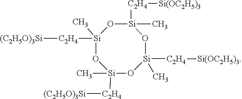
Priority Applications (2)
| Application Number | Priority Date | Filing Date | Title |
|---|---|---|---|
| US15/847,150 US11213976B2 (en) | 2016-12-22 | 2017-12-19 | Imprinting apparatus |
| US17/541,089 US20220088834A1 (en) | 2016-12-22 | 2021-12-02 | Imprinting apparatus |
Applications Claiming Priority (2)
| Application Number | Priority Date | Filing Date | Title |
|---|---|---|---|
| US201662438237P | 2016-12-22 | 2016-12-22 | |
| US15/847,150 US11213976B2 (en) | 2016-12-22 | 2017-12-19 | Imprinting apparatus |
Related Child Applications (1)
| Application Number | Title | Priority Date | Filing Date |
|---|---|---|---|
| US17/541,089 Continuation US20220088834A1 (en) | 2016-12-22 | 2021-12-02 | Imprinting apparatus |
Publications (2)
| Publication Number | Publication Date |
|---|---|
| US20180178416A1 US20180178416A1 (en) | 2018-06-28 |
| US11213976B2 true US11213976B2 (en) | 2022-01-04 |
Family
ID=62625732
Family Applications (2)
| Application Number | Title | Priority Date | Filing Date |
|---|---|---|---|
| US15/847,150 Active 2040-07-24 US11213976B2 (en) | 2016-12-22 | 2017-12-19 | Imprinting apparatus |
| US17/541,089 Pending US20220088834A1 (en) | 2016-12-22 | 2021-12-02 | Imprinting apparatus |
Family Applications After (1)
| Application Number | Title | Priority Date | Filing Date |
|---|---|---|---|
| US17/541,089 Pending US20220088834A1 (en) | 2016-12-22 | 2021-12-02 | Imprinting apparatus |
Country Status (15)
| Country | Link |
|---|---|
| US (2) | US11213976B2 (en) |
| EP (1) | EP3559745B1 (en) |
| JP (1) | JP7084402B2 (en) |
| KR (1) | KR102536039B1 (en) |
| CN (1) | CN110226128A (en) |
| AU (1) | AU2017382163B2 (en) |
| CA (1) | CA3046374A1 (en) |
| IL (1) | IL267443B2 (en) |
| MX (1) | MX2019006512A (en) |
| PH (1) | PH12019501463A1 (en) |
| RU (1) | RU2753172C2 (en) |
| SA (1) | SA519402145B1 (en) |
| TW (1) | TWI823844B (en) |
| WO (1) | WO2018118932A1 (en) |
| ZA (1) | ZA201903897B (en) |
Cited By (1)
| Publication number | Priority date | Publication date | Assignee | Title |
|---|---|---|---|---|
| US20220088834A1 (en) * | 2016-12-22 | 2022-03-24 | Illumina, Inc. | Imprinting apparatus |
Families Citing this family (9)
| Publication number | Priority date | Publication date | Assignee | Title |
|---|---|---|---|---|
| FR3075800B1 (en) * | 2017-12-21 | 2020-10-09 | Arkema France | ANTI-STICK COATS FOR TRANSFER PRINTING PROCESSES |
| KR20210116685A (en) * | 2019-02-11 | 2021-09-27 | 어플라이드 머티어리얼스, 인코포레이티드 | Large-area seamless master and imprint stamp manufacturing method |
| EP3739386A1 (en) | 2019-05-14 | 2020-11-18 | OpTool AB | A stamp material for nanolithography |
| EP3839626B1 (en) * | 2019-12-18 | 2023-10-11 | Nivarox-FAR S.A. | Method for manufacturing a timepiece component |
| AU2021241529A1 (en) * | 2020-03-27 | 2022-10-20 | Illumina, Inc. | Imprinting apparatus |
| EP3929658A1 (en) | 2020-06-23 | 2021-12-29 | Koninklijke Philips N.V. | Imprinting method and patterned layer |
| US11543584B2 (en) * | 2020-07-14 | 2023-01-03 | Meta Platforms Technologies, Llc | Inorganic matrix nanoimprint lithographs and methods of making thereof with reduced carbon |
| JP2024505324A (en) | 2021-01-05 | 2024-02-06 | イルミナ インコーポレイテッド | Composition containing a functional group bonded to a substrate and method for producing the same |
| CN113307223A (en) * | 2021-04-20 | 2021-08-27 | 杭州欧光芯科技有限公司 | Method for modifying local hydrophilicity and hydrophobicity of nanopore |
Citations (52)
| Publication number | Priority date | Publication date | Assignee | Title |
|---|---|---|---|---|
| US4550035A (en) * | 1982-12-10 | 1985-10-29 | Creative Products Resource Associates, Ltd. | Cosmetic applicator useful for skin moisturizing and deodorizing |
| EP0475437A1 (en) | 1990-09-13 | 1992-03-18 | Dow Corning Toray Silicone Company, Limited | Organocyclosiloxane and method for its preparation |
| US5164278A (en) * | 1990-03-01 | 1992-11-17 | International Business Machines Corporation | Speed enhancers for acid sensitized resists |
| US5378790A (en) * | 1992-09-16 | 1995-01-03 | E. I. Du Pont De Nemours & Co. | Single component inorganic/organic network materials and precursors thereof |
| KR0149903B1 (en) * | 1994-01-25 | 1999-03-30 | 제럴드 켄트 화이트 | Waterborne photoresists having polysiloxanes |
| RU2150154C1 (en) | 1998-11-18 | 2000-05-27 | Акционерное общество закрытого типа "Карбид" | Field-effect electron emitter and process of its manufacture ( versions ) |
| WO2000031148A2 (en) | 1998-11-25 | 2000-06-02 | Motorola, Inc. | Polyacrylamide hydrogels and hydrogel arrays made from polyacrylamide reactive prepolymers |
| US6121130A (en) * | 1998-11-16 | 2000-09-19 | Chartered Semiconductor Manufacturing Ltd. | Laser curing of spin-on dielectric thin films |
| WO2001001143A2 (en) | 1999-06-25 | 2001-01-04 | Motorola Inc. | Attachment of biomolecule to a polymeric solid support by cycloaddition of a linker |
| WO2001014493A2 (en) * | 1999-08-20 | 2001-03-01 | Bayer Aktiengesellschaft | Inorganic coating composition, a method for producing same and the use thereof |
| US6309580B1 (en) | 1995-11-15 | 2001-10-30 | Regents Of The University Of Minnesota | Release surfaces, particularly for use in nanoimprint lithography |
| US20020081520A1 (en) * | 2000-12-21 | 2002-06-27 | Ratnam Sooriyakumaran | Substantially transparent aqueous base soluble polymer system for use in 157 nm resist applications |
| WO2003014392A2 (en) | 2001-08-09 | 2003-02-20 | Amersham Biosciences Ab | Use and evaluation of a [2+2] photoaddition in immobilization of oligonucleotides on a three-dimensional hydrogel matrix |
| JP2004066447A (en) * | 2002-06-07 | 2004-03-04 | Canon Inc | Method of manufacturing structure, functional structure, and magnetic recording medium |
| US20040219246A1 (en) * | 2003-04-29 | 2004-11-04 | Jeans Albert H. | Apparatus for embossing a flexible substrate with a pattern carried by an optically transparent compliant media |
| US20050064344A1 (en) * | 2003-09-18 | 2005-03-24 | University Of Texas System Board Of Regents | Imprint lithography templates having alignment marks |
| US20050184397A1 (en) * | 2004-02-19 | 2005-08-25 | International Business Machines Corporation | Structures and methods for intergration of ultralow-k dielectrics with improved reliability |
| JP2005330429A (en) * | 2004-05-21 | 2005-12-02 | Shin Etsu Chem Co Ltd | Curable composition and processed rubber product |
| US20060021967A1 (en) * | 2004-01-27 | 2006-02-02 | Heon Lee | Imprint stamp |
| US20060110940A1 (en) * | 2004-11-24 | 2006-05-25 | Samsung Corning Co., Ltd. | Method of preparing mesoporous thin film having low dielectric constant |
| US20060155074A1 (en) * | 2002-10-04 | 2006-07-13 | Nok Corporation | Sealing material |
| US20060159938A1 (en) * | 2005-01-20 | 2006-07-20 | Samsung Corning Co., Ltd. | Composition for forming low dielectric thin film comprising polymer nanoparticles and method of preparing low dielectric thin film using the same |
| CN101075443A (en) | 2007-06-26 | 2007-11-21 | 西安交通大学 | Method for producing pattern magnetic-recording medium with continuous inverse-impression direct transfer |
| US20080089712A1 (en) | 2006-10-16 | 2008-04-17 | Fuji Xerox Co., Ltd. | Image forming apparatus and process cartridge |
| US20080131692A1 (en) | 2006-12-04 | 2008-06-05 | Liquidia Technologies, Inc. | Methods and materials for fabricating laminate nanomolds and nanoparticles therefrom |
| US20080145525A1 (en) | 2006-12-13 | 2008-06-19 | Xing-Cai Guo | Release layer and resist material for master tool and stamper tool |
| US20090252975A1 (en) * | 2008-04-04 | 2009-10-08 | Samsung Electronics Co., Ltd. | Protective film and encapsulation material comprising the same |
| US20090269942A1 (en) * | 2003-06-30 | 2009-10-29 | Shin Hyeon Jin | Multi-functional cyclic siloxane compound and process for preparing dielectric film by using siloxane-based polymer prepared from the compound |
| JP2010084162A (en) | 2008-09-29 | 2010-04-15 | Asahi Glass Co Ltd | Method for manufacturing replica mold |
| JP2010229324A (en) | 2009-03-27 | 2010-10-14 | Nof Corp | Thermosetting resin composition |
| US7854873B2 (en) | 2005-06-10 | 2010-12-21 | Obducat Ab | Imprint stamp comprising cyclic olefin copolymer |
| US20110039033A1 (en) | 2008-01-31 | 2011-02-17 | Erika Merschrod | Method of depositing a polymer micropattern on a substrate |
| US20110059865A1 (en) | 2004-01-07 | 2011-03-10 | Mark Edward Brennan Smith | Modified Molecular Arrays |
| EP2424949A1 (en) * | 2009-05-01 | 2012-03-07 | Momentive Performance Materials Inc. | Moisture curable silylated polymer compositions containing reactive modifiers |
| WO2012060620A2 (en) | 2010-11-02 | 2012-05-10 | 한국생명공학연구원 | Anti-biofouling ssq/peg network and preparation method thereof |
| US20130059121A1 (en) * | 2005-05-27 | 2013-03-07 | The Governors Of The University Of Alberta | Nanocrystalline silicon in sio2 composite and freestanding silicon nanoparticles |
| US20130122423A1 (en) * | 2010-07-30 | 2013-05-16 | Masatoshi Echigo | Compound, radiation-sensitive composition and resist pattern formation method |
| US20140079923A1 (en) | 2012-06-08 | 2014-03-20 | Wayne N. George | Polymer coatings |
| US20140094004A1 (en) * | 2006-08-15 | 2014-04-03 | Arvind Kamath | Printed Dopant Layers |
| US20140120678A1 (en) * | 2012-10-29 | 2014-05-01 | Matheson Tri-Gas | Methods for Selective and Conformal Epitaxy of Highly Doped Si-containing Materials for Three Dimensional Structures |
| US20140200158A1 (en) | 2011-10-28 | 2014-07-17 | Illumina, Inc. | Microarray fabrication system and method |
| US8877882B1 (en) * | 2013-10-04 | 2014-11-04 | Rochal Industries Llp | Non-self-adherent coating materials |
| US20150005447A1 (en) | 2013-07-01 | 2015-01-01 | Illumina, Inc. | Catalyst-free surface functionalization and polymer grafting |
| US20150136173A1 (en) | 2010-10-29 | 2015-05-21 | Dai Nippon Printing Co., Ltd. | Process and apparatus for cleaning imprinting molds, and process for manufacturing imprinting molds |
| WO2015095291A1 (en) | 2013-12-19 | 2015-06-25 | Illumina, Inc. | Substrates comprising nano-patterning surfaces and methods of preparing thereof |
| US20160023208A1 (en) | 2013-03-13 | 2016-01-28 | Illumina, Inc. | Multilayer fluidic devices and methods for their fabrication |
| US9335628B2 (en) | 2009-09-30 | 2016-05-10 | Fujifilm Corporation | Curable composition for imprints, patterning method and pattern |
| US20160237100A1 (en) * | 2015-02-13 | 2016-08-18 | Air Products And Chemicals, Inc. | Bisaminoalkoxysilane compounds and methods for using same to deposit silicon-containing films |
| CN105903796A (en) * | 2016-04-20 | 2016-08-31 | 深圳市华星光电技术有限公司 | Hook-face displayer back plate forming equipment and method |
| JP2016160285A (en) | 2015-02-26 | 2016-09-05 | 旭化成株式会社 | Photocurable resin composition and method for producing the same |
| US20180333977A1 (en) * | 2015-03-25 | 2018-11-22 | Morpho B.V. | Method of providing an imprinted security feature |
| WO2020000003A1 (en) | 2018-06-27 | 2020-01-02 | Trumpf Maschinen Austria Gmbh & Co. Kg. | Bending tool comprising a spacer element |
Family Cites Families (34)
| Publication number | Priority date | Publication date | Assignee | Title |
|---|---|---|---|---|
| DE3821908A1 (en) * | 1988-06-29 | 1990-01-04 | Ernst Boettler Kg Bomix Chemie | Release agent |
| US5004502A (en) * | 1990-08-23 | 1991-04-02 | Ramzan Chaudhary M | Non-irritating detackifying composition |
| US5330925A (en) * | 1992-06-18 | 1994-07-19 | At&T Bell Laboratories | Method for making a MOS device |
| FR2729406B1 (en) * | 1995-01-16 | 1997-04-18 | Rhone Poulenc Chimie | USE AS ANTI-ADHERENT AND / OR WATER-REPELLANT OF FUNCTIONALIZED POLYORGANOSILOXANES, GRAFTS |
| DE19631227C1 (en) * | 1996-08-02 | 1998-04-23 | Byk Chemie Gmbh | Cyclic siloxane compounds with polyether side chains |
| SG98433A1 (en) * | 1999-12-21 | 2003-09-19 | Ciba Sc Holding Ag | Iodonium salts as latent acid donors |
| JP2004148506A (en) * | 2000-07-21 | 2004-05-27 | Kansai Paint Co Ltd | Coated film and lamination method therefor |
| US6814898B1 (en) * | 2000-10-17 | 2004-11-09 | Seagate Technology Llc | Imprint lithography utilizing room temperature embossing |
| EP1260863A1 (en) * | 2001-05-23 | 2002-11-27 | Scandinavian Micro Biodevices | Micropatterning of plasma polymerized coatings |
| US6743368B2 (en) * | 2002-01-31 | 2004-06-01 | Hewlett-Packard Development Company, L.P. | Nano-size imprinting stamp using spacer technique |
| DE50200638D1 (en) * | 2002-04-16 | 2004-08-19 | Goldschmidt Ag Th | Use of epoxypolysiloxanes modified with oxyalkylene ether groups as additives for radiation-curing coatings |
| DE10217202A1 (en) * | 2002-04-18 | 2003-11-06 | Bayer Ag | Non-stick coatings for reactors |
| JP4024135B2 (en) * | 2002-11-25 | 2007-12-19 | 旭化成ケミカルズ株式会社 | Laser engraving printing plate |
| JP2004325172A (en) * | 2003-04-23 | 2004-11-18 | Asahi Kasei Corp | Microchip using transparent hydrocarbon polymer |
| US20050038180A1 (en) * | 2003-08-13 | 2005-02-17 | Jeans Albert H. | Silicone elastomer material for high-resolution lithography |
| US7365414B2 (en) * | 2003-12-01 | 2008-04-29 | Intel Corporation | Component packaging apparatus, systems, and methods |
| US9040090B2 (en) * | 2003-12-19 | 2015-05-26 | The University Of North Carolina At Chapel Hill | Isolated and fixed micro and nano structures and methods thereof |
| US7563727B2 (en) * | 2004-11-08 | 2009-07-21 | Intel Corporation | Low-k dielectric layer formed from aluminosilicate precursors |
| EP2005248A2 (en) * | 2006-04-11 | 2008-12-24 | Dow Corning Corporation | Low thermal distortion silicone composite molds |
| WO2007127984A2 (en) * | 2006-04-28 | 2007-11-08 | Polyset Company, Inc. | Siloxane epoxy polymers for redistribution layer applications |
| WO2009021249A2 (en) * | 2007-10-29 | 2009-02-12 | Dow Corning Corporation | Polar polydimethylsiloxane molds, methods of making the molds, and methods of using the molds for pattern transfer |
| JP2010280159A (en) * | 2009-06-05 | 2010-12-16 | Osaka Univ | High-durability replica mold for nano-imprint lithography, and method for manufacturing the same |
| CN101923282B (en) * | 2009-06-09 | 2012-01-25 | 清华大学 | Nano-imprint resist and nano-imprint method adopting same |
| US9393737B2 (en) * | 2010-08-06 | 2016-07-19 | Soken Chemical & Engineering Co., Ltd. | Resin mold for nanoimprinting |
| JP2012248641A (en) * | 2011-05-26 | 2012-12-13 | Hyogo Prefecture | Release treatment method for nanoimprint and release film |
| US8586397B2 (en) * | 2011-09-30 | 2013-11-19 | Sunpower Corporation | Method for forming diffusion regions in a silicon substrate |
| US9149958B2 (en) * | 2011-11-14 | 2015-10-06 | Massachusetts Institute Of Technology | Stamp for microcontact printing |
| JP2013138179A (en) * | 2011-11-30 | 2013-07-11 | Central Glass Co Ltd | Photopolymerizable composition and pattern formation method using the same |
| US20130143002A1 (en) * | 2011-12-05 | 2013-06-06 | Seagate Technology Llc | Method and system for optical callibration discs |
| US8874182B2 (en) * | 2013-01-15 | 2014-10-28 | Google Inc. | Encapsulated electronics |
| US9512422B2 (en) * | 2013-02-26 | 2016-12-06 | Illumina, Inc. | Gel patterned surfaces |
| KR20140110543A (en) * | 2013-03-08 | 2014-09-17 | 영창케미칼 주식회사 | A resin composition for replication of nano patterns and the replication method using it |
| US9359512B2 (en) * | 2013-12-23 | 2016-06-07 | Xerox Corporation | Aqueous dispersible siloxane-containing polymer inks useful for printing |
| MX2019006512A (en) * | 2016-12-22 | 2019-10-02 | Illumina Inc | Imprinting apparatus. |
-
2017
- 2017-12-19 MX MX2019006512A patent/MX2019006512A/en unknown
- 2017-12-19 US US15/847,150 patent/US11213976B2/en active Active
- 2017-12-19 EP EP17885170.5A patent/EP3559745B1/en active Active
- 2017-12-19 RU RU2019117478A patent/RU2753172C2/en active
- 2017-12-19 WO PCT/US2017/067333 patent/WO2018118932A1/en active Application Filing
- 2017-12-19 KR KR1020197021371A patent/KR102536039B1/en active IP Right Grant
- 2017-12-19 CN CN201780079812.1A patent/CN110226128A/en active Pending
- 2017-12-19 JP JP2019529959A patent/JP7084402B2/en active Active
- 2017-12-19 IL IL267443A patent/IL267443B2/en unknown
- 2017-12-19 AU AU2017382163A patent/AU2017382163B2/en active Active
- 2017-12-19 CA CA3046374A patent/CA3046374A1/en active Pending
- 2017-12-22 TW TW106145311A patent/TWI823844B/en active
-
2019
- 2019-06-14 ZA ZA2019/03897A patent/ZA201903897B/en unknown
- 2019-06-19 SA SA519402145A patent/SA519402145B1/en unknown
- 2019-06-21 PH PH12019501463A patent/PH12019501463A1/en unknown
-
2021
- 2021-12-02 US US17/541,089 patent/US20220088834A1/en active Pending
Patent Citations (61)
| Publication number | Priority date | Publication date | Assignee | Title |
|---|---|---|---|---|
| US4550035A (en) * | 1982-12-10 | 1985-10-29 | Creative Products Resource Associates, Ltd. | Cosmetic applicator useful for skin moisturizing and deodorizing |
| US5164278A (en) * | 1990-03-01 | 1992-11-17 | International Business Machines Corporation | Speed enhancers for acid sensitized resists |
| EP0475437A1 (en) | 1990-09-13 | 1992-03-18 | Dow Corning Toray Silicone Company, Limited | Organocyclosiloxane and method for its preparation |
| US5378790A (en) * | 1992-09-16 | 1995-01-03 | E. I. Du Pont De Nemours & Co. | Single component inorganic/organic network materials and precursors thereof |
| KR0149903B1 (en) * | 1994-01-25 | 1999-03-30 | 제럴드 켄트 화이트 | Waterborne photoresists having polysiloxanes |
| US6309580B1 (en) | 1995-11-15 | 2001-10-30 | Regents Of The University Of Minnesota | Release surfaces, particularly for use in nanoimprint lithography |
| US6121130A (en) * | 1998-11-16 | 2000-09-19 | Chartered Semiconductor Manufacturing Ltd. | Laser curing of spin-on dielectric thin films |
| RU2150154C1 (en) | 1998-11-18 | 2000-05-27 | Акционерное общество закрытого типа "Карбид" | Field-effect electron emitter and process of its manufacture ( versions ) |
| WO2000031148A2 (en) | 1998-11-25 | 2000-06-02 | Motorola, Inc. | Polyacrylamide hydrogels and hydrogel arrays made from polyacrylamide reactive prepolymers |
| WO2001001143A2 (en) | 1999-06-25 | 2001-01-04 | Motorola Inc. | Attachment of biomolecule to a polymeric solid support by cycloaddition of a linker |
| WO2001014493A2 (en) * | 1999-08-20 | 2001-03-01 | Bayer Aktiengesellschaft | Inorganic coating composition, a method for producing same and the use thereof |
| US20020081520A1 (en) * | 2000-12-21 | 2002-06-27 | Ratnam Sooriyakumaran | Substantially transparent aqueous base soluble polymer system for use in 157 nm resist applications |
| WO2003014392A2 (en) | 2001-08-09 | 2003-02-20 | Amersham Biosciences Ab | Use and evaluation of a [2+2] photoaddition in immobilization of oligonucleotides on a three-dimensional hydrogel matrix |
| JP2004066447A (en) * | 2002-06-07 | 2004-03-04 | Canon Inc | Method of manufacturing structure, functional structure, and magnetic recording medium |
| US20070221448A1 (en) * | 2002-10-04 | 2007-09-27 | Masashi Kudo | Sealing material |
| US20060155074A1 (en) * | 2002-10-04 | 2006-07-13 | Nok Corporation | Sealing material |
| US20090014965A1 (en) * | 2002-10-04 | 2009-01-15 | Nok Corporation | Sealing material |
| US20040219246A1 (en) * | 2003-04-29 | 2004-11-04 | Jeans Albert H. | Apparatus for embossing a flexible substrate with a pattern carried by an optically transparent compliant media |
| US20090269942A1 (en) * | 2003-06-30 | 2009-10-29 | Shin Hyeon Jin | Multi-functional cyclic siloxane compound and process for preparing dielectric film by using siloxane-based polymer prepared from the compound |
| US20050064344A1 (en) * | 2003-09-18 | 2005-03-24 | University Of Texas System Board Of Regents | Imprint lithography templates having alignment marks |
| US20110059865A1 (en) | 2004-01-07 | 2011-03-10 | Mark Edward Brennan Smith | Modified Molecular Arrays |
| US20060021967A1 (en) * | 2004-01-27 | 2006-02-02 | Heon Lee | Imprint stamp |
| US20050184397A1 (en) * | 2004-02-19 | 2005-08-25 | International Business Machines Corporation | Structures and methods for intergration of ultralow-k dielectrics with improved reliability |
| JP2005330429A (en) * | 2004-05-21 | 2005-12-02 | Shin Etsu Chem Co Ltd | Curable composition and processed rubber product |
| US20060110940A1 (en) * | 2004-11-24 | 2006-05-25 | Samsung Corning Co., Ltd. | Method of preparing mesoporous thin film having low dielectric constant |
| US20060159938A1 (en) * | 2005-01-20 | 2006-07-20 | Samsung Corning Co., Ltd. | Composition for forming low dielectric thin film comprising polymer nanoparticles and method of preparing low dielectric thin film using the same |
| US20130059121A1 (en) * | 2005-05-27 | 2013-03-07 | The Governors Of The University Of Alberta | Nanocrystalline silicon in sio2 composite and freestanding silicon nanoparticles |
| US7854873B2 (en) | 2005-06-10 | 2010-12-21 | Obducat Ab | Imprint stamp comprising cyclic olefin copolymer |
| US20140094004A1 (en) * | 2006-08-15 | 2014-04-03 | Arvind Kamath | Printed Dopant Layers |
| US20080089712A1 (en) | 2006-10-16 | 2008-04-17 | Fuji Xerox Co., Ltd. | Image forming apparatus and process cartridge |
| CN101165605A (en) | 2006-10-16 | 2008-04-23 | 富士施乐株式会社 | Image forming apparatus and process cartridge |
| US20080131692A1 (en) | 2006-12-04 | 2008-06-05 | Liquidia Technologies, Inc. | Methods and materials for fabricating laminate nanomolds and nanoparticles therefrom |
| US7604836B2 (en) | 2006-12-13 | 2009-10-20 | Hitachi Global Storage Technologies Netherlands B.V. | Release layer and resist material for master tool and stamper tool |
| US20080145525A1 (en) | 2006-12-13 | 2008-06-19 | Xing-Cai Guo | Release layer and resist material for master tool and stamper tool |
| CN101075443A (en) | 2007-06-26 | 2007-11-21 | 西安交通大学 | Method for producing pattern magnetic-recording medium with continuous inverse-impression direct transfer |
| US20110039033A1 (en) | 2008-01-31 | 2011-02-17 | Erika Merschrod | Method of depositing a polymer micropattern on a substrate |
| US20090252975A1 (en) * | 2008-04-04 | 2009-10-08 | Samsung Electronics Co., Ltd. | Protective film and encapsulation material comprising the same |
| JP2010084162A (en) | 2008-09-29 | 2010-04-15 | Asahi Glass Co Ltd | Method for manufacturing replica mold |
| JP2010229324A (en) | 2009-03-27 | 2010-10-14 | Nof Corp | Thermosetting resin composition |
| EP2424949A1 (en) * | 2009-05-01 | 2012-03-07 | Momentive Performance Materials Inc. | Moisture curable silylated polymer compositions containing reactive modifiers |
| US9335628B2 (en) | 2009-09-30 | 2016-05-10 | Fujifilm Corporation | Curable composition for imprints, patterning method and pattern |
| US20130122423A1 (en) * | 2010-07-30 | 2013-05-16 | Masatoshi Echigo | Compound, radiation-sensitive composition and resist pattern formation method |
| US20150136173A1 (en) | 2010-10-29 | 2015-05-21 | Dai Nippon Printing Co., Ltd. | Process and apparatus for cleaning imprinting molds, and process for manufacturing imprinting molds |
| WO2012060620A2 (en) | 2010-11-02 | 2012-05-10 | 한국생명공학연구원 | Anti-biofouling ssq/peg network and preparation method thereof |
| US20140200158A1 (en) | 2011-10-28 | 2014-07-17 | Illumina, Inc. | Microarray fabrication system and method |
| US20140079923A1 (en) | 2012-06-08 | 2014-03-20 | Wayne N. George | Polymer coatings |
| US9012022B2 (en) | 2012-06-08 | 2015-04-21 | Illumina, Inc. | Polymer coatings |
| US20140120678A1 (en) * | 2012-10-29 | 2014-05-01 | Matheson Tri-Gas | Methods for Selective and Conformal Epitaxy of Highly Doped Si-containing Materials for Three Dimensional Structures |
| US20160023208A1 (en) | 2013-03-13 | 2016-01-28 | Illumina, Inc. | Multilayer fluidic devices and methods for their fabrication |
| WO2015002813A1 (en) | 2013-07-01 | 2015-01-08 | Illumina, Inc. | Catalyst-free surface functionalization and polymer grafting |
| US20150005447A1 (en) | 2013-07-01 | 2015-01-01 | Illumina, Inc. | Catalyst-free surface functionalization and polymer grafting |
| CN105431554A (en) | 2013-07-01 | 2016-03-23 | Illumina公司 | Catalyst-free surface functionalization and polymer grafting |
| US8877882B1 (en) * | 2013-10-04 | 2014-11-04 | Rochal Industries Llp | Non-self-adherent coating materials |
| WO2015095291A1 (en) | 2013-12-19 | 2015-06-25 | Illumina, Inc. | Substrates comprising nano-patterning surfaces and methods of preparing thereof |
| US20160246170A1 (en) * | 2013-12-19 | 2016-08-25 | Illumina, Inc. | Substrates comprising nano-patterning surfaces and methods of preparing thereof |
| US10682829B2 (en) * | 2013-12-19 | 2020-06-16 | Illumina, Inc. | Substrates comprising nano-patterning surfaces and methods of preparing thereof |
| US20160237100A1 (en) * | 2015-02-13 | 2016-08-18 | Air Products And Chemicals, Inc. | Bisaminoalkoxysilane compounds and methods for using same to deposit silicon-containing films |
| JP2016160285A (en) | 2015-02-26 | 2016-09-05 | 旭化成株式会社 | Photocurable resin composition and method for producing the same |
| US20180333977A1 (en) * | 2015-03-25 | 2018-11-22 | Morpho B.V. | Method of providing an imprinted security feature |
| CN105903796A (en) * | 2016-04-20 | 2016-08-31 | 深圳市华星光电技术有限公司 | Hook-face displayer back plate forming equipment and method |
| WO2020000003A1 (en) | 2018-06-27 | 2020-01-02 | Trumpf Maschinen Austria Gmbh & Co. Kg. | Bending tool comprising a spacer element |
Non-Patent Citations (13)
| Title |
|---|
| CN 105903796 WIPO Patentscope Translation of Specification and Claims (Year: 2021). * |
| CN104817702 WIPO Patenscope Translation of Specification and Claims (Year: 2021). * |
| EP2424949 Wipo Patentscope Translation of Specification and Claims (Year: 2021). * |
| International Search Report and Written Opinion for International Application No. PCT/US2017/067333 dated Apr. 27, 2018, 16 pages. |
| JP 2005/330429 WIPO Patentscope Translation of Specification and Claims (Year: 2021). * |
| JP 2016/160285 WIPO Patentscope Translation of Specification and Claims (Year: 2021). * |
| KR 0149903 WIPO Patentscope Translation (Year: 2021). * |
| Ro, H.W., et al., "Cubic Silsesquioxanes as a Green, High-Performance Mold Material for Nanoimprint Lithography", Adv. Mater. 2011, pp. 414-420. |
| SciFinder Molecular Search Results (Year: 2021). * |
| STIC Molecular Search Results (Year: 2021). * |
| STN Next Molecular Search Results (Year: 2021). * |
| WO0114493A2 WIPO Patentscope Translation of Specification and Claims (Year: 2021). * |
| WO2015/095291 Patentscope Translation of Specification and Claims (Year: 2021). * |
Cited By (1)
| Publication number | Priority date | Publication date | Assignee | Title |
|---|---|---|---|---|
| US20220088834A1 (en) * | 2016-12-22 | 2022-03-24 | Illumina, Inc. | Imprinting apparatus |
Also Published As
| Publication number | Publication date |
|---|---|
| RU2019117478A (en) | 2021-01-25 |
| US20220088834A1 (en) | 2022-03-24 |
| BR112019013075A2 (en) | 2020-02-04 |
| TW201841716A (en) | 2018-12-01 |
| CA3046374A1 (en) | 2018-06-28 |
| IL267443B1 (en) | 2023-06-01 |
| EP3559745A1 (en) | 2019-10-30 |
| EP3559745A4 (en) | 2020-11-11 |
| JP7084402B2 (en) | 2022-06-14 |
| JP2020501937A (en) | 2020-01-23 |
| MX2019006512A (en) | 2019-10-02 |
| US20180178416A1 (en) | 2018-06-28 |
| CN110226128A (en) | 2019-09-10 |
| IL267443B2 (en) | 2023-10-01 |
| IL267443A (en) | 2019-08-29 |
| AU2017382163B2 (en) | 2022-06-09 |
| WO2018118932A1 (en) | 2018-06-28 |
| AU2017382163A1 (en) | 2019-06-20 |
| TWI823844B (en) | 2023-12-01 |
| KR102536039B1 (en) | 2023-05-23 |
| KR20190099279A (en) | 2019-08-26 |
| SA519402145B1 (en) | 2022-11-08 |
| ZA201903897B (en) | 2022-10-26 |
| EP3559745B1 (en) | 2024-02-14 |
| RU2753172C2 (en) | 2021-08-12 |
| RU2019117478A3 (en) | 2021-01-27 |
| PH12019501463A1 (en) | 2020-03-09 |
Similar Documents
| Publication | Publication Date | Title |
|---|---|---|
| US20220088834A1 (en) | Imprinting apparatus | |
| US11680292B2 (en) | Flow cells | |
| US11932900B2 (en) | Arrays including a resin film and a patterned polymer layer | |
| CN114174802A (en) | Flow cell | |
| BR112019013075B1 (en) | PRINTING DEVICE | |
| US11886110B2 (en) | Imprinting apparatus | |
| TW202335738A (en) | Flow cells and methods for making the same |
Legal Events
| Date | Code | Title | Description |
|---|---|---|---|
| FEPP | Fee payment procedure |
Free format text: ENTITY STATUS SET TO UNDISCOUNTED (ORIGINAL EVENT CODE: BIG.); ENTITY STATUS OF PATENT OWNER: LARGE ENTITY |
|
| AS | Assignment |
Owner name: ILLUMINA, INC., CALIFORNIA Free format text: ASSIGNMENT OF ASSIGNORS INTEREST;ASSIGNORS:MERKEL, TIMOTHY J.;ZAK, AUDREY ROSE;SIGNING DATES FROM 20180424 TO 20180531;REEL/FRAME:046318/0197 Owner name: ILLUMINA CAMBRIDGE LIMITED, GREAT BRITAIN Free format text: ASSIGNMENT OF ASSIGNORS INTEREST;ASSIGNORS:RICHEZ, ALEXANDRE;BROWN, ANDREW A.;MORRISON, JULIA;AND OTHERS;REEL/FRAME:046015/0652 Effective date: 20180425 |
|
| STPP | Information on status: patent application and granting procedure in general |
Free format text: DOCKETED NEW CASE - READY FOR EXAMINATION |
|
| STPP | Information on status: patent application and granting procedure in general |
Free format text: RESPONSE TO NON-FINAL OFFICE ACTION ENTERED AND FORWARDED TO EXAMINER |
|
| STPP | Information on status: patent application and granting procedure in general |
Free format text: NON FINAL ACTION MAILED |
|
| STPP | Information on status: patent application and granting procedure in general |
Free format text: RESPONSE TO NON-FINAL OFFICE ACTION ENTERED AND FORWARDED TO EXAMINER |
|
| STPP | Information on status: patent application and granting procedure in general |
Free format text: NOTICE OF ALLOWANCE MAILED -- APPLICATION RECEIVED IN OFFICE OF PUBLICATIONS |
|
| STPP | Information on status: patent application and granting procedure in general |
Free format text: PUBLICATIONS -- ISSUE FEE PAYMENT RECEIVED |
|
| STPP | Information on status: patent application and granting procedure in general |
Free format text: PUBLICATIONS -- ISSUE FEE PAYMENT VERIFIED |
|
| STCF | Information on status: patent grant |
Free format text: PATENTED CASE |