US11088571B2 - Electronic apparatus and display apparatus, and method for operating apparatuses - Google Patents
Electronic apparatus and display apparatus, and method for operating apparatuses Download PDFInfo
- Publication number
- US11088571B2 US11088571B2 US16/318,492 US201716318492A US11088571B2 US 11088571 B2 US11088571 B2 US 11088571B2 US 201716318492 A US201716318492 A US 201716318492A US 11088571 B2 US11088571 B2 US 11088571B2
- Authority
- US
- United States
- Prior art keywords
- distance
- wireless power
- display apparatus
- voltage
- inverter
- Prior art date
- Legal status (The legal status is an assumption and is not a legal conclusion. Google has not performed a legal analysis and makes no representation as to the accuracy of the status listed.)
- Active
Links
Images


Classifications
-
- H—ELECTRICITY
- H02—GENERATION; CONVERSION OR DISTRIBUTION OF ELECTRIC POWER
- H02J—CIRCUIT ARRANGEMENTS OR SYSTEMS FOR SUPPLYING OR DISTRIBUTING ELECTRIC POWER; SYSTEMS FOR STORING ELECTRIC ENERGY
- H02J50/00—Circuit arrangements or systems for wireless supply or distribution of electric power
- H02J50/10—Circuit arrangements or systems for wireless supply or distribution of electric power using inductive coupling
- H02J50/12—Circuit arrangements or systems for wireless supply or distribution of electric power using inductive coupling of the resonant type
-
- G—PHYSICS
- G09—EDUCATION; CRYPTOGRAPHY; DISPLAY; ADVERTISING; SEALS
- G09G—ARRANGEMENTS OR CIRCUITS FOR CONTROL OF INDICATING DEVICES USING STATIC MEANS TO PRESENT VARIABLE INFORMATION
- G09G3/00—Control arrangements or circuits, of interest only in connection with visual indicators other than cathode-ray tubes
- G09G3/20—Control arrangements or circuits, of interest only in connection with visual indicators other than cathode-ray tubes for presentation of an assembly of a number of characters, e.g. a page, by composing the assembly by combination of individual elements arranged in a matrix no fixed position being assigned to or needed to be assigned to the individual characters or partial characters
- G09G3/2092—Details of a display terminals using a flat panel, the details relating to the control arrangement of the display terminal and to the interfaces thereto
- G09G3/2096—Details of the interface to the display terminal specific for a flat panel
-
- H—ELECTRICITY
- H02—GENERATION; CONVERSION OR DISTRIBUTION OF ELECTRIC POWER
- H02M—APPARATUS FOR CONVERSION BETWEEN AC AND AC, BETWEEN AC AND DC, OR BETWEEN DC AND DC, AND FOR USE WITH MAINS OR SIMILAR POWER SUPPLY SYSTEMS; CONVERSION OF DC OR AC INPUT POWER INTO SURGE OUTPUT POWER; CONTROL OR REGULATION THEREOF
- H02M1/00—Details of apparatus for conversion
- H02M1/0048—Circuits or arrangements for reducing losses
- H02M1/0054—Transistor switching losses
- H02M1/0058—Transistor switching losses by employing soft switching techniques, i.e. commutation of transistors when applied voltage is zero or when current flow is zero
-
- H—ELECTRICITY
- H02—GENERATION; CONVERSION OR DISTRIBUTION OF ELECTRIC POWER
- H02M—APPARATUS FOR CONVERSION BETWEEN AC AND AC, BETWEEN AC AND DC, OR BETWEEN DC AND DC, AND FOR USE WITH MAINS OR SIMILAR POWER SUPPLY SYSTEMS; CONVERSION OF DC OR AC INPUT POWER INTO SURGE OUTPUT POWER; CONTROL OR REGULATION THEREOF
- H02M1/00—Details of apparatus for conversion
- H02M1/08—Circuits specially adapted for the generation of control voltages for semiconductor devices incorporated in static converters
- H02M1/083—Circuits specially adapted for the generation of control voltages for semiconductor devices incorporated in static converters for the ignition at the zero crossing of the voltage or the current
-
- H—ELECTRICITY
- H02—GENERATION; CONVERSION OR DISTRIBUTION OF ELECTRIC POWER
- H02M—APPARATUS FOR CONVERSION BETWEEN AC AND AC, BETWEEN AC AND DC, OR BETWEEN DC AND DC, AND FOR USE WITH MAINS OR SIMILAR POWER SUPPLY SYSTEMS; CONVERSION OF DC OR AC INPUT POWER INTO SURGE OUTPUT POWER; CONTROL OR REGULATION THEREOF
- H02M3/00—Conversion of dc power input into dc power output
- H02M3/22—Conversion of dc power input into dc power output with intermediate conversion into ac
- H02M3/24—Conversion of dc power input into dc power output with intermediate conversion into ac by static converters
- H02M3/28—Conversion of dc power input into dc power output with intermediate conversion into ac by static converters using discharge tubes with control electrode or semiconductor devices with control electrode to produce the intermediate ac
-
- H—ELECTRICITY
- H02—GENERATION; CONVERSION OR DISTRIBUTION OF ELECTRIC POWER
- H02M—APPARATUS FOR CONVERSION BETWEEN AC AND AC, BETWEEN AC AND DC, OR BETWEEN DC AND DC, AND FOR USE WITH MAINS OR SIMILAR POWER SUPPLY SYSTEMS; CONVERSION OF DC OR AC INPUT POWER INTO SURGE OUTPUT POWER; CONTROL OR REGULATION THEREOF
- H02M7/00—Conversion of ac power input into dc power output; Conversion of dc power input into ac power output
- H02M7/42—Conversion of dc power input into ac power output without possibility of reversal
- H02M7/44—Conversion of dc power input into ac power output without possibility of reversal by static converters
- H02M7/48—Conversion of dc power input into ac power output without possibility of reversal by static converters using discharge tubes with control electrode or semiconductor devices with control electrode
- H02M7/53—Conversion of dc power input into ac power output without possibility of reversal by static converters using discharge tubes with control electrode or semiconductor devices with control electrode using devices of a triode or transistor type requiring continuous application of a control signal
- H02M7/537—Conversion of dc power input into ac power output without possibility of reversal by static converters using discharge tubes with control electrode or semiconductor devices with control electrode using devices of a triode or transistor type requiring continuous application of a control signal using semiconductor devices only, e.g. single switched pulse inverters
- H02M7/5387—Conversion of dc power input into ac power output without possibility of reversal by static converters using discharge tubes with control electrode or semiconductor devices with control electrode using devices of a triode or transistor type requiring continuous application of a control signal using semiconductor devices only, e.g. single switched pulse inverters in a bridge configuration
- H02M7/53871—Conversion of dc power input into ac power output without possibility of reversal by static converters using discharge tubes with control electrode or semiconductor devices with control electrode using devices of a triode or transistor type requiring continuous application of a control signal using semiconductor devices only, e.g. single switched pulse inverters in a bridge configuration with automatic control of output voltage or current
-
- G—PHYSICS
- G09—EDUCATION; CRYPTOGRAPHY; DISPLAY; ADVERTISING; SEALS
- G09G—ARRANGEMENTS OR CIRCUITS FOR CONTROL OF INDICATING DEVICES USING STATIC MEANS TO PRESENT VARIABLE INFORMATION
- G09G2310/00—Command of the display device
- G09G2310/08—Details of timing specific for flat panels, other than clock recovery
-
- G—PHYSICS
- G09—EDUCATION; CRYPTOGRAPHY; DISPLAY; ADVERTISING; SEALS
- G09G—ARRANGEMENTS OR CIRCUITS FOR CONTROL OF INDICATING DEVICES USING STATIC MEANS TO PRESENT VARIABLE INFORMATION
- G09G2330/00—Aspects of power supply; Aspects of display protection and defect management
- G09G2330/02—Details of power systems and of start or stop of display operation
- G09G2330/028—Generation of voltages supplied to electrode drivers in a matrix display other than LCD
-
- G—PHYSICS
- G09—EDUCATION; CRYPTOGRAPHY; DISPLAY; ADVERTISING; SEALS
- G09G—ARRANGEMENTS OR CIRCUITS FOR CONTROL OF INDICATING DEVICES USING STATIC MEANS TO PRESENT VARIABLE INFORMATION
- G09G3/00—Control arrangements or circuits, of interest only in connection with visual indicators other than cathode-ray tubes
- G09G3/20—Control arrangements or circuits, of interest only in connection with visual indicators other than cathode-ray tubes for presentation of an assembly of a number of characters, e.g. a page, by composing the assembly by combination of individual elements arranged in a matrix no fixed position being assigned to or needed to be assigned to the individual characters or partial characters
- G09G3/22—Control arrangements or circuits, of interest only in connection with visual indicators other than cathode-ray tubes for presentation of an assembly of a number of characters, e.g. a page, by composing the assembly by combination of individual elements arranged in a matrix no fixed position being assigned to or needed to be assigned to the individual characters or partial characters using controlled light sources
- G09G3/30—Control arrangements or circuits, of interest only in connection with visual indicators other than cathode-ray tubes for presentation of an assembly of a number of characters, e.g. a page, by composing the assembly by combination of individual elements arranged in a matrix no fixed position being assigned to or needed to be assigned to the individual characters or partial characters using controlled light sources using electroluminescent panels
- G09G3/32—Control arrangements or circuits, of interest only in connection with visual indicators other than cathode-ray tubes for presentation of an assembly of a number of characters, e.g. a page, by composing the assembly by combination of individual elements arranged in a matrix no fixed position being assigned to or needed to be assigned to the individual characters or partial characters using controlled light sources using electroluminescent panels semiconductive, e.g. using light-emitting diodes [LED]
- G09G3/3208—Control arrangements or circuits, of interest only in connection with visual indicators other than cathode-ray tubes for presentation of an assembly of a number of characters, e.g. a page, by composing the assembly by combination of individual elements arranged in a matrix no fixed position being assigned to or needed to be assigned to the individual characters or partial characters using controlled light sources using electroluminescent panels semiconductive, e.g. using light-emitting diodes [LED] organic, e.g. using organic light-emitting diodes [OLED]
- G09G3/3225—Control arrangements or circuits, of interest only in connection with visual indicators other than cathode-ray tubes for presentation of an assembly of a number of characters, e.g. a page, by composing the assembly by combination of individual elements arranged in a matrix no fixed position being assigned to or needed to be assigned to the individual characters or partial characters using controlled light sources using electroluminescent panels semiconductive, e.g. using light-emitting diodes [LED] organic, e.g. using organic light-emitting diodes [OLED] using an active matrix
- G09G3/3233—Control arrangements or circuits, of interest only in connection with visual indicators other than cathode-ray tubes for presentation of an assembly of a number of characters, e.g. a page, by composing the assembly by combination of individual elements arranged in a matrix no fixed position being assigned to or needed to be assigned to the individual characters or partial characters using controlled light sources using electroluminescent panels semiconductive, e.g. using light-emitting diodes [LED] organic, e.g. using organic light-emitting diodes [OLED] using an active matrix with pixel circuitry controlling the current through the light-emitting element
-
- G—PHYSICS
- G09—EDUCATION; CRYPTOGRAPHY; DISPLAY; ADVERTISING; SEALS
- G09G—ARRANGEMENTS OR CIRCUITS FOR CONTROL OF INDICATING DEVICES USING STATIC MEANS TO PRESENT VARIABLE INFORMATION
- G09G3/00—Control arrangements or circuits, of interest only in connection with visual indicators other than cathode-ray tubes
- G09G3/20—Control arrangements or circuits, of interest only in connection with visual indicators other than cathode-ray tubes for presentation of an assembly of a number of characters, e.g. a page, by composing the assembly by combination of individual elements arranged in a matrix no fixed position being assigned to or needed to be assigned to the individual characters or partial characters
- G09G3/22—Control arrangements or circuits, of interest only in connection with visual indicators other than cathode-ray tubes for presentation of an assembly of a number of characters, e.g. a page, by composing the assembly by combination of individual elements arranged in a matrix no fixed position being assigned to or needed to be assigned to the individual characters or partial characters using controlled light sources
- G09G3/30—Control arrangements or circuits, of interest only in connection with visual indicators other than cathode-ray tubes for presentation of an assembly of a number of characters, e.g. a page, by composing the assembly by combination of individual elements arranged in a matrix no fixed position being assigned to or needed to be assigned to the individual characters or partial characters using controlled light sources using electroluminescent panels
- G09G3/32—Control arrangements or circuits, of interest only in connection with visual indicators other than cathode-ray tubes for presentation of an assembly of a number of characters, e.g. a page, by composing the assembly by combination of individual elements arranged in a matrix no fixed position being assigned to or needed to be assigned to the individual characters or partial characters using controlled light sources using electroluminescent panels semiconductive, e.g. using light-emitting diodes [LED]
- G09G3/3208—Control arrangements or circuits, of interest only in connection with visual indicators other than cathode-ray tubes for presentation of an assembly of a number of characters, e.g. a page, by composing the assembly by combination of individual elements arranged in a matrix no fixed position being assigned to or needed to be assigned to the individual characters or partial characters using controlled light sources using electroluminescent panels semiconductive, e.g. using light-emitting diodes [LED] organic, e.g. using organic light-emitting diodes [OLED]
- G09G3/3266—Details of drivers for scan electrodes
-
- G—PHYSICS
- G09—EDUCATION; CRYPTOGRAPHY; DISPLAY; ADVERTISING; SEALS
- G09G—ARRANGEMENTS OR CIRCUITS FOR CONTROL OF INDICATING DEVICES USING STATIC MEANS TO PRESENT VARIABLE INFORMATION
- G09G3/00—Control arrangements or circuits, of interest only in connection with visual indicators other than cathode-ray tubes
- G09G3/20—Control arrangements or circuits, of interest only in connection with visual indicators other than cathode-ray tubes for presentation of an assembly of a number of characters, e.g. a page, by composing the assembly by combination of individual elements arranged in a matrix no fixed position being assigned to or needed to be assigned to the individual characters or partial characters
- G09G3/22—Control arrangements or circuits, of interest only in connection with visual indicators other than cathode-ray tubes for presentation of an assembly of a number of characters, e.g. a page, by composing the assembly by combination of individual elements arranged in a matrix no fixed position being assigned to or needed to be assigned to the individual characters or partial characters using controlled light sources
- G09G3/30—Control arrangements or circuits, of interest only in connection with visual indicators other than cathode-ray tubes for presentation of an assembly of a number of characters, e.g. a page, by composing the assembly by combination of individual elements arranged in a matrix no fixed position being assigned to or needed to be assigned to the individual characters or partial characters using controlled light sources using electroluminescent panels
- G09G3/32—Control arrangements or circuits, of interest only in connection with visual indicators other than cathode-ray tubes for presentation of an assembly of a number of characters, e.g. a page, by composing the assembly by combination of individual elements arranged in a matrix no fixed position being assigned to or needed to be assigned to the individual characters or partial characters using controlled light sources using electroluminescent panels semiconductive, e.g. using light-emitting diodes [LED]
- G09G3/3208—Control arrangements or circuits, of interest only in connection with visual indicators other than cathode-ray tubes for presentation of an assembly of a number of characters, e.g. a page, by composing the assembly by combination of individual elements arranged in a matrix no fixed position being assigned to or needed to be assigned to the individual characters or partial characters using controlled light sources using electroluminescent panels semiconductive, e.g. using light-emitting diodes [LED] organic, e.g. using organic light-emitting diodes [OLED]
- G09G3/3275—Details of drivers for data electrodes
-
- H—ELECTRICITY
- H02—GENERATION; CONVERSION OR DISTRIBUTION OF ELECTRIC POWER
- H02M—APPARATUS FOR CONVERSION BETWEEN AC AND AC, BETWEEN AC AND DC, OR BETWEEN DC AND DC, AND FOR USE WITH MAINS OR SIMILAR POWER SUPPLY SYSTEMS; CONVERSION OF DC OR AC INPUT POWER INTO SURGE OUTPUT POWER; CONTROL OR REGULATION THEREOF
- H02M1/00—Details of apparatus for conversion
- H02M1/42—Circuits or arrangements for compensating for or adjusting power factor in converters or inverters
- H02M1/4208—Arrangements for improving power factor of AC input
-
- H—ELECTRICITY
- H02—GENERATION; CONVERSION OR DISTRIBUTION OF ELECTRIC POWER
- H02M—APPARATUS FOR CONVERSION BETWEEN AC AND AC, BETWEEN AC AND DC, OR BETWEEN DC AND DC, AND FOR USE WITH MAINS OR SIMILAR POWER SUPPLY SYSTEMS; CONVERSION OF DC OR AC INPUT POWER INTO SURGE OUTPUT POWER; CONTROL OR REGULATION THEREOF
- H02M1/00—Details of apparatus for conversion
- H02M1/44—Circuits or arrangements for compensating for electromagnetic interference in converters or inverters
-
- Y—GENERAL TAGGING OF NEW TECHNOLOGICAL DEVELOPMENTS; GENERAL TAGGING OF CROSS-SECTIONAL TECHNOLOGIES SPANNING OVER SEVERAL SECTIONS OF THE IPC; TECHNICAL SUBJECTS COVERED BY FORMER USPC CROSS-REFERENCE ART COLLECTIONS [XRACs] AND DIGESTS
- Y02—TECHNOLOGIES OR APPLICATIONS FOR MITIGATION OR ADAPTATION AGAINST CLIMATE CHANGE
- Y02B—CLIMATE CHANGE MITIGATION TECHNOLOGIES RELATED TO BUILDINGS, e.g. HOUSING, HOUSE APPLIANCES OR RELATED END-USER APPLICATIONS
- Y02B70/00—Technologies for an efficient end-user side electric power management and consumption
- Y02B70/10—Technologies improving the efficiency by using switched-mode power supplies [SMPS], i.e. efficient power electronics conversion e.g. power factor correction or reduction of losses in power supplies or efficient standby modes
Definitions
- Devices and methods consistent with what is disclosed herein relate to an electronic apparatus, a display apparatus, an operational method thereof, and more particularly, to a display apparatus such as a DTV for receiving power regardless of a distance from a peripheral apparatus and maintaining target power constantly, a display apparatus, an operational method thereof.
- Wireless power transfer is a technique for transmitting power wirelessly.
- the wireless power transfer is referred to as Wi-power similarly to a Wi-Fi technique which enables free Internet access only with a wireless adaptor anytime and anywhere.
- the wireless power transfer is categorized by an Inductive Power Transfer System (IPTS) method used for wireless charge, a Coupled Magnetic Resonance System (CMRS) method to be used for an electric vehicle, a high-speed train, etc., and a long distance microwave method using space solar power, which is an ongoing project.
- IPTS Inductive Power Transfer System
- CMRS Coupled Magnetic Resonance System
- a long distance microwave method using space solar power which is an ongoing project.
- Such technique may be applied to a TV without change, but considering the characteristic of a TV, a wall-mounted TV can be installed in various manners and in various spaces depending on a user. Therefore, it becomes difficult to transmit stable power.
- One technical task of the present disclosure is to provide an electronic apparatus such as a DTV for receiving power regardless of a distance from a peripheral apparatus and maintaining target power constantly, a display apparatus, an operational method thereof.
- a display apparatus including a resonance circuit unit configured to receive power by using an inductive electromotive force through magnetic field generated by an external apparatus including a high-frequency operating inverter and a transmission coil (or a first coil unit), a rectifier configured to rectify an output voltage of the resonance circuit unit, and a converter configured to vary a frequency and a duty based on a target voltage and duty data determined in accordance with a distance from an external apparatus and output the rectified output voltage of the rectifier as the target voltage.
- the converter may change an effective resistance value of a load resistance connected to the converter by varying the frequency and the duty, and adjust the rectified output voltage to the target voltage to output.
- the converter may be a topology transformable DC-DC converter in a half-bridge type of in a full-bridge type to output a constant target voltage based on a variation of a receiving voltage depending on a distance being large (e.g. 100V to 400V). Based on the receiving voltage being large (e.g. 250V to 400V), the converter may operate in a half-bridge method, and based on the receiving voltage being small (e.g. 100V to 250V), operate in a full-bridge method.
- a receiving voltage e.g. 250V to 400V
- the display apparatus may further include a processor configured to, based on the distance being within a predetermined distance and an internal resistance of the converter exceeding a threshold value, operate the converter at a predetermined frequency and a predetermined duty, and request the external apparatus to change an operating frequency and a duty of an inverter.
- a processor configured to, based on the distance being within a predetermined distance and an internal resistance of the converter exceeding a threshold value, operate the converter at a predetermined frequency and a predetermined duty, and request the external apparatus to change an operating frequency and a duty of an inverter.
- an electronic apparatus including an interface unit configured to process at least one of a video signal and(or) an audio signal while being operable in association with a display apparatus, an inverter configured to operate at an operating frequency determined in accordance with a distance from the display apparatus and change a DC voltage input from an outside into an AC voltage, and a second coil unit configured to receive magnetic field generated by the AC voltage from the display apparatus and generate an inductive electromotive force.
- the electronic apparatus may include a peripheral apparatus disposed near the display apparatus.
- the electronic apparatus may include a processor configured to measure the distance during initial driving of the electronic apparatus, and operate the inverter at an operating frequency corresponding to the measured distance.
- the processor may be configured to measure the distance using a down-scanning method that reduces an operating frequency or using an up-scanning method that increases an operating frequency.
- the processor may identify a resonance point based on a maximum value among values sensed by using the up-scanning method, determine a distance based on the resonance point, and determine a predetermined (optimal) operating frequency/duty of an inverter.
- the electronic apparatus may further include a ZVS element provided between an output end of the inverter and a resonance coil, and configured to perform a zero voltage switching (ZVS) operation of a plurality of switching elements included in the inverter based on the distance exceeding a threshold value.
- ZVS zero voltage switching
- the electronic apparatus may perform down-scanning or up-scanning while a parallel capacitor is connected to a series resonance circuit of a power receiving unit to prevent a no-load condition of the power receiving unit included in the display apparatus.
- the electronic apparatus may scan an input voltage of the inverter by applying a voltage lower than a voltage necessary for a maximum load operation reference of a power receiving unit included in the display apparatus, or by setting a duty of the inverter to a low level and lowering an effective input voltage of the inverter.
- the electronic apparatus may perform an initial scanning operation in a state where a switch between a receiver-converter included in the display apparatus and load is turned off, and perform normal wireless power transmission in a state where the switch is turned on.
- a method for driving a display apparatus including generating a voltage by using an inductive electromotive force generated by an external apparatus, rectifying an output voltage of a resonance circuit unit, and varying a frequency and a duty of a receiver-converter based on a target voltage and duty data of an inverter determined in accordance with a distance from the external apparatus and outputting the rectified output voltage of a rectifier as the target voltage.
- the outputting may comprise changing an effective resistance value of a load resistance connected to the converter through duty/frequency variance of the converter and generating the rectified output voltage as the target voltage to output.
- the converter may perform DC-DC converting.
- the method may further include operating the inverter in a half-bridge method based on the distance being out of a predetermined distance, and operating the inverted in a full-bridge method based on the distance within the predetermined distance.
- the method may further include operating the converter at a predetermined duty based on the distance being within a predetermined distance and an internal resistance of the converter exceeding a threshold value, and requesting the external apparatus to change an operating frequency/duty of an inverter.
- a method for driving an electronic apparatus including processing at least one of a video signal or an audio signal while being operable in association with a display apparatus, operating at an operating frequency/duty determined in accordance with a distance from the display apparatus and changing a DC voltage input from an output into an AC voltage, and generating an inductive electromotive force in the display apparatus by using the AC voltage.
- FIG. 1 is a view illustrating an image processing system capable of transmitting and receiving wireless power according to an embodiment of the present disclosure
- FIG. 2 is a view illustrating an image processing system according to another embodiment of the present disclosure.
- FIG. 3 is a block diagram exemplifying a detailed structure of a wireless power transmission unit shown in FIG. 2 ;
- FIG. 4 is a block diagram exemplifying a detailed structure of a wireless power transmission unit shown in FIG. 2 ;
- FIG. 5 is a view illustrating output power and efficiency characteristic according to a distance change of a voltage source input inductive power transfer system (IPTS);
- IPTS voltage source input inductive power transfer system
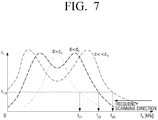
- FIG. 7 is a view showing an example of frequency scanning for determining a distance between a transmission unit and a receiving unit during initial driving
- FIG. 8 is an overall circuit diagram of an IPTS to which constant power output control through frequency variation is applied
- FIG. 9 is a view showing output power characteristics at operating frequency changes
- FIG. 10 is a diagram showing an operating frequency that satisfies target power when a distance between a transmission unit and a receiving unit changes, and the efficiency thereof;
- FIG. 11 is an overall circuit diagram of an IPTS to which constant power output control is applied using a DC-DC converter
- FIG. 13 is a final equivalent circuit diagram when assuming a transmission unit and a receiving unit are fully resonant
- FIG. 14 is a view showing internal resistance characteristic and output power characteristic in accordance with an internal resistance change when a distance between a transmission unit and a receiving unit changes;
- FIGS. 15 to 17 are views illustrating an efficiency graph by load resistance for target power satisfaction when a distance between a transmission unit and a receiving unit changes;
- FIG. 18 is a view showing load resistance and efficiency for target power satisfaction when a distance between a transmission unit and a receiving unit changes;
- FIG. 19 is a view illustrating a convertible high-frequency inverter
- FIG. 20 is a view illustrating an example of operating an inverter in FIG. 19 using a full-bridge method or a half-bridge method;
- FIG. 21 is a flowchart showing a process for driving an electronic apparatus according to a first example embodiment of the present disclosure
- FIG. 22 is a flowchart showing a process for driving a display apparatus according to an embodiment of the present disclosure.
- FIG. 23 is a flowchart showing a process for driving an electronic apparatus according to a second example embodiment of the present disclosure, and a distance measuring process.
- FIG. 1 is a view illustrating an image processing system capable of transmitting and receiving wireless power according to an embodiment of the present disclosure.
- an image processing system 90 may include a sound output apparatus 100 and a display apparatus 110 .
- the sound output apparatus 100 may include a wireless power transmission apparatus according to an embodiment of the present disclosure.
- the sound output apparatus 100 may be a peripheral apparatus disposed in the vicinity of the display apparatus 110 , and replaced with various apparatuses such as a set-top box (STB), a BD reproducer, an access point (AP), etc.
- the sound output apparatus 100 may be connected to power plug where a power line provides commercial power (e.g. commercial power ranging from 85V to 265V), and the sound output apparatus 100 may convert the commercial power into a voltage required for the display apparatus 110 and stably transmit the voltage to the display apparatus 110 .
- a power line provides commercial power (e.g. commercial power ranging from 85V to 265V)
- the sound output apparatus 100 may convert the commercial power into a voltage required for the display apparatus 110 and stably transmit the voltage to the display apparatus 110 .
- it is preferable that the display apparatus 100 uses power of DC 200V and 150 W.
- the display apparatus 110 may be disposed from the sound output apparatus 100 by a predetermined distance (e.g. within a range between 10 cm and 70 cm) so that power may be efficiently transmitted in a specific space.
- the sound output apparatus 100 may perform initial driving for transmitting power to the display apparatus 110 according to a distance (d) between two apparatuses. In other words, the sound output apparatus 100 may perform a setting operation process between two apparatuses.
- the sound output apparatus 100 may measure a distance between two apparatuses, and as a result of measurement, if the measured distance is within a predetermined range, i.e. a threshold distance, may perform an operation in connection with the display apparatus 110 . However, if the measured distance is too short, voltage gain between the transmission unit and the receiving unit may be reduced by a frequency splitting phenomenon. The sound output apparatus 100 may notify the display apparatus 110 that the voltage gain is reduced, and the display apparatus 110 may adjust a duty ratio of a DC/DC converter which operates in a PWM method to compensate the reduced voltage gain. The detailed description thereof will be made later.
- the sound output apparatus 100 may use a Convertible High-Frequency Inverter driving method instead of adjusting a frequency/duty ratio. For example, a half-bridge inverter may be changed into a full-bridge inverter.
- the display apparatus 110 may include a wireless power receiving apparatus.
- the wireless power receiving apparatus may receive power transmitted wirelessly from the wire power transmission apparatus and operate the display apparatus 110 .
- the wireless power receiving apparatus may adjust a duty ratio when PWM control of a DC/DC converter is performed according to a distance from the wireless power transmission apparatus.
- the display apparatus 110 may adjust a duty/frequency of a converter to achieve target power by varying a resistance value of a load resistance (or an effective resistance).
- a load resistance or an effective resistance.
- the above operations are not particularly limited as to what manner of operation is to be performed.
- the wireless power receiving unit may be capable of high efficiency operation and constant power control in a wide range of distances even when the distance is short.
- an image process system 90 may stably transmit power regardless of the distance between the wireless power transmission apparatus and the wireless power receiving apparatus.
- FIG. 2 is a view illustrating an image processing system according to another embodiment of the present disclosure.
- an image processing system 190 may include an image relay apparatus 200 and a display apparatus 210 .
- the image relay apparatus 200 may be a peripheral apparatus such as a set-top box (STB), a Blue-ray (BD) reproducer, or a relay apparatus (e.g. AP).
- STB set-top box
- BD Blue-ray
- AP relay apparatus
- the image relay apparatus 200 may be referred to as a power transmission apparatus.
- the image relay apparatus 200 may include an interface unit 201 and a wireless power transmission unit 203 as a set-top box.
- the interface unit 201 may convert image data input from an outside to correspond to resolution of the display apparatus 210 and output the data as an image board such as a graphic card.
- the image data may be video data of R, G and B of 8 bits or more
- the interface unit 210 may generate control signals such as a clock signal (DCLK), a vertical synchronization signal Vsync, and a horizontal synchronization signal Hsync, which correspond to the resolution of the display apparatus 210 .
- the interface unit 201 may provide the vertical/horizontal synchronization signals and the image data to the controller 211 .
- Data may be wirelessly transmitted from the interface unit 201 to the controller 211 , but also may be transmitted in a wired manner, for example, using a USB cable. Therefore, an embodiment of the present disclosure is not limited thereto.
- the interface unit 201 may include a tuner for receiving a specific broadcasting program provided by a broadcasting station, a demodulator for demodulating image signals input by the tuner, a demultiplexer for separating the demodulated image signal into video/audio data and additional information, a decoder for decoding the separated video/audio data, an audio processing unit for converting the decoded audio data into a format suitable for a speaker, and a controller (e.g. MCU) for controlling the overall operations thereof.
- a tuner for receiving a specific broadcasting program provided by a broadcasting station
- a demodulator for demodulating image signals input by the tuner
- a demultiplexer for separating the demodulated image signal into video/audio data and additional information
- a decoder for decoding the separated video/audio data
- an audio processing unit for converting the decoded audio data into a format suitable for a speaker
- a controller e.g. MCU
- the wireless power transmission unit 203 may generate a voltage required for the display apparatus 210 by using commercial power within a range from 85V to 265V. In addition, the wireless power transmission unit 203 may transmit the generated voltage to the display 210 , more specifically, to the wireless power receiving unit 216 wirelessly. Power transmission means that power of the wireless power transmission unit 203 is generated or changed rather than that actual information is transmitted. For example, it is the same principle that an inductive electromotive force is generated in the second coil when a current flows in the first coil (or an inductor) of an electric transformer.
- the wireless power transmission unit 203 may perform an operation depending on the position where the image relay apparatus 200 and the display apparatus 210 are installed by a user. That is, the wireless power transmission unit 203 , if the wireless power transmission unit 203 and the wireless power receiving unit 216 are within a predetermined range, may transmit a first voltage to the wireless power receiving unit 216 , and if both are output of the range, may transmit a second voltage.
- the display apparatus 210 may include a controller 211 , a scan driver 212 , a data driver 213 , a display panel 214 , a discharge performing unit 215 and a wireless power receiving unit 216 .
- the expression “including part or all” means that the scan driver 212 and/or the data driver 213 may be combined with (e.g. a COG method) or integrated with (e.g. AMOLED, etc.) the display panel 214 , or the discharge performing unit 215 may be omitted to form the display apparatus 210 .
- the display apparatus 210 includes all of the above components to convey full interpretation of the present disclosure.
- the controller 211 may generate control signals for controlling the scan driver 212 and the data driver 213 to display image data of RGB input through the interface unit 201 on the display panel 214 .
- the controller 211 may express the grayscale information of R, G, and B data using a logic voltage Vlog provided by the wireless power receiving unit 216 .
- Vlog provided by the wireless power receiving unit 216 .
- 8-bit information ‘10001001’ may be generated by expressing 3.3V as 1 and OV as 0.
- the controller 211 may generate a gate shift clock (GSC) signal, a gate output enable (GOE) signal, and a gate start pulse (GSP) signal as gate control signals for controlling the scan driver 212 .
- GSC gate shift clock
- GOE gate output enable
- GSP gate start pulse
- the GSC signal may be a signal for determining a time when a switching element connected to a light emitting element such as R, G, and B LED (or OLED) is turned on/off
- the GOE signal may be a signal for controlling the output of the scan driver 212
- the GSP signal may be a signal that indicates the first driving line of a screen from one vertical synchronization signal.
- the controller 211 may also generate a source sampling clock (SSC) signal, a source output enable (SOE) signal, and a source start pulse (SSP) signal as a data control signal.
- SSC source sampling clock
- SOE source output enable
- SSP source start pulse
- the SSC signal may be used as a sampling clock for latching data in the data driver 230
- the SOE signal may transfer the data latched by the SSC to the display panel 214 .
- the SSP signal may be a signal for notifying the start of data latching or sampling during one horizontal synchronization period.
- the controller 211 may process data signals, serial data shift clock (S CLK), LAT, and grayscale (GS) pulse width modulation (PWM) reference clock (G CLK) with the IC.
- the data signal may be grayscale data of R, G, and B.
- the S CLK signal may be a signal for shifting data input to the data driver 213 to a shift register (e.g. 48-bit common shift register (MSB)) in synchronization with the rising edge of the S CLK.
- the data stored in the shift register may be shifted from each S CLK rising edge to the MSB.
- the LAT may be a signal for latching data at the falling edge from the MSB to a memory (ex. GS data memory).
- the G CLK may be a signal for increasing the GS counter by one on each rising edge of G CLK for PWM control.
- the controller 211 may include a control signal generation unit (not shown) and a data rearrangement unit (not shown).
- the control signal generation unit if a time for displaying an image in a unit frame on the display panel 214 is 16.7 ms, may generate a control signal to display a unit frame image within a predetermined time.
- the data rearrangement unit may reproduce the input RGB image data to be suitable for the display panel 214 .
- the controller 211 may convert 8 bit data into 64 bit data.
- the scan driver 212 may receive a gate-on voltage (Vdd) and a gate-off voltage (Vss) provided by the wireless power receiving unit 216 and apply the voltage to the display panel 214 under the control of the controller 211 .
- the gate-on voltage (Vdd) may be provided from a second line 1 (GL1) to a scan line N (GLn) sequentially to embody a unit frame image on the display panel 214 .
- the scan driver 212 may operate in response to the scan signal generated by the controller 211 according to an embodiment of the present disclosure.
- the scan driver 212 may include a power voltage source and a switching element connected to each scan line as shown in FIG. 2 .
- the switching element may use not only a TFT element, but also a transistor (TR) and MOSFET.
- the data driver 213 may convert video data of R, G and B provided serially by the controller 211 into video data in parallel, convert digital data into an analogue current or a duty-on current (e.g. a pulse current), and provide video data corresponding to a single horizontal line on the display panel 214 for each horizontal line simultaneously and sequentially.
- Digital information of video data provided by the controller 211 may be converted into an analogue current including a color grayscale and the analogue current may be provided to the display panel 214 .
- the analog current may be a pulse type current. It is preferable that the data driver 213 may also be synchronized with a gate signal provided to the scan driver 212 and output unit frame data.
- the data driver 213 may be variably configured depending on whether a light emitting element is driven with a constant current, or with a constant voltage.
- the Texas Instruments TLC5958 Series IC may be used for the data driver 213 .
- the display panel 214 may include a plurality of scan lines and a plurality of data lines intersecting with each other to define a pixel area, and light emitting elements of R, G and B such as LED (or OLED) may be provided in the pixel area where the scan lines and the data lines cross each other.
- light emitting elements may generate a current corresponding to their grayscale information through the data lines connected to the scan lines to which a power voltage is supplied.
- the display panel 214 may display an image by adjusting brightness depending on the amount of charge flowing through a current path.
- the light emitting element may be driven by a constant voltage. Therefore, an embodiment of the present disclosure is not limited thereto.
- the discharge performing unit 215 may discharge parasitic charge by a parasitic capacitor of each scan line to a ground when each scan line discharges.
- the discharge performing unit 215 may be controlled by the controller 211 .
- the discharge performing unit 215 may be controlled between when the power voltage Vdd provided to a scan line 1 is blocked, and when a power voltage is provided to a scan line 2.
- the wireless power receiving unit 216 may allow the display apparatus 210 to use constant power regardless of the distance from the wireless power transmission unit 203 . Therefore, while being linked to the wireless power transmission unit 203 , if the distance from the wireless power transmission unit 203 is within a predetermined range, the duty ratio of the inverter may not be changed. However, if the distance is output of the predetermined range, the duty ration may be changed. For example, if the distance between the wireless power transmission unit 203 and wireless power receiving unit 216 is too short, voltage gain may between the transmission unit and the receiving unit may be significantly lowered. Therefore, it is preferable that the wireless power transmission unit 203 changes a driving method of the inverter.
- the wireless power receiving unit 216 may generate a first voltage (e.g. DC 200V) and a second voltage (e.g. DC 13V) through a converter and provide the generated voltage to each functional block (e.g. a display panel, a driver, etc.).
- the wireless power receiving unit 216 may generate a voltage of DC 3.3V as a logic voltage to present a grayscale for the controller 211 , and generate various magnitudes of voltages such as a voltage of DC 4.5V as a gate-on voltage Vdd for the scan driver 220 .
- the wireless power receiving unit 216 may generate a VCC voltage (e.g. DC13V), which is input to an IC, when the controller 211 , the scan driver 212 , and the data driver 213 are integrated in IC form.
- a VCC voltage e.g. DC13V
- FIG. 3 is a block diagram exemplifying a detailed structure of a wireless power transmission unit shown in FIG. 2 .
- a wireless power transmission unit 203 may include part or all of a filter 300 , a PFC unit 310 , a converter 320 , a switching unit 330 , a regulator 340 , a controller 350 , an inverter 360 , a resonance circuit unit 370 , and a first coil unit 380 .
- the wireless power transmission unit 203 may be a stand-alone type individual apparatus, and the expression “include part or all” means that some constituent elements are omitted. However, it will be assumed that the wireless power transmission unit 203 includes all of the above components to convey full interpretation of the present disclosure.
- the filter 300 may rectify or smooth the input commercial power and output a DC voltage at a constant level.
- a half-wave or full-wave rectifier circuit may be used for rectification, and a capacitor may be connected to an output end of the rectifier circuit in parallel for smoothing.
- the PFC unit 310 may change the voltage output from the filter 300 to a voltage of 400V through a converter to output.
- the PFC unit 310 may include a fly-back converter.
- the converter 320 may be provided with a smoothing voltage output from the filter 300 , generate a DC voltage of 13V, and provide the DC voltage to the switching unit 330 and the regulator 340 .
- the switching unit 330 may output a first voltage of DC 13V and a second voltage of DC 400V, which is selected under the control of the first controller 350 .
- the regulator 340 may perform an operation for proving a stable voltage to the first controller 350 .
- the regulator 340 may allow the ripple to be improved in the output voltage.
- the controller 350 may measure a distance between the image relay apparatus 220 and the display apparatus 210 automatically or by a command of a system designer or a user, more specifically, a distance between the wireless power transmission unit 203 and the wireless power receiving unit 216 of FIG. 2 .
- the first controller 350 may control the switching unit 330 and output a voltage of DC 13V to the inverter 360 .
- the voltage of DC 13V may be a voltage for measuring a distance.
- the first controller 350 may sense a current of the inverter 360 and measure a distance between two apparatuses. For example, the first controller 350 may determine whether a current value of the sensed current coincides with the stored current value, and then determine an operating frequency and a distance.
- a frequency corresponding to a peak of a resonance point may be found based on a current value sensed by gradually increasing the operating frequency, and the pre-stored optimal operating frequency/duty corresponding to the frequency may be set as the initial operating condition of the inverter.
- the first controller 350 may perform down-scanning or up-scanning for measuring a distance.
- the down-scanning comprises gradually reducing the frequency while operating the wireless power transmission apparatus 203 with the maximum frequency within a predetermined range, determining the frequency at a time when a current is sensed, and determining a distance.
- the controller 350 may determine the distance based on the pre-stored distance information matched with the frequency.
- the first controller 350 may measure the distance in the up-scanning method.
- the up-scanning method comprises identifying a point where the current value is maximum by sequentially increasing the operating frequency within the given range, i.e. determining the distance through the determined maximum current value.
- the method comprises finding and determining the distance information matched with the maximum current value.
- the first controller 350 may control the switching unit 330 so that the voltage of DC 400V may be output to the inverter 360 . As a result, a wireless power operation may start.
- the inverter 360 may convert the input voltage of DC 400V into an AC voltage to output.
- the inverter 360 may include a PWM circuit to enable PWM control by the first controller 350 .
- the first controller 350 may control the inverter 360 and adjust an operating frequency and a duty-on time, and when the distance measurement is completed, the inverter 360 may operate with the determined operating frequency and duty ratio at fixed values.
- the PWM circuit is well-known in the art, and thus further description will be omitted.
- the inverter 360 according to an embodiment of the present disclosure includes a convertible high-frequency inverter.
- the inverter 360 may drive a full-bridge type inverter or a half-bridge type inverter depending on the distance.
- the full-bridge type inverter may further include a switching element compared to the half-bridge type inverter. Therefore, according to an embodiment, the inverter 360 may be conveniently driven using the half-bridge method by driving switching elements corresponding to one pole in the full-bridge method.
- a Zero Voltage Switching (ZVC) unit 370 may include a ZVC element (filter). Such the ZVC unit 370 may operate when a distance between the wireless power transmission unit 203 and the wireless power receiving unit 216 is small. As the distance between the wireless power transmission unit 203 and the wireless power receiving unit 216 is reduced, gain for power transmission may be reduced. As a result, the display apparatus 210 may not obtain the desired power.
- the zero voltage may generate when a distance (e.g. 30 cm) becomes too short, and the coil of the first coil unit 380 may be affected by the coil of the second coil unit 400 , so that mutual inductance may increase, and a current may fail to flow through the first coil. As a result, power may not be properly transmitted.
- the ZVS unit 370 may constantly maintain the efficiency of power transmission by allowing a current to flow through the ZVS element.
- the first coil unit 380 may include a coil, i.e. an inductor, a current may flow through a first coil, and thus an inductive electromotive force may be generated in the wireless power receiving unit.
- FIG. 4 is a block diagram exemplifying a detailed structure of a wireless power transmission unit shown in FIG. 2 .
- the wireless power receiving unit 216 may include some or all of a second coil unit 400 , a rectifier 410 , a smoothing circuit 420 , a converter 430 , an overvoltage detector 440 , a second controller 450 and a switching unit 460 .
- the expression “include part or all” means that the overvoltage detector 440 is omitted or some constituent elements are integrated with other constituent elements. However, it will be assumed that the wireless power receiving unit 216 includes all of the above components to convey full interpretation of the present disclosure.
- the second coil unit 400 may include a coil, that is, an inductor, and the inductive electromotive force may be generated by a voltage applied to the first coil unit 380 of the wireless power transmission unit 203 and a current which flows through the first coil.
- Such inductive electromotive force may have a unit of voltage.
- the rectifier 410 and the smoothing circuit 420 may rectify and smooth the AC voltage provided by the second coil unit 400 and convert the AC voltage into the DC voltage.
- the converter 430 may include a DC-DC converter, and generate and output voltages of DC 200V and DC 13V.
- the voltage of DC 200V may be provided to drive an LED string provided in the display panel 214 .
- the voltage of DC 13V may be used as a VCC power source of the controller 211 , or the scan driver 212 and the data driver 213 .
- PWM control may be performed on the DC-DC converter constituting the converter 430 , and the duty ratio may be adjusted according to the distance.
- the converter 430 may operate in three manners. In other words, when the operating frequency of the inverter 360 is determined based on the distance, the wireless power transmission unit 203 may operate with a predetermined duty without additional duty adjustment. If the operating frequency of the inverter 360 is constant regardless of the distance, the converter 430 may operate by adjusting the duty according to the distance. The converter 430 may measure the distance by sensing the current output from the converter 430 and comparing the output current with a predetermined value, and adjust the duty by using pre-stored duty information, which is matched with the measured distance. Further, when the distance is too short, it is possible to adjust the duty with changing the operating frequency of the inverter.
- the overvoltage detector 440 may detect the overvoltage applied from the second coil unit 440 to the rectifier 410 and transmit the overvoltage to the second controller 450 .
- the second controller 450 may temporarily block the voltage applied to the rectifier 410 .
- the second controller 450 may control the converter 430 upon the request of the wireless power transmission unit 203 . For example, if it is determined that the converter unit 430 needs to adjust the duty ratio as the internal resistance increases, the second controller 450 may adjust the duty ratio nu controlling the converter 430 .
- the second controller 450 may maintain the switching unit 460 to be turned off so that the voltage of DC 13V may not be output during the initial driving, or the scanning operation for measuring the distance after the image replay apparatus 200 and the display apparatus 210 are installed. When it is determined that the scanning operation is completed by sensing the current output from the converter 430 .
- the switching unit 460 may be turned on and the voltage of DC 13V may be output.
- the wireless power receiving unit 216 may generate a stable voltage required by the display apparatus 210 .
- the stable voltage may affect the image quality of the display panel 214 .
- FIG. 5 is a view illustrating output power and efficiency characteristic according to a distance change of a voltage source input inductive power transfer system (IPTS).
- IPTS voltage source input inductive power transfer system
- d dc may be a weak region
- d dc may be a strong region
- the frequency separation phenomenon may significantly occur in the strong region.
- output power (P L ) may be maintained the same as the target power when the distance between the wireless power transmission unit 203 and the wireless power receiving unit 216 changes in a wide range (in the storing region and the weak region), and high efficiency may be achieved at the same time.
- the load connected to the wireless power receiving unit 216 e.g. home appliance such as a TV, a microwave, a computer, a monitor, etc.
- the magnitude and the phase of impedance reflected from the wireless power receiving unit 216 to the wireless power transmission unit 203 may vary depending on the distance due to a parallel capacitor Cp of the wireless power receiving unit 216 when the distance between the wireless power receiving unit 216 to the wireless power transmission unit 203 changes.
- the distance between the wireless power receiving unit 216 and the wireless power transmission unit 203 may be indirectly determined without an additional communication circuit, and the distance may also be determined through up-scanning.
- FIG. 7 is a view showing an example of frequency scanning for determining a distance between a transmission unit and a receiving unit during initial driving.
- a distance between the wireless power transmission unit 203 and the wireless power receiving unit 216 through frequency scanning may be determined by the first controller 350 of FIG. 3 .
- circuit diagram (a) of FIG. 6 When the distance between the wireless power receiving unit 216 and the wireless power transmission unit 203 changes, the resonance point of the impedance from the wireless power transmission unit 203 to the wireless power receiving unit 216 may be changed (refer to circuit diagram (a) of FIG. 6 ), so that the magnitude of the current of the wireless power transmission unit 203 may vary depending on the operating frequency (refer to circuit diagram (b) of FIG. 6 ).
- Circuit diagrams (a) and (b) of FIG. 6 are respectively expressed by ⁇ Equation 1> and ⁇ Equation 2> as follows.
- the wireless power receiving unit 216 may be equivalently self-coupled to the wireless power transmission unit 203 .
- the distance between the wireless power transmission unit 203 and the wireless power receiving unit 216 during the initial driving may be determined by measuring an operating frequency (e.g. fs 1 , fs 2 , fs 3 , etc.) at which a current I 1 of the wireless power transmission unit 203 reaches a current I 1,s of a predetermined magnitude (refer to FIG. 7 ).
- This feature refers to a down-scanning method according to an embodiment of the present disclosure.
- the distance corresponding to the sensed operating frequency may be indirectly determined.
- the wireless power transmission unit 203 may use an up-scanning method in addition to a down-scanning method for measuring a distance.
- the wireless power transmission unit 203 may apply a voltage of 13V during scanning and identify the weak/storing region by using frequency information corresponding to a peak point of the first resonance frequency, that is, a point at which a current value is maximum.
- the DC-DC converter 430 may operate in the area ranging from 100V to 400V, and the MCU of the wireless power receiving unit 216 , i.e. the second controller 450 may output a voltage of 13V when operating within a normal input voltage range of DC-DC output. Therefore, when a normal voltage is output and power becomes stable, the switching unit 460 may be turned on or turned off.
- the wireless power transmission unit 203 may transmit power of 150 W when a voltage of 400V is applied.
- the optimum efficiency may be achieved by not supplying excess power to the wireless power receiving unit 216 more than necessary.
- a switching circuit may be turned off to protect an apparatus when an overvoltage (or an overcurrent) is applied, and may perform additional functions to protect the load.
- FIG. 8 is an overall circuit diagram of an IPTS to which constant power output control through frequency variation is applied
- FIG. 9 is a view showing output power characteristics at operating frequency changes
- FIG. 10 is a diagram showing an operating frequency that satisfies target power when a distance between a transmission unit and a receiving unit changes, and the efficiency thereof.
- the inverter 360 may operate at the second frequency (inductive region).
- the inverter 360 may operate at the third or fourth frequency (inductive region).
- constant power output control may become possible while operating with a frequency that satisfies target power (refer to FIG. 10 ).
- the frequency in the inductive region of FIG. 9 may be used.
- the ZVS operation may be guaranteed.
- FIG. 11 is an overall circuit diagram of an IPTS to which constant power output control is applied using a DC-DC converter
- FIG. 13 is a final equivalent circuit diagram when assuming a transmission unit and a receiving unit are fully resonant
- FIG. 14 is a view showing internal resistance characteristic and output power characteristic according to an internal resistance change when a distance between a transmission unit and a receiving unit changes.
- constant power output control may be possible in accordance with an effective resistance change when the DC-DC converter's duty of the wireless power receiving unit 216 varies.
- Equation 1 a final equivalent circuit in the complete resonance of the wireless power transmission unit 203 and the wireless power receiving unit 216 is expressed by Equation
- constant power output control may be possible by varying an effective resistance Re of output side (refer to FIG. 14 ).
- FIG. 14 is explained as follows.
- FIGS. 15 to 17 are views illustrating an efficiency graph by load resistance for target power satisfaction when the between the transmission unit and the receiving unit changes.
- the operation may be performed at one effective resistance (load resistance) operating point that satisfies target power in the weak region.
- a greater effective resistance between two points in the storing region may be significantly out of the operating range of the DC/DC converter, and thus efficiency thereof may be low.
- FIG. 18 is a view showing load resistance and efficiency for target power satisfaction when a distance between a transmission unit and a receiving unit changes
- FIG. 19 is a view illustrating a convertible high-frequency inverter
- FIG. 20 is a view illustrating an example of operating an inverter in FIG. 19 using a full-bridge method or a half-bridge method.
- the distance between the wireless power transmission unit 203 and the wireless power receiving unit 216 may be determined by using only the current information of the wireless power transmission unit 203 , and by applying the optimal operating frequency according to the distance determination, constant power output control may be possible even in the change of the distance in the wide range without a complicated control circuit (e.g. a frequency variance control method).
- a complicated control circuit e.g. a frequency variance control method
- constant power output control may be possible even in the change in distance in the wide range (e.g. a method for controlling a DC/DC converter).
- FIG. 21 is a flowchart showing a process for driving an electronic apparatus (e.g. a sound output apparatus, an image replay apparatus, etc.) according to a first example embodiment of the present disclosure.
- an electronic apparatus e.g. a sound output apparatus, an image replay apparatus, etc.
- an electronic apparatus 100 and 200 may be linked to a display apparatus 110 and 210 to perform at least one of video data or audio data at step S 2100 .
- audio data may be processed
- video data and audio data may be processed.
- the electronic apparatus 100 and 200 may operate the inverter with the operating frequency determined depending on the distance between the electronic apparatus 100 and 200 and the display apparatus 110 and 210 , a DC voltage input to the outside (corresponding to the DC voltage converted from the AV voltage) may be converted into the AC voltage, and the inductive electromotive force may be generated in the display apparatus by the AC voltage at step S 2110 .
- FIG. 22 is a flowchart showing a process for driving a display apparatus according to an embodiment of the present disclosure.
- the display apparatus 110 and 210 may generate a voltage corresponding to the inductive electromotive force generated by the external apparatus located at a predetermined distance, for example, the electronic apparatus 100 and 200 , rectify the generated voltage with a resonance frequency determined based on the distance, and adjust the rectified voltage through the duty variance of the converter to output the rectified voltage as a target voltage at step S 2210 .
- the display apparatus 110 and 210 may display an image on a display panel by using a target voltage at step S 2200 .
- FIG. 23 is a flowchart showing a process for driving an electronic apparatus according to a second example embodiment of the present disclosure, and a distance measuring process.
- the electronic apparatus 100 and 200 may store the operating frequency and the current value (or information) in accordance with the distance from the display apparatus 110 and 210 at step S 2300 .
- the current value may include a maximum current value.
- the electronic apparatus 100 and 200 may transmit the voltage generated in accordance with the change of the operating frequency during the initial driving after being installed in a random space to the display apparatus 110 and 210 in a wireless manner at step 2310 .
- the expression “transmit in a wireless manner” means generating the inductive electromotive force in the display apparatus 110 and 210 by the voltage generated by the electronic apparatus 100 and 200 .
- the electronic apparatus 100 and 200 may sense a current value according to the changed operating frequency at step S 2320 . Accordingly, the maximum current value may be sensed at a specific frequency.
- the electronic apparatus 100 and 200 may identify the operating frequency when the sensed current value coincides with the stored current value, for example, when the sensed maximum current value coincides with the stored current value at step S 2330 .
- the electronic apparatus 100 and 200 may determine the distance accordingly. That is, the distance may be determined by confirming the operating frequency and current value, which are matched with the distance and stored for determination.
- the wired line can be eliminated and visually good in the interior design aspect.
- the non-transitory computer readable medium refers to a medium that stores data semi-permanently rather than storing data for a very short time, such as a register, a cache, and a memory, and is readable by an apparatus.
- a non-transitory computer readable medium such as a compact disc (CD), a digital versatile disk (DVD), a hard disk, a Blu-ray disk, a universal serial bus (USB) memory stick, a memory card, and a read only memory (ROM), and may be provided.
Landscapes
- Engineering & Computer Science (AREA)
- Power Engineering (AREA)
- Computer Networks & Wireless Communication (AREA)
- Physics & Mathematics (AREA)
- Computer Hardware Design (AREA)
- General Physics & Mathematics (AREA)
- Theoretical Computer Science (AREA)
- Control Of Indicators Other Than Cathode Ray Tubes (AREA)
- Control Of El Displays (AREA)
Abstract
Description
and thus an overcharge η is expressed by <Equation 3> as follow.
Xr(Re)Xm 2+Xr(Re) [Equation 3]
Claims (14)
Applications Claiming Priority (3)
| Application Number | Priority Date | Filing Date | Title |
|---|---|---|---|
| KR10-2016-0090742 | 2016-07-18 | ||
| KR1020160090742A KR102622053B1 (en) | 2016-07-18 | 2016-07-18 | Electronic Apparatus, Display Apparatus, and Driving Method Thereof |
| PCT/KR2017/006593 WO2018016751A1 (en) | 2016-07-18 | 2017-06-22 | Electronic apparatus and display apparatus, and method for operating apparatuses |
Publications (2)
| Publication Number | Publication Date |
|---|---|
| US20190157910A1 US20190157910A1 (en) | 2019-05-23 |
| US11088571B2 true US11088571B2 (en) | 2021-08-10 |
Family
ID=60993169
Family Applications (1)
| Application Number | Title | Priority Date | Filing Date |
|---|---|---|---|
| US16/318,492 Active US11088571B2 (en) | 2016-07-18 | 2017-06-22 | Electronic apparatus and display apparatus, and method for operating apparatuses |
Country Status (4)
| Country | Link |
|---|---|
| US (1) | US11088571B2 (en) |
| EP (1) | EP3451493A4 (en) |
| KR (1) | KR102622053B1 (en) |
| WO (1) | WO2018016751A1 (en) |
Cited By (1)
| Publication number | Priority date | Publication date | Assignee | Title |
|---|---|---|---|---|
| US11144159B2 (en) * | 2020-11-30 | 2021-10-12 | Shanghai Tianma AM-OLED Co., Ltd. | Driving method of display panel, display panel and display device |
Families Citing this family (19)
| Publication number | Priority date | Publication date | Assignee | Title |
|---|---|---|---|---|
| KR20190090918A (en) * | 2018-01-26 | 2019-08-05 | 엘지이노텍 주식회사 | Adaptive Wireless Power Reception Method and Apparatus |
| KR20200030407A (en) | 2018-09-12 | 2020-03-20 | 삼성전자주식회사 | Display system, display apparatus and control method thereof |
| JP2020065388A (en) * | 2018-10-18 | 2020-04-23 | セイコーエプソン株式会社 | Control unit, power transmission device, non-contact power transmission system, power receiving device, and electronic apparatus |
| CN109639259B (en) * | 2018-12-05 | 2022-07-22 | 惠科股份有限公司 | Method for spreading spectrum, chip, display panel and readable storage medium |
| KR20200101237A (en) | 2019-02-19 | 2020-08-27 | 삼성전자주식회사 | Device for wireless power transmission and operating method thereof |
| KR102566800B1 (en) * | 2019-05-31 | 2023-08-16 | 엘지전자 주식회사 | display device |
| KR102646067B1 (en) * | 2019-07-17 | 2024-03-12 | 삼성전자주식회사 | Electronic apparatus, control method thereof and display apparatus |
| JP2021033222A (en) * | 2019-08-29 | 2021-03-01 | 凸版印刷株式会社 | Information display device, control method for information display device, display control device, and electronic paper display device |
| IT201900021480A1 (en) * | 2019-11-18 | 2021-05-18 | Amper Auto S R L | SYSTEM AND PROCEDURE FOR THE CONTROL OF THE ELECTRIC POWER IN GALVANICALLY INSULATED LOADS FROM THE POWER SOURCE, IN PARTICULAR FOR NAUTICAL APPLICATIONS |
| WO2021124459A1 (en) * | 2019-12-17 | 2021-06-24 | 三菱電機株式会社 | Power conversion system |
| US11676529B2 (en) * | 2019-12-23 | 2023-06-13 | Intel Corporation | Methods and apparatus for in-pixel driving of micro-LEDs |
| CN111371294B (en) * | 2020-04-03 | 2021-04-30 | 宁波安信数控技术有限公司 | Frequency spectrum shifting MOS drive circuit and method based on digital amplitude modulation technology |
| KR20210136576A (en) * | 2020-05-08 | 2021-11-17 | 삼성전자주식회사 | Electronic apparatus and control method thereof |
| KR20220005959A (en) * | 2020-07-07 | 2022-01-14 | 삼성전자주식회사 | Electronic device for wirelessly receiving power and method for operating thereof |
| WO2022025309A1 (en) * | 2020-07-28 | 2022-02-03 | 엘지전자 주식회사 | Display apparatus and power controlling method therefor |
| CN112290696A (en) * | 2020-10-27 | 2021-01-29 | 济南大学 | Wireless power transmission system and method capable of inhibiting frequency splitting phenomenon |
| KR102517706B1 (en) * | 2021-03-17 | 2023-04-03 | 전남대학교산학협력단 | Apparatus, method and program for transmitting and receiving wireless power |
| EP4084283A1 (en) | 2021-04-27 | 2022-11-02 | Wiferion GmbH | Wireless power transmission device for inductive electric power transmission and method for operating the power transmission device for supporting zero-voltage switching |
| WO2023149773A1 (en) * | 2022-02-04 | 2023-08-10 | 주식회사 와이파워원 | Multi-phase feeding device for wireless power transmission and method of controlling same |
Citations (19)
| Publication number | Priority date | Publication date | Assignee | Title |
|---|---|---|---|---|
| US20110109263A1 (en) | 2009-11-09 | 2011-05-12 | Kabushiki Kaisha Toyota Jidoshokki | Resonance type non-contact charging apparatus |
| US20110254377A1 (en) * | 2010-04-08 | 2011-10-20 | Qualcomm Incorporated | Wireless power transmission in electric vehicles |
| KR20120005112A (en) | 2010-07-08 | 2012-01-16 | 삼성전자주식회사 | Adaptive wireless power transmit apparatus and method for mobile device in wireless power transmission systems |
| US20120025627A1 (en) | 2010-07-28 | 2012-02-02 | Semiconductor Energy Laboratory Co., Ltd. | Wireless power feeding system and wireless power feeding method |
| WO2012045050A2 (en) | 2010-09-30 | 2012-04-05 | Intel Corporation | Wireless power transfer apparatus and method thereof |
| KR20120066281A (en) | 2010-12-14 | 2012-06-22 | 삼성전기주식회사 | Wireless power transmission apparatus and transmission method thereof |
| US20130033117A1 (en) | 2011-08-05 | 2013-02-07 | Samsung Electronics Co., Ltd. | Wireless power transmission system, and method and apparatus for controlling power in wireless power transmission system |
| US20130300210A1 (en) * | 2011-01-26 | 2013-11-14 | Murata Manufacturing Co., Ltd. | Power transfer system |
| KR20140007273A (en) | 2012-07-09 | 2014-01-17 | 엘지전자 주식회사 | Wireless power transfer method, apparatus and system |
| KR101390954B1 (en) | 2012-12-18 | 2014-04-29 | 한국과학기술원 | Wireless power receiving apparatus with automatic load resistance modulation for efficiency and power improvement |
| CN203744088U (en) | 2013-11-25 | 2014-07-30 | 欧阳伟峰 | Multifunctional desk lamp |
| KR20140121200A (en) | 2013-04-05 | 2014-10-15 | 엘지전자 주식회사 | Wireless power receiving apparatus and wireless power transmitting/receiving apparatus |
| US20140368053A1 (en) * | 2012-01-25 | 2014-12-18 | Lg Electronics Inc. | Method and apparatus for setting frequency of wireless power transmission |
| US20150077051A1 (en) | 2013-09-13 | 2015-03-19 | Samsung Electronics Co., Ltd. | Method of power transmitting unit (ptu) for determining location of power receiving unit (pru), and ptu employing the method |
| US20150249484A1 (en) * | 2012-10-11 | 2015-09-03 | Powermat Technologies, Ltd. | Inductive power transmission system and method for concurrently transmitting digital messages |
| US20150372493A1 (en) * | 2014-06-18 | 2015-12-24 | WIPQTUS Inc. | Wireless power system for portable devices under rotational misalignment |
| US9287039B2 (en) | 2012-07-09 | 2016-03-15 | Lg Electronics Inc. | Wireless power transfer method, apparatus and system for low and medium power |
| US20160079798A1 (en) | 2014-09-11 | 2016-03-17 | Samsung Electro-Mechanics Co., Ltd. | Non-contact type charger |
| WO2016073867A1 (en) | 2014-11-07 | 2016-05-12 | Murata Manufacturing Co., Ltd. | Variable-distance wireless-power-transfer system with fixed tuning and power limiting |
Family Cites Families (1)
| Publication number | Priority date | Publication date | Assignee | Title |
|---|---|---|---|---|
| CN102439669B (en) * | 2009-02-13 | 2015-11-25 | 韦特里西提公司 | Damage the wireless energy transfer in environment |
-
2016
- 2016-07-18 KR KR1020160090742A patent/KR102622053B1/en active IP Right Grant
-
2017
- 2017-06-22 US US16/318,492 patent/US11088571B2/en active Active
- 2017-06-22 EP EP17831224.5A patent/EP3451493A4/en not_active Withdrawn
- 2017-06-22 WO PCT/KR2017/006593 patent/WO2018016751A1/en unknown
Patent Citations (32)
| Publication number | Priority date | Publication date | Assignee | Title |
|---|---|---|---|---|
| US20110109263A1 (en) | 2009-11-09 | 2011-05-12 | Kabushiki Kaisha Toyota Jidoshokki | Resonance type non-contact charging apparatus |
| US20110254377A1 (en) * | 2010-04-08 | 2011-10-20 | Qualcomm Incorporated | Wireless power transmission in electric vehicles |
| EP2889177A1 (en) | 2010-04-08 | 2015-07-01 | Qualcomm Incorporated | Wireless power transmission in electric vehicles |
| KR20120005112A (en) | 2010-07-08 | 2012-01-16 | 삼성전자주식회사 | Adaptive wireless power transmit apparatus and method for mobile device in wireless power transmission systems |
| US20120025627A1 (en) | 2010-07-28 | 2012-02-02 | Semiconductor Energy Laboratory Co., Ltd. | Wireless power feeding system and wireless power feeding method |
| US9472974B2 (en) | 2010-07-28 | 2016-10-18 | Semiconductor Energy Laboratory Co., Ltd. | Wireless power feeding system and wireless power feeding method |
| KR20130099015A (en) | 2010-07-28 | 2013-09-05 | 가부시키가이샤 한도오따이 에네루기 켄큐쇼 | Wireless power feeding system and wireless power feeding method |
| WO2012045050A2 (en) | 2010-09-30 | 2012-04-05 | Intel Corporation | Wireless power transfer apparatus and method thereof |
| KR20150104228A (en) | 2010-09-30 | 2015-09-14 | 인텔 코포레이션 | Wireless power transfer apparatus and method thereof |
| US20140333147A1 (en) | 2010-12-14 | 2014-11-13 | Samsung Electro-Mechanics Co., Ltd. | Wireless power transmission/reception apparatus and method |
| US8803365B2 (en) | 2010-12-14 | 2014-08-12 | Samsung Electro-Mechanics Co., Ltd. | Wireless power transmission/reception apparatus and method |
| KR20120066281A (en) | 2010-12-14 | 2012-06-22 | 삼성전기주식회사 | Wireless power transmission apparatus and transmission method thereof |
| US9378888B2 (en) | 2011-01-26 | 2016-06-28 | Murata Manufacturing Co., Ltd. | Power transfer system |
| JP5494838B2 (en) | 2011-01-26 | 2014-05-21 | 株式会社村田製作所 | Power transmission system |
| US20130300210A1 (en) * | 2011-01-26 | 2013-11-14 | Murata Manufacturing Co., Ltd. | Power transfer system |
| US9608452B2 (en) | 2011-08-05 | 2017-03-28 | Samsung Electronics Co., Ltd. | Wireless power transmission system, and method and apparatus for controlling power in wireless power transmission system |
| KR20130015836A (en) | 2011-08-05 | 2013-02-14 | 삼성전자주식회사 | Wireless power transmission system, method and apparatus for power control in power transmission system |
| US20130033117A1 (en) | 2011-08-05 | 2013-02-07 | Samsung Electronics Co., Ltd. | Wireless power transmission system, and method and apparatus for controlling power in wireless power transmission system |
| US20140368053A1 (en) * | 2012-01-25 | 2014-12-18 | Lg Electronics Inc. | Method and apparatus for setting frequency of wireless power transmission |
| KR20140007273A (en) | 2012-07-09 | 2014-01-17 | 엘지전자 주식회사 | Wireless power transfer method, apparatus and system |
| US9287039B2 (en) | 2012-07-09 | 2016-03-15 | Lg Electronics Inc. | Wireless power transfer method, apparatus and system for low and medium power |
| US20160172895A1 (en) | 2012-07-09 | 2016-06-16 | Lg Electronics Inc. | Wireless power transfer method, apparatus and system for low and medium power |
| US20150249484A1 (en) * | 2012-10-11 | 2015-09-03 | Powermat Technologies, Ltd. | Inductive power transmission system and method for concurrently transmitting digital messages |
| KR101390954B1 (en) | 2012-12-18 | 2014-04-29 | 한국과학기술원 | Wireless power receiving apparatus with automatic load resistance modulation for efficiency and power improvement |
| KR20140121200A (en) | 2013-04-05 | 2014-10-15 | 엘지전자 주식회사 | Wireless power receiving apparatus and wireless power transmitting/receiving apparatus |
| KR20150031357A (en) | 2013-09-13 | 2015-03-24 | 삼성전자주식회사 | Method of determining location of power receiving unit in power transmitting unit and the power transmitting unit |
| US20150077051A1 (en) | 2013-09-13 | 2015-03-19 | Samsung Electronics Co., Ltd. | Method of power transmitting unit (ptu) for determining location of power receiving unit (pru), and ptu employing the method |
| US9985458B2 (en) | 2013-09-13 | 2018-05-29 | Samsung Electronics Co., Ltd. | Method of power transmitting unit (PTU) for determining location of power receiving unit (PRU), and PTU employing the method |
| CN203744088U (en) | 2013-11-25 | 2014-07-30 | 欧阳伟峰 | Multifunctional desk lamp |
| US20150372493A1 (en) * | 2014-06-18 | 2015-12-24 | WIPQTUS Inc. | Wireless power system for portable devices under rotational misalignment |
| US20160079798A1 (en) | 2014-09-11 | 2016-03-17 | Samsung Electro-Mechanics Co., Ltd. | Non-contact type charger |
| WO2016073867A1 (en) | 2014-11-07 | 2016-05-12 | Murata Manufacturing Co., Ltd. | Variable-distance wireless-power-transfer system with fixed tuning and power limiting |
Non-Patent Citations (5)
| Title |
|---|
| Communication pursuant to Article 94(3) EPC dated May 14, 2020 in counterpart European Patent Application No. 17831224.5. |
| Extended European Search Report dated May 14, 2019 in counterpart European Patent Application No. 17831224.5. |
| International Search Report for PCT/KR2017/006593, dated Oct. 16, 2017 and English-language translation, 4 pages. |
| Ryu et al., "Novel AC Equivalent Load Modeling for Resonant DC/DC Converter with Duty Adjusting Control Scheme", The Korean Institute of Power Electronics, Jul. 13-14, 2012, 4 pages—with English Abstract. |
| Written Opinion of the ISA for PCT/KR2017/006593, dated Oct. 16, 2017 and English-language translation, 12 pages. |
Cited By (1)
| Publication number | Priority date | Publication date | Assignee | Title |
|---|---|---|---|---|
| US11144159B2 (en) * | 2020-11-30 | 2021-10-12 | Shanghai Tianma AM-OLED Co., Ltd. | Driving method of display panel, display panel and display device |
Also Published As
| Publication number | Publication date |
|---|---|
| US20190157910A1 (en) | 2019-05-23 |
| KR102622053B1 (en) | 2024-01-08 |
| EP3451493A1 (en) | 2019-03-06 |
| WO2018016751A1 (en) | 2018-01-25 |
| EP3451493A4 (en) | 2019-06-12 |
| KR20180009175A (en) | 2018-01-26 |
Similar Documents
| Publication | Publication Date | Title |
|---|---|---|
| US11088571B2 (en) | Electronic apparatus and display apparatus, and method for operating apparatuses | |
| US10938242B2 (en) | Display apparatus and operational method therefor, and electronic apparatus | |
| US10332474B2 (en) | Display apparatus having power supply device with power factor compensation and power supply method thereof | |
| US9437127B2 (en) | Device and method for displaying image, device and method for supplying power, and method for adjusting brightness of contents | |
| US9318948B2 (en) | Power circuit part, power control method thereof and display apparatus having the same | |
| US20150061530A1 (en) | Light source driving apparatus having a snubber to prevent voltage and current spikes, display apparatus and driving method thereof | |
| EP2814163A2 (en) | Power supply, power control method for controlling a standby mode, and display apparatus having the same | |
| US20200074920A1 (en) | Power supply device, display device having same, and power supply method | |
| KR102067105B1 (en) | Device and Method for Displaying Image, Device and Method for Supplying Power, Method for Adjusting Brightness of Contents | |
| CN103633847A (en) | DC/DC converter, electronic apparatus having the same and DC/DC conversion method thereof | |
| US10714978B2 (en) | Wireless power transmission apparatus that is turned off in standby state and electronic apparatus including wireless power transmission apparatus | |
| US10644602B2 (en) | Adaptor, power supply system and power supply method thereof | |
| KR102389836B1 (en) | Power supply device, display apparatus having the same and method for power supply | |
| CN101848591B (en) | Driving circuit of backlight system | |
| KR102010486B1 (en) | Apparatus for displaying image and method for operating the same | |
| KR20220067780A (en) | Display device | |
| US9954453B1 (en) | Switching power supply device and switching control circuit | |
| US9935555B2 (en) | Power supply apparatus and power supply method thereof | |
| US20120050250A1 (en) | Display apparatus and power circuit apparatus thereof | |
| JP4661119B2 (en) | Switching power supply | |
| KR20230033516A (en) | Electronic apparatus and power supply | |
| JP2006203394A (en) | Crt display device |
Legal Events
| Date | Code | Title | Description |
|---|---|---|---|
| AS | Assignment |
Owner name: SAMSUNG ELECTRONICS CO., LTD., KOREA, REPUBLIC OF Free format text: ASSIGNMENT OF ASSIGNORS INTEREST;ASSIGNORS:CHOI, YOUNG-HO;RIM, CHUN-TAEK;LEE, EUN-SOO;AND OTHERS;SIGNING DATES FROM 20181123 TO 20181129;REEL/FRAME:048048/0948 Owner name: KOREA ADVANCED INSTITUTE OF SCIENCE AND TECHNOLOGY Free format text: ASSIGNMENT OF ASSIGNORS INTEREST;ASSIGNORS:CHOI, YOUNG-HO;RIM, CHUN-TAEK;LEE, EUN-SOO;AND OTHERS;SIGNING DATES FROM 20181123 TO 20181129;REEL/FRAME:048048/0948 Owner name: KOREA ADVANCED INSTITUTE OF SCIENCE AND TECHNOLOGY, KOREA, REPUBLIC OF Free format text: ASSIGNMENT OF ASSIGNORS INTEREST;ASSIGNORS:CHOI, YOUNG-HO;RIM, CHUN-TAEK;LEE, EUN-SOO;AND OTHERS;SIGNING DATES FROM 20181123 TO 20181129;REEL/FRAME:048048/0948 |
|
| FEPP | Fee payment procedure |
Free format text: ENTITY STATUS SET TO UNDISCOUNTED (ORIGINAL EVENT CODE: BIG.); ENTITY STATUS OF PATENT OWNER: LARGE ENTITY |
|
| STPP | Information on status: patent application and granting procedure in general |
Free format text: DOCKETED NEW CASE - READY FOR EXAMINATION |
|
| STPP | Information on status: patent application and granting procedure in general |
Free format text: NON FINAL ACTION MAILED |
|
| STPP | Information on status: patent application and granting procedure in general |
Free format text: FINAL REJECTION MAILED |
|
| STPP | Information on status: patent application and granting procedure in general |
Free format text: ADVISORY ACTION MAILED |
|
| STPP | Information on status: patent application and granting procedure in general |
Free format text: DOCKETED NEW CASE - READY FOR EXAMINATION |
|
| STPP | Information on status: patent application and granting procedure in general |
Free format text: RESPONSE TO NON-FINAL OFFICE ACTION ENTERED AND FORWARDED TO EXAMINER |
|
| STPP | Information on status: patent application and granting procedure in general |
Free format text: NOTICE OF ALLOWANCE MAILED -- APPLICATION RECEIVED IN OFFICE OF PUBLICATIONS |
|
| STPP | Information on status: patent application and granting procedure in general |
Free format text: PUBLICATIONS -- ISSUE FEE PAYMENT VERIFIED |
|
| STCF | Information on status: patent grant |
Free format text: PATENTED CASE |