US11024981B2 - Multi-band endfire antennas and arrays - Google Patents
Multi-band endfire antennas and arrays Download PDFInfo
- Publication number
- US11024981B2 US11024981B2 US16/378,281 US201916378281A US11024981B2 US 11024981 B2 US11024981 B2 US 11024981B2 US 201916378281 A US201916378281 A US 201916378281A US 11024981 B2 US11024981 B2 US 11024981B2
- Authority
- US
- United States
- Prior art keywords
- antenna
- antenna element
- ground plane
- assembly
- feeder
- Prior art date
- Legal status (The legal status is an assumption and is not a legal conclusion. Google has not performed a legal analysis and makes no representation as to the accuracy of the status listed.)
- Active
Links
Images


Classifications
-
- H—ELECTRICITY
- H01—ELECTRIC ELEMENTS
- H01Q—ANTENNAS, i.e. RADIO AERIALS
- H01Q21/00—Antenna arrays or systems
- H01Q21/28—Combinations of substantially independent non-interacting antenna units or systems
-
- H—ELECTRICITY
- H01—ELECTRIC ELEMENTS
- H01Q—ANTENNAS, i.e. RADIO AERIALS
- H01Q1/00—Details of, or arrangements associated with, antennas
- H01Q1/12—Supports; Mounting means
- H01Q1/22—Supports; Mounting means by structural association with other equipment or articles
- H01Q1/24—Supports; Mounting means by structural association with other equipment or articles with receiving set
- H01Q1/241—Supports; Mounting means by structural association with other equipment or articles with receiving set used in mobile communications, e.g. GSM
- H01Q1/242—Supports; Mounting means by structural association with other equipment or articles with receiving set used in mobile communications, e.g. GSM specially adapted for hand-held use
- H01Q1/243—Supports; Mounting means by structural association with other equipment or articles with receiving set used in mobile communications, e.g. GSM specially adapted for hand-held use with built-in antennas
-
- H—ELECTRICITY
- H01—ELECTRIC ELEMENTS
- H01Q—ANTENNAS, i.e. RADIO AERIALS
- H01Q1/00—Details of, or arrangements associated with, antennas
- H01Q1/36—Structural form of radiating elements, e.g. cone, spiral, umbrella; Particular materials used therewith
- H01Q1/38—Structural form of radiating elements, e.g. cone, spiral, umbrella; Particular materials used therewith formed by a conductive layer on an insulating support
-
- H—ELECTRICITY
- H01—ELECTRIC ELEMENTS
- H01Q—ANTENNAS, i.e. RADIO AERIALS
- H01Q1/00—Details of, or arrangements associated with, antennas
- H01Q1/48—Earthing means; Earth screens; Counterpoises
-
- H—ELECTRICITY
- H01—ELECTRIC ELEMENTS
- H01Q—ANTENNAS, i.e. RADIO AERIALS
- H01Q1/00—Details of, or arrangements associated with, antennas
- H01Q1/50—Structural association of antennas with earthing switches, lead-in devices or lightning protectors
-
- H—ELECTRICITY
- H01—ELECTRIC ELEMENTS
- H01Q—ANTENNAS, i.e. RADIO AERIALS
- H01Q21/00—Antenna arrays or systems
- H01Q21/0006—Particular feeding systems
-
- H—ELECTRICITY
- H01—ELECTRIC ELEMENTS
- H01Q—ANTENNAS, i.e. RADIO AERIALS
- H01Q21/00—Antenna arrays or systems
- H01Q21/06—Arrays of individually energised antenna units similarly polarised and spaced apart
- H01Q21/061—Two dimensional planar arrays
- H01Q21/067—Two dimensional planar arrays using endfire radiating aerial units transverse to the plane of the array
-
- H—ELECTRICITY
- H01—ELECTRIC ELEMENTS
- H01Q—ANTENNAS, i.e. RADIO AERIALS
- H01Q21/00—Antenna arrays or systems
- H01Q21/06—Arrays of individually energised antenna units similarly polarised and spaced apart
- H01Q21/08—Arrays of individually energised antenna units similarly polarised and spaced apart the units being spaced along or adjacent to a rectilinear path
-
- H—ELECTRICITY
- H01—ELECTRIC ELEMENTS
- H01Q—ANTENNAS, i.e. RADIO AERIALS
- H01Q21/00—Antenna arrays or systems
- H01Q21/30—Combinations of separate antenna units operating in different wavebands and connected to a common feeder system
-
- H—ELECTRICITY
- H01—ELECTRIC ELEMENTS
- H01Q—ANTENNAS, i.e. RADIO AERIALS
- H01Q5/00—Arrangements for simultaneous operation of antennas on two or more different wavebands, e.g. dual-band or multi-band arrangements
- H01Q5/30—Arrangements for providing operation on different wavebands
- H01Q5/307—Individual or coupled radiating elements, each element being fed in an unspecified way
-
- H—ELECTRICITY
- H01—ELECTRIC ELEMENTS
- H01Q—ANTENNAS, i.e. RADIO AERIALS
- H01Q7/00—Loop antennas with a substantially uniform current distribution around the loop and having a directional radiation pattern in a plane perpendicular to the plane of the loop
-
- H—ELECTRICITY
- H01—ELECTRIC ELEMENTS
- H01Q—ANTENNAS, i.e. RADIO AERIALS
- H01Q9/00—Electrically-short antennas having dimensions not more than twice the operating wavelength and consisting of conductive active radiating elements
- H01Q9/04—Resonant antennas
- H01Q9/16—Resonant antennas with feed intermediate between the extremities of the antenna, e.g. centre-fed dipole
- H01Q9/18—Vertical disposition of the antenna
-
- H—ELECTRICITY
- H01—ELECTRIC ELEMENTS
- H01Q—ANTENNAS, i.e. RADIO AERIALS
- H01Q9/00—Electrically-short antennas having dimensions not more than twice the operating wavelength and consisting of conductive active radiating elements
- H01Q9/04—Resonant antennas
- H01Q9/16—Resonant antennas with feed intermediate between the extremities of the antenna, e.g. centre-fed dipole
- H01Q9/26—Resonant antennas with feed intermediate between the extremities of the antenna, e.g. centre-fed dipole with folded element or elements, the folded parts being spaced apart a small fraction of operating wavelength
-
- H—ELECTRICITY
- H01—ELECTRIC ELEMENTS
- H01Q—ANTENNAS, i.e. RADIO AERIALS
- H01Q9/00—Electrically-short antennas having dimensions not more than twice the operating wavelength and consisting of conductive active radiating elements
- H01Q9/04—Resonant antennas
- H01Q9/16—Resonant antennas with feed intermediate between the extremities of the antenna, e.g. centre-fed dipole
- H01Q9/28—Conical, cylindrical, cage, strip, gauze, or like elements having an extended radiating surface; Elements comprising two conical surfaces having collinear axes and adjacent apices and fed by two-conductor transmission lines
- H01Q9/285—Planar dipole
Definitions
- Embodiments of the invention relate to an antenna assembly that radiates in two or more frequency bands, in a direction parallel to a ground plane.
- Wireless devices use antennas to transmit and receive wireless signals.
- Modern wireless devices such as those operating in the 5G (fifth generation) mobile communication networks, use multi-band antennas capable of signaling (transmitting and/or receiving) at multiple frequency bands in the millimeter frequency spectrum (e.g., 24.0-300 GHz). Operation at these frequencies may encounter significant challenges. For example, millimeter wave communications typically do not navigate around or through obstacles effectively. Thus, millimeter wave signals may be substantially attenuated during signal propagations.
- many wireless devices such as smartphone and smart watches, have a limited form factor which constrains the size of the antennas.
- an antenna assembly comprising a first antenna element coupled to RF circuitry via a first feeder, and a second antenna element coupled to the RF circuitry via a second feeder.
- the first feeder and the second feeder have different shapes.
- the first antenna element and the second antenna element radiate in different frequency bands and in a direction parallel to a ground plane.
- the ground plane is disposed on at least one layer in a substrate that includes a plurality of layers parallel to one another.
- the first antenna element is disposed on first one or more of the layers and the second antenna element is disposed on second one or more of the layers, which are different from the first one or more of the layers.
- an antenna assembly comprising a first antenna subarray including a plurality of first antenna elements, each first antenna element coupled to RF circuitry via a first feeder; and a second antenna subarray including a plurality of second antenna elements, each second antenna element coupled to the RF circuitry via a second feeder.
- the first feeder and the second feeder have different shapes.
- the first antenna element and the second antenna element radiate in different frequency bands and in a direction parallel to a ground plane.
- the ground plane is disposed on at least one layer in a substrate that includes a plurality of layers parallel to one another.
- Each of the first antenna elements and the second antenna elements is disposed on one or more of the layers, and each first antenna element and a corresponding one of the second antenna elements are stacked in a perpendicular direction with respect to the ground plane.
- FIG. 1 illustrates an antenna assembly including two antenna elements according to one embodiment.
- FIG. 2 illustrates a side view of the antenna assembly of FIG. 1 according to one embodiment.
- FIG. 3 illustrates a perspective view of the antenna assembly of FIG. 1 according to one embodiment.
- FIG. 4 illustrates a perspective view of an antenna assembly including two antenna subarrays according to one embodiment.
- FIG. 5 illustrates a perspective view of a multi-band antenna assembly including three antenna elements according to one embodiment.
- FIG. 6 illustrates a top view of the two antenna elements of FIG. 1 according to one embodiment.
- FIG. 7 illustrates a top view of two antenna elements with an offset in a first direction according to one embodiment.
- FIG. 8A illustrates a top view of two antenna elements with an offset in a second direction according to one embodiment.
- FIG. 8B illustrates a top view of two antenna elements with another offset in a second direction according to one embodiment.
- FIG. 9 illustrates a top view of two interleaved antenna subarrays according to one embodiment.
- FIG. 10 illustrates a top view of two antenna subarrays with different numbers of antenna elements according to one embodiment.
- FIG. 11 is a schematic diagram of two antenna elements, each coupled to a three-terminal switch according to one embodiment.
- FIG. 12 is a schematic diagram of two antenna elements using a filter to enhance signal isolation according to one embodiment.
- FIG. 13 illustrates a wireless device according to one embodiment.
- the antenna assembly may be a multi-band antenna that includes multiple antenna elements electromagnetically resonate in multiple different frequencies.
- the antenna assembly includes at least a low-band antenna element and a high-band antenna element.
- the two antenna elements electromagnetically resonate in two different frequencies (e.g., a low-frequency band and a high-frequency band, respectively). Both antenna elements lie on planes that are parallel to a ground plane. Both antenna elements radiate electromagnetic waves (e.g., wireless signals) propagating in the direction parallel to the ground plate.
- the low-band antenna element and the high-band antenna element may be coupled to different transceivers; e.g., a low-band transceiver and a high-band transceiver, respectively.
- the low-band antenna element and the high-band antenna element may be coupled to a transceiver with front-end circuitry supporting two or more frequency bands.
- the different antenna elements may be disposed on different layers of a multi-layer substrate with a small spacing (e.g., up to a half wavelength of their highest resonant frequency) between the antenna elements.
- the antenna assembly includes two or more antenna subarrays.
- a first antenna subarray includes a plurality of the first antenna elements and a second antenna subarray includes a plurality of the second antenna elements.
- Each antenna element and each antenna subarray described herein radiate wireless signals in the end-fire direction; i.e., in the direction parallel to the ground plane; more specifically, directions on the X-Y plane as defined in the following description.
- the plane on which the ground plane lies is referred to as the X-Y plane, and the thickness of the ground plane is aligned with the Z direction.
- the thickness of the substrate i.e., the Z direction
- antenna elements are disposed across the X-Y plane and radiate wireless signals in the broad-side direction; i.e., the Z direction. There is more room on the X-Y plane of the substrate to spread out broad-side antenna elements than in the thickness dimension (e.g., the Y-Z plane) of the substrate.
- Embodiments of the antenna assembly described herein arrange end-fire antenna elements on the limited Y-Z plane of the substrate while maximizing cross-band signal isolation and antenna gain.
- antenna elements of different frequency bands are stacked along the Z direction.
- stacking these antenna elements in the limited space along the Z direction may cause potential signal isolation problems and reduced antenna gain.
- Embodiments of the antenna assembly use different types of antenna elements (e.g., the low-band antenna element is a dipole antenna and the high-band antenna element is a loop-shaped antenna) and different shapes of antenna feeders to increase the signal isolation and antenna gain for the antenna elements of different frequency bands stacked in the Z direction.
- the antenna assembly described herein has a compact size suitable for portable wireless devices having a limited form factor.
- the antenna assembly may be used for millimeter wave communications, such as 5G mobile communications.
- parallel is used herein to mean that two lines, layers or planes are parallel or slightly deviated from being parallel. The slight deviation may come from the antenna manufacturing process and is within an allowable tolerance range.
- parallel and substantially parallel are interchangeable in this disclosure to mean that two or more lines, layers, and/or planes are parallel within an allowable tolerance range.
- parallel and substantially parallel are also interchangeable in this disclosure to mean that a line of direction and a plane/layer are parallel within an allowable tolerance range.
- FIG. 1 illustrates an antenna assembly 100 including two antenna elements according to an embodiment.
- the antenna assembly 100 includes a first antenna element 110 coupled to a first radio frequency (RF) circuit 115 via a first feeder 116 .
- the antenna assembly 100 further includes a second antenna element 120 coupled to a second RF circuit 125 via a second feeder 126 .
- the first feeder 116 and the second feeder 126 have different geometric shapes.
- the first RF circuit 115 and the second RF circuit 125 are collectively referred to as the RF circuitry.
- the first RF circuit 115 is a first transceiver and the second RF circuit 125 is a second transceiver.
- the first RF circuit 115 and the second RF circuit 125 are different front-end circuits for different frequency bands in one transceiver.
- the first RF circuit 115 and the second RF circuit 125 may be disposed on a circuit block 140 .
- the circuit block 140 may be disposed on a surface of a substrate 150 ; e.g., the surface facing the ( ⁇ Z) direction as shown.
- At least one ground plane 130 is in the substrate 150 .
- the first RF circuit 115 and the second RF circuit 125 are further coupled to a processing circuit 160 for processing incoming and outgoing wireless signals.
- the antenna assembly 100 and the ground plane 130 are disposed in the substrate 150 , e.g., a multi-layer substrate (which is outlined in dashed lines).
- the substrate 150 also includes a circuit routing 145 infrastructure which is composed of conducting materials for routing electrical signals between circuit components.
- the circuit block 140 and the components thereon are assembled on the substrate 150 .
- the first antenna element 110 and the second antenna element 120 resonate in different frequencies or frequency bands.
- the first antenna element 110 radiates RF signals in a first frequency band and the second antenna element 120 radiates RF signals in a second frequency band, where the first frequency band is lower than the second frequency band.
- the first antenna element 110 may also be referred to as a low-band antenna element and the second antenna element 120 may also be referred to as a high-band antenna element.
- the first antenna element 110 may have a resonance frequency at 28 GHz
- the second antenna element may have a resonance frequency at 39 GHz.
- the antenna elements 110 and 120 may have other different resonance frequencies.
- the widths (in the Y direction) of the first antenna element 100 and the second antenna element 120 may be a half wavelength of their respective resonance frequencies.
- the first antenna element 110 and the second antenna element 120 radiate RF signals in a direction parallel to the ground plane 130 .
- the antenna assembly 100 is also referred to an end-fire antenna assembly, and the antenna elements 110 and 120 may be referred to as end-fire antenna elements.
- the plane on which the ground plane 130 lies is referred to as the X-Y plane.
- the first antenna element 110 is disposed on a first plane and the second antenna element 120 is disposed on a second plane above the first plane, where the first plane and the second plane are parallel to the ground plane 130 .
- the direction “above” or “top” is the direction that perpendicularly points toward the (+Z) direction.
- the antenna elements 110 and 120 may be disposed side-by-side with the circuit routing 145 , the ground plane 130 , and the circuit block 140 .
- a metal wall 170 may be disposed at the interface, dividing the side of the antenna elements 110 and 120 and the side of the circuit block 140 , the circuit routing 145 , and the ground plane 130 .
- the metal wall 170 may serve as the reflector of the antenna elements 110 and 120 to improve the antenna gain.
- the metal wall 170 can be formed by a plurality of vias in the substrate 150 . The placement and the orientation of the antenna elements 110 and 120 are shown more clearly with the side view in FIG. 2 .
- FIG. 2 illustrates a side view of the antenna elements 110 and 120 according to one embodiment.
- the antenna elements 110 and 120 are disposed in the multi-layer substrate 150 .
- the layers of the substrate 150 are parallel with each other and parallel with the X-Y plane.
- Each layer is shown in FIG. 2 as a horizontal line across the substrate 150 .
- Each layer contains current-conducting materials.
- Each of the antenna elements 110 and 120 may be disposed on one, two, or more layers of the substrate 150 .
- the first antenna element 110 is disposed on a first layer 210 and a second layer 211
- the second antenna element 120 is disposed on a third layer 220 and a fourth layer 221 , with the third layer 220 and the fourth layer 221 above or on top of the first layer 210 and second layer 211 in the Z direction.
- One or more vias may be formed between the layers to allow current-conducting wires to pass through from one layer to another.
- the area of the substrate 150 between the first antenna element 110 and the second antenna element 120 consists of dielectric materials.
- the three or more antenna elements may each be disposed on one or more different layers and stacked in the Z direction.
- the top surfaces of the antenna elements 110 and 120 may be parallel or substantially parallel with the X-Y plane.
- FIG. 2 also shows that the first antenna element 110 and the second antenna element 120 have separate feeding ports ( 216 , 217 ) and ( 226 , 227 ) (marked in dashed ellipses), respectively, for connecting to the respective feeders 116 and 126 .
- Either or both of feeding ports ( 216 , 217 ) and feeding points ( 226 , 227 ) may be single-ended.
- feeding ports ( 216 , 217 ) may be single-ended (e.g., feeding port 216 connects to RF signals from the first RF circuit 115 and feeding port 217 connects to ground), and/or feeding ports ( 226 , 227 ) may be single-ended (e.g., feeding port 226 connects to RF signals from the second RF circuit 125 and feeding port 227 connects to ground).
- feeding ports ( 216 , 217 ) and feeding points ( 226 , 227 ) may be a differential pair.
- feeding ports 216 and 217 connect to RF+ and RF ⁇ signal from the first RF circuit 115 , respectively, and/or feeding ports 226 and 227 connect to RF+ and RF ⁇ signals from the second RF circuit 125 , respectively.
- the feeding ports ( 216 , 217 ) and ( 226 , 227 ) may be the same type of port or different types of ports.
- the ground plane 130 spans on the X-Y plane.
- the ground plane 130 is disposed side-by-side with the antenna elements 110 and 120 . More specifically, the Z-direction projections of the antenna elements 110 and 120 fall in an area next to, and non-overlapping with, the ground plane 130 .
- Each of the ground plane 130 , the circuit routing 145 and the metal wall 170 is disposed in one or more of the layers in the multi-layer substrate 150 . In the embodiment of FIG. 2 , the ground plane is disposed on the layer 230 . In one alternative embodiment, one of the layers on which the antenna element ( 110 or 120 ) is disposed may be the layer 230 , the same layer on which the ground plane is disposed.
- the first antenna element 110 may be stacked on top of (or substantially on top of) the second antenna element 120 .
- FIG. 3 illustrates a perspective view of the antenna assembly 100 according to one embodiment.
- the second feeder 126 includes two line elements that form a fork with angle A 1 toward the second antenna element 120 .
- Angle A 1 may be any angle between, non-inclusively, 0 and 180 degrees.
- the two line elements of the first feeder 116 are parallel to each other; that is, 180 degrees between the two line elements.
- a designer may choose angle A 1 such that angle A 1 is different from the angle between the two line elements of the first feeder 116 . The difference between the two angles improves isolation between the two antenna elements 110 and 120 , thereby improving the antenna gain.
- the first antenna element 110 and the second antenna element 120 may be different types of antennas and have different antenna shapes.
- the first antenna element 110 may be a dipole antenna
- the second antenna element 120 may be a folded dipole antenna, a loop antenna, or another loop-based antenna.
- the first antenna element 110 may be a folded dipole antenna, a loop antenna, or another loop-based antenna
- the second antenna element 120 may be a dipole antenna.
- FIG. 3 also shows a spacing S between the first antenna element 110 and the second antenna element 120 .
- S denotes the vertical distance, in the Z direction, between the two antenna elements 110 and 120 .
- S is smaller than the height (i.e., thickness) of the substrate 150 .
- a typical substrate, such as the substrate 150 has a thickness (in the Z direction) much smaller than its length (in the X direction) and width (in the Y direction).
- the spacing S may be determined at the antenna design time based on the frequency range(s) and the corresponding wavelengths for which the antenna elements provide. In one embodiment, S may be a non-zero value less than or equal to ⁇ d /2, wherein ⁇ d is the highest resonant frequency of the first antenna element 110 and the second antenna element 120 .
- FIG. 4 illustrates a perspective view of an antenna assembly including two antenna subarrays (a 1 -a 3 and b 1 -b 3 ) according to one embodiment.
- the first antenna subarray includes antenna elements a 1 -a 3 , each of which may be the first antenna element 110 in FIGS. 1-3 .
- the second antenna subarray includes antenna elements b 1 -b 3 , each of which may be the second antenna element 120 in FIGS. 1-3 .
- Each antenna element (a 1 , a 2 , a 3 , b 1 , b 2 , or b 3 ) may have the same orientation and shape, and operates in the same frequency or frequency band as the corresponding antenna element 110 or 120 .
- the number of antenna elements in each subarray may be any plural number different from three.
- the antenna elements (a 1 -a 3 or b 1 -b 3 ) in each subarray form an equidistant linear array that spans in the width (Y) direction.
- Stacking the second antenna subarray (b 1 -b 3 ) on top of the first antenna subarray (a 1 -a 3 ) significantly reduces the footprint of the antenna assembly as compared to spreading all antenna elements (a 1 -a 3 and b 1 -b 3 ) on the same plane along the width (Y) direction.
- the first antenna subarray (a 1 -a 3 ) may be stacked on top of the second antenna subarray (b 1 -b 3 ).
- all of the antenna elements a 1 -a 3 in the first antenna subarray have a first polarization
- all of the antenna elements b 1 -b 3 in the second antenna subarray have a second polarization.
- the first polarization may be the same as, or different from, the second polarization.
- FIG. 5 illustrates a perspective view of an antenna assembly 500 including three antenna elements 110 , 120 and 510 according to one embodiment.
- the three antenna elements 110 , 120 and 510 radiate in three different frequencies or frequency bands; e.g., the antenna element 110 operates in a low-frequency band, the antenna element 120 operates in a middle-frequency band and the antenna element 510 operates in a high-frequency band, where the terms “low,” “middle” and “high” denote frequency ranges relative to one another in the frequency spectrum.
- the three antenna elements 110 , 120 and 510 radiate in an end-fire direction; i.e., the direction parallel to the ground plane 130 .
- the immediately adjacent two antenna elements (e.g., ( 110 and 120 ), and ( 120 and 510 )) in the Z direction are coupled to feeders of different shapes.
- the feeder 116 of the antenna elements 110 includes two parallel line elements.
- the feeder 126 of the antenna element 120 includes two line elements that fork toward the antenna element 120 at an angle between 0-180 degrees, non-inclusively.
- the feeder 516 may have the same shape as the feeder 116 . In an alternative embodiment, the feeder 516 may have a shape different from the feeder 116 and the feeder 126 .
- the immediately adjacent two antenna elements (e.g., ( 110 and 120 ), and ( 120 and 510 )) in the Z direction are different types of antennas.
- the first antenna element 120 may be a dipole antenna
- the second antenna element 110 may be a folded dipole antenna, a loop antenna, or another loop-based antenna.
- the third antenna element 510 may also be a dipole antenna.
- An alternative embodiment of an antenna assembly may include more than three antenna elements, each radiating in a different frequency band in the end-fire direction. In such an antenna assembly, any two immediately adjacent antenna elements (where the adjacency is in the Z direction) are different types of antennas and are coupled to different shapes of feeders. Antenna elements that are not immediately adjacent in the Z direction may be the same type of antenna and coupled to feeders of the same shape.
- an antenna assembly may include three or more antenna subarrays, where the antenna elements in each subarray form an equidistant linear array that spans in the width (Y) direction, and the antenna elements of different subarrays are disposed on different parallel planes or in different parallel layers.
- the antenna assembly 500 in FIG. 5 may be replicated a number of times and placed along the Y direction of the substrate.
- the corresponding antenna elements in the three subarrays may be stacked on top of one another as shown in the three-antenna-element stack in FIG. 5 .
- a similar construction is applicable to an antenna assembly having more than three antenna subarrays.
- FIG. 6 illustrates a top view of the two antenna elements 110 and 120 of FIG. 1 according to one embodiment.
- This top view shows that the two antenna elements 110 and 120 are aligned in the middle of their respective width (Y) dimensions. That is, the respective middle lines (shown as a dotted line) of their respective width (Y) dimensions are on top of (i.e., aligned with) each other.
- FIG. 7 illustrates a top view of the two antenna elements 110 and 120 with an offset in the Y (or ⁇ Y) direction according to one embodiment. That is, the middle lines (shown as two dotted lines) of their respective width (Y) dimensions are not on top of each other.
- FIG. 8A illustrates a top view of the two antenna elements 110 and 120 with an offset in the X (or ⁇ X) direction according to one embodiment. That is, endpoints ( 810 , 820 ) of their respective feeders ( 116 , 126 ) are not on top of each other. In some designs, the offset may be used to increase isolation between the antenna elements.
- FIG. 8B illustrates a top view of the two antenna elements 110 and 120 with another offset in the X (or ⁇ X) direction according to one embodiment.
- the feeder 816 or 826 may be lengthened or shortened in the X (or ⁇ X) direction by an offset compared to its counterpart 116 or 126 , such that the endpoints ( 810 , 820 ) are aligned when viewed from the top.
- an antenna assembly that includes two or more subarrays may use the arrangements shown in FIGS. 6-8 .
- the antenna subarrays (a 1 -a 3 and b 1 -b 3 ) may be arranged to be aligned with respect to their respective width (Y) dimensions for each corresponding pair of first and second antenna elements 110 , 120 as in FIG. 6 .
- the antenna subarrays (a 1 -a 3 and b 1 -b 3 ) may be arranged to have an offset in the Y direction or in the X direction respect to their respective width (Y) dimensions for each corresponding pair of first and second antenna elements 110 , 120 as in FIG. 7 or FIG. 8 .
- FIG. 9 illustrates a top view of an antenna assembly including two interleaved antenna subarrays (a 1 -a 3 and b 1 -b 3 ) according to one embodiment.
- the antenna elements a 1 -a 3 and b 1 -b 3 may be the same antenna elements as in FIG. 4 .
- the first antenna subarray (a 1 -a 3 ) interleaves with the second antenna subarray (b 1 -b 3 ) such that, in a direction parallel to the ground plane (e.g., the Y direction), any two antenna elements that are immediately adjacent to each other include one of the first antenna elements and one of the second antenna elements. That is, the antenna elements of the same antenna subarray are not all disposed on the same plane.
- the antenna elements a 1 , b 2 and a 3 are on the same plane, and the antenna elements b 1 , a 2 and b 3 are on the same plane. That is, the two antenna subarrays are interleaved.
- the interleaving is applicable to an antenna assembly having more than two subarrays, and each subarray may include any numbers of antenna elements.
- the interleaved antenna assembly maintains that different types of antennas and different shapes of feeders are used for any immediately adjacent two antenna elements in the Z direction.
- FIG. 10 illustrates a top view of two antenna subarrays (a 1 -a 3 and b 1 -b 4 ) with different numbers of antenna elements according to one embodiment.
- the antenna elements in each subarray form an equidistant linear array that spans in the width (Y) direction.
- Each of the antenna elements a 1 -a 3 may be the first antenna element 110 in FIGS. 1-3 .
- Each of the second antenna subarray (b 1 -b 4 ) may be the second antenna element 120 in FIGS. 1-3 .
- the antenna elements of the same subarray are disposed on the same plane parallel to the ground plane 130 , and the antenna elements of different subarrays are disposed on different parallel planes.
- the second antenna subarray (b 1 -b 4 ) includes more antenna elements than the first antenna subarray.
- the first antenna subarray may include more antenna elements than the second antenna subarray.
- each antenna subarray may include any number of the same antenna elements.
- FIG. 11 is a schematic diagram of the antenna elements 110 and 120 , each coupled to a three-terminal switch ( 1140 a or 1140 b ) according to one embodiment.
- the three terminals of the switch 1140 a , 1140 b are coupled to a power amplifier (PA) 1110 to amplify outgoing signals in the transmission path, a low-noise amplifier (LNA) 1120 to amplify incoming signals in the receiving path, and a load 1130 .
- PA power amplifier
- LNA low-noise amplifier
- the load 1130 is optimized with respect to at least the impedance to minimize the interference caused by an antenna element not in active operation (i.e., not transmitting or receiving signals).
- the switch 1140 a connects the antenna element 110 to the PA 1110 when the antenna element 110 is transmitting a signal; at the same time the switch 1140 b connects the antenna element 120 , which is not transmitting or receiving, to the load 1130 .
- the switch 1140 b connects the antenna element 120 , which is not transmitting or receiving, to the load 1130 .
- Connecting the non-active antenna element to an optimized load can reduce interference and improve the antenna gain of the active antenna element.
- the three-terminal switches 1140 a , 1140 b and the optimized load 1130 may be used in addition to the aforementioned different antenna types and different feeder shapes in connection with the first antenna element 110 and the antenna element 120 .
- FIG. 12 is a schematic diagram of two antenna elements using a filter (e.g., a low pass filter) to enhance signal isolation according to one embodiment.
- a low-band antenna element 1210 operates in a frequency band which is the same or substantially the same as the aforementioned first antenna element 110 .
- Each of the antenna elements ( 1210 and 120 ) is coupled to a PA or an LNA via a two-terminal switch 1240 a or 1240 b .
- the low-band antenna element 1210 is integrated with a low-pass filter F 1 .
- the low-band antenna element 1210 is coupled to a low-pass filter F 2 on the signal path to/from the RF circuitry.
- the pass-band of the low-pass filters F 1 or F 2 does not overlap with the second frequency band at which the second antenna element 120 operates. Adding a low-pass filter, such as F 1 or F 2 , can improve the isolation between the two antenna elements 1210 and 120 at the expense of an insignificant amount of insertion loss.
- the high-band antenna element, such as the antenna element 120 may use an antenna type and a feeder shape different from those of the antenna element 1210 , as mentioned before in connection with the first antenna element 110 and the antenna element 120 .
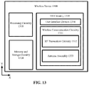
- FIG. 13 illustrates an example of a wireless device 1300 according to one embodiment.
- the wireless device 1300 may include any of the aforementioned antenna assemblies or their variations for transmitting and/or receiving wireless signals.
- the wireless device 1300 includes processing circuitry 1310 , which may further include one or more of: arithmetic and logic units (ALUs), control circuitry, cache memory, and/or other processing circuitry.
- ALUs arithmetic and logic units
- Non-limiting examples of the wireless device 1300 include smartphones, smartwatches, tablets, laptops, Internet-of-things (IoT) devices, navigation devices, multimedia devices, and other computing and/or communication devices having wireless communication capabilities.
- IoT Internet-of-things
- the wireless device 1300 further includes memory and storage circuitry 1320 coupled to the processing circuitry 1310 .
- the memory and storage circuitry 1320 may include memory devices such as dynamic random access memory (DRAM), static RAM (SRAM), flash memory and other volatile or non-volatile memory devices.
- the memory and storage circuitry 1320 may further include storage devices, for example, any type of solid-state, magnetic and/or optical storage device.
- the wireless device 1300 also includes input/output (I/O) circuitry 1330 which may further include user interface devices 1340 , such as one or more of: a display, a speaker, a microphone, a camera, touch sensors, buttons, a keyboard and/or a keypad, etc.
- the I/O circuitry 1330 further include wireless communication circuitry 1331 for communicating wirelessly with external systems.
- the wireless communication circuitry 1331 may include radio-frequency (RF) transceiver circuitry 1332 for handling various RF communication bands used in one or more of: WiFi, Bluetooth, cellular, Global Positioning System (GPS), millimeter wave, any short-range and/or long-range networks.
- RF radio-frequency
- the wireless communication circuitry 1331 includes an antenna assembly 1333 coupled to the RF transceiver circuitry 1332 .
- the antenna assembly 1333 may include the aforementioned antenna elements, antenna subarrays and/or their variations; e.g., the end-fire antenna elements and the end-fire antenna subarrays shown and/or described with reference to FIGS. 1-12 .
- the RF transceiver circuitry 1332 is disposed on a ground plane (not shown) which is parallel to the X-Y plane.
- the antenna assembly 1333 radiates in two or more frequency bands in the end-fire direction; i.e., in a direction parallel to the X-Y plane.
- the antenna assembly 1333 may additionally include broad-side antenna elements and/or antenna subarrays radiating in two or more frequency bands in a direction perpendicular to the X-Y plane.
Abstract
Description
Claims (10)
Priority Applications (3)
| Application Number | Priority Date | Filing Date | Title |
|---|---|---|---|
| US16/378,281 US11024981B2 (en) | 2018-04-13 | 2019-04-08 | Multi-band endfire antennas and arrays |
| TW108112619A TWI702757B (en) | 2018-04-13 | 2019-04-11 | Multi-band endfire antennas and arrays |
| CN201910292800.8A CN110380234B (en) | 2018-04-13 | 2019-04-12 | Multi-band endfire antenna and array |
Applications Claiming Priority (2)
| Application Number | Priority Date | Filing Date | Title |
|---|---|---|---|
| US201862657093P | 2018-04-13 | 2018-04-13 | |
| US16/378,281 US11024981B2 (en) | 2018-04-13 | 2019-04-08 | Multi-band endfire antennas and arrays |
Publications (2)
| Publication Number | Publication Date |
|---|---|
| US20190319369A1 US20190319369A1 (en) | 2019-10-17 |
| US11024981B2 true US11024981B2 (en) | 2021-06-01 |
Family
ID=68160510
Family Applications (1)
| Application Number | Title | Priority Date | Filing Date |
|---|---|---|---|
| US16/378,281 Active US11024981B2 (en) | 2018-04-13 | 2019-04-08 | Multi-band endfire antennas and arrays |
Country Status (3)
| Country | Link |
|---|---|
| US (1) | US11024981B2 (en) |
| CN (1) | CN110380234B (en) |
| TW (1) | TWI702757B (en) |
Families Citing this family (12)
| Publication number | Priority date | Publication date | Assignee | Title |
|---|---|---|---|---|
| US10263342B2 (en) | 2013-10-15 | 2019-04-16 | Northrop Grumman Systems Corporation | Reflectarray antenna system |
| US11075456B1 (en) | 2017-08-31 | 2021-07-27 | Northrop Grumman Systems Corporation | Printed board antenna system |
| US20190379130A1 (en) * | 2018-06-06 | 2019-12-12 | Mediatek Inc. | Antenna device used to perform dynamic control for feeding points and radio frequency chain circuit |
| KR102578033B1 (en) * | 2018-10-30 | 2023-09-13 | 엘지전자 주식회사 | Antenna system loaed in vehicle and vehicle comprising the same |
| US10944164B2 (en) * | 2019-03-13 | 2021-03-09 | Northrop Grumman Systems Corporation | Reflectarray antenna for transmission and reception at multiple frequency bands |
| CN111864407B (en) * | 2019-04-25 | 2021-08-27 | 大唐移动通信设备有限公司 | Quasi-yagi antenna array and millimeter wave base station equipment |
| KR102628013B1 (en) * | 2019-06-10 | 2024-01-22 | 삼성전자주식회사 | Wideband antenna and antenna module including the same |
| US11404786B2 (en) * | 2019-07-03 | 2022-08-02 | City University Of Hong Kong | Planar complementary antenna and related antenna array |
| US10892549B1 (en) | 2020-02-28 | 2021-01-12 | Northrop Grumman Systems Corporation | Phased-array antenna system |
| KR20210122956A (en) | 2020-04-01 | 2021-10-13 | 삼성전자주식회사 | Multi-band antenna device |
| KR102568208B1 (en) * | 2020-05-22 | 2023-08-21 | 엘지전자 주식회사 | Electronic device having an antenna |
| CN111786131B (en) * | 2020-08-10 | 2021-05-25 | 南通大学 | Broadband quasi-end-fire microstrip yagi antenna |
Citations (34)
| Publication number | Priority date | Publication date | Assignee | Title |
|---|---|---|---|---|
| DE1930660A1 (en) * | 1969-06-18 | 1971-01-14 | Kathrein Werke Kg | Asymmetrically fed dipole |
| US5485167A (en) | 1989-12-08 | 1996-01-16 | Hughes Aircraft Company | Multi-frequency band phased-array antenna using multiple layered dipole arrays |
| US6816124B2 (en) | 2001-11-07 | 2004-11-09 | Ems Technologies, Inc. | Linearly-polarized dual-band base-station antenna |
| US20090231225A1 (en) * | 2008-03-11 | 2009-09-17 | Debabani Choudhury | Wireless antenna array system architecture and methods to achieve 3D beam coverage |
| US20100167666A1 (en) * | 2008-12-31 | 2010-07-01 | Debabani Choudhury | Integrated Array Transmit/Receive Module |
| US20110287731A1 (en) * | 2009-02-02 | 2011-11-24 | Kazutoshi Hase | Antenna and reception apparatus provided with antenna |
| US20130147664A1 (en) * | 2011-12-12 | 2013-06-13 | Qualcomm Incorporated | Reconfigurable millimeter wave multibeam antenna array |
| US20130273858A1 (en) * | 2011-09-08 | 2013-10-17 | Ra'anan Sover | Overlapped and staggered antenna arrays |
| US20130293420A1 (en) * | 2012-05-07 | 2013-11-07 | Wilocity Ltd. | Techniques for maximizing the size of an antenna array per radio module |
| US20140253382A1 (en) * | 2012-05-07 | 2014-09-11 | Wilocity, Ltd. | Graded-ground design in a millimeter-wave radio module |
| US20140320344A1 (en) * | 2012-05-07 | 2014-10-30 | QUALCOMM ATHEROS Incorporated | Techniques for operating phased array antennas in millimeterwave radio modules |
| US20150070228A1 (en) * | 2013-09-11 | 2015-03-12 | International Business Machines Corporation | Antenna-in-package structures with broadside and end-fire radiations |
| US20150148098A1 (en) * | 2013-11-27 | 2015-05-28 | Broadcom Corporation | Integrated circuit with antenna arrays and methods for use therewith |
| US20160248169A1 (en) * | 2015-02-23 | 2016-08-25 | Qualcomm Incorporated | Antenna structures and configurations for millimeter wavelength wireless communications |
| US20170012359A1 (en) * | 2014-02-28 | 2017-01-12 | Samsung Electronics Co., Ltd. | Method and device for extending beam area in wireless communication system |
| US20170062908A1 (en) * | 2015-08-26 | 2017-03-02 | Qualcomm Incorporated | Antenna arrays for communications devices |
| US20170222325A1 (en) * | 2014-10-20 | 2017-08-03 | Murata Manufacturing Co., Ltd. | Antenna module |
| US20170222333A1 (en) * | 2014-10-20 | 2017-08-03 | Murata Manufacturing Co., Ltd. | Wireless communication module |
| US20180090827A1 (en) * | 2016-09-28 | 2018-03-29 | Toyota Motor Engineering & Manufacturing North America, Inc. | Volumetric scan automotive radar with end-fire antenna on partially laminated multi-layer pcb |
| US10084241B1 (en) * | 2018-02-23 | 2018-09-25 | Qualcomm Incorporated | Dual-polarization antenna system |
| US20180309186A1 (en) * | 2017-04-20 | 2018-10-25 | Speed Wireless Technology Inc. | Antenna array suitable for 5g mobile terminal devices |
| US20190006751A1 (en) * | 2017-06-28 | 2019-01-03 | Samsung Electronics Co., Ltd. | Antenna device and electronic device comprising antenna |
| US20190109386A1 (en) * | 2017-10-11 | 2019-04-11 | Wispry, Inc. | Wideband phased mobile antenna array devices, systems, and methods |
| US10333209B2 (en) * | 2016-07-19 | 2019-06-25 | Toyota Motor Engineering & Manufacturing North America, Inc. | Compact volume scan end-fire radar for vehicle applications |
| US20190207304A1 (en) * | 2017-12-28 | 2019-07-04 | Samsung Electro-Mechanics Co., Ltd. | Antenna apparatus and antenna module |
| US20190288377A1 (en) * | 2016-11-25 | 2019-09-19 | Sony Mobile Communications, Inc. | Vertical antenna patch in cavity region |
| US20190326677A1 (en) * | 2016-11-30 | 2019-10-24 | Kyocera Corporation | Antenna, module substrate, and module |
| US20190334233A1 (en) * | 2018-04-30 | 2019-10-31 | Samsung Electro-Mechanics Co., Ltd. | Antenna apparatus and antenna module |
| US20200067188A1 (en) * | 2018-08-21 | 2020-02-27 | Htc Corporation | Integrated antenna structure |
| US20200220268A1 (en) * | 2019-01-04 | 2020-07-09 | Samsung Electro-Mechanics., Ltd. | Antenna apparatus |
| US20200266523A1 (en) * | 2019-02-14 | 2020-08-20 | Samsung Electronics Co., Ltd. | Antenna module and electronic device including the same |
| US20200303839A1 (en) * | 2019-03-21 | 2020-09-24 | Samsung Electro-Mechanics Co., Ltd. | Antenna apparatus |
| US20200381835A1 (en) * | 2019-05-30 | 2020-12-03 | Cyntec Co., Ltd. | Antenna structure |
| US20200395677A1 (en) * | 2019-06-12 | 2020-12-17 | Samsung Electro-Mechanics Co., Ltd. | Antenna apparatus |
Family Cites Families (5)
| Publication number | Priority date | Publication date | Assignee | Title |
|---|---|---|---|---|
| US20050219126A1 (en) * | 2004-03-26 | 2005-10-06 | Automotive Systems Laboratory, Inc. | Multi-beam antenna |
| KR20140059552A (en) * | 2012-11-08 | 2014-05-16 | 삼성전자주식회사 | End fire antenna apparatus and electronic apparatus having the same |
| EP3020091A1 (en) * | 2013-07-08 | 2016-05-18 | Qualcomm Incorporated | Techniques for operating phased array antennas in millimeter-wave radio modules |
| CN205828671U (en) * | 2016-08-02 | 2016-12-21 | 潍坊歌尔电子有限公司 | Double frequency miniature antenna |
| CN106450782B (en) * | 2016-10-20 | 2019-07-12 | 加特兰微电子科技(上海)有限公司 | Radar component |
-
2019
- 2019-04-08 US US16/378,281 patent/US11024981B2/en active Active
- 2019-04-11 TW TW108112619A patent/TWI702757B/en active
- 2019-04-12 CN CN201910292800.8A patent/CN110380234B/en active Active
Patent Citations (38)
| Publication number | Priority date | Publication date | Assignee | Title |
|---|---|---|---|---|
| DE1930660A1 (en) * | 1969-06-18 | 1971-01-14 | Kathrein Werke Kg | Asymmetrically fed dipole |
| US5485167A (en) | 1989-12-08 | 1996-01-16 | Hughes Aircraft Company | Multi-frequency band phased-array antenna using multiple layered dipole arrays |
| US6816124B2 (en) | 2001-11-07 | 2004-11-09 | Ems Technologies, Inc. | Linearly-polarized dual-band base-station antenna |
| US20090231225A1 (en) * | 2008-03-11 | 2009-09-17 | Debabani Choudhury | Wireless antenna array system architecture and methods to achieve 3D beam coverage |
| US7830312B2 (en) * | 2008-03-11 | 2010-11-09 | Intel Corporation | Wireless antenna array system architecture and methods to achieve 3D beam coverage |
| US20100167666A1 (en) * | 2008-12-31 | 2010-07-01 | Debabani Choudhury | Integrated Array Transmit/Receive Module |
| US20110287731A1 (en) * | 2009-02-02 | 2011-11-24 | Kazutoshi Hase | Antenna and reception apparatus provided with antenna |
| US20130273858A1 (en) * | 2011-09-08 | 2013-10-17 | Ra'anan Sover | Overlapped and staggered antenna arrays |
| US20130147664A1 (en) * | 2011-12-12 | 2013-06-13 | Qualcomm Incorporated | Reconfigurable millimeter wave multibeam antenna array |
| US20130293420A1 (en) * | 2012-05-07 | 2013-11-07 | Wilocity Ltd. | Techniques for maximizing the size of an antenna array per radio module |
| US20140253382A1 (en) * | 2012-05-07 | 2014-09-11 | Wilocity, Ltd. | Graded-ground design in a millimeter-wave radio module |
| US20140320344A1 (en) * | 2012-05-07 | 2014-10-30 | QUALCOMM ATHEROS Incorporated | Techniques for operating phased array antennas in millimeterwave radio modules |
| US20150070228A1 (en) * | 2013-09-11 | 2015-03-12 | International Business Machines Corporation | Antenna-in-package structures with broadside and end-fire radiations |
| US9819098B2 (en) * | 2013-09-11 | 2017-11-14 | International Business Machines Corporation | Antenna-in-package structures with broadside and end-fire radiations |
| US20150148098A1 (en) * | 2013-11-27 | 2015-05-28 | Broadcom Corporation | Integrated circuit with antenna arrays and methods for use therewith |
| US20170012359A1 (en) * | 2014-02-28 | 2017-01-12 | Samsung Electronics Co., Ltd. | Method and device for extending beam area in wireless communication system |
| US20170222333A1 (en) * | 2014-10-20 | 2017-08-03 | Murata Manufacturing Co., Ltd. | Wireless communication module |
| US10153557B2 (en) * | 2014-10-20 | 2018-12-11 | Murata Manufacturing Co., Ltd. | Antenna module |
| US20170222325A1 (en) * | 2014-10-20 | 2017-08-03 | Murata Manufacturing Co., Ltd. | Antenna module |
| US20160248169A1 (en) * | 2015-02-23 | 2016-08-25 | Qualcomm Incorporated | Antenna structures and configurations for millimeter wavelength wireless communications |
| US20170062908A1 (en) * | 2015-08-26 | 2017-03-02 | Qualcomm Incorporated | Antenna arrays for communications devices |
| US10333209B2 (en) * | 2016-07-19 | 2019-06-25 | Toyota Motor Engineering & Manufacturing North America, Inc. | Compact volume scan end-fire radar for vehicle applications |
| US20180090827A1 (en) * | 2016-09-28 | 2018-03-29 | Toyota Motor Engineering & Manufacturing North America, Inc. | Volumetric scan automotive radar with end-fire antenna on partially laminated multi-layer pcb |
| US20190288377A1 (en) * | 2016-11-25 | 2019-09-19 | Sony Mobile Communications, Inc. | Vertical antenna patch in cavity region |
| US20190326677A1 (en) * | 2016-11-30 | 2019-10-24 | Kyocera Corporation | Antenna, module substrate, and module |
| US20180309186A1 (en) * | 2017-04-20 | 2018-10-25 | Speed Wireless Technology Inc. | Antenna array suitable for 5g mobile terminal devices |
| US20190006751A1 (en) * | 2017-06-28 | 2019-01-03 | Samsung Electronics Co., Ltd. | Antenna device and electronic device comprising antenna |
| US20190109386A1 (en) * | 2017-10-11 | 2019-04-11 | Wispry, Inc. | Wideband phased mobile antenna array devices, systems, and methods |
| US20190207304A1 (en) * | 2017-12-28 | 2019-07-04 | Samsung Electro-Mechanics Co., Ltd. | Antenna apparatus and antenna module |
| US10084241B1 (en) * | 2018-02-23 | 2018-09-25 | Qualcomm Incorporated | Dual-polarization antenna system |
| US20190334233A1 (en) * | 2018-04-30 | 2019-10-31 | Samsung Electro-Mechanics Co., Ltd. | Antenna apparatus and antenna module |
| US20200067188A1 (en) * | 2018-08-21 | 2020-02-27 | Htc Corporation | Integrated antenna structure |
| US10862211B2 (en) * | 2018-08-21 | 2020-12-08 | Htc Corporation | Integrated antenna structure |
| US20200220268A1 (en) * | 2019-01-04 | 2020-07-09 | Samsung Electro-Mechanics., Ltd. | Antenna apparatus |
| US20200266523A1 (en) * | 2019-02-14 | 2020-08-20 | Samsung Electronics Co., Ltd. | Antenna module and electronic device including the same |
| US20200303839A1 (en) * | 2019-03-21 | 2020-09-24 | Samsung Electro-Mechanics Co., Ltd. | Antenna apparatus |
| US20200381835A1 (en) * | 2019-05-30 | 2020-12-03 | Cyntec Co., Ltd. | Antenna structure |
| US20200395677A1 (en) * | 2019-06-12 | 2020-12-17 | Samsung Electro-Mechanics Co., Ltd. | Antenna apparatus |
Also Published As
| Publication number | Publication date |
|---|---|
| TW201944654A (en) | 2019-11-16 |
| US20190319369A1 (en) | 2019-10-17 |
| CN110380234A (en) | 2019-10-25 |
| TWI702757B (en) | 2020-08-21 |
| CN110380234B (en) | 2021-09-21 |
Similar Documents
| Publication | Publication Date | Title |
|---|---|---|
| US11024981B2 (en) | Multi-band endfire antennas and arrays | |
| US11245202B2 (en) | Millimeter wave array antenna and mobile terminal | |
| KR101766216B1 (en) | Array antenna using artificial magnetic conductor | |
| US10892561B2 (en) | Multi-band dual-polarization antenna arrays | |
| US7642970B2 (en) | Antenna device and wireless communication apparatus using same | |
| US6483463B2 (en) | Diversity antenna system including two planar inverted F antennas | |
| US8780002B2 (en) | Multiple-input multiple-output (MIMO) multi-band antennas with a conductive neutralization line for signal decoupling | |
| US20180269577A1 (en) | Multiband antenna and wireless communication device | |
| US7847736B2 (en) | Multi section meander antenna | |
| WO2019165915A1 (en) | Millimeter wave antenna array and mobile terminal | |
| US9577337B2 (en) | Dual-polarized antenna for mobile communication base station | |
| US20040233111A1 (en) | Multi frequency magnetic dipole antenna structures and method of reusing the volume of an antenna | |
| US20100007560A1 (en) | Direct feeding type patch antenna | |
| CN109478721B (en) | Antenna, device with one or more antennas and communication device | |
| US10522908B2 (en) | Antenna control method | |
| TW201635647A (en) | Reconfigurable multi-band multi-function antenna | |
| CN111987437A (en) | Broadband miniaturization super-surface antenna based on double-layer capacitive loading | |
| KR101992620B1 (en) | The Antenna with High Gain and Omni-Directional characteristics | |
| US20100231462A1 (en) | Multi-band serially connected antenna element for multi-band wireless communication devices | |
| US20230335894A1 (en) | Low profile device comprising layers of coupled resonance structures | |
| CN112952340A (en) | Antenna structure, circuit board with antenna structure and communication equipment | |
| JP2016140046A (en) | Dual-polarized antenna | |
| CN107369910B (en) | Microstrip antenna based on directional diagram diversity and corresponding antenna array | |
| US11949175B2 (en) | Millimeter wave antenna tuner | |
| WO2024012659A1 (en) | Cavity-slot antenna apparatus and wireless communication apparatus |
Legal Events
| Date | Code | Title | Description |
|---|---|---|---|
| AS | Assignment |
Owner name: MEDIATEK INC., TAIWAN Free format text: ASSIGNMENT OF ASSIGNORS INTEREST;ASSIGNORS:CHIANG, CHUNG-HSIN;KAO, YEH-CHUN;YEH, SHIH-HUANG;AND OTHERS;SIGNING DATES FROM 20190315 TO 20190402;REEL/FRAME:048823/0722 |
|
| FEPP | Fee payment procedure |
Free format text: ENTITY STATUS SET TO UNDISCOUNTED (ORIGINAL EVENT CODE: BIG.); ENTITY STATUS OF PATENT OWNER: LARGE ENTITY |
|
| STPP | Information on status: patent application and granting procedure in general |
Free format text: NON FINAL ACTION MAILED |
|
| STPP | Information on status: patent application and granting procedure in general |
Free format text: RESPONSE TO NON-FINAL OFFICE ACTION ENTERED AND FORWARDED TO EXAMINER |
|
| STPP | Information on status: patent application and granting procedure in general |
Free format text: RESPONSE TO NON-FINAL OFFICE ACTION ENTERED AND FORWARDED TO EXAMINER |
|
| STPP | Information on status: patent application and granting procedure in general |
Free format text: NOTICE OF ALLOWANCE MAILED -- APPLICATION RECEIVED IN OFFICE OF PUBLICATIONS |
|
| STPP | Information on status: patent application and granting procedure in general |
Free format text: AWAITING TC RESP., ISSUE FEE NOT PAID |
|
| STPP | Information on status: patent application and granting procedure in general |
Free format text: NOTICE OF ALLOWANCE MAILED -- APPLICATION RECEIVED IN OFFICE OF PUBLICATIONS |
|
| STPP | Information on status: patent application and granting procedure in general |
Free format text: PUBLICATIONS -- ISSUE FEE PAYMENT RECEIVED |
|
| STPP | Information on status: patent application and granting procedure in general |
Free format text: PUBLICATIONS -- ISSUE FEE PAYMENT VERIFIED |
|
| STCF | Information on status: patent grant |
Free format text: PATENTED CASE |