US10866751B2 - Method for managing flash memory module and associated flash memory controller - Google Patents
Method for managing flash memory module and associated flash memory controller Download PDFInfo
- Publication number
- US10866751B2 US10866751B2 US16/009,174 US201816009174A US10866751B2 US 10866751 B2 US10866751 B2 US 10866751B2 US 201816009174 A US201816009174 A US 201816009174A US 10866751 B2 US10866751 B2 US 10866751B2
- Authority
- US
- United States
- Prior art keywords
- page
- flash memory
- temporary
- temporary block
- pages
- Prior art date
- Legal status (The legal status is an assumption and is not a legal conclusion. Google has not performed a legal analysis and makes no representation as to the accuracy of the status listed.)
- Active
Links
- 238000000034 method Methods 0.000 title claims abstract description 25
- 238000013507 mapping Methods 0.000 claims description 30
- 238000011084 recovery Methods 0.000 claims description 7
- 230000004044 response Effects 0.000 claims 1
- 238000010586 diagram Methods 0.000 description 7
- 238000012986 modification Methods 0.000 description 3
- 230000004048 modification Effects 0.000 description 3
- 101100077211 Caenorhabditis elegans mlc-1 gene Proteins 0.000 description 1
- 230000004075 alteration Effects 0.000 description 1
- 238000013459 approach Methods 0.000 description 1
- 238000010420 art technique Methods 0.000 description 1
- 230000003139 buffering effect Effects 0.000 description 1
- 238000012937 correction Methods 0.000 description 1
- 238000013461 design Methods 0.000 description 1
- 239000007787 solid Substances 0.000 description 1
Images


Classifications
-
- G—PHYSICS
- G06—COMPUTING; CALCULATING OR COUNTING
- G06F—ELECTRIC DIGITAL DATA PROCESSING
- G06F12/00—Accessing, addressing or allocating within memory systems or architectures
- G06F12/02—Addressing or allocation; Relocation
- G06F12/0223—User address space allocation, e.g. contiguous or non contiguous base addressing
- G06F12/023—Free address space management
- G06F12/0238—Memory management in non-volatile memory, e.g. resistive RAM or ferroelectric memory
- G06F12/0246—Memory management in non-volatile memory, e.g. resistive RAM or ferroelectric memory in block erasable memory, e.g. flash memory
-
- G—PHYSICS
- G06—COMPUTING; CALCULATING OR COUNTING
- G06F—ELECTRIC DIGITAL DATA PROCESSING
- G06F11/00—Error detection; Error correction; Monitoring
- G06F11/07—Responding to the occurrence of a fault, e.g. fault tolerance
- G06F11/14—Error detection or correction of the data by redundancy in operation
- G06F11/1402—Saving, restoring, recovering or retrying
- G06F11/1415—Saving, restoring, recovering or retrying at system level
- G06F11/1441—Resetting or repowering
-
- G—PHYSICS
- G06—COMPUTING; CALCULATING OR COUNTING
- G06F—ELECTRIC DIGITAL DATA PROCESSING
- G06F11/00—Error detection; Error correction; Monitoring
- G06F11/07—Responding to the occurrence of a fault, e.g. fault tolerance
- G06F11/14—Error detection or correction of the data by redundancy in operation
- G06F11/1402—Saving, restoring, recovering or retrying
- G06F11/1446—Point-in-time backing up or restoration of persistent data
- G06F11/1458—Management of the backup or restore process
-
- G—PHYSICS
- G06—COMPUTING; CALCULATING OR COUNTING
- G06F—ELECTRIC DIGITAL DATA PROCESSING
- G06F12/00—Accessing, addressing or allocating within memory systems or architectures
- G06F12/02—Addressing or allocation; Relocation
- G06F12/0223—User address space allocation, e.g. contiguous or non contiguous base addressing
- G06F12/0292—User address space allocation, e.g. contiguous or non contiguous base addressing using tables or multilevel address translation means
-
- G—PHYSICS
- G06—COMPUTING; CALCULATING OR COUNTING
- G06F—ELECTRIC DIGITAL DATA PROCESSING
- G06F12/00—Accessing, addressing or allocating within memory systems or architectures
- G06F12/02—Addressing or allocation; Relocation
- G06F12/08—Addressing or allocation; Relocation in hierarchically structured memory systems, e.g. virtual memory systems
- G06F12/10—Address translation
- G06F12/1009—Address translation using page tables, e.g. page table structures
-
- G—PHYSICS
- G06—COMPUTING; CALCULATING OR COUNTING
- G06F—ELECTRIC DIGITAL DATA PROCESSING
- G06F3/00—Input arrangements for transferring data to be processed into a form capable of being handled by the computer; Output arrangements for transferring data from processing unit to output unit, e.g. interface arrangements
- G06F3/06—Digital input from, or digital output to, record carriers, e.g. RAID, emulated record carriers or networked record carriers
- G06F3/0601—Interfaces specially adapted for storage systems
- G06F3/0602—Interfaces specially adapted for storage systems specifically adapted to achieve a particular effect
- G06F3/0604—Improving or facilitating administration, e.g. storage management
-
- G—PHYSICS
- G06—COMPUTING; CALCULATING OR COUNTING
- G06F—ELECTRIC DIGITAL DATA PROCESSING
- G06F3/00—Input arrangements for transferring data to be processed into a form capable of being handled by the computer; Output arrangements for transferring data from processing unit to output unit, e.g. interface arrangements
- G06F3/06—Digital input from, or digital output to, record carriers, e.g. RAID, emulated record carriers or networked record carriers
- G06F3/0601—Interfaces specially adapted for storage systems
- G06F3/0602—Interfaces specially adapted for storage systems specifically adapted to achieve a particular effect
- G06F3/0614—Improving the reliability of storage systems
-
- G—PHYSICS
- G06—COMPUTING; CALCULATING OR COUNTING
- G06F—ELECTRIC DIGITAL DATA PROCESSING
- G06F3/00—Input arrangements for transferring data to be processed into a form capable of being handled by the computer; Output arrangements for transferring data from processing unit to output unit, e.g. interface arrangements
- G06F3/06—Digital input from, or digital output to, record carriers, e.g. RAID, emulated record carriers or networked record carriers
- G06F3/0601—Interfaces specially adapted for storage systems
- G06F3/0628—Interfaces specially adapted for storage systems making use of a particular technique
- G06F3/0638—Organizing or formatting or addressing of data
- G06F3/064—Management of blocks
-
- G—PHYSICS
- G06—COMPUTING; CALCULATING OR COUNTING
- G06F—ELECTRIC DIGITAL DATA PROCESSING
- G06F3/00—Input arrangements for transferring data to be processed into a form capable of being handled by the computer; Output arrangements for transferring data from processing unit to output unit, e.g. interface arrangements
- G06F3/06—Digital input from, or digital output to, record carriers, e.g. RAID, emulated record carriers or networked record carriers
- G06F3/0601—Interfaces specially adapted for storage systems
- G06F3/0628—Interfaces specially adapted for storage systems making use of a particular technique
- G06F3/0655—Vertical data movement, i.e. input-output transfer; data movement between one or more hosts and one or more storage devices
- G06F3/0656—Data buffering arrangements
-
- G—PHYSICS
- G06—COMPUTING; CALCULATING OR COUNTING
- G06F—ELECTRIC DIGITAL DATA PROCESSING
- G06F3/00—Input arrangements for transferring data to be processed into a form capable of being handled by the computer; Output arrangements for transferring data from processing unit to output unit, e.g. interface arrangements
- G06F3/06—Digital input from, or digital output to, record carriers, e.g. RAID, emulated record carriers or networked record carriers
- G06F3/0601—Interfaces specially adapted for storage systems
- G06F3/0668—Interfaces specially adapted for storage systems adopting a particular infrastructure
- G06F3/0671—In-line storage system
- G06F3/0673—Single storage device
- G06F3/0679—Non-volatile semiconductor memory device, e.g. flash memory, one time programmable memory [OTP]
-
- G—PHYSICS
- G06—COMPUTING; CALCULATING OR COUNTING
- G06F—ELECTRIC DIGITAL DATA PROCESSING
- G06F2212/00—Indexing scheme relating to accessing, addressing or allocation within memory systems or architectures
- G06F2212/72—Details relating to flash memory management
- G06F2212/7201—Logical to physical mapping or translation of blocks or pages
-
- G—PHYSICS
- G06—COMPUTING; CALCULATING OR COUNTING
- G06F—ELECTRIC DIGITAL DATA PROCESSING
- G06F2212/00—Indexing scheme relating to accessing, addressing or allocation within memory systems or architectures
- G06F2212/72—Details relating to flash memory management
- G06F2212/7203—Temporary buffering, e.g. using volatile buffer or dedicated buffer blocks
Definitions
- the present invention relates to a flash memory, and more particularly, to a method for managing a flash memory module, and an associated flash memory controller.
- the flash memory controller when the flash memory controller writes data into Multiple-Level Cell (MLC) blocks or Triple-Level Cell (TLC) blocks in the flash memory module, the data amount of a single writing is quite large, such as 64 KB or 128 KB.
- the flash memory controller When the flash memory controller writes random data of a small amount (e.g. 4 KB), the flash memory controller will have to add 60 KB or 124 KB dummy data into the 4 KB random data to ensure the data amount of a single writing is 64 KB or 128 KB.
- one approach sets an additional temporary block in the flash memory module to collect the random data, and then writes the temporary block back to said MLC or TLC blocks when enough data has been collected. If power off recovery (POR) or sudden power off recovery (SPOR) occurs during the data writing process, the creation time of data in the temporary blocks, MLC or TLC blocks cannot be determined, resulting in difficulties in creating an address mapping table later on.
- POR power off recovery
- SPOR sudden power off recovery
- an objective of the present invention is to provide a method for managing a flash memory module, which is capable of correctly determining the creation time of data in temporary blocks, MLC blocks or TLC blocks even when said POR or SPOR problem has occurred, so that the address mapping table can be recreated smoothly, thus solving the problem existing in the related arts.
- a method for managing a flash memory module comprises a plurality of flash memory chips, each comprising a plurality of first temporary blocks and a plurality of second temporary blocks. Each of the first and second temporary blocks comprises a plurality of pages.
- the method comprises: writing first data into a second temporary block of the second temporary blocks; and when access of the flash memory module meets a specific condition, moving the first data stored in the second temporary block to a first temporary block of the first temporary blocks, and recording current information of a first blank page of the second temporary block into the first temporary block.
- a method for managing a flash memory module comprises a plurality of flash memory chips, each comprising a plurality of first temporary blocks and a plurality of second temporary blocks. Each of the first temporary blocks and second temporary blocks comprises a plurality of pages.
- the method comprises: when a power off recovery (POR) state occurs, reading contents of a spare region of a page in a first temporary block, and determining a page serial number; determining pages in a second temporary block that are sorted prior to a page having the page serial number as invalid pages; and determining pages in the second temporary block that are sorted from the page having the page serial number as valid pages.
- POR power off recovery
- a flash memory controller is disclosed.
- the flash memory controller is used to access a flash memory module.
- the flash memory module comprises a plurality of flash memory chips, each comprising a plurality of first temporary blocks and a plurality of second temporary blocks. Each of the first temporary blocks and the second temporary blocks comprises a plurality of pages.
- the flash memory controller comprises a read-only memory (ROM) and a microprocessor.
- the ROM is arranged to store a code
- the microprocessor is arranged to execute the code in order to control access of the flash memory module, wherein the microprocessor writes first data into a second temporary block within the second temporary blocks; and when the access of the flash memory module meets a specific condition, the microprocessor moves the first data stored in the second temporary block to a first temporary block of the plurality of first temporary blocks, and records current information of a first blank page of the second temporary block into the first temporary block.
- a flash memory controller is disclosed, wherein the flash memory controller is arranged to access a flash memory module, the flash memory module comprises a plurality of flash memory chips each comprising a plurality of first temporary blocks and a plurality of second temporary blocks, wherein each of the first temporary blocks and the second temporary blocks comprises a plurality of pages, and the flash memory controller comprises a ROM, arranged to store a code, and a microprocessor arranged to execute the code in order to control access of the flash memory module.
- the microprocessor reads contents of a spare region of a page in a first temporary block, and determines a page serial number.
- the microprocessor determines pages in a second temporary block that is sorted prior to a page having the page serial number as invalid pages, and determines pages in the second temporary block sorted from the page having the page serial number as valid pages.
- FIG. 1 is a diagram illustrating a memory device according to an embodiment of the present invention.
- FIG. 2 is a flowchart illustrating a method of managing a flash memory module according to an embodiment of the present invention.
- FIG. 3A is a diagram illustrating the flash memory module shown in FIG. 1 .
- FIG. 3B is a diagram illustrating super blocks according to an embodiment of the present invention.
- FIG. 4 is a diagram illustrating the operation of writing data into temporary blocks and data blocks according to an embodiment of the present invention.
- FIG. 5 is a flowchart illustrating a method of managing a flash memory module according to another embodiment of the present invention.
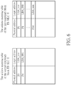
- FIG. 6 is a diagram illustrating recreating address mapping tables of temporary blocks and data blocks.
- FIG. 1 is a diagram illustrating a memory device 100 according to an embodiment of the present invention.
- the memory device 100 comprises a flash module 120 and a flash controller 110 , wherein the flash controller 110 is arranged to access the flash module 120 .
- the flash controller 110 comprises a microprocessor 112 , a read only memory (ROM) 112 M, a control logic 114 , a buffer memory 116 and an interface logic 118 .
- the ROM 112 M is arranged to store a code 112 C
- the microprocessor 112 is arranged to execute the code 112 C in order to control the access of the flash module 120 .
- the control logic 114 comprises an encoder 132 and a decoder 134 , wherein the encoder 132 is arranged to encode the data written into the flash module 120 to generate a corresponding check code (which can also be called an error correction code (ECC)), and the decoder 134 is arranged to decode the data read from the flash module 120 .
- ECC error correction code
- the flash module 120 comprises a plurality of flash chips each comprising a plurality of blocks, and the controller (e.g. the flash controller 110 that executes the code 112 C via the microprocessor 112 ) performs data erasing operations upon the flash module 120 using a “block” as the unit.
- a block may record a specific number of pages, wherein the controller (e.g. the flash controller 110 that executes the code 112 C via the microprocessor 112 ) performs data writing operations upon the flash module 120 using a “page” as the unit.
- the flash module 120 may be a 3D NAND-type flash.
- the flash controller 110 that executes the code 112 C via the microprocessor 112 may utilize its inner elements to perform various control operations, such as utilizing the control logic 114 to control access operations of the flash module 120 (especially the access operations of at least one block or at least one page), utilizing the buffer memory 116 to perform necessary buffering processes, and utilizing the interface logic 118 to communicate with a host device 130 .
- the memory device 100 may be a portable memory device (e.g. a memory card conforming to SD/MMC, CF, MS, XD specifications), and the host device 130 may be an electronic device connectable to memory devices, such as a cellphone, laptop computer, desktop computer, etc.
- the memory device 100 may be a solid state drive (SSD) or an embedded storage device that conforms to the Universal Flash Storage (UFS) or Embedded Multi Media Card (EMMC) specifications, in order to be configured in an electronic device (e.g. cellphone, laptop computer, desktop computer, etc.), wherein the host device 130 may be a processor of the electronic device.
- SSD solid state drive
- UFS Universal Flash Storage
- EMMC Embedded Multi Media Card
- Step 200 the flash memory controller 110 receives a writing command from the host device 130 , and accordingly writes data into a block of the flash memory module 120 .
- Step 202 the flash memory controller 110 receives a writing command from the host device 130 , and accordingly writes data into a block of the flash memory module 120 .
- the flash memory module 120 comprises the flash memory chips 310 , 320 each comprising a plurality of data blocks DB_ 0 -DB_M, a plurality of second temporary blocks TB_SLC_ 0 -TB_SLC_N and a plurality of first temporary blocks TB_MLC_ 0 -TB_MLC_K, wherein each block comprises a plurality of pages.
- the second temporary blocks TB_SLC_ 0 -TB_SLC_N are single-level cell (SLC) blocks
- the data block DB_ 0 -DB_M and the first temporary blocks TB_ MLC_ 0 -TB_MLC_K are MLC blocks, but the present invention is not limited thereto.
- the data blocks DB 0 -DB_M and/or the first temporary blocks TB_MLC_ 0 -TB_MLC_K may be triple-level cell (TLC) blocks.
- the second temporary blocks TB_SLC_ 0 -TB_SLC_N may also be formed by using MLC blocks instead of using SLC blocks.
- the writing mode of the flash memory module 120 can be “super block”-based as illustrated in FIG. 3B , which is a diagram illustrating super blocks according to an embodiment of the present invention. As shown in FIG. 3B , blocks of each of the flash memory chips 310 , 320 are divided into two planes.
- the flash memory module 120 merely comprises two flash memory chips 310 , 320 , four blocks located in different planes of the flash memory chips 310 , 320 may form a super block.
- the data blocks DB_ 0 , DB_ 1 in each of the flash memory chips 310 , 320 form a super block 352
- the second temporary blocks TB_SLC_ 0 , TB_SLC_ 1 in each of the flash memory chips 310 , 320 form a super block 354
- the first temporary blocks TB_MLC_ 0 , TB_MLC_ 1 in each of the flash memory chips 310 , 320 form a super block 356 , and so forth.
- each page in a super block (i.e. the four blocks) will be written.
- the flash memory controller 110 will have to write 64 KB data in total into a page of the super block 356 , which means sequentially writing the 64 KB data into a page of the first temporary block TB_MLC_ 0 in the flash memory chip 310 , a page of the first temporary block TB_MLC_ 1 in the flash memory chip 310 , a page of the first temporary block TB_MLC_ 0 in the flash memory chip 320 , and a page of the first temporary block TB_MLC_ 1 in the flash memory chip 320 .
- the flash memory controller 110 may write 128 KB data in total into two pages of the super block 356 , which means sequentially writing the 128 KB data into two pages of the first temporary block TB_MLC_ 0 in the flash memory chip 310 , two pages of the first temporary block TB_MLC_ 1 in the flash memory chip 310 , two pages of the first temporary block TB_ MLC_ 0 in the flash memory chip 320 , and two pages of the first temporary block TB_ MLC_ 1 in the flash memory chip 320 .
- the flash memory controller 110 when writing data into the flash memory module 120 , the flash memory controller 110 will select one of the first temporary blocks TB_MLC_ 0 -TB_MLC_K to store data. Since the data amount of the flash memory controller 110 writing to the first temporary blocks TB_MLC_ 0 -TB_MLC_K has to be higher than a threshold (e.g. 64 KB), in Step 204 , the flash memory controller 110 determines whether the access of the flash memory module 120 conforms to a specific condition; if not, the flow goes to Step 206 ; if yes, the flow goes to Step 208 .
- the specific condition may be whether the summation of the amount of written data based on the writing command mentioned in Step 202 and the data stored in the second temporary block that has not been moved to the first temporary block reaches the threshold or not.
- Step 206 the flash memory controller 110 writes the data corresponding to the writing command mentioned in Step 202 into the first temporary block.
- the flash memory controller 110 writes the data corresponding to the writing command mentioned in Step 202 along with the data stored in the second temporary block that has not been moved to the first temporary block into the first temporary block, and also records the current information of the first blank page of the second temporary block into the first temporary block. The flow then returns to Step 202 .
- FIG. 4 details the flow shown in FIG. 2 .
- the second temporary block TB_SLC_ 0 and the first temporary block TB_MLC_ 0 are illustrated in FIG. 4 , but one skilled in the art will readily realize that, in practice, said temporary block can be the super block shown in FIG. 3B .
- the flash memory controller 110 receives a first writing command from the host device 130 . Assuming that the data corresponding to the first writing command is random data (e.g. 4 KB) with a data amount lower than the threshold, the flash memory controller 110 will write the data corresponding to the first writing command into the first page P 0 in the second temporary block TB_SLC_ 0 .
- the flash memory controller 110 sequentially receives a second writing command and a third writing command from the host device 130 . Assuming that the data corresponding to the second and third writing commands is also random data (e.g. 4 KB), the flash memory controller 110 will sequentially write the data corresponding to the second or third writing commands into pages P 1 , P 2 of the second temporary block TB_SLC_ 0 . After that, the flash memory controller 110 receives the first to fourth writing commands from the host device 130 .
- the flash memory controller 110 will currently write valid data of the pages P 0 -P 2 of the second temporary block TB_SLC_ 0 (12 KB in total) along with the data corresponding to the fourth writing command (548 KB in total) to the pages P 0 -P 34 of the first temporary block TB_MLC_ 0 .
- the flash memory controller 110 will record the current information (i.e.
- the page P 3 of the first blank page of the second temporary block TB_SLC_ 0 into a spare region of each of the pages P 0 -P 34 .
- the size of the spare region is 64B or 128B, and the spare region is arranged to store managing information of the file system.
- the flash memory controller 110 before receiving data corresponding to the first, second and third writing commands, the flash memory controller 110 temporarily stores data corresponding to the first, second, or third writing command to the buffer 116 , and after writing the data corresponding to the first, second and third writing commands to the pages P 0 , P 1 and P 2 of the second temporary block TB_SLC_ 0 , the flash memory controller 110 deletes the corresponding data temporarily stored in the buffer 116 .
- the flash memory controller 110 writes the data corresponding to the first, second and third writing commands to the pages P 0 , P 1 and P 2 of the second temporary block TB_SLC_ 0 , the data corresponding to the first, second and third writing commands temporarily stored in the buffer 116 will not be deleted.
- the flash memory controller 110 When receiving the fourth writing command, the flash memory controller 110 will temporarily store data corresponding to the fourth writing command to the buffer 116 , and then directly reads the data corresponding to the first to fourth writing commands from the buffer 116 and writes the data altogether into the pages P 0 -P 34 of the first temporary block TB_MLC_ 0 . After that, the flash memory controller 110 deletes the data corresponding to the first to fourth writing commands temporarily stored in the buffer 116 . In another embodiment, after writing data corresponding to the first, second and third writing commands to the pages P 0 , P 1 and P 2 of the second temporary block TB_SLC_ 0 , the flash memory controller 110 will delete the data temporarily stored in the buffer 116 that correspond to the first, second and third writing commands.
- the flash memory controller 110 After the flash memory controller 110 receives the fourth writing command and temporarily stores the data corresponding to the fourth writing command to the buffer 116 , the flash memory controller 110 will read data from pages P 0 , P 1 and P 2 of the second temporary block TB_ SLC_ 0 , and then read the data corresponding to the first to fourth writing command from the buffer 116 and write the data altogether to the pages P 0 -P 34 of the first temporary block TB_ MLC_ 0 .
- the present invention is not limited thereto.
- the so-called “information of the first blank page of the second temporary block TB_SLC_ 0 ” can be any content related to the page P 3 and capable of determining the page P 3 .
- said information can be the serial number of the last written page of the second temporary block TB_SLC_ 0 . Similar modifications for the above design also fall within the scope of the present invention.
- the flash memory controller 110 receives a fifth writing command and a sixth writing command from the host device 130 .
- the flash memory controller 110 will sequentially write data corresponding to the fifth and sixth writing commands into the pages P 3 and P 4 of the second temporary block TB_SLC_ 0 .
- the data stored in the page P 4 of the second temporary block TB_SLC_ 0 is arranged to update the data stored in the page P 1 of the second temporary block TB_SLC_ 0 , i.e. the pages P 1 , P 4 of the second temporary block TB_SLC_ 0 and the page P 1 of the first temporary block TB_MLC_ 0 correspond to the same logic address.
- the purpose of recording information of the first blank page of the second temporary block TB_SLC_ 0 into the spare region of the data pages P 0 -P 34 the of the first temporary block TB_MLC_ 0 during the writing process is to prevent the power off recovery (POR) state or the sudden power off recovery (SPOR) state from happening, as the POR and SPOR states might make the data creation time of the first temporary block TB_MLC 0 and the second temporary block TB_SLC_ 0 unable to be determined, resulting in errors.
- POR power off recovery
- SPOR sudden power off recovery
- 5-6 will illustrate how to utilize the information of the first blank page of the second temporary block TB_SLC_ 0 recorded in the first temporary block TB_MLC_ 0 to correctly determine the creation time of data in the first temporary block TB_MLC_ 0 and the second temporary block TB_SLC_ 0 .
- Step 500 the memory device 100 encounters the POR or SPOR situation, and thereby loses the address mapping table stored in the buffer 116 .
- Step 502 the flash memory controller 110 reads the content of the spare region of the last written page of the first temporary block, in order to determine a page serial number for the second temporary block.
- Step 504 the flash memory controller 110 determines that the data sorted from the page serial number is new data, and the data sorted prior to the page serial number is old data (i.e. invalid data).
- Step 506 the flash memory controller 110 recreates the address mapping table according to the determination result of Step 504 .
- the flash memory controller 110 needs to recreate address mapping tables respectively corresponding to the second temporary block TB_SLC_ 0 and the first temporary block TB_MLC_ 0 . At this moment, the flash memory controller 110 will directly read content from the spare region of the last written page of the first temporary block TB_MLC_ 0 (i.e. P 34 ), and obtains a page serial number (i.e. P 3 ).
- the flash memory controller 110 will directly determine the data in the second temporary block TB_SLC_ 0 sorted from the page P 3 as new data, and the data sorted prior to the page P 3 as old data. In this way, the address mapping table of the second temporary block TB_SLC_ 0 only records physical addresses that relate to the pages P 3 , P 4 and corresponding logic addresses, without recording the address information related to the pages P 0 -P 2 .
- the flash memory controller 110 sequentially reads the information of each page in the first temporary block TB_MLC_ 0 , in order to recreate physical addresses and corresponding logic addresses of each of the pages P 0 -P 34 in the first temporary block TB_MLC_ 0 .
- the address mapping table of the second temporary block TB_SLC_ 0 recreated after the POR state or SPOR state only comprises the latest information
- the address mapping table of the second temporary block TB_SLC_ 0 and the address mapping table of the first temporary block TB_MLC_ 0 have the same logic address (e.g. the page P 4 of the second temporary block TB_SLC_ 0 shown in FIG. 6 and the page P 1 of the first temporary block TB_MLC_ 0 have the same logic address (LBA_ 001 ))
- LBA_ 001 logic address
- the data of page P 4 of the second temporary block TB_SLC_ 0 is arranged to update the page P 1 of the first temporary block TB_MLC_ 0 .
- the flash memory controller 110 if the flash memory controller 110 receives a reading command requesting reading the logic address LBA_ 001 , the flash memory controller 110 will directly obtain a corresponding physical address from the address mapping table of the second temporary block TB_SLC_ 0 , and then reads data from the page P 4 of the second temporary block TB_SLC_ 0 , without the need for reading content of the address mapping table of the first temporary block TB_MLC_ 0 .
- a garbage collection operation can be performed on the first temporary blocks in order to move the valid data therein to at least one data block (e.g. DB_ 0 ), and the first temporary blocks can be released afterwards for data writing.
- the method of the present invention for managing a flash memory module uses two temporary blocks (e.g. the first temporary block and the second temporary block) to store data written to the flash memory module, wherein the first temporary block is mainly arranged to store data with a data amount larger than a threshold (e.g. 64 KB), and the second temporary block is arranged to store random data with a data amount smaller than the threshold.
- a threshold e.g. 64 KB
- the data creation time of the second temporary block and first temporary block can be precisely determined after the occurrence of the POR or SPOR state, even when pages of the first temporary block and second temporary block have the same logic address, thus solving the problem existing in related art techniques.
Landscapes
- Engineering & Computer Science (AREA)
- Theoretical Computer Science (AREA)
- Physics & Mathematics (AREA)
- General Engineering & Computer Science (AREA)
- General Physics & Mathematics (AREA)
- Human Computer Interaction (AREA)
- Quality & Reliability (AREA)
- Techniques For Improving Reliability Of Storages (AREA)
- Read Only Memory (AREA)
Abstract
Description
Claims (10)
Priority Applications (1)
| Application Number | Priority Date | Filing Date | Title |
|---|---|---|---|
| US16/009,174 US10866751B2 (en) | 2017-06-25 | 2018-06-14 | Method for managing flash memory module and associated flash memory controller |
Applications Claiming Priority (5)
| Application Number | Priority Date | Filing Date | Title |
|---|---|---|---|
| US201762524602P | 2017-06-25 | 2017-06-25 | |
| TW107100021 | 2018-01-02 | ||
| TW107100021A TWI657339B (en) | 2017-06-25 | 2018-01-02 | Method for managing flash memory module and associated flash memory controller |
| TW107100021A | 2018-01-02 | ||
| US16/009,174 US10866751B2 (en) | 2017-06-25 | 2018-06-14 | Method for managing flash memory module and associated flash memory controller |
Publications (2)
| Publication Number | Publication Date |
|---|---|
| US20180373433A1 US20180373433A1 (en) | 2018-12-27 |
| US10866751B2 true US10866751B2 (en) | 2020-12-15 |
Family
ID=64693187
Family Applications (1)
| Application Number | Title | Priority Date | Filing Date |
|---|---|---|---|
| US16/009,174 Active US10866751B2 (en) | 2017-06-25 | 2018-06-14 | Method for managing flash memory module and associated flash memory controller |
Country Status (2)
| Country | Link |
|---|---|
| US (1) | US10866751B2 (en) |
| CN (1) | CN109117383B (en) |
Families Citing this family (7)
| Publication number | Priority date | Publication date | Assignee | Title |
|---|---|---|---|---|
| TWI734063B (en) * | 2019-01-02 | 2021-07-21 | 慧榮科技股份有限公司 | Flash memory controller, method for managing flash memory module and associated electronic device |
| TWI697778B (en) * | 2019-06-17 | 2020-07-01 | 慧榮科技股份有限公司 | A data storage device and a data processing method |
| TWI733360B (en) * | 2020-03-09 | 2021-07-11 | 慧榮科技股份有限公司 | Data storage device and data processing method |
| WO2021212337A1 (en) * | 2020-04-21 | 2021-10-28 | 华为技术有限公司 | Data access method and apparatus |
| US11494111B2 (en) * | 2020-12-17 | 2022-11-08 | Micron Technology, Inc. | Data operation based on valid memory unit count |
| CN113535085A (en) * | 2021-07-05 | 2021-10-22 | 歌尔科技有限公司 | Method, terminal device, system and storage medium for transmitting product identification |
| US11899977B2 (en) * | 2022-03-10 | 2024-02-13 | Silicon Motion, Inc. | Method and apparatus for performing access management of memory device with aid of serial number assignment timing control |
Citations (11)
| Publication number | Priority date | Publication date | Assignee | Title |
|---|---|---|---|---|
| US20090150597A1 (en) * | 2007-12-07 | 2009-06-11 | Phison Electronics Corp. | Data writing method for flash memory and controller using the same |
| US20090248965A1 (en) | 2008-03-25 | 2009-10-01 | Asmedia Technology Inc. | Hybrid flash memory device and method of controlling the same |
| TW200947455A (en) | 2008-05-06 | 2009-11-16 | Apacer Technology Inc | Method of managing storage unit and storage medium therefor |
| US20100287327A1 (en) * | 2009-05-06 | 2010-11-11 | Via Telecom, Inc. | Computing systems and methods for managing flash memory device |
| US20120110243A1 (en) * | 2010-10-29 | 2012-05-03 | Phison Electronics Corp. | Data writing method, memory controller, and memory storage apparatus |
| US20120284450A1 (en) * | 2011-05-06 | 2012-11-08 | Genesys Logic, Inc. | Flash memory system and managing and collecting methods for flash memory with invalid page messages thereof |
| TW201351417A (en) | 2012-06-04 | 2013-12-16 | Silicon Motion Inc | Flash memory apparatus and data accessing method for flash memory |
| TW201519251A (en) | 2013-11-05 | 2015-05-16 | Via Tech Inc | Non-volatile memory device and operation method thereof |
| US20160124845A1 (en) * | 2014-10-31 | 2016-05-05 | Silicon Motion, Inc. | Data Storage Device and Flash Memory Control Method |
| US20180356998A1 (en) * | 2017-06-07 | 2018-12-13 | ScaleFlux, Inc. | Solid-state storage power failure protection using distributed metadata checkpointing |
| US20190095132A1 (en) * | 2016-09-13 | 2019-03-28 | Hitachi, Ltd. | Computer system having data amount reduction function and storage control method |
Family Cites Families (2)
| Publication number | Priority date | Publication date | Assignee | Title |
|---|---|---|---|---|
| CN101814318B (en) * | 2009-02-25 | 2013-05-01 | 群联电子股份有限公司 | Multi level cell NAND flash storage system as well as controller and access method thereof |
| TWI417720B (en) * | 2009-05-06 | 2013-12-01 | Via Telecom Co Ltd | Flash memory managing methods and computing systems utilizing the same |
-
2018
- 2018-05-10 CN CN201810444354.3A patent/CN109117383B/en active Active
- 2018-06-14 US US16/009,174 patent/US10866751B2/en active Active
Patent Citations (11)
| Publication number | Priority date | Publication date | Assignee | Title |
|---|---|---|---|---|
| US20090150597A1 (en) * | 2007-12-07 | 2009-06-11 | Phison Electronics Corp. | Data writing method for flash memory and controller using the same |
| US20090248965A1 (en) | 2008-03-25 | 2009-10-01 | Asmedia Technology Inc. | Hybrid flash memory device and method of controlling the same |
| TW200947455A (en) | 2008-05-06 | 2009-11-16 | Apacer Technology Inc | Method of managing storage unit and storage medium therefor |
| US20100287327A1 (en) * | 2009-05-06 | 2010-11-11 | Via Telecom, Inc. | Computing systems and methods for managing flash memory device |
| US20120110243A1 (en) * | 2010-10-29 | 2012-05-03 | Phison Electronics Corp. | Data writing method, memory controller, and memory storage apparatus |
| US20120284450A1 (en) * | 2011-05-06 | 2012-11-08 | Genesys Logic, Inc. | Flash memory system and managing and collecting methods for flash memory with invalid page messages thereof |
| TW201351417A (en) | 2012-06-04 | 2013-12-16 | Silicon Motion Inc | Flash memory apparatus and data accessing method for flash memory |
| TW201519251A (en) | 2013-11-05 | 2015-05-16 | Via Tech Inc | Non-volatile memory device and operation method thereof |
| US20160124845A1 (en) * | 2014-10-31 | 2016-05-05 | Silicon Motion, Inc. | Data Storage Device and Flash Memory Control Method |
| US20190095132A1 (en) * | 2016-09-13 | 2019-03-28 | Hitachi, Ltd. | Computer system having data amount reduction function and storage control method |
| US20180356998A1 (en) * | 2017-06-07 | 2018-12-13 | ScaleFlux, Inc. | Solid-state storage power failure protection using distributed metadata checkpointing |
Also Published As
| Publication number | Publication date |
|---|---|
| CN109117383B (en) | 2022-09-20 |
| CN109117383A (en) | 2019-01-01 |
| US20180373433A1 (en) | 2018-12-27 |
Similar Documents
| Publication | Publication Date | Title |
|---|---|---|
| US10866751B2 (en) | Method for managing flash memory module and associated flash memory controller | |
| US10698809B2 (en) | Method, associated flash controller and electronic device for accessing flash module with data validity verification | |
| US10324789B2 (en) | Flash memory controller and memory device for accessing flash memory module, and associated method | |
| US9753649B2 (en) | Tracking intermix of writes and un-map commands across power cycles | |
| CN109977034B (en) | Data storage device and non-volatile memory operation method | |
| US10180805B2 (en) | Memory system and operating method thereof | |
| KR101491943B1 (en) | Transaction log recovery | |
| US10372619B2 (en) | Data backup method, data recovery method and storage controller | |
| CN109976938B (en) | Data storage device and non-volatile memory operation method | |
| KR20120060236A (en) | Power interrupt management | |
| US11733895B2 (en) | Control method of flash memory controller and associated flash memory controller and storage device | |
| US10606744B2 (en) | Method for accessing flash memory module and associated flash memory controller and electronic device | |
| CN110968522B (en) | Memory system, database system including the same, and method of operating the same | |
| US20190065361A1 (en) | Method for writing data into flash memory module and associated flash memory controller and electronic device | |
| US11809328B2 (en) | Control method of flash memory controller and associated flash memory controller and storage device | |
| CN110781023A (en) | Apparatus and method for processing data in memory system | |
| US11372578B2 (en) | Control method for flash memory controller and associated flash memory controller and memory device | |
| CN114121106A (en) | Memory system, memory controller and operating method thereof | |
| US11487475B2 (en) | Control method for referring to expired block table to perform expired block recycling operation and associated flash memory controller and memory device | |
| TWI693520B (en) | Method for performing system backup in a memory device, associated memory device and controller thereof, and associated electronic device | |
| US11210209B2 (en) | Method for managing flash memory module and associated flash memory controller and electronic device | |
| CN109753233B (en) | Memory system and operating method thereof | |
| US11662940B2 (en) | Data storage device and data processing method for restoring MLC/TLC memory to avoid degradation of access performance of a memory device caused by word line short | |
| CN110489053B (en) | Method for managing flash memory module, related flash memory controller and electronic device | |
| US11809748B2 (en) | Control method of flash memory controller and associated flash memory controller and electronic device |
Legal Events
| Date | Code | Title | Description |
|---|---|---|---|
| AS | Assignment |
Owner name: SILICON MOTION INC., TAIWAN Free format text: ASSIGNMENT OF ASSIGNORS INTEREST;ASSIGNOR:KE, KUAN-YU;REEL/FRAME:046095/0518 Effective date: 20180613 |
|
| FEPP | Fee payment procedure |
Free format text: ENTITY STATUS SET TO UNDISCOUNTED (ORIGINAL EVENT CODE: BIG.); ENTITY STATUS OF PATENT OWNER: LARGE ENTITY |
|
| STPP | Information on status: patent application and granting procedure in general |
Free format text: DOCKETED NEW CASE - READY FOR EXAMINATION |
|
| STPP | Information on status: patent application and granting procedure in general |
Free format text: NON FINAL ACTION MAILED |
|
| STPP | Information on status: patent application and granting procedure in general |
Free format text: RESPONSE TO NON-FINAL OFFICE ACTION ENTERED AND FORWARDED TO EXAMINER |
|
| STPP | Information on status: patent application and granting procedure in general |
Free format text: RESPONSE AFTER FINAL ACTION FORWARDED TO EXAMINER |
|
| STPP | Information on status: patent application and granting procedure in general |
Free format text: PUBLICATIONS -- ISSUE FEE PAYMENT RECEIVED |
|
| STCF | Information on status: patent grant |
Free format text: PATENTED CASE |
|
| MAFP | Maintenance fee payment |
Free format text: PAYMENT OF MAINTENANCE FEE, 4TH YEAR, LARGE ENTITY (ORIGINAL EVENT CODE: M1551); ENTITY STATUS OF PATENT OWNER: LARGE ENTITY Year of fee payment: 4 |