US10866516B2 - Metal-compound-removing solvent and method in lithography - Google Patents
Metal-compound-removing solvent and method in lithography Download PDFInfo
- Publication number
- US10866516B2 US10866516B2 US15/351,529 US201615351529A US10866516B2 US 10866516 B2 US10866516 B2 US 10866516B2 US 201615351529 A US201615351529 A US 201615351529A US 10866516 B2 US10866516 B2 US 10866516B2
- Authority
- US
- United States
- Prior art keywords
- wafer
- cleaning
- metal
- solvent
- photoresist
- Prior art date
- Legal status (The legal status is an assumption and is not a legal conclusion. Google has not performed a legal analysis and makes no representation as to the accuracy of the status listed.)
- Active, expires
Links
- 238000000034 method Methods 0.000 title claims abstract description 119
- 239000002904 solvent Substances 0.000 title claims abstract description 49
- 238000001459 lithography Methods 0.000 title claims description 37
- 239000000463 material Substances 0.000 claims abstract description 141
- 229910052751 metal Inorganic materials 0.000 claims abstract description 110
- 239000002184 metal Substances 0.000 claims abstract description 110
- 238000004140 cleaning Methods 0.000 claims abstract description 107
- 230000008569 process Effects 0.000 claims abstract description 86
- 229920002120 photoresistant polymer Polymers 0.000 claims abstract description 84
- 239000012530 fluid Substances 0.000 claims abstract description 66
- 239000002253 acid Substances 0.000 claims abstract description 40
- 238000001900 extreme ultraviolet lithography Methods 0.000 claims abstract description 33
- 238000010494 dissociation reaction Methods 0.000 claims abstract description 12
- 230000005593 dissociations Effects 0.000 claims abstract description 12
- 239000004065 semiconductor Substances 0.000 claims description 49
- 238000004519 manufacturing process Methods 0.000 claims description 34
- 238000010926 purge Methods 0.000 claims description 24
- 239000003960 organic solvent Substances 0.000 claims description 14
- 239000003125 aqueous solvent Substances 0.000 claims description 13
- 239000013522 chelant Substances 0.000 claims description 11
- 238000000576 coating method Methods 0.000 claims description 11
- 239000011248 coating agent Substances 0.000 claims description 8
- 239000004094 surface-active agent Substances 0.000 claims description 7
- 230000002209 hydrophobic effect Effects 0.000 claims description 3
- 150000007524 organic acids Chemical class 0.000 claims description 3
- 150000007530 organic bases Chemical class 0.000 claims description 3
- 238000009987 spinning Methods 0.000 claims description 3
- 239000004615 ingredient Substances 0.000 claims 1
- 239000002798 polar solvent Substances 0.000 claims 1
- TXEYQDLBPFQVAA-UHFFFAOYSA-N tetrafluoromethane Chemical compound FC(F)(F)F TXEYQDLBPFQVAA-UHFFFAOYSA-N 0.000 claims 1
- 235000012431 wafers Nutrition 0.000 description 141
- 239000000758 substrate Substances 0.000 description 38
- 239000000356 contaminant Substances 0.000 description 18
- -1 RuB Chemical class 0.000 description 13
- 210000001747 pupil Anatomy 0.000 description 13
- 238000010521 absorption reaction Methods 0.000 description 11
- 230000005855 radiation Effects 0.000 description 11
- VYPSYNLAJGMNEJ-UHFFFAOYSA-N Silicium dioxide Chemical compound O=[Si]=O VYPSYNLAJGMNEJ-UHFFFAOYSA-N 0.000 description 10
- 229910052710 silicon Inorganic materials 0.000 description 10
- 230000007246 mechanism Effects 0.000 description 9
- 229920000642 polymer Polymers 0.000 description 9
- XUIMIQQOPSSXEZ-UHFFFAOYSA-N Silicon Chemical compound [Si] XUIMIQQOPSSXEZ-UHFFFAOYSA-N 0.000 description 8
- 239000006096 absorbing agent Substances 0.000 description 8
- 239000010703 silicon Substances 0.000 description 8
- 230000008901 benefit Effects 0.000 description 7
- 238000011109 contamination Methods 0.000 description 7
- 230000003287 optical effect Effects 0.000 description 7
- 239000007921 spray Substances 0.000 description 7
- 238000005286 illumination Methods 0.000 description 6
- 238000000206 photolithography Methods 0.000 description 6
- 229910052581 Si3N4 Inorganic materials 0.000 description 5
- ATJFFYVFTNAWJD-UHFFFAOYSA-N Tin Chemical compound [Sn] ATJFFYVFTNAWJD-UHFFFAOYSA-N 0.000 description 5
- 238000005530 etching Methods 0.000 description 5
- 150000004767 nitrides Chemical class 0.000 description 5
- 238000000059 patterning Methods 0.000 description 5
- HQVNEWCFYHHQES-UHFFFAOYSA-N silicon nitride Chemical compound N12[Si]34N5[Si]62N3[Si]51N64 HQVNEWCFYHHQES-UHFFFAOYSA-N 0.000 description 5
- VKZRWSNIWNFCIQ-UHFFFAOYSA-N 2-[2-(1,2-dicarboxyethylamino)ethylamino]butanedioic acid Chemical compound OC(=O)CC(C(O)=O)NCCNC(C(O)=O)CC(O)=O VKZRWSNIWNFCIQ-UHFFFAOYSA-N 0.000 description 4
- KCXVZYZYPLLWCC-UHFFFAOYSA-N EDTA Chemical compound OC(=O)CN(CC(O)=O)CCN(CC(O)=O)CC(O)=O KCXVZYZYPLLWCC-UHFFFAOYSA-N 0.000 description 4
- QPCDCPDFJACHGM-UHFFFAOYSA-N N,N-bis{2-[bis(carboxymethyl)amino]ethyl}glycine Chemical compound OC(=O)CN(CC(O)=O)CCN(CC(=O)O)CCN(CC(O)=O)CC(O)=O QPCDCPDFJACHGM-UHFFFAOYSA-N 0.000 description 4
- GWEVSGVZZGPLCZ-UHFFFAOYSA-N Titan oxide Chemical compound O=[Ti]=O GWEVSGVZZGPLCZ-UHFFFAOYSA-N 0.000 description 4
- 239000011651 chromium Substances 0.000 description 4
- 229910052681 coesite Inorganic materials 0.000 description 4
- 229910052906 cristobalite Inorganic materials 0.000 description 4
- 238000009826 distribution Methods 0.000 description 4
- MRELNEQAGSRDBK-UHFFFAOYSA-N lanthanum(3+);oxygen(2-) Chemical compound [O-2].[O-2].[O-2].[La+3].[La+3] MRELNEQAGSRDBK-UHFFFAOYSA-N 0.000 description 4
- 229910044991 metal oxide Inorganic materials 0.000 description 4
- 150000004706 metal oxides Chemical class 0.000 description 4
- 239000000203 mixture Substances 0.000 description 4
- TWNQGVIAIRXVLR-UHFFFAOYSA-N oxo(oxoalumanyloxy)alumane Chemical compound O=[Al]O[Al]=O TWNQGVIAIRXVLR-UHFFFAOYSA-N 0.000 description 4
- 229960003330 pentetic acid Drugs 0.000 description 4
- 229910052707 ruthenium Inorganic materials 0.000 description 4
- 239000000377 silicon dioxide Substances 0.000 description 4
- 229910052682 stishovite Inorganic materials 0.000 description 4
- 229910052905 tridymite Inorganic materials 0.000 description 4
- QTBSBXVTEAMEQO-UHFFFAOYSA-N Acetic acid Chemical compound CC(O)=O QTBSBXVTEAMEQO-UHFFFAOYSA-N 0.000 description 3
- CSCPPACGZOOCGX-UHFFFAOYSA-N Acetone Chemical compound CC(C)=O CSCPPACGZOOCGX-UHFFFAOYSA-N 0.000 description 3
- WEVYAHXRMPXWCK-UHFFFAOYSA-N Acetonitrile Chemical compound CC#N WEVYAHXRMPXWCK-UHFFFAOYSA-N 0.000 description 3
- 239000004971 Cross linker Substances 0.000 description 3
- LFQSCWFLJHTTHZ-UHFFFAOYSA-N Ethanol Chemical compound CCO LFQSCWFLJHTTHZ-UHFFFAOYSA-N 0.000 description 3
- OKKJLVBELUTLKV-UHFFFAOYSA-N Methanol Chemical compound OC OKKJLVBELUTLKV-UHFFFAOYSA-N 0.000 description 3
- HEMHJVSKTPXQMS-UHFFFAOYSA-M Sodium hydroxide Chemical compound [OH-].[Na+] HEMHJVSKTPXQMS-UHFFFAOYSA-M 0.000 description 3
- 229910052782 aluminium Inorganic materials 0.000 description 3
- KRKNYBCHXYNGOX-UHFFFAOYSA-N citric acid Chemical compound OC(=O)CC(O)(C(O)=O)CC(O)=O KRKNYBCHXYNGOX-UHFFFAOYSA-N 0.000 description 3
- 150000001875 compounds Chemical class 0.000 description 3
- 238000013461 design Methods 0.000 description 3
- 239000003989 dielectric material Substances 0.000 description 3
- 229910052757 nitrogen Inorganic materials 0.000 description 3
- 230000036961 partial effect Effects 0.000 description 3
- 239000002245 particle Substances 0.000 description 3
- 238000002310 reflectometry Methods 0.000 description 3
- 229910052814 silicon oxide Inorganic materials 0.000 description 3
- 230000000007 visual effect Effects 0.000 description 3
- ARXJGSRGQADJSQ-UHFFFAOYSA-N 1-methoxypropan-2-ol Chemical compound COCC(C)O ARXJGSRGQADJSQ-UHFFFAOYSA-N 0.000 description 2
- IJGRMHOSHXDMSA-UHFFFAOYSA-N Atomic nitrogen Chemical compound N#N IJGRMHOSHXDMSA-UHFFFAOYSA-N 0.000 description 2
- VYZAMTAEIAYCRO-UHFFFAOYSA-N Chromium Chemical compound [Cr] VYZAMTAEIAYCRO-UHFFFAOYSA-N 0.000 description 2
- PIICEJLVQHRZGT-UHFFFAOYSA-N Ethylenediamine Chemical compound NCCN PIICEJLVQHRZGT-UHFFFAOYSA-N 0.000 description 2
- BDAGIHXWWSANSR-UHFFFAOYSA-N Formic acid Chemical compound OC=O BDAGIHXWWSANSR-UHFFFAOYSA-N 0.000 description 2
- AFVFQIVMOAPDHO-UHFFFAOYSA-N Methanesulfonic acid Chemical compound CS(O)(=O)=O AFVFQIVMOAPDHO-UHFFFAOYSA-N 0.000 description 2
- ZOKXTWBITQBERF-UHFFFAOYSA-N Molybdenum Chemical compound [Mo] ZOKXTWBITQBERF-UHFFFAOYSA-N 0.000 description 2
- ZMXDDKWLCZADIW-UHFFFAOYSA-N N,N-Dimethylformamide Chemical compound CN(C)C=O ZMXDDKWLCZADIW-UHFFFAOYSA-N 0.000 description 2
- LRHPLDYGYMQRHN-UHFFFAOYSA-N N-Butanol Chemical compound CCCCO LRHPLDYGYMQRHN-UHFFFAOYSA-N 0.000 description 2
- 229920000805 Polyaspartic acid Polymers 0.000 description 2
- KWYUFKZDYYNOTN-UHFFFAOYSA-M Potassium hydroxide Chemical compound [OH-].[K+] KWYUFKZDYYNOTN-UHFFFAOYSA-M 0.000 description 2
- KJTLSVCANCCWHF-UHFFFAOYSA-N Ruthenium Chemical compound [Ru] KJTLSVCANCCWHF-UHFFFAOYSA-N 0.000 description 2
- UCKMPCXJQFINFW-UHFFFAOYSA-N Sulphide Chemical compound [S-2] UCKMPCXJQFINFW-UHFFFAOYSA-N 0.000 description 2
- 239000000654 additive Substances 0.000 description 2
- 239000000956 alloy Substances 0.000 description 2
- 229910045601 alloy Inorganic materials 0.000 description 2
- CXOWYMLTGOFURZ-UHFFFAOYSA-N azanylidynechromium Chemical compound [Cr]#N CXOWYMLTGOFURZ-UHFFFAOYSA-N 0.000 description 2
- 229910052804 chromium Inorganic materials 0.000 description 2
- 239000002019 doping agent Substances 0.000 description 2
- 230000006870 function Effects 0.000 description 2
- 229910000449 hafnium oxide Inorganic materials 0.000 description 2
- WIHZLLGSGQNAGK-UHFFFAOYSA-N hafnium(4+);oxygen(2-) Chemical compound [O-2].[O-2].[Hf+4] WIHZLLGSGQNAGK-UHFFFAOYSA-N 0.000 description 2
- 229910052739 hydrogen Inorganic materials 0.000 description 2
- 239000001257 hydrogen Substances 0.000 description 2
- JVTAAEKCZFNVCJ-UHFFFAOYSA-N lactic acid Chemical compound CC(O)C(O)=O JVTAAEKCZFNVCJ-UHFFFAOYSA-N 0.000 description 2
- 230000000670 limiting effect Effects 0.000 description 2
- BJEPYKJPYRNKOW-UHFFFAOYSA-N malic acid Chemical compound OC(=O)C(O)CC(O)=O BJEPYKJPYRNKOW-UHFFFAOYSA-N 0.000 description 2
- 150000002736 metal compounds Chemical class 0.000 description 2
- 229910001092 metal group alloy Inorganic materials 0.000 description 2
- 229910052750 molybdenum Inorganic materials 0.000 description 2
- 239000011733 molybdenum Substances 0.000 description 2
- 239000011368 organic material Substances 0.000 description 2
- 108010064470 polyaspartate Proteins 0.000 description 2
- 238000012545 processing Methods 0.000 description 2
- 229910052705 radium Inorganic materials 0.000 description 2
- HCWPIIXVSYCSAN-UHFFFAOYSA-N radium atom Chemical compound [Ra] HCWPIIXVSYCSAN-UHFFFAOYSA-N 0.000 description 2
- 229920006395 saturated elastomer Polymers 0.000 description 2
- 150000003346 selenoethers Chemical class 0.000 description 2
- 229910021332 silicide Inorganic materials 0.000 description 2
- FVBUAEGBCNSCDD-UHFFFAOYSA-N silicide(4-) Chemical compound [Si-4] FVBUAEGBCNSCDD-UHFFFAOYSA-N 0.000 description 2
- 238000004528 spin coating Methods 0.000 description 2
- 229910052717 sulfur Inorganic materials 0.000 description 2
- WGTYBPLFGIVFAS-UHFFFAOYSA-M tetramethylammonium hydroxide Chemical compound [OH-].C[N+](C)(C)C WGTYBPLFGIVFAS-UHFFFAOYSA-M 0.000 description 2
- HXKKHQJGJAFBHI-UHFFFAOYSA-N 1-aminopropan-2-ol Chemical compound CC(O)CN HXKKHQJGJAFBHI-UHFFFAOYSA-N 0.000 description 1
- VSTXCZGEEVFJES-UHFFFAOYSA-N 1-cycloundecyl-1,5-diazacycloundec-5-ene Chemical compound C1CCCCCC(CCCC1)N1CCCCCC=NCCC1 VSTXCZGEEVFJES-UHFFFAOYSA-N 0.000 description 1
- HZAXFHJVJLSVMW-UHFFFAOYSA-N 2-Aminoethan-1-ol Chemical compound NCCO HZAXFHJVJLSVMW-UHFFFAOYSA-N 0.000 description 1
- 229940058020 2-amino-2-methyl-1-propanol Drugs 0.000 description 1
- KBIWNQVZKHSHTI-UHFFFAOYSA-N 4-n,4-n-dimethylbenzene-1,4-diamine;oxalic acid Chemical compound OC(=O)C(O)=O.CN(C)C1=CC=C(N)C=C1 KBIWNQVZKHSHTI-UHFFFAOYSA-N 0.000 description 1
- NSPMIYGKQJPBQR-UHFFFAOYSA-N 4H-1,2,4-triazole Chemical compound C=1N=CNN=1 NSPMIYGKQJPBQR-UHFFFAOYSA-N 0.000 description 1
- NIXOWILDQLNWCW-UHFFFAOYSA-M Acrylate Chemical compound [O-]C(=O)C=C NIXOWILDQLNWCW-UHFFFAOYSA-M 0.000 description 1
- QGZKDVFQNNGYKY-UHFFFAOYSA-N Ammonia Chemical compound N QGZKDVFQNNGYKY-UHFFFAOYSA-N 0.000 description 1
- 229910052582 BN Inorganic materials 0.000 description 1
- ZOXJGFHDIHLPTG-UHFFFAOYSA-N Boron Chemical compound [B] ZOXJGFHDIHLPTG-UHFFFAOYSA-N 0.000 description 1
- OKTJSMMVPCPJKN-UHFFFAOYSA-N Carbon Chemical group [C] OKTJSMMVPCPJKN-UHFFFAOYSA-N 0.000 description 1
- 229910052684 Cerium Inorganic materials 0.000 description 1
- RYGMFSIKBFXOCR-UHFFFAOYSA-N Copper Chemical compound [Cu] RYGMFSIKBFXOCR-UHFFFAOYSA-N 0.000 description 1
- VEXZGXHMUGYJMC-UHFFFAOYSA-N Hydrochloric acid Chemical compound Cl VEXZGXHMUGYJMC-UHFFFAOYSA-N 0.000 description 1
- UFHFLCQGNIYNRP-UHFFFAOYSA-N Hydrogen Chemical compound [H][H] UFHFLCQGNIYNRP-UHFFFAOYSA-N 0.000 description 1
- CPELXLSAUQHCOX-UHFFFAOYSA-N Hydrogen bromide Chemical compound Br CPELXLSAUQHCOX-UHFFFAOYSA-N 0.000 description 1
- GRYLNZFGIOXLOG-UHFFFAOYSA-N Nitric acid Chemical compound O[N+]([O-])=O GRYLNZFGIOXLOG-UHFFFAOYSA-N 0.000 description 1
- MUBZPKHOEPUJKR-UHFFFAOYSA-N Oxalic acid Natural products OC(=O)C(O)=O MUBZPKHOEPUJKR-UHFFFAOYSA-N 0.000 description 1
- NBIIXXVUZAFLBC-UHFFFAOYSA-N Phosphoric acid Chemical compound OP(O)(O)=O NBIIXXVUZAFLBC-UHFFFAOYSA-N 0.000 description 1
- 230000010748 Photoabsorption Effects 0.000 description 1
- 239000004793 Polystyrene Substances 0.000 description 1
- OFOBLEOULBTSOW-UHFFFAOYSA-N Propanedioic acid Natural products OC(=O)CC(O)=O OFOBLEOULBTSOW-UHFFFAOYSA-N 0.000 description 1
- 229910019895 RuSi Inorganic materials 0.000 description 1
- BQCADISMDOOEFD-UHFFFAOYSA-N Silver Chemical compound [Ag] BQCADISMDOOEFD-UHFFFAOYSA-N 0.000 description 1
- QAOWNCQODCNURD-UHFFFAOYSA-N Sulfuric acid Chemical compound OS(O)(=O)=O QAOWNCQODCNURD-UHFFFAOYSA-N 0.000 description 1
- WGLPBDUCMAPZCE-UHFFFAOYSA-N Trioxochromium Chemical compound O=[Cr](=O)=O WGLPBDUCMAPZCE-UHFFFAOYSA-N 0.000 description 1
- LEHOTFFKMJEONL-UHFFFAOYSA-N Uric Acid Chemical compound N1C(=O)NC(=O)C2=C1NC(=O)N2 LEHOTFFKMJEONL-UHFFFAOYSA-N 0.000 description 1
- TVWHNULVHGKJHS-UHFFFAOYSA-N Uric acid Natural products N1C(=O)NC(=O)C2NC(=O)NC21 TVWHNULVHGKJHS-UHFFFAOYSA-N 0.000 description 1
- HCHKCACWOHOZIP-UHFFFAOYSA-N Zinc Chemical compound [Zn] HCHKCACWOHOZIP-UHFFFAOYSA-N 0.000 description 1
- SLYSCVGKSGZCPI-UHFFFAOYSA-N [B]=O.[Ta] Chemical compound [B]=O.[Ta] SLYSCVGKSGZCPI-UHFFFAOYSA-N 0.000 description 1
- 229910052767 actinium Inorganic materials 0.000 description 1
- QQINRWTZWGJFDB-UHFFFAOYSA-N actinium atom Chemical compound [Ac] QQINRWTZWGJFDB-UHFFFAOYSA-N 0.000 description 1
- 230000000996 additive effect Effects 0.000 description 1
- 230000004075 alteration Effects 0.000 description 1
- XAGFODPZIPBFFR-UHFFFAOYSA-N aluminium Chemical compound [Al] XAGFODPZIPBFFR-UHFFFAOYSA-N 0.000 description 1
- CBTVGIZVANVGBH-UHFFFAOYSA-N aminomethyl propanol Chemical compound CC(C)(N)CO CBTVGIZVANVGBH-UHFFFAOYSA-N 0.000 description 1
- 239000011260 aqueous acid Substances 0.000 description 1
- 229910052785 arsenic Inorganic materials 0.000 description 1
- RQNWIZPPADIBDY-UHFFFAOYSA-N arsenic atom Chemical compound [As] RQNWIZPPADIBDY-UHFFFAOYSA-N 0.000 description 1
- 230000002238 attenuated effect Effects 0.000 description 1
- 229910052788 barium Inorganic materials 0.000 description 1
- DSAJWYNOEDNPEQ-UHFFFAOYSA-N barium atom Chemical compound [Ba] DSAJWYNOEDNPEQ-UHFFFAOYSA-N 0.000 description 1
- 239000002585 base Substances 0.000 description 1
- SRSXLGNVWSONIS-UHFFFAOYSA-N benzenesulfonic acid Chemical compound OS(=O)(=O)C1=CC=CC=C1 SRSXLGNVWSONIS-UHFFFAOYSA-N 0.000 description 1
- 229940092714 benzenesulfonic acid Drugs 0.000 description 1
- QRUDEWIWKLJBPS-UHFFFAOYSA-N benzotriazole Chemical compound C1=CC=C2N[N][N]C2=C1 QRUDEWIWKLJBPS-UHFFFAOYSA-N 0.000 description 1
- 229910052790 beryllium Inorganic materials 0.000 description 1
- 230000015572 biosynthetic process Effects 0.000 description 1
- XTDAIYZKROTZLD-UHFFFAOYSA-N boranylidynetantalum Chemical compound [Ta]#B XTDAIYZKROTZLD-UHFFFAOYSA-N 0.000 description 1
- 229910052796 boron Inorganic materials 0.000 description 1
- 229910052792 caesium Inorganic materials 0.000 description 1
- TVFDJXOCXUVLDH-UHFFFAOYSA-N caesium atom Chemical compound [Cs] TVFDJXOCXUVLDH-UHFFFAOYSA-N 0.000 description 1
- 239000003990 capacitor Substances 0.000 description 1
- 125000003178 carboxy group Chemical group [H]OC(*)=O 0.000 description 1
- GWXLDORMOJMVQZ-UHFFFAOYSA-N cerium Chemical compound [Ce] GWXLDORMOJMVQZ-UHFFFAOYSA-N 0.000 description 1
- 238000006243 chemical reaction Methods 0.000 description 1
- 229910000423 chromium oxide Inorganic materials 0.000 description 1
- 235000015165 citric acid Nutrition 0.000 description 1
- 230000000295 complement effect Effects 0.000 description 1
- 230000001010 compromised effect Effects 0.000 description 1
- 238000010276 construction Methods 0.000 description 1
- 238000007796 conventional method Methods 0.000 description 1
- 229910052802 copper Inorganic materials 0.000 description 1
- 239000010949 copper Substances 0.000 description 1
- 125000004122 cyclic group Chemical group 0.000 description 1
- 238000000354 decomposition reaction Methods 0.000 description 1
- 230000003247 decreasing effect Effects 0.000 description 1
- 238000011161 development Methods 0.000 description 1
- 230000018109 developmental process Effects 0.000 description 1
- 238000010586 diagram Methods 0.000 description 1
- 229910003460 diamond Inorganic materials 0.000 description 1
- 239000010432 diamond Substances 0.000 description 1
- 239000006185 dispersion Substances 0.000 description 1
- 238000005516 engineering process Methods 0.000 description 1
- CCIVGXIOQKPBKL-UHFFFAOYSA-M ethanesulfonate Chemical compound CCS([O-])(=O)=O CCIVGXIOQKPBKL-UHFFFAOYSA-M 0.000 description 1
- 230000005669 field effect Effects 0.000 description 1
- 235000019253 formic acid Nutrition 0.000 description 1
- 239000005350 fused silica glass Substances 0.000 description 1
- 239000007789 gas Substances 0.000 description 1
- 229910052732 germanium Inorganic materials 0.000 description 1
- GNPVGFCGXDBREM-UHFFFAOYSA-N germanium atom Chemical compound [Ge] GNPVGFCGXDBREM-UHFFFAOYSA-N 0.000 description 1
- 125000005843 halogen group Chemical group 0.000 description 1
- 238000010438 heat treatment Methods 0.000 description 1
- BHEPBYXIRTUNPN-UHFFFAOYSA-N hydridophosphorus(.) (triplet) Chemical compound [PH] BHEPBYXIRTUNPN-UHFFFAOYSA-N 0.000 description 1
- 238000003384 imaging method Methods 0.000 description 1
- 229910052738 indium Inorganic materials 0.000 description 1
- APFVFJFRJDLVQX-UHFFFAOYSA-N indium atom Chemical compound [In] APFVFJFRJDLVQX-UHFFFAOYSA-N 0.000 description 1
- 239000012212 insulator Substances 0.000 description 1
- 230000003993 interaction Effects 0.000 description 1
- 235000014655 lactic acid Nutrition 0.000 description 1
- 229910052746 lanthanum Inorganic materials 0.000 description 1
- FZLIPJUXYLNCLC-UHFFFAOYSA-N lanthanum atom Chemical compound [La] FZLIPJUXYLNCLC-UHFFFAOYSA-N 0.000 description 1
- VZCYOOQTPOCHFL-UPHRSURJSA-N maleic acid Chemical compound OC(=O)\C=C/C(O)=O VZCYOOQTPOCHFL-UPHRSURJSA-N 0.000 description 1
- 239000011976 maleic acid Substances 0.000 description 1
- 239000001630 malic acid Substances 0.000 description 1
- 235000011090 malic acid Nutrition 0.000 description 1
- 229940098779 methanesulfonic acid Drugs 0.000 description 1
- 238000004377 microelectronic Methods 0.000 description 1
- GALOTNBSUVEISR-UHFFFAOYSA-N molybdenum;silicon Chemical compound [Mo]#[Si] GALOTNBSUVEISR-UHFFFAOYSA-N 0.000 description 1
- 239000000178 monomer Substances 0.000 description 1
- 229910017604 nitric acid Inorganic materials 0.000 description 1
- NJPPVKZQTLUDBO-UHFFFAOYSA-N novaluron Chemical compound C1=C(Cl)C(OC(F)(F)C(OC(F)(F)F)F)=CC=C1NC(=O)NC(=O)C1=C(F)C=CC=C1F NJPPVKZQTLUDBO-UHFFFAOYSA-N 0.000 description 1
- GEVPUGOOGXGPIO-UHFFFAOYSA-N oxalic acid;dihydrate Chemical compound O.O.OC(=O)C(O)=O GEVPUGOOGXGPIO-UHFFFAOYSA-N 0.000 description 1
- 230000003647 oxidation Effects 0.000 description 1
- 238000007254 oxidation reaction Methods 0.000 description 1
- 230000010363 phase shift Effects 0.000 description 1
- 229920002223 polystyrene Polymers 0.000 description 1
- BDERNNFJNOPAEC-UHFFFAOYSA-N propan-1-ol Chemical compound CCCO BDERNNFJNOPAEC-UHFFFAOYSA-N 0.000 description 1
- 230000002829 reductive effect Effects 0.000 description 1
- 229910052709 silver Inorganic materials 0.000 description 1
- 239000004332 silver Substances 0.000 description 1
- 238000006467 substitution reaction Methods 0.000 description 1
- 229910052714 tellurium Inorganic materials 0.000 description 1
- PORWMNRCUJJQNO-UHFFFAOYSA-N tellurium atom Chemical compound [Te] PORWMNRCUJJQNO-UHFFFAOYSA-N 0.000 description 1
- VZCYOOQTPOCHFL-UHFFFAOYSA-N trans-butenedioic acid Natural products OC(=O)C=CC(O)=O VZCYOOQTPOCHFL-UHFFFAOYSA-N 0.000 description 1
- 238000012546 transfer Methods 0.000 description 1
- YNJBWRMUSHSURL-UHFFFAOYSA-N trichloroacetic acid Chemical compound OC(=O)C(Cl)(Cl)Cl YNJBWRMUSHSURL-UHFFFAOYSA-N 0.000 description 1
- ZMANZCXQSJIPKH-UHFFFAOYSA-O triethylammonium ion Chemical compound CC[NH+](CC)CC ZMANZCXQSJIPKH-UHFFFAOYSA-O 0.000 description 1
- ITMCEJHCFYSIIV-UHFFFAOYSA-N triflic acid Chemical compound OS(=O)(=O)C(F)(F)F ITMCEJHCFYSIIV-UHFFFAOYSA-N 0.000 description 1
- 229940116269 uric acid Drugs 0.000 description 1
- 238000005406 washing Methods 0.000 description 1
- XLYOFNOQVPJJNP-UHFFFAOYSA-N water Substances O XLYOFNOQVPJJNP-UHFFFAOYSA-N 0.000 description 1
- 229910052725 zinc Inorganic materials 0.000 description 1
- 239000011701 zinc Substances 0.000 description 1
Images


Classifications
-
- G—PHYSICS
- G03—PHOTOGRAPHY; CINEMATOGRAPHY; ANALOGOUS TECHNIQUES USING WAVES OTHER THAN OPTICAL WAVES; ELECTROGRAPHY; HOLOGRAPHY
- G03F—PHOTOMECHANICAL PRODUCTION OF TEXTURED OR PATTERNED SURFACES, e.g. FOR PRINTING, FOR PROCESSING OF SEMICONDUCTOR DEVICES; MATERIALS THEREFOR; ORIGINALS THEREFOR; APPARATUS SPECIALLY ADAPTED THEREFOR
- G03F7/00—Photomechanical, e.g. photolithographic, production of textured or patterned surfaces, e.g. printing surfaces; Materials therefor, e.g. comprising photoresists; Apparatus specially adapted therefor
- G03F7/26—Processing photosensitive materials; Apparatus therefor
-
- C—CHEMISTRY; METALLURGY
- C11—ANIMAL OR VEGETABLE OILS, FATS, FATTY SUBSTANCES OR WAXES; FATTY ACIDS THEREFROM; DETERGENTS; CANDLES
- C11D—DETERGENT COMPOSITIONS; USE OF SINGLE SUBSTANCES AS DETERGENTS; SOAP OR SOAP-MAKING; RESIN SOAPS; RECOVERY OF GLYCEROL
- C11D3/00—Other compounding ingredients of detergent compositions covered in group C11D1/00
- C11D3/43—Solvents
-
- G—PHYSICS
- G03—PHOTOGRAPHY; CINEMATOGRAPHY; ANALOGOUS TECHNIQUES USING WAVES OTHER THAN OPTICAL WAVES; ELECTROGRAPHY; HOLOGRAPHY
- G03F—PHOTOMECHANICAL PRODUCTION OF TEXTURED OR PATTERNED SURFACES, e.g. FOR PRINTING, FOR PROCESSING OF SEMICONDUCTOR DEVICES; MATERIALS THEREFOR; ORIGINALS THEREFOR; APPARATUS SPECIALLY ADAPTED THEREFOR
- G03F7/00—Photomechanical, e.g. photolithographic, production of textured or patterned surfaces, e.g. printing surfaces; Materials therefor, e.g. comprising photoresists; Apparatus specially adapted therefor
- G03F7/004—Photosensitive materials
- G03F7/0042—Photosensitive materials with inorganic or organometallic light-sensitive compounds not otherwise provided for, e.g. inorganic resists
- G03F7/0043—Chalcogenides; Silicon, germanium, arsenic or derivatives thereof; Metals, oxides or alloys thereof
-
- G—PHYSICS
- G03—PHOTOGRAPHY; CINEMATOGRAPHY; ANALOGOUS TECHNIQUES USING WAVES OTHER THAN OPTICAL WAVES; ELECTROGRAPHY; HOLOGRAPHY
- G03F—PHOTOMECHANICAL PRODUCTION OF TEXTURED OR PATTERNED SURFACES, e.g. FOR PRINTING, FOR PROCESSING OF SEMICONDUCTOR DEVICES; MATERIALS THEREFOR; ORIGINALS THEREFOR; APPARATUS SPECIALLY ADAPTED THEREFOR
- G03F7/00—Photomechanical, e.g. photolithographic, production of textured or patterned surfaces, e.g. printing surfaces; Materials therefor, e.g. comprising photoresists; Apparatus specially adapted therefor
- G03F7/16—Coating processes; Apparatus therefor
- G03F7/162—Coating on a rotating support, e.g. using a whirler or a spinner
-
- G—PHYSICS
- G03—PHOTOGRAPHY; CINEMATOGRAPHY; ANALOGOUS TECHNIQUES USING WAVES OTHER THAN OPTICAL WAVES; ELECTROGRAPHY; HOLOGRAPHY
- G03F—PHOTOMECHANICAL PRODUCTION OF TEXTURED OR PATTERNED SURFACES, e.g. FOR PRINTING, FOR PROCESSING OF SEMICONDUCTOR DEVICES; MATERIALS THEREFOR; ORIGINALS THEREFOR; APPARATUS SPECIALLY ADAPTED THEREFOR
- G03F7/00—Photomechanical, e.g. photolithographic, production of textured or patterned surfaces, e.g. printing surfaces; Materials therefor, e.g. comprising photoresists; Apparatus specially adapted therefor
- G03F7/16—Coating processes; Apparatus therefor
- G03F7/168—Finishing the coated layer, e.g. drying, baking, soaking
-
- G—PHYSICS
- G03—PHOTOGRAPHY; CINEMATOGRAPHY; ANALOGOUS TECHNIQUES USING WAVES OTHER THAN OPTICAL WAVES; ELECTROGRAPHY; HOLOGRAPHY
- G03F—PHOTOMECHANICAL PRODUCTION OF TEXTURED OR PATTERNED SURFACES, e.g. FOR PRINTING, FOR PROCESSING OF SEMICONDUCTOR DEVICES; MATERIALS THEREFOR; ORIGINALS THEREFOR; APPARATUS SPECIALLY ADAPTED THEREFOR
- G03F7/00—Photomechanical, e.g. photolithographic, production of textured or patterned surfaces, e.g. printing surfaces; Materials therefor, e.g. comprising photoresists; Apparatus specially adapted therefor
- G03F7/26—Processing photosensitive materials; Apparatus therefor
- G03F7/30—Imagewise removal using liquid means
- G03F7/3042—Imagewise removal using liquid means from printing plates transported horizontally through the processing stations
- G03F7/3057—Imagewise removal using liquid means from printing plates transported horizontally through the processing stations characterised by the processing units other than the developing unit, e.g. washing units
-
- G—PHYSICS
- G03—PHOTOGRAPHY; CINEMATOGRAPHY; ANALOGOUS TECHNIQUES USING WAVES OTHER THAN OPTICAL WAVES; ELECTROGRAPHY; HOLOGRAPHY
- G03F—PHOTOMECHANICAL PRODUCTION OF TEXTURED OR PATTERNED SURFACES, e.g. FOR PRINTING, FOR PROCESSING OF SEMICONDUCTOR DEVICES; MATERIALS THEREFOR; ORIGINALS THEREFOR; APPARATUS SPECIALLY ADAPTED THEREFOR
- G03F7/00—Photomechanical, e.g. photolithographic, production of textured or patterned surfaces, e.g. printing surfaces; Materials therefor, e.g. comprising photoresists; Apparatus specially adapted therefor
- G03F7/26—Processing photosensitive materials; Apparatus therefor
- G03F7/38—Treatment before imagewise removal, e.g. prebaking
-
- H—ELECTRICITY
- H01—ELECTRIC ELEMENTS
- H01L—SEMICONDUCTOR DEVICES NOT COVERED BY CLASS H10
- H01L21/00—Processes or apparatus adapted for the manufacture or treatment of semiconductor or solid state devices or of parts thereof
- H01L21/02—Manufacture or treatment of semiconductor devices or of parts thereof
- H01L21/02041—Cleaning
- H01L21/02057—Cleaning during device manufacture
- H01L21/0206—Cleaning during device manufacture during, before or after processing of insulating layers
-
- H—ELECTRICITY
- H01—ELECTRIC ELEMENTS
- H01L—SEMICONDUCTOR DEVICES NOT COVERED BY CLASS H10
- H01L21/00—Processes or apparatus adapted for the manufacture or treatment of semiconductor or solid state devices or of parts thereof
- H01L21/02—Manufacture or treatment of semiconductor devices or of parts thereof
- H01L21/02041—Cleaning
- H01L21/02082—Cleaning product to be cleaned
- H01L21/02087—Cleaning of wafer edges
-
- H—ELECTRICITY
- H01—ELECTRIC ELEMENTS
- H01L—SEMICONDUCTOR DEVICES NOT COVERED BY CLASS H10
- H01L21/00—Processes or apparatus adapted for the manufacture or treatment of semiconductor or solid state devices or of parts thereof
- H01L21/02—Manufacture or treatment of semiconductor devices or of parts thereof
- H01L21/02041—Cleaning
- H01L21/02082—Cleaning product to be cleaned
- H01L21/0209—Cleaning of wafer backside
-
- H—ELECTRICITY
- H01—ELECTRIC ELEMENTS
- H01L—SEMICONDUCTOR DEVICES NOT COVERED BY CLASS H10
- H01L21/00—Processes or apparatus adapted for the manufacture or treatment of semiconductor or solid state devices or of parts thereof
- H01L21/02—Manufacture or treatment of semiconductor devices or of parts thereof
- H01L21/027—Making masks on semiconductor bodies for further photolithographic processing not provided for in group H01L21/18 or H01L21/34
- H01L21/0271—Making masks on semiconductor bodies for further photolithographic processing not provided for in group H01L21/18 or H01L21/34 comprising organic layers
- H01L21/0273—Making masks on semiconductor bodies for further photolithographic processing not provided for in group H01L21/18 or H01L21/34 comprising organic layers characterised by the treatment of photoresist layers
- H01L21/0274—Photolithographic processes
-
- H—ELECTRICITY
- H01—ELECTRIC ELEMENTS
- H01L—SEMICONDUCTOR DEVICES NOT COVERED BY CLASS H10
- H01L21/00—Processes or apparatus adapted for the manufacture or treatment of semiconductor or solid state devices or of parts thereof
- H01L21/67—Apparatus specially adapted for handling semiconductor or electric solid state devices during manufacture or treatment thereof; Apparatus specially adapted for handling wafers during manufacture or treatment of semiconductor or electric solid state devices or components ; Apparatus not specifically provided for elsewhere
- H01L21/67005—Apparatus not specifically provided for elsewhere
- H01L21/67011—Apparatus for manufacture or treatment
- H01L21/67017—Apparatus for fluid treatment
- H01L21/67028—Apparatus for fluid treatment for cleaning followed by drying, rinsing, stripping, blasting or the like
- H01L21/6704—Apparatus for fluid treatment for cleaning followed by drying, rinsing, stripping, blasting or the like for wet cleaning or washing
- H01L21/67051—Apparatus for fluid treatment for cleaning followed by drying, rinsing, stripping, blasting or the like for wet cleaning or washing using mainly spraying means, e.g. nozzles
-
- H—ELECTRICITY
- H01—ELECTRIC ELEMENTS
- H01L—SEMICONDUCTOR DEVICES NOT COVERED BY CLASS H10
- H01L21/00—Processes or apparatus adapted for the manufacture or treatment of semiconductor or solid state devices or of parts thereof
- H01L21/67—Apparatus specially adapted for handling semiconductor or electric solid state devices during manufacture or treatment thereof; Apparatus specially adapted for handling wafers during manufacture or treatment of semiconductor or electric solid state devices or components ; Apparatus not specifically provided for elsewhere
- H01L21/67005—Apparatus not specifically provided for elsewhere
- H01L21/67011—Apparatus for manufacture or treatment
- H01L21/67017—Apparatus for fluid treatment
- H01L21/67063—Apparatus for fluid treatment for etching
- H01L21/67075—Apparatus for fluid treatment for etching for wet etching
- H01L21/6708—Apparatus for fluid treatment for etching for wet etching using mainly spraying means, e.g. nozzles
-
- H—ELECTRICITY
- H01—ELECTRIC ELEMENTS
- H01L—SEMICONDUCTOR DEVICES NOT COVERED BY CLASS H10
- H01L21/00—Processes or apparatus adapted for the manufacture or treatment of semiconductor or solid state devices or of parts thereof
- H01L21/67—Apparatus specially adapted for handling semiconductor or electric solid state devices during manufacture or treatment thereof; Apparatus specially adapted for handling wafers during manufacture or treatment of semiconductor or electric solid state devices or components ; Apparatus not specifically provided for elsewhere
- H01L21/67005—Apparatus not specifically provided for elsewhere
- H01L21/67011—Apparatus for manufacture or treatment
- H01L21/6715—Apparatus for applying a liquid, a resin, an ink or the like
-
- C11D2111/22—
-
- G—PHYSICS
- G03—PHOTOGRAPHY; CINEMATOGRAPHY; ANALOGOUS TECHNIQUES USING WAVES OTHER THAN OPTICAL WAVES; ELECTROGRAPHY; HOLOGRAPHY
- G03F—PHOTOMECHANICAL PRODUCTION OF TEXTURED OR PATTERNED SURFACES, e.g. FOR PRINTING, FOR PROCESSING OF SEMICONDUCTOR DEVICES; MATERIALS THEREFOR; ORIGINALS THEREFOR; APPARATUS SPECIALLY ADAPTED THEREFOR
- G03F7/00—Photomechanical, e.g. photolithographic, production of textured or patterned surfaces, e.g. printing surfaces; Materials therefor, e.g. comprising photoresists; Apparatus specially adapted therefor
- G03F7/26—Processing photosensitive materials; Apparatus therefor
- G03F7/40—Treatment after imagewise removal, e.g. baking
Definitions
- EUV extreme ultraviolet
- FIG. 1 is a schematic view of a lithography system constructed in accordance with some embodiments of the present disclosure.
- FIG. 2 is a sectional view of a EUV mask constructed in accordance with some embodiments of the present disclosure.
- FIG. 3 is a diagrammatic cross-sectional side view of a semiconductor wafer in accordance with some embodiments of the present disclosure.
- FIGS. 4-6 illustrate different flows of cleaning a wafer to remove a metal-containing contaminant according to embodiments of the present disclosure.
- FIG. 7 illustrates an embodiment of a cleaning system for cleaning a wafer to remove a metal-containing contaminant according to embodiments of the present disclosure.
- FIGS. 8-9 provide visual illustrations of different flows in which a cleaning process is performed according to embodiments of the present disclosure.
- FIG. 10 is a diagrammatic illustration of various process flows according to embodiments of the present disclosure.
- FIG. 11 is a flowchart illustrating a method of fabricating a semiconductor device in accordance with some embodiments of the present disclosure.
- first and second features are formed in direct contact
- additional features may be formed between the first and second features, such that the first and second features may not be in direct contact
- present disclosure may repeat reference numerals and/or letters in the various examples. This repetition is for the purpose of simplicity and clarity and does not in itself dictate a relationship between the various embodiments and/or configurations discussed.
- spatially relative terms such as “beneath,” “below,” “lower,” “above,” “upper” and the like, may be used herein for ease of description to describe one element or feature's relationship to another element(s) or feature(s) as illustrated in the figures.
- the spatially relative terms are intended to encompass different orientations of the device in use or operation in addition to the orientation depicted in the figures.
- the apparatus may be otherwise oriented (rotated 90 degrees or at other orientations) and the spatially relative descriptors used herein may likewise be interpreted accordingly.
- EUV lithography has become widely used due to its ability to achieve small semiconductor device sizes.
- conventional systems and methods of performing EUV lithography may have shortcomings.
- conventional photoresist materials are typically organic materials. These organic materials may not be optimized for photon absorption in the EUV range.
- metal-containing materials may be added to photoresist materials for EUV lithography.
- these metal-containing materials may cause potential contamination problems. For example, if the metal-containing materials are not properly washed away or otherwise removed from the EUV photolithography apparatus or the wafer undergoing EUV lithography, they could cause contamination for subsequent semiconductor fabrication processes where metal is not needed (or desired), or they could contaminate other semiconductor fabrication tools as the wafer is transferred between the various semiconductor fabrication tools. The contamination due to the metal-containing materials in the EUV photoresist may therefore cause semiconductor fabrication problems and/or degrade semiconductor device performance.
- the present disclosure provides a novel solvent and a novel system and method of using the solvent to effectively clean the metal-containing materials (in EUV photoresist) off of the wafer.
- the various aspects of the present disclosure will be discussed below in greater detail with reference to FIGS. 1-10 .
- a EUV lithography system will be discussed below with reference to FIGS. 1-2 .
- the details of a cleaning system and method according to embodiments of the present disclosure are discussed with reference to FIGS. 3-10 .
- FIG. 1 is a schematic view diagram of a EUV lithography system 10 , constructed in accordance with some embodiments.
- the EUV lithography system 10 may also be generically referred to as a scanner that is configured to perform lithography exposure processes with respective radiation source and exposure mode.
- the EUV lithography system 10 is designed to expose a photoresist layer by EUV light or EUV radiation.
- the photoresist layer is a material sensitive to the EUV light.
- the EUV lithography system 10 employs a radiation source 12 to generate EUV light, such as EUV light having a wavelength ranging between about 1 nm and about 100 nm.
- the radiation source 12 generates a EUV light with a wavelength centered at about 13.5 nm. Accordingly, the radiation source 12 is also referred to as EUV radiation source 12 .
- the lithography system 10 also employs an illuminator 14 .
- the illuminator 14 includes various refractive optic components, such as a single lens or a lens system having multiple lenses (zone plates) or alternatively reflective optics (for EUV lithography system), such as a single mirror or a mirror system having multiple mirrors in order to direct light from the radiation source 12 onto a mask stage 16 , particularly to a mask 18 secured on the mask stage 16 .
- the illuminator 14 employs reflective optics.
- the illuminator 14 includes a dipole illumination component.
- the illuminator 14 is operable to configure the mirrors to provide a proper illumination to the mask 18 .
- the mirrors of the illuminator 14 are switchable to reflect EUV light to different illumination positions.
- a stage prior to the illuminator 14 may additionally include other switchable mirrors that are controllable to direct the EUV light to different illumination positions with the mirrors of the illuminator 14 .
- the illuminator 14 is configured to provide an on-axis illumination (ONI) to the mask 18 .
- ONI on-axis illumination
- a disk illuminator 14 with partial coherence ⁇ being at most 0.3 is employed.
- the illuminator 14 is configured to provide an off-axis illumination (OAI) to the mask 18 .
- OAI off-axis illumination
- the illuminator 14 is a dipole illuminator.
- the dipole illuminator has a partial coherence of at most 0.3 in some embodiments.
- the lithography system 10 also includes a mask stage 16 configured to secure a mask 18 .
- the mask stage 16 includes an electrostatic chuck (e-chuck) to secure the mask 18 . This is because gas molecules absorb EUV light, and the lithography system for the EUV lithography patterning is maintained in a vacuum environment to avoid the EUV intensity loss.
- e-chuck electrostatic chuck
- the lithography system 10 is a EUV lithography system
- the mask 18 is a reflective mask.
- One exemplary structure of the mask 18 is provided for illustration.
- the mask 18 includes a substrate with a suitable material, such as a low thermal expansion material (LTEM) or fused quartz.
- LTEM low thermal expansion material
- the LTEM includes TiO 2 doped SiO 2 , or other suitable materials with low thermal expansion.
- the mask 18 also includes a reflective ML deposited on the substrate.
- the ML includes a plurality of film pairs, such as molybdenum-silicon (Mo/Si) film pairs (e.g., a layer of molybdenum above or below a layer of silicon in each film pair).
- the ML may include molybdenum-beryllium (Mo/Be) film pairs, or other suitable materials that are configurable to highly reflect the EUV light.
- the mask 18 may further include a capping layer, such as ruthenium (Ru), disposed on the ML for protection.
- the mask 18 further includes an absorption layer deposited over the ML.
- the absorption layer is patterned to define a layer of an integrated circuit (IC).
- IC integrated circuit
- another reflective layer may be deposited over the ML and is patterned to define a layer of an integrated circuit, thereby forming a EUV phase shift mask.
- the lithography system 10 also includes a projection optics module (or projection optics box (POB) 20 for imaging the pattern of the mask 18 on to a semiconductor substrate 26 secured on a substrate stage 28 of the lithography system 10 .
- the POB 20 has refractive optics (such as for UV lithography system) or alternatively reflective optics (such as for EUV lithography system) in various embodiments.
- the light directed from the mask 18 , diffracted into various diffraction orders and carrying the image of the pattern defined on the mask, is collected by the POB 20 .
- the POB 20 may include a magnification of less than one (thereby the size of the “image” on a target (such as target 26 discussed below) is smaller than the size of the corresponding “object” on the mask).
- the illuminator 14 and the POB 20 are collectively referred to as an optical module of the lithography system 10 .
- the lithography system 10 also includes a pupil phase modulator 22 to modulate optical phase of the light directed from the mask. 18 so that the light has a phase distribution on a projection pupil plane 24 .
- a pupil phase modulator 22 provides a mechanism to modulate the optical phase of the light on the projection pupil plane 24 .
- the pupil phase modulator 22 includes a mechanism to tune the reflective mirrors of the POB 20 for phase modulation.
- the mirrors of the POB 20 are switchable and are controlled to reflect the EUV light, thereby modulating the phase of the light through the POB 20 .
- the pupil phase modulator 22 utilizes a pupil filter placed on the projection pupil plane 24 .
- a pupil filter filters out specific spatial frequency components of the EUV light from the mask 18 .
- the pupil filter is a phase pupil filter that functions to modulate phase distribution of the light directed through the POB 20 .
- utilizing a phase pupil filter is limited in some lithography system (such as an EUV lithography system) since all materials absorb EUV light.
- the lithography system 10 also includes the substrate stage 28 to secure a target 26 to be patterned, such as a semiconductor substrate.
- the semiconductor substrate is a semiconductor wafer, such as a silicon wafer or other type of wafer.
- the target 26 is coated with the resist layer sensitive to the radiation beam, such as EUV light in the present embodiment.
- Various components including those described above are integrated together and are operable to perform lithography exposing processes.
- the lithography system 10 may further include other modules or be integrated with (or be coupled with) other modules.
- the mask fabrication process includes two operations: a blank mask fabrication process and a mask patterning process.
- a blank mask is formed by deposing suitable layers (e.g., reflective multiple layers) on a suitable substrate.
- the blank mask is then patterned during the mask patterning process to achieve a desired design of a layer of an integrated circuit (IC).
- the patterned mask is then used to transfer circuit patterns (e.g., the design of a layer of an IC) onto a semiconductor wafer.
- the patterns can be transferred over and over onto multiple wafers through various lithography processes.
- a set of masks is used to construct a complete IC.
- the mask 18 includes a suitable structure, such as a binary intensity mask (BIM) and phase-shifting mask (PSM) in various embodiments.
- BIM binary intensity mask
- PSM phase-shifting mask
- An example BIM includes absorptive regions (also referred to as opaque regions) and reflective regions, patterned to define an IC pattern to be transferred to the target. In the opaque regions, an absorber is present, and an incident light is almost fully absorbed by the absorber. In the reflective regions, the absorber is removed and the incident light is diffracted by a multilayer (ML).
- the PSM can be an attenuated PSM (AttPSM) or an alternating PSM (AltPSM).
- An exemplary PSM includes a first reflective layer (such as a reflective ML) and a second reflective layer patterned according to an IC pattern. In some examples, an AttPSM usually has a reflectivity of 2%-15% from its absorber, while an AttPSM usually has a reflectivity of larger than
- the mask 18 in the illustrated embodiment is a EUV mask, and includes a substrate 30 made of a LTEM.
- the LTEM material may include TiO 2 doped SiO 2 , and/or other low thermal expansion materials known in the art.
- a conductive layer 32 is additionally disposed under on the backside of the LTEM substrate 30 for the electrostatic chucking purpose.
- the conductive layer 32 includes chromium nitride (CrN), though other suitable compositions are possible.
- the EUV mask 18 includes a reflective multilayer (ML) structure 34 disposed over the LTEM substrate 30 .
- the ML structure 34 may be selected such that it provides a high reflectivity to a selected radiation type/wavelength.
- the ML structure 34 includes a plurality of film pairs, such as Mo/Si film pairs a layer of molybdenum above or below a layer of silicon in each film pair).
- the ML structure 34 may include Mo/Be film pairs, or any materials with refractive index difference being highly reflective at EUV wavelengths.
- the EUV mask 18 also includes a capping layer 36 disposed over the ML structure 34 to prevent oxidation of the ML.
- the capping layer 36 includes silicon with a thickness ranging from about 4 nm to about 7 nm.
- the EUV mask 18 may further include a buffer layer 38 disposed above the capping layer 36 to serve as an etching-stop layer in a patterning or repairing process of an absorption layer, which will be described later.
- the buffer layer 38 has different etching characteristics from the absorption layer disposed thereabove.
- the buffer layer 38 includes ruthenium (Ru), Ru compounds such as RuB, RuSi, chromium (Cr), chromium oxide, and chromium nitride in various examples.
- the EUV mask 18 also includes an absorber layer 40 (also referred to as an absorption layer) formed over the buffer layer 38 .
- the absorber layer 40 absorbs the EUV radiation directed onto the mask 18 .
- the absorber layer may be made of tantalum boron nitride (TaBN), tantalum boron oxide (TaBO), or chromium (Cr), Radium (Ra), or a suitable oxide or nitride (or alloy) of one or more of the following materials: Actinium, Radium, Tellurium, Zinc, Copper, and Aluminum.
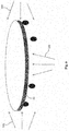
- FIG. 3 is a diagrammatic fragmentary cross-sectional side view of a semiconductor wafer 45 in accordance with various aspects of the present disclosure.
- the semiconductor wafer 45 may include an integrated circuit (IC) chip, system on chip (SoC), or portion thereof, and may include various passive and active microelectronic devices such as resistors, capacitors, inductors, diodes, metal-oxide semiconductor field effect transistors (MOSFET), complementary metal-oxide semiconductor (CMOS) transistors, bipolar junction transistors (BJT), laterally diffused MOS (LDMOS) transistors, high power MOS transistors, or other types of transistors.
- IC integrated circuit
- SoC system on chip
- various passive and active microelectronic devices such as resistors, capacitors, inductors, diodes, metal-oxide semiconductor field effect transistors (MOSFET), complementary metal-oxide semiconductor (CMOS) transistors, bipolar junction transistors (BJT), laterally diffused MOS (LDMOS) transistors, high power MOS
- a semiconductor wafer 45 includes a substrate 48 .
- the substrate 48 is a silicon substrate doped with a p-type dopant such as boron (for example a p-type substrate).
- the substrate 48 could be another suitable semiconductor material.
- the substrate 48 may be a silicon substrate that is doped with an n-type dopant such as phosphorous or arsenic (an n-type substrate).
- the substrate 48 could include other elementary semiconductors such as germanium and diamond.
- the substrate 48 could optionally include a compound semiconductor and/or an alloy semiconductor.
- the substrate 48 could include an epitaxial layer (epi layer), may be strained for performance enhancement, and may include a silicon-on-insulator (SOI) structure.
- epi layer epitaxial layer
- SOI silicon-on-insulator
- the substrate 48 is substantially conductive or semi-conductive.
- the electrical resistance may be less than about 10 3 ohm-meter.
- the substrate 48 contains metal, metal alloy, or metal nitride/sulfide/selenide/oxide/silicide with the formula MXa, where M is a metal, and X is N, S, Se, O, Si, and where “a” is in a range from about 0.4 to 2.5.
- the substrate 48 may contain Ti, Al, Co, Ru, TiN, WN2, or TaN.
- the substrate 48 contains a dielectric material with a dielectric constant in a range from about 1 to about 40.
- the substrate 48 contains Si, metal oxide, or metal nitride, where the formula is MXb, wherein M is a metal or Si, and X is N or O, and wherein “b” is in a range from about 0.4 to 2.5.
- the substrate 48 may contain SiO 2 , silicon nitride, aluminum oxide, hafnium oxide, or lanthanum oxide.
- a material layer 50 is formed over the substrate 48 .
- the material layer 50 can be patterned via a lithography process and as such may also be referred to as a patternable layer.
- the material layer 50 includes a dielectric material, such as silicon oxide or silicon nitride.
- the material layer 50 includes metal.
- the material layer 50 includes a semiconductor material.
- the material layer 50 has different optical properties than photoresist.
- the material layer 50 has a different n, k, or T value from photoresist.
- the material layer 50 comprises at least one of different polymer structure, acid labile molecule, PAG (photo acid generator), quencher, chromophore, cross linker, or solvent, which lead to different n value to photoresist.
- the material layer 50 and photoresist have different etching resistance.
- the material layer 50 contains an etching resistant molecule. The molecule includes low onishi number structure, double bond, triple bond, silicon, silicon nitride, Ti, TiN, Al, aluminum oxide, SiON, or combinations thereof.
- substrate 48 and the material layer 50 may each include additional suitable material compositions in other embodiments.
- a photoresist layer 60 is formed over the material layer 50 .
- the photoresist layer 60 includes a positive photoresist, but it is understood that the photoresist layer 60 may be a negative photoresist in alternative embodiments.
- the photoresist layer 60 may be formed by a spin-coating process.
- the photoresist layer 60 contains components such as a polymer, photo acid generators (PAG), quenchers, chromophore, surfactant, cross linker, etc.
- the photo acid generator is bonded to the polymer. In a subsequent photolithography process, photons induce decomposition of the PAG.
- the photoresist layer 60 may also optionally include a quencher that is disposed within the photoresist layer 60 in order to improve critical dimension (CD) control.
- CD critical dimension
- the photoresist layer 60 contains a photo-acid generator (PAG).
- the photo-acid generator includes an acid generator component and a sensitizer component.
- the sensitizer component is also referred to as a sensitizer moiety, and it is bonded or linked to the acid generator through a linker.
- the photoresist layer 60 may be a tri-layer photoresist.
- a tri-layer photoresist may include a bottom layer (also referred to as an under layer), a middle layer, and a top layer (the top layer may also be referred to as a PR layer).
- the bottom layer includes a CxHyOz material
- the middle layer includes a SiCxHyOz material
- the top layer includes a CxHyOz material.
- the CxHyOz material of the bottom layer may be identical to the CxHyOz material of the top layer in some embodiments, but they may also be different in other embodiments.
- the top layer also includes a photo-sensitive element, such as a photo-acid generator (PAG).
- PAG photo-acid generator
- the top layer is patterned by a photolithography process, which may include one or more exposure, baking, developing, and rinsing processes (not necessarily performed in this order).
- the photolithography process patterns the top layer into a photoresist mask, which may have one or more trenches or openings that expose the middle layer therebelow.
- the middle layer is then etched using the photoresist mask to form a patterned middle layer, and the bottom layer is then etched using the patterned middle layer to form a patterned bottom layer.
- the patterned bottom layer is then used to pattern the various layers below.
- the photoresist layer 60 shown in FIG. 3 has metal-containing (or metal-compound-containing) material 70 added therein.
- the metal-containing material 70 includes Caesium (Cs), Barium (Ba), Lanthanum (La), Indium (In), Cerium (Ce), Silver (Ag), or Tin (Sn), or combinations or compounds thereof.
- the metal-containing material 70 may be located in any one of the bottom layer, the middle layer, the top layer, or in all of these layers.
- the metal-containing material 70 helps enhance the photon absorption in EUV lithography. However, as discussed above, the metal-containing material 70 may cause contamination problems. Therefore, the present disclosure will remove the metal-containing particles after (or during) the photoresist layer 60 has been used to perform EUV lithography patterning.
- FIG. 4 illustrates a flow of cleaning the wafer 45 to remove the contaminant metal-containing material 70 according to an embodiment of the present disclosure.
- a material 80 is dispensed on the wafer 45 .
- the material 80 may include a photoresist specifically configured for EUV lithography, which as discussed above includes a metal-containing material such as the metal-containing material 70 shown in FIG. 3 .
- the material 80 may also include a developer solution that is used to develop the photoresist.
- a cleaning fluid 100 is applied to the wafer 45 to remove the metal-containing material 70 .
- the cleaning fluid 100 is applied to a back side of the wafer 45 and/or the side edges of the wafer 45 .
- the wafer transferring process e.g., as the wafer 45 is transferred out of the one semiconductor fabrication tool to another semiconductor fabrication tool
- the wafer transferring process may involve physical contact with the back side or the side edges of the wafer 45 .
- various components of the semiconductor fabrication tool may come into contact with the bottom (e.g., back side) or side portions of the wafer 45 . Through such contact, the metal-containing material 70 ( FIG. 3 ) may be left on the semiconductor fabrication tool. If a subsequent process performed by that semiconductor fabrication tool is supposed to be metal-free, then the metal-containing material 70 may be considered a contaminant.
- the metal-containing material 70 may contaminate a new semiconductor fabrication tool as the wafer is loaded into the new semiconductor fabrication tool. This may be exacerbated by various heating processes, which facilitate the escape of the metal-containing material 70 from the wafer 45 .
- the new (and now contaminated) semiconductor fabrication tool may be intended to perform a semiconductor fabrication process in a metal-free environment, in which case the presence of the metal-containing material 70 therein is undesirable.
- the metal-containing material 70 is cleaned off using the cleaning fluid 100 .
- the cleaning fluid 100 is configured to mostly target the back side and the side edges of the wafer 45 , although the front side of the 45 may be optionally cleaned as well.
- the cleaning fluid 100 contains a solvent that is selected to have specific ranges with respect to Hansen solubility parameters of delta D, delta P, and delta H.
- Hansen solubility parameters provide a way to predict whether one material will dissolve in another and form a solution.
- a molecule of a given material has three Hansen parameters (each generally measured in MPa 0.5 ) delta D, delta P, and delta H.
- Delta D is the energy from dispersion forces between molecules.
- Delta P is the energy from dipolar intermolecular force between molecules.
- Delta H is the energy from hydrogen bonds between molecules.
- the solvent is configured to have specific ranges of Hansen parameters so that the metal-containing material 70 can be easily dissolved and consequently removed.
- the solvent's Hansen parameters are such that a delta D is in a range from 13 to 25, a delta P is in a range from 3 to 25, and a delta H is in a range from 4 to 30.
- the solvent's Hansen parameters are such that a delta D is in a range from 15 to 22, a delta P is in a range from 3.5 to 17, and a delta H is in a range from 5 to 16.
- the solvent is an aqueous solvent.
- a water-soluble acid or water-soluble base may be added to the aqueous solvent to enhance the ability of the solvent in removing the metal-containing material 70 .
- the concentration of the acid or base in the aqueous solvent may be in a range from 0.001% to 30%, for example in a range between 0.1% and 20%. In some embodiments, the concentration of the acid or base in the aqueous solvent is in a range from 0.1% to 10%.
- a pka acid dissociation constant, also referred to an acidity constant or acid-ionization constant, which is a logarithmic value herein
- a pka acid dissociation constant, also referred to an acidity constant or acid-ionization constant, which is a logarithmic value herein
- Non-limiting examples of the aqueous acid may include H 2 SO 4 , HNO 3 , HCl, H 3 PO 4 , CCl 3 COOH, HBr, or combinations thereof. If a base is used, the pka of the base is in a range from 9 to 40, for example from 10-20.
- Non-limiting examples of the aqueous base may include NaOH, NH 3 , KOH, TMAH, TEAH, or combinations thereof.
- a metal chelate may be added to the aqueous solvent addition to, or instead of, the acid or base.
- the concentration of the metal chelate in the aqueous solvent may be in a range from 0.001% to 30%, for example in a range between 0.1% and 20%.
- the metal chelate may include ethylenediaminetetraacetic acid (EDTA), ethylenediamine-N, N′-disuccinic acid (EDDS), diethylenetriaminepentaacetic acid (DTPA), polyaspartic acid, trans-1, 2-Cyclohexanediamine-N, N, N′, N′-tetraacetic acid monohydrate, ethylenediamine, or combinations thereof.
- the aqueous solvent may also be heated to increase the cleaning efficiency.
- the aqueous solvent is heated in a temperature ranging between room temperature (e.g., 25 degrees Celsius) and 75 degrees Celsius, for example between 45 and 75 degrees Celsius.
- surfactants may also be added to the aqueous solvent to increase the solubility and/or to reduce the surface tension on the wafer 45 .
- the concentration of the surfactant in the aqueous solvent may be in a range from 0.1% to 5%. It is understood that the various ranges the materials discussed herein are configured to enhance the efficacy of the solvent, for example the efficacy with respect to cleaning the metal-containing material 70 off of the wafer 45 .
- the solvent is an organic solvent.
- the organic solvent may have a polar function, such as —OH, —COOH, —CO—, —O—, —COOR, —CN—, —SO—, as non-limiting examples.
- the organic solvent may include PGME, PGEE, GBL, CHN, EL, Methanol, Ethanol, Propanol, n-Butanol, Acetone, DMF, Acetonitrile, IPA, THF, Acetic acid, or combinations thereof.
- An organic acid or organic base may be added to the organic solvent to enhance the ability of the solvent in removing the metal-containing material 70 .
- the concentration of the acid or base in the organic solvent may be in a range from 0.001% to 30%, for example in a range between 0.1% and 20%. If an acid is used, a pka (acid dissociation constant, also referred to an acidity constant or acid-ionization constant, which is a logarithmic value herein) of the acid is in a range from ⁇ 11 to 4.
- a pka acid dissociation constant, also referred to an acidity constant or acid-ionization constant, which is a logarithmic value herein
- Non-limiting examples of the organic acid may include ethanedioic acid, methanoic acid, 2-hydroxypropanoic acid, 2-hydroxybutanedioic acid, citric acid, uric acid, trifluoromethanesulfonic acid, benzenesulfonic acid, ethanesulfonic acid, methanesulfonic acid, oxalic acid dihydrate, maleic acid, or combinations thereof.
- the pka of the base is in a range from 9 to 40.
- the organic base may include monoethanolamine, monoisopropanolamine, 2-amino-2-methyl-1-propanol, 1H-benzotriazole, 1, 4-triazole, 1, 8-diazabicycloundec-7-ene or combinations thereof.
- a metal chelate may be added to the organic solvent addition to, or instead of, the acid or base. In these embodiments, the concentration of the metal chelate in the organic solvent may be in a range from 0.001% to 30%.
- Non-limiting examples of the metal chelate may include ethylenediaminetetraacetic acid EDTA), ethylenediamine-N, N′-disuccinic acid (EDDS), diethylenetriaminepentaacetic acid (DTPA), polyaspartic acid, trans-1, 2-Cyclohexanediamine-N, N, N′, N′-tetraacetic acid monohydrate, ethylenediamine, or combinations thereof.
- the organic solvent may also be heated to increase the cleaning efficiency.
- the organic solvent is heated in a temperature ranging between room temperature (e.g., 25 degrees Celsius) and 75 degrees Celsius.
- surfactants may also be added to the organic solvent to increase the solubility and/or to reduce the surface tension on the wafer 45 .
- concentration of the surfactant in the organic solvent may be in a range from 0.1% to 5%. It is understood that the various ranges the materials discussed herein are configured to enhance the efficacy of the solvent, for example the efficacy with respect to cleaning the metal-containing material 70 off of the wafer 45 .
- FIGS. 5-6 illustrate a flow of cleaning the wafer 45 to remove the contaminant (e.g., the metal-containing material 70 ) according to an alternative embodiment of the present disclosure.
- the material 80 is dispensed on the wafer 45 .
- the material 80 may include a metal-containing photoresist specifically configured for EUV lithography (for better photon absorption), and/or it may also include a developer solution. While the material 80 is applied on the wafer 45 , the cleaning fluid 100 is not applied yet.
- the cleaning fluid 100 is applied to the wafer 45 to remove the metal-containing material 70 .
- the cleaning fluid 100 is mostly applied to a back side of the wafer 45 and/or the side edges of the wafer 45 , and may be optionally applied to the front side of the wafer 45 in some embodiments.
- the cleaning fluid 100 includes an aqueous or organic solvent having a particular range of Hansen solubility parameters to facilitate the removal of the metal-containing material 70 .
- Various additives such as acid, base, or metal chelate may also be added to the solvent as discussed above, to further enhance the efficacy of the cleaning fluid 100 in removing the metal-containing material 70 .
- the flow corresponding to FIG. 4 is configured to remove the metal-containing material 70 as the metal-containing material 70 is being dispensed (in the photoresist)
- the flow corresponding to FIGS. 5-6 is configured to remove the metal-containing material 70 via an extra cleaning step.
- the cleaning system 150 may be a part of an existing semiconductor fabrication apparatus, for example it may be integrated into an EUV lithography tool where metal-containing photoresist is used for EUV lithography. In other embodiments, the cleaning system 150 may be a part of other types of semiconductor fabrication equipment where metal contaminants may be introduced.
- the material 80 e.g., a metal-containing EUV photoresist and/or a developer solution
- the metal in the material 80 may be considered a contaminant and will be removed by the cleaning system 150 , as discussed below.
- the cleaning system 150 includes a chamber 160 in which the wafer 45 is disposed.
- the chamber is sealable so as to isolate the wafer 45 from other potential contaminants outside the chamber 160 .
- the cleaning system 150 may also include one or more exhaust mechanisms 170 that are coupled to the chamber 160 such that fluids (e.g., air, which may include contaminant particles) from inside the chamber 160 may be “sucked” out of the chamber 160 .
- fluids e.g., air, which may include contaminant particles
- a negative pressure is applied to the exhaust mechanisms 170 to create at least a partial vacuum inside or near the exhaust mechanisms 170 .
- the negative pressure applied to the exhaust mechanisms 170 will force the fluids such as air inside the chamber 160 to flow toward, and then out of, the exhaust mechanisms 170 .
- the cleaning system 150 further includes a plurality of nozzles 180 and 181 that are each configured to spray the cleaning fluid 100 discussed above with reference to FIGS. 4-6 .
- the nozzle 180 is positioned below the wafer 45 and is therefore configured to spray the cleaning fluid 100 onto the back side of the wafer 45 .
- the nozzle 181 is positioned near a side edge of the wafer 45 and is therefore configured to spray the cleaning fluid 100 onto the side edge of the wafer 45 .
- the cleaning system 150 may include other nozzles that are also configured to spray the cleaning fluid 100 onto the wafer 45 .
- more than one nozzle may be positioned below the wafer 45
- more than one nozzle may be positioned around different side edge points of the wafer 45
- one or more nozzles may also be positioned above the wafer 45 to spray the cleaning fluid 100 onto the front side of the wafer 45 .
- the cleaning fluid 100 sprayed by the nozzles 180 - 181 (and other similar nozzles) herein will wash the metal-containing material 70 away from the wafer 45 , for example away from the back surface and the side surfaces of the wafer 45 .
- the cleaning system 150 also includes nozzles 190 and 191 that are each configured to deliver a suitable purging fluid 200 (e.g., air) to the wafer 45 .
- a suitable purging fluid 200 e.g., air
- the nozzle 190 is positioned below the wafer 45 and is therefore configured to apply the purging fluid 200 onto the back side of the wafer 45 .
- the nozzle 191 is positioned near a side edge of the wafer 45 and is therefore configured to spray the purging fluid 200 onto the side edge of the wafer 45 . Positive pressure is applied through the nozzles 190 - 191 to ensure that the purging fluid 200 spurts out of the nozzles 190 - 191 and makes contact with the wafer 45 .
- a magnitude (or absolute value) of the positive pressure applied through the nozzles 190 - 191 exceeds the magnitude (or absolute) value of the negative pressured applied through the nozzles 180 - 181 .
- the purging fluid 200 includes clean dry air (CDA). In other embodiments, the purging fluid 200 includes nitrogen. In yet other embodiments, the purging fluid 200 includes another suitable material that does not react with films on the wafer 45 .
- the interaction between the purging fluid 200 and the wafer enhances the effectiveness of the washing or the removal of contaminant particles, including the removal of the metal-containing material 70 .
- the nozzles 190 - 191 “pushes”, and the exhaust mechanisms 170 “pulls” the metal containing-material 70 off of the wafer 45 and out of the chamber 160 .
- the cleaning system 150 may include other nozzles that are also configured to deliver the purging fluid 200 onto the wafer 45 ,
- more than one nozzle may be positioned below the wafer 45
- more than one nozzle may be positioned around different side edge points of the wafer 45
- one or more nozzles may also be positioned above the wafer 45 to deliver the purging fluid 200 onto the front side of the wafer 45 .
- a respective purging fluid nozzle e.g., nozzles 190 - 191
- a respective cleaning fluid nozzle e.g., nozzles 180 - 181 .
- the purging fluid 200 delivered by the nozzles 190 - 191 (and other similar nozzles) herein will help wash the metal-containing material 70 away from the wafer 45 , for example away from the back surface and the side surfaces of the wafer 45 .
- the cleaning system 150 also has mechanisms in place to spin the wafer 45 during the cleaning process, such as during the application of the cleaning fluid 100 and/or the purging fluid 200 .
- the cleaning system 150 may include a spinner apparatus 250 .
- the spinner apparatus 250 may include a chuck, a pedestal, and/or a motor.
- the spinner apparatus is mechanically coupled to the wafer 45 , and it is configured to rotate or spin in a clockwise and/or a counterclockwise manner. Thus, as the spinner apparatus 250 rotates or spins, so does the wafer 45 .
- the cleaning system 150 may include a controller 300 that is communicatively coupled to the spinner apparatus 250 .
- the controller 300 may be remotely located (or locally located) from the rest of the cleaning system 150 .
- the controller 300 may be implemented outside the chamber 160 in some embodiments, and it may be implemented inside the chamber 160 in other embodiments.
- the controller 300 may also be a part of an overall semiconductor manufacturing system, of which the cleaning system 150 is a part.
- the controller 300 may include electronic memory and one or more electronic processors configured to execute programming instructions stored in the electronic memory, which may involve a program controlling the spin of the spinner apparatus 250 .
- the controller 300 controls the spinner apparatus (and therefore the wafer 45 ) to rotate or spin according to a specific spin speed, spin duration, and/or a spin direction (e.g., clockwise or counterclockwise).
- the controller 300 is configured to set a spin rate/speed of the wafer in a range between about 800 RPM to about 4500 RPM, for example between about 800 RPM and about 3500 RPM. This range of the spin speed is optimized to enhance the distribution of the cleaning fluid 100 on the wafer 45 and to facilitate the removal of the contaminant materials such as the metal-containing material 70 .
- the spinning of the wafer 45 need not be only in one direction. Instead of performing the spin in just a clockwise direction or just in a counterclockwise direction, the wafer 45 (under the control of the controller 300 ) may undergo a combination of clockwise and counterclockwise spins.
- the wafer 45 may be configured to spin in a clockwise direction for an X number of seconds, followed by a spin in the counterclockwise direction for a Y number of seconds (where Y may be the same as X or may be different), or vice versa.
- the combination of performing clockwise spins and counterclockwise spins in an alternating manner may further enhance the application of the cleaning fluid 100 and the purging fluid 200 with respect to the wafer 45 , thereby improving the removal of the metal-containing materials as contaminants.
- FIG. 8 provides a visual illustration of a flow in which the cleaning process is performed according to embodiments of the present disclosure.
- the lithography process 400 is an EUV lithography process.
- the lithography process 400 includes a step 410 in which a photo-sensitive material is coated onto a wafer such as the wafer 45 .
- the photo-sensitive material lay include a tri-layer photoresist (including a top layer (PR), a middle layer (ML), and an under layer (UL)).
- the photo-sensitive material may be coated via a spin-coating process.
- the photo-sensitive material contains metal, which are considered contaminants after the lithography process is performed and should be removed.
- the lithography process 400 includes a step 420 of pre-exposure baking, in which the wafer (and the metal-containing photo-sensitive material coated thereon) is baked.
- the lithography process 400 includes a step 430 of exposure, in which the wafer (and the metal-containing photo-sensitive material coated thereon) is exposed. In some embodiments, the exposure involves using ultraviolet (UV) light or using e-beam to expose the wafer 45 .
- the lithography process 400 includes a step 440 of post-exposure bake, in which the wafer 45 (and the metal-containing photo-sensitive material coated thereon) is baked.
- the lithography process 400 includes a step 450 of developing, in which the wafer (and the metal-containing photo-sensitive material coated thereon) is developed via an application of a developer solution onto the wafer. It is understood that the lithography process 400 may include additional processes that are not specifically illustrated or discussed herein.
- the wafer 45 is cleaned, using the cleaning system 150 discussed above with reference to FIG. 7 , while the steps 410 and 450 are performed.
- the wafer 45 is cleaned using the cleaning system 150 .
- the wafer 45 is also cleaned using the cleaning system 150 . It is understood, however, that according to this process flow, the wafer 45 need not necessarily be cleaned twice.
- the wafer 45 may be cleaned just during the step 410 , or alternatively it may be cleaned just during the step 450 , but not necessarily during both steps 410 and 450 .
- FIG. 9 provides another visual illustration of another flow in which the cleaning process is performed according to embodiments of the present disclosure. For reasons of consistency and clarity, similar elements appearing in FIGS. 8-9 are labeled the same.
- the process flow shown in FIG. 9 performs the wafer cleaning after the steps 410 , 420 , 440 , and 450 , rather than during the steps 410 and 450 .
- the wafer 45 may be cleaned (using the cleaning system 150 ) after the metal-containing photo-sensitive material has been coated onto the wafer, and/or after the pre-exposure baking process, and/or after the post-exposure baking process, and/or after the developing process.
- the wafer 45 need not necessarily be cleaned four times in this process flow.
- the wafer 45 may be cleaned (using the cleaning system 150 ) just after any one of the steps 410 , 420 , 440 , and 450 , or combinations thereof.
- a flow A includes a step 510 of performing a high-contact-angle material rinsing process to the wafer, for example the wafer 45 discussed above.
- the rinse may be applied to a backside or an edge of the wafer.
- the high-contact-angle material may include a material that has a contact angle that is greater than 75% with respect to water. After the wafer surface is treated with the high-contact-angle material, the wafer surface becomes hydrophobic.
- the hydrophobicity of the wafer surface (due to the application of the high-contact-angle material in step 510 ) allows the metal-containing material in the photoresist to be more easily washed off of the wafer.
- a step 520 is performed after the high-contact-angle material rinse step of 510 .
- a metallic film is dispensed.
- the metallic film may be the metal-containing material in the photoresist discussed above.
- step 520 may involve coating a metal-containing photoresist material on the wafer surface.
- a step 530 is performed after the step 520 .
- the step 530 involves a new solvent rinsing process,
- the new solvent may be embodiments of the cleaning fluid 100 discussed above, for example containing a solvent with the specified ranges of Hansen parameters.
- the step 530 allows the metal-containing material to be washed off of the wafer, which reduces risks of contamination.
- Flows B and C are similar to flow A.
- another step 540 is performed, in which a commercial solvent rinsing process is performed to the wafer.
- the commercial solvent may include other commonly used solvents in the industry in a photolithography process.
- the difference between flows B and C is that, the step 540 (commercial solvent rinsing) is performed after the step 530 in flow B, but it is performed before the step 530 in flow C.
- the high-contact-angle material includes a carbon fluoride compound, for example a C x F y unit.
- x is in a range between 1 and 7, and y is saturated by structure.
- This carbon fluoride compound may be in the form of an additive that is added to a solvent.
- the carbon fluoride compound is a polymer.
- the carbon fluoride compound may be branched in some embodiments, but unbranched in other embodiments.
- the carbon fluoride compound may also be cyclic in some embodiments, but uncyclic in other embodiments.
- the carbon fluoride compound may be saturated with hydrogen or halogen atom.
- the polymer chain may include polystyrene, acrylate, or a 1 ⁇ 10 carbon unit to form a polymer.
- the polymer may be within a C x F y monomer.
- FIG. 11 is a flowchart of a method 600 of performing a semiconductor fabrication process according to various aspects of the present disclosure.
- the method 600 includes a step 610 of forming a patternable layer over a substrate.
- the substrate is substantially conductive or semi-conductive.
- the electrical resistance may be less than about 10 3 ohm-meter.
- the substrate contains metal, metal alloy, or metal nitride/sulfide/selenide/oxide/silicide with the formula MXa, where M is a metal, and X is N, S, Se, O, Si, and where “a” is in a range from about 0.4 to 2.5.
- the substrate 48 may contain Ti, Al, Co, Ru, TiN, WN 2 , or TaN.
- the substrate contains a dielectric material with a dielectric constant in a range from about 1 to about 40.
- the substrate contains Si, metal oxide, or metal nitride, where the formula is MXb, wherein M is a metal or Si, and X is N or O, and wherein “b” is in a range from about 0.4 to 2.5.
- the substrate may contain SiO 2 , silicon nitride, aluminum oxide, hafnium oxide, or lanthanum oxide.
- the patternable layer formed over the substrate has different optical properties than photoresist.
- the patternable layer has a different n, k, or T value from photoresist.
- the layer comprises at least one of different polymer structure, acid labile molecule, PAG (photo acid generator) loading, quencher loading, chromophore, cross linker, or solvent, which lead to different n value to photoresist.
- the patternable layer and photoresist have different etching resistance.
- the patternable layer contains an etching resistant molecule. The molecule includes low onishi number structure, double bond, triple bond, silicon, silicon nitride, Ti, TiN, Al, aluminum oxide, SiON, or combinations thereof.
- the method 600 includes a step 620 of coating a photoresist layer over the patternable layer.
- the photoresist layer includes a metal-containing material.
- the method 600 includes a step 630 of performing a lithography process to the photoresist layer to form a patterned photoresist.
- the lithography process includes an extreme ultraviolet (EUV) lithography process.
- EUV extreme ultraviolet
- the method 600 includes a step 640 of cleaning the wafer with a cleaning fluid to remove the metal-containing material.
- the cleaning fluid includes a solvent having Hansen solubility parameters of delta. D in a range between 13 and 25, delta P in a range between 3 and 25, and delta H in a range between 4 and 30.
- the solvent is an aqueous solvent.
- the solvent is an organic solvent.
- the solvent contains an acid with an acid dissociation constant (pka) less than 4, for example between ⁇ 11 and 4.
- the solvent contains a base with an acid dissociation constant (pka) greater than 9, for example between 9 and 40.
- the solvent contains a metal chelate.
- the solvent contains a surfactant.
- the solvent is heated to a temperature ranging between room temperature and 75 degrees Celsius.
- the cleaning the wafer comprises spinning the wafer as the wafer is being cleaned.
- the cleaning the wafer comprises applying the cleaning fluid to at least one of: a back side of the wafer or a side edge of the wafer. In some embodiments, the cleaning the wafer comprises delivering a purging fluid to the wafer, the purging fluid being delivered to at least one of: a back side of the wafer or a side edge of the wafer.
- the performing the lithography process includes performing: a photoresist-coating process, a pre-exposure baking process, an exposure process, a post-exposure baking process, and a developing process. The cleaning the wafer may be performed while the photoresist-coating process or the developing process is performed. The cleaning the wafer may also be performed: after the photoresist-coating process, after the pre-exposure baking process, after the post-exposure baking process, or after the developing process.
- the present disclosure offers advantages over conventional methods. It is understood, however, that other embodiments may offer additional advantages, and not all advantages are necessarily disclosed herein, and that no particular advantage is required for all embodiments.
- One advantage is that the photoresist material herein offers improved lithography performance, for example better photon absorption performance due to the presence of metal or metal compounds in the photoresist.
- Another advantage is that the systems and methods of cleaning the wafer using the novel solvent herein as a cleaning fluid to wash the metal-containing material off the wafer) reduce contamination caused by the metal-containing material, for both the apparatus in which the lithography process is performed, and also for other semiconductor fabrication tools to which the wafer (after being cleaned) is transferred. For at least these reasons, the present disclosure improves semiconductor fabrication performance.
- One aspect of the present disclosure pertains to a method of fabricating a semiconductor device.
- a photoresist layer is coated over a wafer.
- the photoresist layer includes a metal-containing material.
- a lithography process is performed to the photoresist layer to form a patterned photoresist.
- the wafer is cleaned with a cleaning fluid to remove the metal-containing material.
- a photoresist layer is coated over a wafer.
- the photoresist layer includes a metal-containing material.
- An extreme ultraviolet (EUV) lithography process is performed to the photoresist layer to form a patterned photoresist.
- the wafer is cleaned with a cleaning fluid to remove the metal-containing material.
- the cleaning fluid includes a solvent having Hansen solubility parameters of delta D in a range between 13 and 25, delta P in a range between 3 and 25, and delta H in a range between 4 and 30.
- the solvent contains an acid with an acid dissociation constant less than 4 or a base with an acid dissociation constant greater than 9.
- the system includes a chamber configured to coat a metal-containing photoresist material onto a wafer as a part of an EUV lithography process.
- the system includes one or more first nozzles configured to apply a cleaning fluid to the wafer.
- the cleaning fluid has a material composition configured for removing a metal contaminant from the wafer.
- the metal contaminant arises from the metal-containing photoresist material.
- the system includes one or more second nozzles configured to apply a purging fluid to the wafer. The purging fluid facilitates a removal of the metal contaminant from the wafer.
Abstract
Description
Claims (20)
Priority Applications (6)
| Application Number | Priority Date | Filing Date | Title |
|---|---|---|---|
| US15/351,529 US10866516B2 (en) | 2016-08-05 | 2016-11-15 | Metal-compound-removing solvent and method in lithography |
| US15/491,066 US10622211B2 (en) | 2016-08-05 | 2017-04-19 | Metal-compound-removing solvent and method in lithography |
| TW106124968A TWI709442B (en) | 2016-08-05 | 2017-07-25 | A method of manufacturing semiconductor device |
| CN201710660773.6A CN107689322B (en) | 2016-08-05 | 2017-08-04 | Method and system for manufacturing semiconductor device |
| US17/121,261 US11681226B2 (en) | 2016-08-05 | 2020-12-14 | Metal-compound-removing solvent and method in lithography |
| US18/336,399 US20230324806A1 (en) | 2016-08-05 | 2023-06-16 | Metal-Compound-Removing Solvent And Method In Lithography |
Applications Claiming Priority (2)
| Application Number | Priority Date | Filing Date | Title |
|---|---|---|---|
| US201662371324P | 2016-08-05 | 2016-08-05 | |
| US15/351,529 US10866516B2 (en) | 2016-08-05 | 2016-11-15 | Metal-compound-removing solvent and method in lithography |
Related Child Applications (2)
| Application Number | Title | Priority Date | Filing Date |
|---|---|---|---|
| US15/491,066 Continuation-In-Part US10622211B2 (en) | 2016-08-05 | 2017-04-19 | Metal-compound-removing solvent and method in lithography |
| US17/121,261 Continuation US11681226B2 (en) | 2016-08-05 | 2020-12-14 | Metal-compound-removing solvent and method in lithography |
Publications (2)
| Publication Number | Publication Date |
|---|---|
| US20180039182A1 US20180039182A1 (en) | 2018-02-08 |
| US10866516B2 true US10866516B2 (en) | 2020-12-15 |
Family
ID=61069207
Family Applications (3)
| Application Number | Title | Priority Date | Filing Date |
|---|---|---|---|
| US15/351,529 Active 2037-10-05 US10866516B2 (en) | 2016-08-05 | 2016-11-15 | Metal-compound-removing solvent and method in lithography |
| US17/121,261 Active 2037-07-28 US11681226B2 (en) | 2016-08-05 | 2020-12-14 | Metal-compound-removing solvent and method in lithography |
| US18/336,399 Pending US20230324806A1 (en) | 2016-08-05 | 2023-06-16 | Metal-Compound-Removing Solvent And Method In Lithography |
Family Applications After (2)
| Application Number | Title | Priority Date | Filing Date |
|---|---|---|---|
| US17/121,261 Active 2037-07-28 US11681226B2 (en) | 2016-08-05 | 2020-12-14 | Metal-compound-removing solvent and method in lithography |
| US18/336,399 Pending US20230324806A1 (en) | 2016-08-05 | 2023-06-16 | Metal-Compound-Removing Solvent And Method In Lithography |
Country Status (1)
| Country | Link |
|---|---|
| US (3) | US10866516B2 (en) |
Cited By (1)
| Publication number | Priority date | Publication date | Assignee | Title |
|---|---|---|---|---|
| US20210103220A1 (en) * | 2016-08-05 | 2021-04-08 | Taiwan Semiconductor Manufacturing Co., Ltd. | Metal-Compound-Removing Solvent and Method in Lithography |
Families Citing this family (10)
| Publication number | Priority date | Publication date | Assignee | Title |
|---|---|---|---|---|
| WO2019059074A1 (en) * | 2017-09-19 | 2019-03-28 | Jsr株式会社 | Resist pattern forming method and substrate treatment method |
| CN109324484B (en) * | 2018-09-27 | 2020-03-27 | 武汉华星光电技术有限公司 | Developing unit cleaning device and cleaning method using the same |
| US11605538B2 (en) * | 2018-10-31 | 2023-03-14 | Taiwan Semiconductor Manufacturing Co., Ltd. | Protective composition and method of forming photoresist pattern |
| WO2020102085A1 (en) | 2018-11-14 | 2020-05-22 | Lam Research Corporation | Methods for making hard masks useful in next-generation lithography |
| US11456170B2 (en) * | 2019-04-15 | 2022-09-27 | Taiwan Semiconductor Manufacturing Co., Ltd. | Cleaning solution and method of cleaning wafer |
| US20230185196A1 (en) * | 2020-04-03 | 2023-06-15 | Lam Research Corporation | Pre-exposure photoresist curing to enhance euv lithographic performance |
| WO2022016126A1 (en) * | 2020-07-17 | 2022-01-20 | Lam Research Corporation | Metal chelators for development of metal-containing photoresist |
| KR20230152171A (en) * | 2020-11-13 | 2023-11-02 | 램 리써치 코포레이션 | Process tool for dry removal of photoresist |
| US11846886B2 (en) * | 2020-11-23 | 2023-12-19 | International Business Machines Corporation | Photoacid generator |
| US11769662B2 (en) * | 2021-03-19 | 2023-09-26 | Taiwan Semiconductor Manufacturing Company, Ltd. | Method for reducing charging of semiconductor wafers |
Citations (42)
| Publication number | Priority date | Publication date | Assignee | Title |
|---|---|---|---|---|
| US6184148B1 (en) * | 1986-05-29 | 2001-02-06 | Fujitsu Limited | Method for stripping a photo resist on an aluminum alloy |
| US20010012869A1 (en) * | 1998-10-22 | 2001-08-09 | Motoo Fukushima | Polysilane composition for forming a coating suitable for bearing a metal pattern, metal pattern forming method, wiring board preparing method |
| US20060103818A1 (en) | 2004-11-18 | 2006-05-18 | International Business Machines Corporation | Method and apparatus for cleaning a semiconductor substrate in an immersion lithography system |
| US20070091287A1 (en) | 2005-10-24 | 2007-04-26 | Taiwan Semiconductor Manufacturing Company, Ltd. | Immersion lithography apparatus and methods |
| US8216767B2 (en) | 2009-09-08 | 2012-07-10 | Taiwan Semiconductor Manufacturing Company, Ltd. | Patterning process and chemical amplified photoresist with a photodegradable base |
| US8323870B2 (en) | 2010-11-01 | 2012-12-04 | Taiwan Semiconductor Manufacturing Company, Ltd. | Method and photoresist with zipper mechanism |
| US20130202992A1 (en) | 2012-02-08 | 2013-08-08 | Taiwan Semiconductor Manufacturing Company, Ltd. | Mask and method for forming the mask |
| US20130296214A1 (en) * | 2010-07-16 | 2013-11-07 | Advanced Technology Materials, Inc. | Aqueous cleaner for the removal of post-etch residues |
| US8580117B2 (en) | 2007-03-20 | 2013-11-12 | Taiwan Semiconductor Manufactuing Company, Ltd. | System and method for replacing resist filter to reduce resist filter-induced wafer defects |
| US20130323641A1 (en) | 2012-06-01 | 2013-12-05 | Taiwan Semiconductor Manufacturing Company, Ltd., ("Tsmc") | Photosenstive material and method of lithography |
| US20140011133A1 (en) | 2012-07-05 | 2014-01-09 | Taiwan Semiconductor Manufacturing Company, Ltd. | Materials and methods for improved photoresist performance |
| US8628897B1 (en) | 2012-07-05 | 2014-01-14 | Taiwan Semiconductor Manufacturing Company, Ltd. | Extreme ultraviolet lithography process and mask |
| US20140017615A1 (en) | 2012-07-11 | 2014-01-16 | Taiwan Semiconductor Manufacturing Company, Ltd. | Apparatus and method for resist coating and developing |
| US20140017616A1 (en) | 2012-07-13 | 2014-01-16 | Taiwan Semiconductor Manufacturing Company, Ltd. | Apparatus and method for developing process |
| US20140038423A1 (en) * | 2012-08-02 | 2014-02-06 | Tokyo Electron Limited | Coating treatment method and coating treatment apparatus |
| US20140065843A1 (en) | 2012-09-04 | 2014-03-06 | Taiwan Semiconductor Manufacturing Company, Ltd | Method of Forming a Photoresist Layer |
| US8679707B2 (en) | 2012-08-01 | 2014-03-25 | Taiwan Semiconductor Manufacturing Company, Ltd. | Method of fabricating a lithography mask |
| US8691476B2 (en) | 2011-12-16 | 2014-04-08 | Taiwan Semiconductor Manufacturing Company, Ltd. | EUV mask and method for forming the same |
| US20140120459A1 (en) | 2012-11-01 | 2014-05-01 | Taiwan Semiconductor Manufacturing Company, Ltd. | Method for improving resist pattern peeling |
| US20140117563A1 (en) | 2011-07-27 | 2014-05-01 | Taiwan Semiconductor Manufacturing Company, Ltd. | Photoactive Compound Gradient Photoresist |
| US8715890B2 (en) | 2012-01-31 | 2014-05-06 | Taiwan Semiconductor Manufacturing Company, Ltd. | Semiconductor mask blanks with a compatible stop layer |
| US8715919B2 (en) | 2006-09-22 | 2014-05-06 | Taiwan Semiconductor Manufacturing Company, Ltd. | Surface switchable photoresist |
| US8722286B2 (en) | 2012-05-31 | 2014-05-13 | Taiwan Semiconductor Manufacturing Company, Ltd. | Devices and methods for improved reflective electron beam lithography |
| US8741551B2 (en) | 2012-04-09 | 2014-06-03 | Taiwan Semiconductor Manufacturing Company, Ltd. | Method and composition of a dual sensitive resist |
| US8753788B1 (en) | 2013-01-02 | 2014-06-17 | Taiwan Semiconductor Manufacturing Company, Ltd. | Apparatus of repairing a mask and a method for the same |
| US8764995B2 (en) | 2010-08-17 | 2014-07-01 | Taiwan Semiconductor Manufacturing Company, Ltd. | Extreme ultraviolet light (EUV) photomasks, and fabrication methods thereof |
| US8765582B2 (en) | 2012-09-04 | 2014-07-01 | Taiwan Semiconductor Manufacturing Company, Ltd. | Method for extreme ultraviolet electrostatic chuck with reduced clamp effect |
| US8765330B2 (en) | 2012-08-01 | 2014-07-01 | Taiwan Semiconductor Manufacturing Company, Ltd. | Phase shift mask for extreme ultraviolet lithography and method of fabricating same |
| US20140186773A1 (en) | 2013-01-02 | 2014-07-03 | Taiwan Semiconductor Manufacturing Company, Ltd. | Coating material and method for photolithography |
| US8785084B2 (en) | 2012-09-04 | 2014-07-22 | Taiwan Semiconductor Manufacturing Company, Ltd. | Method for mask fabrication and repair |
| US8828625B2 (en) | 2012-08-06 | 2014-09-09 | Taiwan Semiconductor Manufacturing Company, Ltd. | Extreme ultraviolet lithography mask and multilayer deposition method for fabricating same |
| US20140255850A1 (en) | 2013-03-09 | 2014-09-11 | Taiwan Semiconductor Manufacturing Company, Ltd. | Photo-Resist with Floating Acid |
| US20140272726A1 (en) | 2013-03-12 | 2014-09-18 | Taiwan Semiconductor Manufacturing Company, Ltd. | Photo Resist Baking in Lithography Process |
| US20140272709A1 (en) | 2013-03-14 | 2014-09-18 | Taiwan Semiconductor Manufacturing Company, Ltd. | Middle layer composition for trilayer patterning stack |
| US20140273521A1 (en) | 2013-03-12 | 2014-09-18 | Taiwan Semiconductor Manufacturing Company, Ltd. | Photoresist system and method |
| US8841047B2 (en) | 2012-04-02 | 2014-09-23 | Taiwan Semiconductor Manufacturing Company, Ltd. | Extreme ultraviolet lithography process and mask |
| US8877409B2 (en) | 2012-04-20 | 2014-11-04 | Taiwan Semiconductor Manufacturing Company, Ltd. | Reflective mask and method of making same |
| US20150192851A1 (en) * | 2013-12-05 | 2015-07-09 | Tokyo Ohka Kogyo Co., Ltd. | Negative resist composition, method of forming resist pattern, and complex |
| US20150286146A1 (en) | 2014-04-03 | 2015-10-08 | Taiwan Semiconductor Manufacturing Company, Ltd. | Systems and Methods for Improving Pattern Transfer |
| US20150311075A1 (en) | 2014-04-25 | 2015-10-29 | Taiwan Semiconductor Manufacturing Company, Ltd. | Method for Integrated Circuit Patterning |
| US20150309405A1 (en) | 2014-04-23 | 2015-10-29 | Taiwan Semiconductor Manufacturing Co., Ltd. | Method of making an extreme ultraviolet pellicle |
| US10622211B2 (en) * | 2016-08-05 | 2020-04-14 | Taiwan Semiconductor Manufacturing Co., Ltd. | Metal-compound-removing solvent and method in lithography |
Family Cites Families (3)
| Publication number | Priority date | Publication date | Assignee | Title |
|---|---|---|---|---|
| US4332879A (en) * | 1978-12-01 | 1982-06-01 | Hughes Aircraft Company | Process for depositing a film of controlled composition using a metallo-organic photoresist |
| JPH0713345A (en) * | 1993-06-21 | 1995-01-17 | Ricoh Co Ltd | Water shedding drying of base body for electrophotographic photoreceptor and device therefor |
| US10866516B2 (en) | 2016-08-05 | 2020-12-15 | Taiwan Semiconductor Manufacturing Co., Ltd. | Metal-compound-removing solvent and method in lithography |
-
2016
- 2016-11-15 US US15/351,529 patent/US10866516B2/en active Active
-
2020
- 2020-12-14 US US17/121,261 patent/US11681226B2/en active Active
-
2023
- 2023-06-16 US US18/336,399 patent/US20230324806A1/en active Pending
Patent Citations (44)
| Publication number | Priority date | Publication date | Assignee | Title |
|---|---|---|---|---|
| US6184148B1 (en) * | 1986-05-29 | 2001-02-06 | Fujitsu Limited | Method for stripping a photo resist on an aluminum alloy |
| US20010012869A1 (en) * | 1998-10-22 | 2001-08-09 | Motoo Fukushima | Polysilane composition for forming a coating suitable for bearing a metal pattern, metal pattern forming method, wiring board preparing method |
| US20060103818A1 (en) | 2004-11-18 | 2006-05-18 | International Business Machines Corporation | Method and apparatus for cleaning a semiconductor substrate in an immersion lithography system |
| US20070091287A1 (en) | 2005-10-24 | 2007-04-26 | Taiwan Semiconductor Manufacturing Company, Ltd. | Immersion lithography apparatus and methods |
| US8715919B2 (en) | 2006-09-22 | 2014-05-06 | Taiwan Semiconductor Manufacturing Company, Ltd. | Surface switchable photoresist |
| US8580117B2 (en) | 2007-03-20 | 2013-11-12 | Taiwan Semiconductor Manufactuing Company, Ltd. | System and method for replacing resist filter to reduce resist filter-induced wafer defects |
| US8216767B2 (en) | 2009-09-08 | 2012-07-10 | Taiwan Semiconductor Manufacturing Company, Ltd. | Patterning process and chemical amplified photoresist with a photodegradable base |
| US8658344B2 (en) | 2009-09-08 | 2014-02-25 | Taiwan Semiconductor Manufacturing Company, Ltd. | Patterning process and photoresist with a photodegradable base |
| US20130296214A1 (en) * | 2010-07-16 | 2013-11-07 | Advanced Technology Materials, Inc. | Aqueous cleaner for the removal of post-etch residues |
| US8764995B2 (en) | 2010-08-17 | 2014-07-01 | Taiwan Semiconductor Manufacturing Company, Ltd. | Extreme ultraviolet light (EUV) photomasks, and fabrication methods thereof |
| US8323870B2 (en) | 2010-11-01 | 2012-12-04 | Taiwan Semiconductor Manufacturing Company, Ltd. | Method and photoresist with zipper mechanism |
| US20140117563A1 (en) | 2011-07-27 | 2014-05-01 | Taiwan Semiconductor Manufacturing Company, Ltd. | Photoactive Compound Gradient Photoresist |
| US8691476B2 (en) | 2011-12-16 | 2014-04-08 | Taiwan Semiconductor Manufacturing Company, Ltd. | EUV mask and method for forming the same |
| US8715890B2 (en) | 2012-01-31 | 2014-05-06 | Taiwan Semiconductor Manufacturing Company, Ltd. | Semiconductor mask blanks with a compatible stop layer |
| US20130202992A1 (en) | 2012-02-08 | 2013-08-08 | Taiwan Semiconductor Manufacturing Company, Ltd. | Mask and method for forming the mask |
| US8709682B2 (en) | 2012-02-08 | 2014-04-29 | Taiwan Semiconductor Manufacturing Company, Ltd. | Mask and method for forming the mask |
| US8841047B2 (en) | 2012-04-02 | 2014-09-23 | Taiwan Semiconductor Manufacturing Company, Ltd. | Extreme ultraviolet lithography process and mask |
| US8741551B2 (en) | 2012-04-09 | 2014-06-03 | Taiwan Semiconductor Manufacturing Company, Ltd. | Method and composition of a dual sensitive resist |
| US8877409B2 (en) | 2012-04-20 | 2014-11-04 | Taiwan Semiconductor Manufacturing Company, Ltd. | Reflective mask and method of making same |
| US8722286B2 (en) | 2012-05-31 | 2014-05-13 | Taiwan Semiconductor Manufacturing Company, Ltd. | Devices and methods for improved reflective electron beam lithography |
| US20130323641A1 (en) | 2012-06-01 | 2013-12-05 | Taiwan Semiconductor Manufacturing Company, Ltd., ("Tsmc") | Photosenstive material and method of lithography |
| US8628897B1 (en) | 2012-07-05 | 2014-01-14 | Taiwan Semiconductor Manufacturing Company, Ltd. | Extreme ultraviolet lithography process and mask |
| US20140011133A1 (en) | 2012-07-05 | 2014-01-09 | Taiwan Semiconductor Manufacturing Company, Ltd. | Materials and methods for improved photoresist performance |
| US20140017615A1 (en) | 2012-07-11 | 2014-01-16 | Taiwan Semiconductor Manufacturing Company, Ltd. | Apparatus and method for resist coating and developing |
| US20140017616A1 (en) | 2012-07-13 | 2014-01-16 | Taiwan Semiconductor Manufacturing Company, Ltd. | Apparatus and method for developing process |
| US8765330B2 (en) | 2012-08-01 | 2014-07-01 | Taiwan Semiconductor Manufacturing Company, Ltd. | Phase shift mask for extreme ultraviolet lithography and method of fabricating same |
| US8679707B2 (en) | 2012-08-01 | 2014-03-25 | Taiwan Semiconductor Manufacturing Company, Ltd. | Method of fabricating a lithography mask |
| US20140038423A1 (en) * | 2012-08-02 | 2014-02-06 | Tokyo Electron Limited | Coating treatment method and coating treatment apparatus |
| US8828625B2 (en) | 2012-08-06 | 2014-09-09 | Taiwan Semiconductor Manufacturing Company, Ltd. | Extreme ultraviolet lithography mask and multilayer deposition method for fabricating same |
| US20140065843A1 (en) | 2012-09-04 | 2014-03-06 | Taiwan Semiconductor Manufacturing Company, Ltd | Method of Forming a Photoresist Layer |
| US8785084B2 (en) | 2012-09-04 | 2014-07-22 | Taiwan Semiconductor Manufacturing Company, Ltd. | Method for mask fabrication and repair |
| US8765582B2 (en) | 2012-09-04 | 2014-07-01 | Taiwan Semiconductor Manufacturing Company, Ltd. | Method for extreme ultraviolet electrostatic chuck with reduced clamp effect |
| US20140120459A1 (en) | 2012-11-01 | 2014-05-01 | Taiwan Semiconductor Manufacturing Company, Ltd. | Method for improving resist pattern peeling |
| US20140186773A1 (en) | 2013-01-02 | 2014-07-03 | Taiwan Semiconductor Manufacturing Company, Ltd. | Coating material and method for photolithography |
| US8753788B1 (en) | 2013-01-02 | 2014-06-17 | Taiwan Semiconductor Manufacturing Company, Ltd. | Apparatus of repairing a mask and a method for the same |
| US20140255850A1 (en) | 2013-03-09 | 2014-09-11 | Taiwan Semiconductor Manufacturing Company, Ltd. | Photo-Resist with Floating Acid |
| US20140273521A1 (en) | 2013-03-12 | 2014-09-18 | Taiwan Semiconductor Manufacturing Company, Ltd. | Photoresist system and method |
| US20140272726A1 (en) | 2013-03-12 | 2014-09-18 | Taiwan Semiconductor Manufacturing Company, Ltd. | Photo Resist Baking in Lithography Process |
| US20140272709A1 (en) | 2013-03-14 | 2014-09-18 | Taiwan Semiconductor Manufacturing Company, Ltd. | Middle layer composition for trilayer patterning stack |
| US20150192851A1 (en) * | 2013-12-05 | 2015-07-09 | Tokyo Ohka Kogyo Co., Ltd. | Negative resist composition, method of forming resist pattern, and complex |
| US20150286146A1 (en) | 2014-04-03 | 2015-10-08 | Taiwan Semiconductor Manufacturing Company, Ltd. | Systems and Methods for Improving Pattern Transfer |
| US20150309405A1 (en) | 2014-04-23 | 2015-10-29 | Taiwan Semiconductor Manufacturing Co., Ltd. | Method of making an extreme ultraviolet pellicle |
| US20150311075A1 (en) | 2014-04-25 | 2015-10-29 | Taiwan Semiconductor Manufacturing Company, Ltd. | Method for Integrated Circuit Patterning |
| US10622211B2 (en) * | 2016-08-05 | 2020-04-14 | Taiwan Semiconductor Manufacturing Co., Ltd. | Metal-compound-removing solvent and method in lithography |
Cited By (2)
| Publication number | Priority date | Publication date | Assignee | Title |
|---|---|---|---|---|
| US20210103220A1 (en) * | 2016-08-05 | 2021-04-08 | Taiwan Semiconductor Manufacturing Co., Ltd. | Metal-Compound-Removing Solvent and Method in Lithography |
| US11681226B2 (en) * | 2016-08-05 | 2023-06-20 | Taiwan Semiconductor Manufacturing Co., Ltd. | Metal-compound-removing solvent and method in lithography |
Also Published As
| Publication number | Publication date |
|---|---|
| US20210103220A1 (en) | 2021-04-08 |
| US20230324806A1 (en) | 2023-10-12 |
| US11681226B2 (en) | 2023-06-20 |
| US20180039182A1 (en) | 2018-02-08 |
Similar Documents
| Publication | Publication Date | Title |
|---|---|---|
| US11681226B2 (en) | Metal-compound-removing solvent and method in lithography | |
| US10622211B2 (en) | Metal-compound-removing solvent and method in lithography | |
| TWI798185B (en) | Method for lithography patterning | |
| CN109427553B (en) | Semiconductor method for protecting wafer from bevel contamination | |
| US11307504B2 (en) | Humidity control in EUV lithography | |
| TW201804242A (en) | Method for EUV pellicle glue removal | |
| US20100273321A1 (en) | Wet soluble lithography | |
| US20220351963A1 (en) | Cleaning solution and method of cleaning wafer | |
| US9589785B2 (en) | Cleaning method and composition in photolithography | |
| US20090166319A1 (en) | System and Method for Performing High Flow Rate Dispensation of a Chemical onto a Photolithographic Component | |
| US20160202605A1 (en) | Method for repairing a mask | |
| US9366953B2 (en) | Lithography mask | |
| US20230062148A1 (en) | Method and system for manufacturing a semiconductor device | |
| JP2006196575A (en) | Method for forming resist pattern by liquid-immersion exposure method |
Legal Events
| Date | Code | Title | Description |
|---|---|---|---|
| AS | Assignment |
Owner name: TAIWAN SEMICONDUCTOR MANUFACTURING CO., LTD., TAIWAN Free format text: ASSIGNMENT OF ASSIGNORS INTEREST;ASSIGNORS:ZI, AN-REN;CHENG, JOY;CHANG, CHING-YU;REEL/FRAME:040319/0575 Effective date: 20161101 Owner name: TAIWAN SEMICONDUCTOR MANUFACTURING CO., LTD., TAIW Free format text: ASSIGNMENT OF ASSIGNORS INTEREST;ASSIGNORS:ZI, AN-REN;CHENG, JOY;CHANG, CHING-YU;REEL/FRAME:040319/0575 Effective date: 20161101 |
|
| STPP | Information on status: patent application and granting procedure in general |
Free format text: NON FINAL ACTION MAILED |
|
| STPP | Information on status: patent application and granting procedure in general |
Free format text: RESPONSE TO NON-FINAL OFFICE ACTION ENTERED AND FORWARDED TO EXAMINER |
|
| STPP | Information on status: patent application and granting procedure in general |
Free format text: FINAL REJECTION MAILED |
|
| STPP | Information on status: patent application and granting procedure in general |
Free format text: RESPONSE AFTER FINAL ACTION FORWARDED TO EXAMINER |
|
| STPP | Information on status: patent application and granting procedure in general |
Free format text: DOCKETED NEW CASE - READY FOR EXAMINATION |
|
| STPP | Information on status: patent application and granting procedure in general |
Free format text: NON FINAL ACTION MAILED |
|
| STPP | Information on status: patent application and granting procedure in general |
Free format text: RESPONSE TO NON-FINAL OFFICE ACTION ENTERED AND FORWARDED TO EXAMINER |
|
| STPP | Information on status: patent application and granting procedure in general |
Free format text: FINAL REJECTION MAILED |
|
| STPP | Information on status: patent application and granting procedure in general |
Free format text: NOTICE OF ALLOWANCE MAILED -- APPLICATION RECEIVED IN OFFICE OF PUBLICATIONS |
|
| STPP | Information on status: patent application and granting procedure in general |
Free format text: PUBLICATIONS -- ISSUE FEE PAYMENT VERIFIED |
|
| STCF | Information on status: patent grant |
Free format text: PATENTED CASE |