US10857724B1 - Reducing adhesive failure during nanoimprint lithography demolding - Google Patents
Reducing adhesive failure during nanoimprint lithography demolding Download PDFInfo
- Publication number
- US10857724B1 US10857724B1 US16/216,809 US201816216809A US10857724B1 US 10857724 B1 US10857724 B1 US 10857724B1 US 201816216809 A US201816216809 A US 201816216809A US 10857724 B1 US10857724 B1 US 10857724B1
- Authority
- US
- United States
- Prior art keywords
- template
- resin element
- inhibiting compound
- resin
- polymerization inhibiting
- Prior art date
- Legal status (The legal status is an assumption and is not a legal conclusion. Google has not performed a legal analysis and makes no representation as to the accuracy of the status listed.)
- Active, expires
Links
Images


Classifications
-
- G—PHYSICS
- G03—PHOTOGRAPHY; CINEMATOGRAPHY; ANALOGOUS TECHNIQUES USING WAVES OTHER THAN OPTICAL WAVES; ELECTROGRAPHY; HOLOGRAPHY
- G03F—PHOTOMECHANICAL PRODUCTION OF TEXTURED OR PATTERNED SURFACES, e.g. FOR PRINTING, FOR PROCESSING OF SEMICONDUCTOR DEVICES; MATERIALS THEREFOR; ORIGINALS THEREFOR; APPARATUS SPECIALLY ADAPTED THEREFOR
- G03F7/00—Photomechanical, e.g. photolithographic, production of textured or patterned surfaces, e.g. printing surfaces; Materials therefor, e.g. comprising photoresists; Apparatus specially adapted therefor
- G03F7/0002—Lithographic processes using patterning methods other than those involving the exposure to radiation, e.g. by stamping
-
- B—PERFORMING OPERATIONS; TRANSPORTING
- B29—WORKING OF PLASTICS; WORKING OF SUBSTANCES IN A PLASTIC STATE IN GENERAL
- B29C—SHAPING OR JOINING OF PLASTICS; SHAPING OF MATERIAL IN A PLASTIC STATE, NOT OTHERWISE PROVIDED FOR; AFTER-TREATMENT OF THE SHAPED PRODUCTS, e.g. REPAIRING
- B29C35/00—Heating, cooling or curing, e.g. crosslinking or vulcanising; Apparatus therefor
- B29C35/02—Heating or curing, e.g. crosslinking or vulcanizing during moulding, e.g. in a mould
- B29C35/08—Heating or curing, e.g. crosslinking or vulcanizing during moulding, e.g. in a mould by wave energy or particle radiation
- B29C35/0805—Heating or curing, e.g. crosslinking or vulcanizing during moulding, e.g. in a mould by wave energy or particle radiation using electromagnetic radiation
-
- B—PERFORMING OPERATIONS; TRANSPORTING
- B29—WORKING OF PLASTICS; WORKING OF SUBSTANCES IN A PLASTIC STATE IN GENERAL
- B29C—SHAPING OR JOINING OF PLASTICS; SHAPING OF MATERIAL IN A PLASTIC STATE, NOT OTHERWISE PROVIDED FOR; AFTER-TREATMENT OF THE SHAPED PRODUCTS, e.g. REPAIRING
- B29C37/00—Component parts, details, accessories or auxiliary operations, not covered by group B29C33/00 or B29C35/00
- B29C37/0067—Using separating agents during or after moulding; Applying separating agents on preforms or articles, e.g. to prevent sticking to each other
-
- B—PERFORMING OPERATIONS; TRANSPORTING
- B29—WORKING OF PLASTICS; WORKING OF SUBSTANCES IN A PLASTIC STATE IN GENERAL
- B29C—SHAPING OR JOINING OF PLASTICS; SHAPING OF MATERIAL IN A PLASTIC STATE, NOT OTHERWISE PROVIDED FOR; AFTER-TREATMENT OF THE SHAPED PRODUCTS, e.g. REPAIRING
- B29C59/00—Surface shaping of articles, e.g. embossing; Apparatus therefor
- B29C59/02—Surface shaping of articles, e.g. embossing; Apparatus therefor by mechanical means, e.g. pressing
- B29C59/022—Surface shaping of articles, e.g. embossing; Apparatus therefor by mechanical means, e.g. pressing characterised by the disposition or the configuration, e.g. dimensions, of the embossments or the shaping tools therefor
-
- B—PERFORMING OPERATIONS; TRANSPORTING
- B29—WORKING OF PLASTICS; WORKING OF SUBSTANCES IN A PLASTIC STATE IN GENERAL
- B29C—SHAPING OR JOINING OF PLASTICS; SHAPING OF MATERIAL IN A PLASTIC STATE, NOT OTHERWISE PROVIDED FOR; AFTER-TREATMENT OF THE SHAPED PRODUCTS, e.g. REPAIRING
- B29C59/00—Surface shaping of articles, e.g. embossing; Apparatus therefor
- B29C59/02—Surface shaping of articles, e.g. embossing; Apparatus therefor by mechanical means, e.g. pressing
- B29C59/026—Surface shaping of articles, e.g. embossing; Apparatus therefor by mechanical means, e.g. pressing of layered or coated substantially flat surfaces
-
- B—PERFORMING OPERATIONS; TRANSPORTING
- B32—LAYERED PRODUCTS
- B32B—LAYERED PRODUCTS, i.e. PRODUCTS BUILT-UP OF STRATA OF FLAT OR NON-FLAT, e.g. CELLULAR OR HONEYCOMB, FORM
- B32B3/00—Layered products comprising a layer with external or internal discontinuities or unevennesses, or a layer of non-planar form; Layered products having particular features of form
- B32B3/02—Layered products comprising a layer with external or internal discontinuities or unevennesses, or a layer of non-planar form; Layered products having particular features of form characterised by features of form at particular places, e.g. in edge regions
- B32B3/06—Layered products comprising a layer with external or internal discontinuities or unevennesses, or a layer of non-planar form; Layered products having particular features of form characterised by features of form at particular places, e.g. in edge regions for securing layers together; for attaching the product to another member, e.g. to a support, or to another product, e.g. groove/tongue, interlocking
-
- B—PERFORMING OPERATIONS; TRANSPORTING
- B32—LAYERED PRODUCTS
- B32B—LAYERED PRODUCTS, i.e. PRODUCTS BUILT-UP OF STRATA OF FLAT OR NON-FLAT, e.g. CELLULAR OR HONEYCOMB, FORM
- B32B3/00—Layered products comprising a layer with external or internal discontinuities or unevennesses, or a layer of non-planar form; Layered products having particular features of form
- B32B3/26—Layered products comprising a layer with external or internal discontinuities or unevennesses, or a layer of non-planar form; Layered products having particular features of form characterised by a particular shape of the outline of the cross-section of a continuous layer; characterised by a layer with cavities or internal voids ; characterised by an apertured layer
- B32B3/30—Layered products comprising a layer with external or internal discontinuities or unevennesses, or a layer of non-planar form; Layered products having particular features of form characterised by a particular shape of the outline of the cross-section of a continuous layer; characterised by a layer with cavities or internal voids ; characterised by an apertured layer characterised by a layer formed with recesses or projections, e.g. hollows, grooves, protuberances, ribs
-
- B—PERFORMING OPERATIONS; TRANSPORTING
- B32—LAYERED PRODUCTS
- B32B—LAYERED PRODUCTS, i.e. PRODUCTS BUILT-UP OF STRATA OF FLAT OR NON-FLAT, e.g. CELLULAR OR HONEYCOMB, FORM
- B32B37/00—Methods or apparatus for laminating, e.g. by curing or by ultrasonic bonding
- B32B37/14—Methods or apparatus for laminating, e.g. by curing or by ultrasonic bonding characterised by the properties of the layers
- B32B37/24—Methods or apparatus for laminating, e.g. by curing or by ultrasonic bonding characterised by the properties of the layers with at least one layer not being coherent before laminating, e.g. made up from granular material sprinkled onto a substrate
-
- B—PERFORMING OPERATIONS; TRANSPORTING
- B29—WORKING OF PLASTICS; WORKING OF SUBSTANCES IN A PLASTIC STATE IN GENERAL
- B29C—SHAPING OR JOINING OF PLASTICS; SHAPING OF MATERIAL IN A PLASTIC STATE, NOT OTHERWISE PROVIDED FOR; AFTER-TREATMENT OF THE SHAPED PRODUCTS, e.g. REPAIRING
- B29C35/00—Heating, cooling or curing, e.g. crosslinking or vulcanising; Apparatus therefor
- B29C35/02—Heating or curing, e.g. crosslinking or vulcanizing during moulding, e.g. in a mould
- B29C35/08—Heating or curing, e.g. crosslinking or vulcanizing during moulding, e.g. in a mould by wave energy or particle radiation
- B29C35/0805—Heating or curing, e.g. crosslinking or vulcanizing during moulding, e.g. in a mould by wave energy or particle radiation using electromagnetic radiation
- B29C2035/0827—Heating or curing, e.g. crosslinking or vulcanizing during moulding, e.g. in a mould by wave energy or particle radiation using electromagnetic radiation using UV radiation
-
- B—PERFORMING OPERATIONS; TRANSPORTING
- B29—WORKING OF PLASTICS; WORKING OF SUBSTANCES IN A PLASTIC STATE IN GENERAL
- B29C—SHAPING OR JOINING OF PLASTICS; SHAPING OF MATERIAL IN A PLASTIC STATE, NOT OTHERWISE PROVIDED FOR; AFTER-TREATMENT OF THE SHAPED PRODUCTS, e.g. REPAIRING
- B29C59/00—Surface shaping of articles, e.g. embossing; Apparatus therefor
- B29C59/02—Surface shaping of articles, e.g. embossing; Apparatus therefor by mechanical means, e.g. pressing
- B29C59/022—Surface shaping of articles, e.g. embossing; Apparatus therefor by mechanical means, e.g. pressing characterised by the disposition or the configuration, e.g. dimensions, of the embossments or the shaping tools therefor
- B29C2059/023—Microembossing
-
- B—PERFORMING OPERATIONS; TRANSPORTING
- B29—WORKING OF PLASTICS; WORKING OF SUBSTANCES IN A PLASTIC STATE IN GENERAL
- B29K—INDEXING SCHEME ASSOCIATED WITH SUBCLASSES B29B, B29C OR B29D, RELATING TO MOULDING MATERIALS OR TO MATERIALS FOR MOULDS, REINFORCEMENTS, FILLERS OR PREFORMED PARTS, e.g. INSERTS
- B29K2027/00—Use of polyvinylhalogenides or derivatives thereof as moulding material
-
- B—PERFORMING OPERATIONS; TRANSPORTING
- B32—LAYERED PRODUCTS
- B32B—LAYERED PRODUCTS, i.e. PRODUCTS BUILT-UP OF STRATA OF FLAT OR NON-FLAT, e.g. CELLULAR OR HONEYCOMB, FORM
- B32B37/00—Methods or apparatus for laminating, e.g. by curing or by ultrasonic bonding
- B32B37/14—Methods or apparatus for laminating, e.g. by curing or by ultrasonic bonding characterised by the properties of the layers
- B32B37/24—Methods or apparatus for laminating, e.g. by curing or by ultrasonic bonding characterised by the properties of the layers with at least one layer not being coherent before laminating, e.g. made up from granular material sprinkled onto a substrate
- B32B2037/243—Coating
-
- B—PERFORMING OPERATIONS; TRANSPORTING
- B32—LAYERED PRODUCTS
- B32B—LAYERED PRODUCTS, i.e. PRODUCTS BUILT-UP OF STRATA OF FLAT OR NON-FLAT, e.g. CELLULAR OR HONEYCOMB, FORM
- B32B2457/00—Electrical equipment
-
- B—PERFORMING OPERATIONS; TRANSPORTING
- B82—NANOTECHNOLOGY
- B82Y—SPECIFIC USES OR APPLICATIONS OF NANOSTRUCTURES; MEASUREMENT OR ANALYSIS OF NANOSTRUCTURES; MANUFACTURE OR TREATMENT OF NANOSTRUCTURES
- B82Y30/00—Nanotechnology for materials or surface science, e.g. nanocomposites
-
- B—PERFORMING OPERATIONS; TRANSPORTING
- B82—NANOTECHNOLOGY
- B82Y—SPECIFIC USES OR APPLICATIONS OF NANOSTRUCTURES; MEASUREMENT OR ANALYSIS OF NANOSTRUCTURES; MANUFACTURE OR TREATMENT OF NANOSTRUCTURES
- B82Y40/00—Manufacture or treatment of nanostructures
Landscapes
- Physics & Mathematics (AREA)
- Engineering & Computer Science (AREA)
- Mechanical Engineering (AREA)
- Health & Medical Sciences (AREA)
- General Physics & Mathematics (AREA)
- Electromagnetism (AREA)
- Toxicology (AREA)
- Oral & Maxillofacial Surgery (AREA)
- Thermal Sciences (AREA)
- Shaping Of Tube Ends By Bending Or Straightening (AREA)
Abstract
Embodiments relate to a method of fabricating a nano-sized structure in a resin element by nanoimprint lithography (NIL). The method reduces adhesive failure during NIL demolding by inhibiting polymerization at the interface between the resin element and the template. The template includes a polymerization inhibiting compound. The method includes pressing the template onto the resin element (or the resin element onto the template) to form the nano-sized structure in the resin element. The method also including diffusing the polymerization inhibiting compound from the template to the resin element, e.g., by holding them together for a period of time. A layer of the polymerization inhibiting compound is therefore formed at an interface of the template and resin element. The polymerization inhibiting compound inhibits polymerization at the interface. After the diffusion, the resin element is cured. Then the template is removed from the resin element.
Description
The present disclosure generally relates to fabricating a nano-sized structure in a resin element by using nanoimprint lithography (NIL), and specifically relates to reducing adhesive failure during ML demolding by forming a layer of polymerization inhibiting compound at the interface between the molded resin element and the template.
NIL is widely used to fabricate nanometer scale patterns. Nanoimprint lithography is a method of fabricating nanostructure by using a mold having a nano-sized pattern to mold an imprint resist. The imprint resist can be a resin element. Demolding, the process to separate the template from the molded resin element, is one of the processed performed in NIL. Adhesive failure during demolding can destroy the nano-sized structure formed in the molded resin element.
Embodiments relate to fabricating a nano-sized structure in a resin element by nanoimprint lithography (NIL), where adhesive failure during NIL demolding is reduced by inhibiting polymerization at the interface of the template and the molded resin element. The template includes a polymerization inhibiting compound, which is diffused from the template to form a layer of the polymerization inhibiting compound at the interface of the template and the resin element.
A surface of the template is pressed onto the resin element to form a nano-sized structure in the resin element. The surface of the template has a nano-sized pattern that mirrors the nano-sized structure. The resin element can be attached on a substrate, e.g., by spin coating.
The template is made with a mixture of a polymerization inhibiting compound and an elastomeric resin. The polymerization inhibiting compound is a polymer that includes at least one of the following functional groups: amine, phenol, quinone, nitroso, persistent free radical, or any combination thereof. The elastomeric resin and the polymerization inhibiting compound are polymerized by using an orthogonal chemistries. The ratio of the polymerization inhibiting compound and the elastomeric resin in the template is in a range from 1:99 to 1:9.
The polymerization inhibiting compound is diffused from the template to the resin element to form a layer of the polymerization inhibiting compound at an interface of the template and the resin element. The template and/or the resin element can be heated during the diffusion to increase the diffusion rate. The layer of the polymerization inhibiting compound has a thickness no more than 10 nanometers. The polymerization inhibiting compound inhibits polymerization at the interface so that the template is not adhered to the resin element.
The resin element is cured after diffusing the polymerization inhibiting compound, e.g., by exposing the resin element to ultraviolet light. The template is removed from the resin element after curing the resin element. Because of the presence of the polymerization inhibiting compound at the interface of the template and resin element, adhesive failure during the removing is prevented.
Figure (FIG. 1 is a cross-sectional view of a nanoimprint lithography (NIL) system that includes a template, a resin element, and a layer of a polymerization inhibiting compounds at the interface of the template and the resin element, in accordance with an embodiment.
The figures depict embodiments of the present disclosure for purposes of illustration only.
A nanostructure is fabricated in a resin element by pressing a template onto the resin element. A surface of the template has a nano-sized pattern and contacts with the resin element during the pressing. A layer of polymerization inhibiting compound is formed at the interface of the template and the resin element before or during the pressing. The polymerization inhibiting compound includes one or more functional groups that inhibit polymerization at the interface so that the interface is not adhesive. Therefore, adhesive failure during demolding is inhibited.
Figure (FIG. 1 is a cross-sectional view of a NIL system 100 that includes a template 110, a resin element 120, and a layer of a polymerization inhibiting compound 130 at the interface of the template 110 and the resin element 120, in accordance with an embodiment. The template 110 is pressed onto the resin element 120. The template 110 has a nano-sized pattern on one of its surfaces. Dimensions of the nano-sized pattern are in a range from 1 nm to 100 nm. In the example of FIG. 1 , the nano-sized pattern is parallelogram. In other examples, the nano-sized pattern can have other types of configurations, such as triangle, rectangular, etc. The surface of the template 110 that has the nano-sized pattern contacts with the resin element 120. When the template 110 is pressed onto the resin element 120, a nano-sized structure is formed in the resin element 120. The nano-sized structure has a pattern that is a mirror image of the nano-sized pattern of the template 110.
The template 110 can be a hard template. The hard template has a rigid structure (i.e., including a rigid nano-sized pattern). It can be made from polymer microspheres, porous membrane, plastic foam, ion exchange resin, carbon fiber, porous anodic aluminum oxide, or other types of rigid materials. Because the nano-sized pattern is rigid, the dimensions and configuration of the nano-sized structure in the resin element 120 can be precisely controlled. The template 110 can also be a soft template. Different from the hard template, the soft template has a flexible structure. The soft template can be made from surfactant, polymer, biopolymer, or other types of non-rigid materials. Compared with the hard template, the soft template is easier to build and remove. Also, it does not require complex equipment and strict production conditions.
The resin element 120 includes a resin having low surface energy, such as a fluorine resin. In one example, the resin element 120 comprises a fluorinated phenolic resin. Because the surface energy is low, the resin element is not sticky, which facilitates demolding (i.e., removing the template 110 from the resin element 120 after the nano-sized structure is formed). In the embodiment of FIG. 1 , the resin element 120 is attached on a substrate 140. The resin element 120 can be spin coated on the substrate 140. An example of the substrate 140 is glass.
The layer of the polymerization inhibiting compound 130 is at the interface of the template 110 and the resin element 120. In some embodiments, the thickness of the layer is no more than 10 nm to avoid destroying the nano-sized pattern 215. In one embodiment, the thickness of the layer is in the range from 5 nm to 10 nm. The polymerization inhibiting compound 130 is a polymer that includes at least one of the following functional groups: amine, phenol, quinone, nitroso, persistent free radical, or some combination thereof. Examples of persistent free radicals include nitroxide, alkoxyamine, etc. The functional groups inhibit polymerization at the interface so that the interface is not adhesive. Therefore, it is easy to remove the template 110 from the resin element 120. And, adhesive failure during demolding is prevented. The layer of the polymerization inhibiting compound 130 can be formed by different process, including depositing the polymerization inhibiting compound 130 onto the template 110, diffusing the polymerization inhibiting compound 130 from the template 110 to the interface, or promoting migration of the polymerization inhibiting compound 130 from the resin element 120 to the interface. These processes are described below in detail.
The polymerization inhibiting compound 220 can be deposited physically or chemically. For example, the polymerization inhibiting compound 220 is deposited by using vapor deposition, initiated chemical vapor deposition (iCVD), atomic layer deposition (ALD), other types of deposition methods, or some combination thereof. The vapor deposition may be conducted under a reduced pressure. The iCVD may be conducted at a temperature no more than 100° C. so that chemistry of the polymerization inhibiting compound 220 and the template 210 are not affected during the deposition. In embodiments where the polymerization inhibiting compound is chemically deposited onto the surface of the template 210, the template 210 is prepared to be ready for the deposition beforehand. For example, before the chemical deposition, the template 210 is exposed to oxygen plasma to increase the concentration of hydroxyl groups at the surface having the nano-sized pattern 215. With the increased concentration of hydroxyl groups at the surface, the deposited polymerization inhibiting compound 220 can chemically bond to the surface. Alternatively or additionally, the polymerization inhibiting compound 220 can include a moiety that can chemically bond to the surface of the template 210 through coupling chemistry, such as alkoxysilane, chlorosilane, etc.
After the layer of the polymerization inhibiting compound 220 is deposited, the template 210 is pressed onto the resin element 230 attached on a substrate 240, as shown in FIG. 2C . An example of the resin element 230 is the resin element 120 described above in conjunction with FIG. 1 . An example of the substrate 240 is the substrate 140 in FIG. 1 . The resin element 230 is moldable. In the embodiment of FIG. 2C , the template 210 is pressed onto the resin element 230 to mold the resin element 230. The surface of the template 210 that has the nano-sized pattern 215 contacts with the resin element 230. In other embodiments, the resin element 230 is pressed on to the template 210.
The pressing is completed in FIG. 2D , where the resin element 230 is molded with the nano-sized pattern 215 of the template 210 and a nano-sized structure that is a mirror image of the nano-sized pattern 215 is formed in the resin element 240. After the nano-sized structure is formed and before the template 210 is removed, the resin element 230 is cured to become rigid. The resin element 230 can be cured by free radical curing cationic curing, or other types of curing methods. In some embodiments, the curing method is determined based on what functional groups the polymerization inhibiting compound 220 has. For example, if the primary functional group of the polymerization inhibiting compound is amine, the resin element 230 is cured with cationic curing. As another example, if the polymerization inhibiting compound 2230 has functional groups such as phenol, quinone, nitroso, or persistent free radicals, the resin element 230 is cured with free radical curing. In the example of free radical curing, the polymerization inhibiting compound 220 includes a compound that reacts and neutralize with the free radical generator used for the free radical curing before the curing so that the polymerization inhibiting compound 220 would not impact the curing process.
After the resin element 230 is cured, the template 210 is removed from the resin element 230, as shown in FIG. 2E . This is the demolding process. Because the polymerization inhibiting compound 220 inhibits polymerization at the interface between the template 210 and the resin element 230, the interface is lubricated. Therefore, when the template 210 is removed from the molded resin element 230, there is no adhesive failure and the nano-sized structure of the molded resin element 230 is not affected by the demolding.
The NIL process also includes pressing 320 the surface of the template onto a resin element or the resin element onto the surface of the template to form the nano-sized structure in the resin element. The resin element is attached on a substrate.
The NIL process further includes curing 330 the resin element after forming the nano-sized structure in the resin element. The resin element can be cured by free radical curing or cationic curing.
Finally, the NIL process includes removing 340 the template from the resin element after curing the resin element. The functional groups of the polymerization inhibiting compound inhibit polymerization at the interface of the template and the resin element so that it is not adhesive at the interface. When the template is removed, the nano-sized structure formed in the resin element will be preserved.
The NIL process is advantageous for fabricating complicated nano-sized structures because the deposited layer of the polymerization inhibiting compound conforms to the nano-sized pattern of the template. And, the thickness of the layer is even across the whole deposited area. It is easy to control the thickness of the layer by conducting monolayer deposition.
In the embodiment of FIGS. 4A-D , the template 410 and the resin element 430 are polymerized with orthogonal chemistries. For example, the template 410 is made by free radical polymerization, while the resin element 430 is made by cationic polymerization, or vice versa. The template 410 is held together with the resin element 430 for a period of time to allow the polymerization inhibiting compound 420 to diffuse from the template 410 to the interface of the template 410 and the resin element 430. The period of time can be five seconds to two minutes. In some embodiments, the template 410 and the resin element 420 are heated while they are being held together to increase the diffusion rate.
As a result of the diffusion, a layer of the polymerization inhibiting compound 420 is formed at the interface of the template 410 and the resin element 430, as shown in FIG. 4C . The thickness of the layer depends on diffusion depth. In some embodiments, the layer has a thickness of approximately 5 nm to 10 nm. After the diffusion, the resin element 430 is cured, for example, by exposing to ultraviolet light.
Next, the template 410 is removed from the molded resin element 430, as shown in FIG. 4D . The mold resin element 430 has a nano-sized structure which is a mirror image of the nano-sized pattern 415 of the template 410.
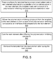
The NIL process also includes diffusing 520 the polymerization inhibiting compound from the template to the resin element to form a layer of the polymerization inhibiting compound at the interface of the template and the resin element. The diffusion is performed by holding the template together with the resin from five seconds to two minutes. In some embodiments, the diffusion is performed while the template and/or the resin are heated in order to increase the diffusion rate. The layer of the polymerization inhibiting compound formed by the diffusion has a thickness no more than 10 nm.
The NIL process further includes curing 530 the resin element after diffusing the polymerization inhibiting compound. The resin element is cured by being exposed to ultraviolet light. The ML process also includes removing 540 the template from the resin element after curing the resin element. The polymerization inhibiting compound at the interface of the resin element and template prevents adhesive failure during the removing.
Compared with the NIL process in FIG. 3 , the NIL process in FIG. 5 does not have the step to prepare the layer of the polymerization inhibiting compound since the layer is formed by diffusion when the template is pressed onto the resin element. However, the layer of the polymerization inhibiting compound that is deposited to the template in FIG. 3 is better conformed to the template.
The NIL process also includes pressing 720 a surface of a template having a nano-sized pattern onto the surface of the resin element exposed to the air to form the nano-sized structure in the resin element. During and after the pressing, the polymerization inhibiting compound remains at the interface of the template and the resin element.
The NIL process further includes curing 730 the resin element after forming the nano-sized structure in the resin element and removing 740 the template from the resin element after curing the resin element. As discussed above, because the polymerization inhibiting compound inhibits polymerization at the interface of the molded resin element and the template, there is no adhesive failure during the removing.
The NIL process has multiple advantages. One advantage is that there is no additional step to prepare the layer of the polymerization inhibiting compound since the layer is formed during the aging process. Another advantage is that the template and the polymerization inhibiting compound does not have to have orthogonal polymerization chemistries since the polymerization inhibiting compound is formed in the resin element. Thus, there are more materials that can be selected as the polymerization inhibiting compound.
Claims (12)
1. A method for fabricating a nano-sized structure, comprising:
pressing a surface of a template having a nano-sized pattern onto a resin element attached on a substrate to form the nano-sized structure in the resin element, the template made with a mixture of a polymerization inhibiting compound and an elastomeric resin;
diffusing the polymerization inhibiting compound from the template to the resin element to form a layer of the polymerization inhibiting compound at an interface of the template and the resin element;
curing the resin element after diffusing the polymerization inhibiting compound; and
removing the template from the resin element after curing the resin element.
2. The method of claim 1 , wherein the polymerization inhibiting compound includes at least one of the following functional groups: amine, phenol, quinone, nitroso, persistent free radical, or some combination thereof.
3. The method of claim 1 , wherein a ratio of the polymerization inhibiting compound and the elastomeric resin in the template is in a range from 1:99 to 1:9.
4. The method of claim 1 , wherein the layer of the polymerization inhibiting compound has a thickness no more than 10 nanometers.
5. The method of claim 1 , wherein the template is made by free radical polymerization and the resin element is made by cationic polymerization.
6. The method of claim 1 , wherein diffusing inhibiting compound from the template to the resin element is performed by holding the template together with the resin for a period of time from five seconds to two minutes.
7. The method of claim 1 , wherein diffusion of the inhibiting compound from the template to the resin element is performed while the template and resin element are being heated.
8. The method of claim 1 , wherein the template is a soft template.
9. The method of claim 1 , wherein the resin element comprises a fluorine resin.
10. The method of claim 1 , wherein the resin element is coated on the substrate by spin coating.
11. The method of claim 1 , wherein curing the resin element comprises:
exposing the resin element to ultraviolet light.
12. The method of claim 1 , wherein the template is made by cationic polymerization and the resin element is made by free radical polymerization.
Priority Applications (2)
| Application Number | Priority Date | Filing Date | Title |
|---|---|---|---|
| US16/216,809 US10857724B1 (en) | 2018-12-11 | 2018-12-11 | Reducing adhesive failure during nanoimprint lithography demolding |
| US17/083,826 US11173649B1 (en) | 2018-12-11 | 2020-10-29 | Reducing adhesive failure during nanoimprint lithography demolding |
Applications Claiming Priority (1)
| Application Number | Priority Date | Filing Date | Title |
|---|---|---|---|
| US16/216,809 US10857724B1 (en) | 2018-12-11 | 2018-12-11 | Reducing adhesive failure during nanoimprint lithography demolding |
Related Child Applications (1)
| Application Number | Title | Priority Date | Filing Date |
|---|---|---|---|
| US17/083,826 Continuation US11173649B1 (en) | 2018-12-11 | 2020-10-29 | Reducing adhesive failure during nanoimprint lithography demolding |
Publications (1)
| Publication Number | Publication Date |
|---|---|
| US10857724B1 true US10857724B1 (en) | 2020-12-08 |
Family
ID=73653661
Family Applications (2)
| Application Number | Title | Priority Date | Filing Date |
|---|---|---|---|
| US16/216,809 Active 2039-04-02 US10857724B1 (en) | 2018-12-11 | 2018-12-11 | Reducing adhesive failure during nanoimprint lithography demolding |
| US17/083,826 Active US11173649B1 (en) | 2018-12-11 | 2020-10-29 | Reducing adhesive failure during nanoimprint lithography demolding |
Family Applications After (1)
| Application Number | Title | Priority Date | Filing Date |
|---|---|---|---|
| US17/083,826 Active US11173649B1 (en) | 2018-12-11 | 2020-10-29 | Reducing adhesive failure during nanoimprint lithography demolding |
Country Status (1)
| Country | Link |
|---|---|
| US (2) | US10857724B1 (en) |
Cited By (2)
| Publication number | Priority date | Publication date | Assignee | Title |
|---|---|---|---|---|
| US11262650B1 (en) * | 2018-12-11 | 2022-03-01 | Facebook Technologies, Llc | Reducing adhesive failure during nanoimprint lithography demolding |
| US11294278B1 (en) | 2018-12-11 | 2022-04-05 | Facebook Technologies, Llc | Reducing adhesive failure during nanoimprint lithography demolding |
Citations (1)
| Publication number | Priority date | Publication date | Assignee | Title |
|---|---|---|---|---|
| US20130281713A1 (en) * | 2010-02-19 | 2013-10-24 | Board Of Regents The University Of Texas System | Branched siloxanes and methods for synthesis |
Family Cites Families (30)
| Publication number | Priority date | Publication date | Assignee | Title |
|---|---|---|---|---|
| US4090997A (en) | 1976-03-05 | 1978-05-23 | Felt Products Mfg. Co. | High-strength anaerobic sealant composition and method of preparation |
| US4535041A (en) | 1984-08-20 | 1985-08-13 | Polaroid Corporation | Stabilization of holograms |
| US5079131A (en) | 1988-08-29 | 1992-01-07 | Shipley Company Inc. | Method of forming positive images through organometallic treatment of negative acid hardening cross-linked photoresist formulations |
| JPH0792605B2 (en) | 1989-11-02 | 1995-10-09 | 三菱電機株式会社 | Resist pattern formation method |
| JPH03248414A (en) | 1990-02-26 | 1991-11-06 | Mitsubishi Electric Corp | Formation of fine pattern using selective surface reaction |
| JPH05150459A (en) | 1991-05-24 | 1993-06-18 | Nippon Paint Co Ltd | Formation of resist pattern |
| US5407787A (en) | 1993-04-14 | 1995-04-18 | The United States Of America As Represented By The Secretary Of The Navy | Process to fabricate thick coplanar microwave electrode structures |
| KR0174316B1 (en) | 1994-07-05 | 1999-04-01 | 모리시다 요이치 | Method of forming micropatterns |
| JPH1073713A (en) | 1996-08-30 | 1998-03-17 | Hoechst Ind Kk | Photosensitive resin composition for color filter |
| GB9717407D0 (en) | 1997-08-18 | 1997-10-22 | Isis Innovation | Photonic crystal materials and a method of preparation thereof |
| WO1999052018A1 (en) | 1998-04-07 | 1999-10-14 | Euv Limited Liability Corporation | Thin layer imaging process for microlithography using radiation at strongly attenuated wavelengths |
| JP3120402B2 (en) | 1998-09-03 | 2000-12-25 | インターナショナル・ビジネス・マシーンズ・コーポレ−ション | Photoresist composition containing passivated aromatic amine compound |
| US6379869B1 (en) | 1999-03-31 | 2002-04-30 | Infineon Technologies Ag | Method of improving the etch resistance of chemically amplified photoresists by introducing silicon after patterning |
| US7008757B2 (en) | 2002-12-17 | 2006-03-07 | Lucent Technologies Inc. | Patterned structures of high refractive index materials |
| CN100392444C (en) | 2003-12-05 | 2008-06-04 | 3M创新有限公司 | Method for producing photon crystal and controllable defect therein |
| DE102004061323A1 (en) | 2004-12-20 | 2006-06-22 | Epg (Engineered Nanoproducts Germany)Gmbh | Optical component of an inorganic-organic hybrid material for the production of refractive index gradient layers with high lateral resolution and method for their preparation |
| US7566525B2 (en) | 2005-06-14 | 2009-07-28 | Taiwan Semiconductor Manufacturing Co., Ltd. | Method for forming an anti-etching shielding layer of resist patterns in semiconductor fabrication |
| KR100790899B1 (en) | 2006-12-01 | 2008-01-03 | 삼성전자주식회사 | Template with alignment mark and manufacturing method for the same |
| JP4893433B2 (en) | 2007-04-10 | 2012-03-07 | Tdk株式会社 | Volume hologram recording material and volume hologram recording medium |
| US20100109195A1 (en) | 2008-11-05 | 2010-05-06 | Molecular Imprints, Inc. | Release agent partition control in imprint lithography |
| WO2012133597A1 (en) | 2011-03-30 | 2012-10-04 | Jsr株式会社 | Multilayer resist process pattern forming method and inorganic film forming composition for multilayer resist process |
| US20130108956A1 (en) | 2011-11-01 | 2013-05-02 | Az Electronic Materials Usa Corp. | Nanocomposite positive photosensitive composition and use thereof |
| JP5827180B2 (en) | 2012-06-18 | 2015-12-02 | 富士フイルム株式会社 | Imprint curable composition and substrate adhesion composition, and semiconductor device using the same |
| WO2014031432A1 (en) | 2012-08-22 | 2014-02-27 | Board Of Regents, The University Of Texas System | Method for creating topographical patterns in polymers via surface energy patterned films and the marangoni effect |
| US20140235727A1 (en) | 2013-02-20 | 2014-08-21 | First Water Limited | Antimicrobial hydrogel polymers |
| JP6119544B2 (en) | 2013-10-04 | 2017-04-26 | 信越化学工業株式会社 | Resist material and pattern forming method using the same |
| KR102352289B1 (en) | 2014-04-17 | 2022-01-19 | 삼성디스플레이 주식회사 | Photoresist composition and method of fabricating display substrate using the same |
| US10509313B2 (en) | 2016-06-28 | 2019-12-17 | Canon Kabushiki Kaisha | Imprint resist with fluorinated photoinitiator and substrate pretreatment for reducing fill time in nanoimprint lithography |
| WO2018236355A1 (en) | 2017-06-20 | 2018-12-27 | Intel Corporation | Passivating silicide-based approaches for conductive via fabrication and structures resulting therefrom |
| WO2019044505A1 (en) | 2017-08-31 | 2019-03-07 | 富士フイルム株式会社 | Resin composition, film, near-infrared cut filter, infrared-transmitting filter, solid imaging element, image display device, infrared sensor, and camera module |
-
2018
- 2018-12-11 US US16/216,809 patent/US10857724B1/en active Active
-
2020
- 2020-10-29 US US17/083,826 patent/US11173649B1/en active Active
Patent Citations (1)
| Publication number | Priority date | Publication date | Assignee | Title |
|---|---|---|---|---|
| US20130281713A1 (en) * | 2010-02-19 | 2013-10-24 | Board Of Regents The University Of Texas System | Branched siloxanes and methods for synthesis |
Cited By (2)
| Publication number | Priority date | Publication date | Assignee | Title |
|---|---|---|---|---|
| US11262650B1 (en) * | 2018-12-11 | 2022-03-01 | Facebook Technologies, Llc | Reducing adhesive failure during nanoimprint lithography demolding |
| US11294278B1 (en) | 2018-12-11 | 2022-04-05 | Facebook Technologies, Llc | Reducing adhesive failure during nanoimprint lithography demolding |
Also Published As
| Publication number | Publication date |
|---|---|
| US11173649B1 (en) | 2021-11-16 |
Similar Documents
| Publication | Publication Date | Title |
|---|---|---|
| US11173649B1 (en) | Reducing adhesive failure during nanoimprint lithography demolding | |
| KR102307788B1 (en) | Nanostructures for oled devices | |
| JP5753132B2 (en) | Materials for imprint lithography | |
| US7858010B2 (en) | Soft template with alignment mark | |
| US8616873B2 (en) | Micro-conformal templates for nanoimprint lithography | |
| US7094304B2 (en) | Method for selective area stamping of optical elements on a substrate | |
| KR101020634B1 (en) | Manufacturing method of lens having nanopattern | |
| EP1497695A2 (en) | Nanoimprint resist | |
| KR101691157B1 (en) | Method of manufacturing stamp for nanoimprint | |
| EP3237971B1 (en) | Patterned stamp manufacturing method, patterned stamp and imprinting method | |
| CN110429100B (en) | Display panel and preparation method and application thereof | |
| US11453232B2 (en) | Patterned stamp manufacturing method, patterned stamp imprinting method and imprinted article | |
| KR20090003601A (en) | Flexible photomask and method for manufacturing the same | |
| TW505976B (en) | Method for forming micro-pattern of semiconductor device | |
| US11262650B1 (en) | Reducing adhesive failure during nanoimprint lithography demolding | |
| US11294278B1 (en) | Reducing adhesive failure during nanoimprint lithography demolding | |
| KR101179063B1 (en) | Materials for imprint lithography | |
| KR101655035B1 (en) | Photomask and method of manufacturing photomask | |
| US20100143849A1 (en) | Semiconductor device manufacturing method | |
| KR101575879B1 (en) | Patterning method using reversal imprint process | |
| KR20120020012A (en) | Organic-inorganic hybrid material and stamp for nanoimprint manufactured from the same | |
| JP4889316B2 (en) | A manufacturing method of a three-dimensional structure, a three-dimensional structure, an optical element, a stencil mask, a manufacturing method of a finely processed product, and a manufacturing method of a fine pattern molded product. | |
| US8975189B2 (en) | Method of forming fine patterns | |
| Youn et al. | Microstructuring of 45-µm-Deep Dual Damascene Openings in SU-8/Si by UV-Assisted Thermal Imprinting with Opaque Mold | |
| KR100734664B1 (en) | Method for forming a minute pattern using a langmuir-blodegett way |
Legal Events
| Date | Code | Title | Description |
|---|---|---|---|
| FEPP | Fee payment procedure |
Free format text: ENTITY STATUS SET TO UNDISCOUNTED (ORIGINAL EVENT CODE: BIG.); ENTITY STATUS OF PATENT OWNER: LARGE ENTITY |
|
| STCF | Information on status: patent grant |
Free format text: PATENTED CASE |