US10856414B2 - System and method for minimizing connector pad open-circuit stubs - Google Patents
System and method for minimizing connector pad open-circuit stubs Download PDFInfo
- Publication number
- US10856414B2 US10856414B2 US15/918,491 US201815918491A US10856414B2 US 10856414 B2 US10856414 B2 US 10856414B2 US 201815918491 A US201815918491 A US 201815918491A US 10856414 B2 US10856414 B2 US 10856414B2
- Authority
- US
- United States
- Prior art keywords
- connector pad
- connector
- island
- length
- base
- Prior art date
- Legal status (The legal status is an assumption and is not a legal conclusion. Google has not performed a legal analysis and makes no representation as to the accuracy of the status listed.)
- Active
Links
Images


Classifications
-
- H—ELECTRICITY
- H05—ELECTRIC TECHNIQUES NOT OTHERWISE PROVIDED FOR
- H05K—PRINTED CIRCUITS; CASINGS OR CONSTRUCTIONAL DETAILS OF ELECTRIC APPARATUS; MANUFACTURE OF ASSEMBLAGES OF ELECTRICAL COMPONENTS
- H05K1/00—Printed circuits
- H05K1/02—Details
- H05K1/11—Printed elements for providing electric connections to or between printed circuits
- H05K1/111—Pads for surface mounting, e.g. lay-out
-
- H—ELECTRICITY
- H05—ELECTRIC TECHNIQUES NOT OTHERWISE PROVIDED FOR
- H05K—PRINTED CIRCUITS; CASINGS OR CONSTRUCTIONAL DETAILS OF ELECTRIC APPARATUS; MANUFACTURE OF ASSEMBLAGES OF ELECTRICAL COMPONENTS
- H05K1/00—Printed circuits
- H05K1/02—Details
- H05K1/0213—Electrical arrangements not otherwise provided for
- H05K1/0237—High frequency adaptations
- H05K1/024—Dielectric details, e.g. changing the dielectric material around a transmission line
-
- H—ELECTRICITY
- H05—ELECTRIC TECHNIQUES NOT OTHERWISE PROVIDED FOR
- H05K—PRINTED CIRCUITS; CASINGS OR CONSTRUCTIONAL DETAILS OF ELECTRIC APPARATUS; MANUFACTURE OF ASSEMBLAGES OF ELECTRICAL COMPONENTS
- H05K1/00—Printed circuits
- H05K1/02—Details
- H05K1/0213—Electrical arrangements not otherwise provided for
- H05K1/0237—High frequency adaptations
- H05K1/0243—Printed circuits associated with mounted high frequency components
-
- H—ELECTRICITY
- H05—ELECTRIC TECHNIQUES NOT OTHERWISE PROVIDED FOR
- H05K—PRINTED CIRCUITS; CASINGS OR CONSTRUCTIONAL DETAILS OF ELECTRIC APPARATUS; MANUFACTURE OF ASSEMBLAGES OF ELECTRICAL COMPONENTS
- H05K1/00—Printed circuits
- H05K1/18—Printed circuits structurally associated with non-printed electric components
- H05K1/181—Printed circuits structurally associated with non-printed electric components associated with surface mounted components
-
- H—ELECTRICITY
- H05—ELECTRIC TECHNIQUES NOT OTHERWISE PROVIDED FOR
- H05K—PRINTED CIRCUITS; CASINGS OR CONSTRUCTIONAL DETAILS OF ELECTRIC APPARATUS; MANUFACTURE OF ASSEMBLAGES OF ELECTRICAL COMPONENTS
- H05K3/00—Apparatus or processes for manufacturing printed circuits
- H05K3/40—Forming printed elements for providing electric connections to or between printed circuits
- H05K3/4007—Surface contacts, e.g. bumps
-
- H—ELECTRICITY
- H05—ELECTRIC TECHNIQUES NOT OTHERWISE PROVIDED FOR
- H05K—PRINTED CIRCUITS; CASINGS OR CONSTRUCTIONAL DETAILS OF ELECTRIC APPARATUS; MANUFACTURE OF ASSEMBLAGES OF ELECTRICAL COMPONENTS
- H05K2201/00—Indexing scheme relating to printed circuits covered by H05K1/00
- H05K2201/09—Shape and layout
- H05K2201/09209—Shape and layout details of conductors
- H05K2201/09654—Shape and layout details of conductors covering at least two types of conductors provided for in H05K2201/09218 - H05K2201/095
- H05K2201/09781—Dummy conductors, i.e. not used for normal transport of current; Dummy electrodes of components
-
- H—ELECTRICITY
- H05—ELECTRIC TECHNIQUES NOT OTHERWISE PROVIDED FOR
- H05K—PRINTED CIRCUITS; CASINGS OR CONSTRUCTIONAL DETAILS OF ELECTRIC APPARATUS; MANUFACTURE OF ASSEMBLAGES OF ELECTRICAL COMPONENTS
- H05K2201/00—Indexing scheme relating to printed circuits covered by H05K1/00
- H05K2201/10—Details of components or other objects attached to or integrated in a printed circuit board
- H05K2201/10613—Details of electrical connections of non-printed components, e.g. special leads
- H05K2201/10621—Components characterised by their electrical contacts
- H05K2201/10628—Leaded surface mounted device
-
- H—ELECTRICITY
- H05—ELECTRIC TECHNIQUES NOT OTHERWISE PROVIDED FOR
- H05K—PRINTED CIRCUITS; CASINGS OR CONSTRUCTIONAL DETAILS OF ELECTRIC APPARATUS; MANUFACTURE OF ASSEMBLAGES OF ELECTRICAL COMPONENTS
- H05K2201/00—Indexing scheme relating to printed circuits covered by H05K1/00
- H05K2201/10—Details of components or other objects attached to or integrated in a printed circuit board
- H05K2201/10613—Details of electrical connections of non-printed components, e.g. special leads
- H05K2201/10742—Details of leads
- H05K2201/1075—Shape details
- H05K2201/10757—Bent leads
-
- H—ELECTRICITY
- H05—ELECTRIC TECHNIQUES NOT OTHERWISE PROVIDED FOR
- H05K—PRINTED CIRCUITS; CASINGS OR CONSTRUCTIONAL DETAILS OF ELECTRIC APPARATUS; MANUFACTURE OF ASSEMBLAGES OF ELECTRICAL COMPONENTS
- H05K3/00—Apparatus or processes for manufacturing printed circuits
- H05K3/30—Assembling printed circuits with electric components, e.g. with resistor
- H05K3/32—Assembling printed circuits with electric components, e.g. with resistor electrically connecting electric components or wires to printed circuits
- H05K3/34—Assembling printed circuits with electric components, e.g. with resistor electrically connecting electric components or wires to printed circuits by soldering
- H05K3/341—Surface mounted components
- H05K3/3421—Leaded components
-
- Y—GENERAL TAGGING OF NEW TECHNOLOGICAL DEVELOPMENTS; GENERAL TAGGING OF CROSS-SECTIONAL TECHNOLOGIES SPANNING OVER SEVERAL SECTIONS OF THE IPC; TECHNICAL SUBJECTS COVERED BY FORMER USPC CROSS-REFERENCE ART COLLECTIONS [XRACs] AND DIGESTS
- Y02—TECHNOLOGIES OR APPLICATIONS FOR MITIGATION OR ADAPTATION AGAINST CLIMATE CHANGE
- Y02P—CLIMATE CHANGE MITIGATION TECHNOLOGIES IN THE PRODUCTION OR PROCESSING OF GOODS
- Y02P70/00—Climate change mitigation technologies in the production process for final industrial or consumer products
- Y02P70/50—Manufacturing or production processes characterised by the final manufactured product
Definitions
- This disclosure generally relates to information handling systems, and more particularly relates to minimizing connector pad open-circuit stubs.
- An information handling system generally processes, compiles, stores, and/or communicates information or data for business, personal, or other purposes. Because technology and information handling needs and requirements may vary between different applications, information handling systems may also vary regarding what information is handled, how the information is handled, how much information is processed, stored, or communicated, and how quickly and efficiently the information may be processed, stored, or communicated. The variations in information handling systems allow for information handling systems to be general or configured for a specific user or specific use such as financial transaction processing, reservations, enterprise data storage, or global communications. In addition, information handling systems may include a variety of hardware and software resources that may be configured to process, store, and communicate information and may include one or more computer systems, data storage systems, and networking systems.
- a printed circuit board may include a circuit trace and a connector pad.
- the connector pad can provide electrical and mechanical mounting of a connector lead of a surface mount device.
- the connector pad can also provide a circuit path between the surface mount device and the circuit trace.
- the connector pad may include 1) a connector pad base electrically coupled to the circuit trace, and 2) a first connector pad island electrically isolated from the connector pad base.
- the connector pad base may have a length that is substantially equal to a length of a contact portion of the connector lead.
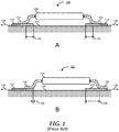
- FIG. 1 is a schematic of a surface mount device mounted to a printed circuit board (PCB) in accordance with the prior art
- FIG. 2 is a top view of a connector pad of the PCB of FIG. 1 ;
- FIG. 3 is a signal trace of a signal eye diagram for a data channel of a serial data interface of the PCB of FIG. 1 ;
- FIG. 4 is a top view of a connector pad according to an embodiment of the present disclosure.
- FIG. 5 is a schematic view of a surface mount device mounted to a PCB using the connector pad of FIG. 4 ;
- FIG. 6 is a signal trace of a signal eye diagram for a data channel of a serial data interface of the PCB of FIG. 5 ;
- FIG. 7 is a block diagram illustrating a generalized information handling system according to an embodiment of the present disclosure.
- FIG. 1 illustrates a surface mount device (SMD) 120 mounted to a printed circuit board (PCB) 110 , as is known in the art.
- SMD 120 includes connector leads 122 and a device 124 .
- Device 124 represents a wide variety of electrical and electronic components that are available in surface mount packages as are known in the art.
- device 124 can represent a discrete device or group of passive devices, such as capacitors, resistors, inductors, discrete transistors and the like that can be packaged as surface mount devices.
- device 124 can represent an integrated circuit device that can be packaged as a surface mount device.
- Connector leads 122 operate to provide a mechanical attachment to PCB 110 .
- Connector leads 122 are placed such that a contact portion of the connector leads are place atop connector pads 112 that are provided on the surface of the PCB, and then being soldered to the connector pads, firmly attaching SMD 120 to the PCB.
- Connector leads 122 also operate to provide electrical connection between PCB 110 and device 124 .
- connector pads 112 are connected to various circuit traces of PCB 110
- connector leads 122 are connected to device 124 via their soldered contact portions to provide the various circuit paths for performing the processing tasks associated with the PCB.
- connector pads 112 and connector leads 122 are shown as providing respective circuit paths 130 .
- Connector pads 112 are deliberately sized larger than the actual size needed to make the mechanical and electrical connections necessary for secure attachment and signal transmission.
- SMD 120 is optimally placed upon PCB 110 , with connector leads 122 centered on connector pads 112 .
- SMD 120 still retains sufficient mechanical and electrical contact to connector pads 112 via connector leads 122 as to retain mechanical and electrical contact between PCB 110 and device 124 .
- circuits associated with circuit paths 130 are high speed circuits
- the signals carried by the circuit paths may operate at very high frequencies.
- any length of connector pads 112 that is beyond the point of contact between the connector pads and connector leads 122 are not actually utilized in carrying the electrical signals of circuit paths 130 , but instead act as open-circuit stubs that resonate at a characteristic frequency that is determined by the length of the stub.
- the excess length of circuit pads 112 provide for similar lengths of open-circuit stubs 132 .
- SMD 120 is placed as shown in the bottom illustration B of FIG.
- one side will exhibit a short open-circuit stub 134 and the other side will exhibit a long open-circuit stub 136 .
- SMD 120 is deemed to be correctly placed on PCB 110 . That is, both placements are to be considered as being within the normal process variation for PCB manufacturing processes, and illustration B should not be considered misaligned.
- the resonate frequency of an open-circuit stub can be expressed as:
- f res C 0 4 ⁇ ⁇ eff ⁇ L stub Equation ⁇ ⁇ 1
- f res is the resonate frequency in mega-Hertz (MHz)
- co is the speed of a wave in free space (3.0 ⁇ 10 8 meters per second (m/s)
- ⁇ eff is the effective dielectric constant of the PCB
- L stub is the length of the open-circuit stub.
- the dielectric constant of free air ⁇ r-air is equal to 1
- PCB is typically equal to 4.
- FIG. 2 is a top view of connector pad 112 with an associated circuit trace 114 on PCB 110 .
- Connector pad 112 has an overall length of 4 millimeters (mm), or 157 mils.
- open-circuit stubs 132 are typically around 70 mils (0.76 mm), but when the SMD is placed as shown in illustration B, open-circuit stub 134 can be as short as 10 mils (0.25 mm), and open-circuit stub 136 can be as long as 50 mils (1.27 mm).
- the resonate frequency can vary between 37.3-186.7 GHz. These resonate frequencies are higher than the Nyquist frequency of current and future generation serial data interfaces.
- PCIe gen 4 has a maximum data rate of 16 giga-bits per second (16 G bps) and a Nyquist frequency of 8 GHz
- PCIe gen 5 has a maximum data rate of 72 G bps and a Nyquist frequency of 16 GHz.
- ⁇ eff 2.5
- FIG. 3 illustrates a trace of a signal eye diagram for a data channel of a serial data interface.
- the illustration shows a poor quality signal eye diagram for the data channel that includes an SMD that is attached to a PCB with an open-circuit stub with a longer stub length, such as might be provided by a less than optimally placed SMD, such as for a data channel with a 50 mil stub.
- FIG. 4 is a top view of a connector pad 412 with an associated circuit trace 414 on a PCB 410 according to an embodiment of the present disclosure.
- Connector pad 412 is similar to connector pad 112 , having an overall length of 4 millimeters (mm), or 157 mils. However, connector pad 412 differs from connector pad 112 in that connector pad 412 includes a connector pad base 416 and one or more connector pad islands 418 . Connector pad portion 416 and connector pad islands 418 are electrically isolated from each other.
- the metal trace material of circuit trace 414 is formed continuously with the metal trace material of connector pad base 416 , and each of connector pad islands 418 are formed as separate and isolated metalization on the surface of the PCB.
- connector pad islands 418 are 7-8 mils wide and are spaced 7-8 mils apart.
- length and distance between connector pad islands 418 will be provided based upon the manufacturing tolerances of PCB 410 .
- the dimensions of connector pad islands 418 and the distances there between will be dictated by the ability of solder to be applied to the surface of PCB 410 and to remain soldered to the connector pad islands without forming solder bridges between the connector pad islands.
- FIG. 5 illustrates a surface mount device (SMD) 420 mounted to PCB 410 .
- SMD 420 includes connector leads 422 and a device 424 .
- Device 424 is similar to device 124 .
- Connector leads 422 are similar to connector leads 122 , providing mechanical and electrical attachment to PCB 410 .
- Connector pads 412 (shown in this view by connector pad bases 416 and connector pad islands 418 , and connector leads 422 are shown as providing respective circuit paths 430 .
- Connector pads 412 are deliberately sized larger than the actual size needed to make the mechanical and electrical connections necessary for secure attachment and signal transmission to account for manufacturing process tolerances. Thus, as shown in the top illustration A of FIG.
- SMD 420 is optimally placed upon PCB 410 , with connector leads 422 centered on connector pads 142 . Further, as is shown in the bottom illustration B of FIG. 5 , SMD 420 still retains sufficient mechanical and electrical contact to connector pads 412 via connector leads 422 as to retain mechanical and electrical contact between PCB 410 and device 424 when SMD is placed slightly askew on the PCB.
- connector leads 422 may bridge between connector pad bases 416 and connector pad islands 418 .
- both of connector leads 422 are bridge between their respective connector pad base 416 and a single connector pad island 418 .
- connector lead 422 on the left side bridges between the associated connector pad base 422 and three (3) of connector pad islands 418 . Then, when SMD 420 is soldered to PCB 400 , the solder reflows between connector pad bases 416 and the bridged connector pad islands 418 , making a continuous circuit path for circuit paths 430 .
- the open-circuit stubs 432 that are minimized by the length of a single connector pad island 418 and the spacing between the connector pad islands. For example, in a worst case, where connector pad islands 418 are 8 mils wide, and are spaced 8 mils apart, then open-circuit stub 432 will not exceed 16 mils, and the resonate frequency may be expected to be 149.4 GHz, far beyond the Nyquist frequency of current and future generation serial data interfaces. Note that even when connector lead 422 is located completely atop connector pad base 422 , as shown in the right side of illustration B, the open-circuit stub 434 that is formed at the end of the connector pad base is far shorter than the similarly placed connector lead as depicted in FIG. 1 .
- FIG. 6 is a trace of a signal eye diagram for a data channel of a serial data interface that utilizes connector pad 412 .
- the illustration shows a better quality signal eye diagram for the data channel than for the similar data channel as shown in FIG. 3 .
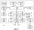
- FIG. 7 illustrates a generalized embodiment of an information handling system 700 similar to information handling system 100 .
- information handling system 700 can be configured to provide the features and to perform the functions of the OPF system as described herein.
- Information handling system 700 can include any instrumentality or aggregate of instrumentalities operable to compute, classify, process, transmit, receive, retrieve, originate, switch, store, display, manifest, detect, record, reproduce, handle, or utilize any form of information, intelligence, or data for business, scientific, control, entertainment, or other purposes.
- information handling system 700 can be a personal computer, a laptop computer, a smart phone, a tablet device or other consumer electronic device, a network server, a network storage device, a switch router or other network communication device, or any other suitable device and may vary in size, shape, performance, functionality, and price.
- information handling system 700 can include processing resources for executing machine-executable code, such as a central processing unit (CPU), a programmable logic array (PLA), an embedded device such as a System-on-a-Chip (SoC), or other control logic hardware.
- Information handling system 700 can also include one or more computer-readable medium for storing machine-executable code, such as software or data.
- Additional components of information handling system 700 can include one or more storage devices that can store machine-executable code, one or more communications ports for communicating with external devices, and various input and output (I/O) devices, such as a keyboard, a mouse, and a video display.
- Information handling system 700 can also include one or more buses operable to transmit information between the various hardware components.
- Information handling system 700 can include devices or modules that embody one or more of the devices or modules described below, and operates to perform one or more of the methods described below.
- Information handling system 700 includes a processors 702 and 704 , a chipset 710 , a memory 720 , a graphics interface 730 , a basic input and output system/universal extensible firmware interface (BIOS/UEFI) module 740 , a disk controller 750 , a hard disk drive (HDD) 754 , an optical disk drive (ODD) 756 , a disk emulator 760 connected to an external solid state drive (SSD) 762 , an input/output (I/O) interface 770 , one or more add-on resources 774 , a trusted platform module (TPM) 776 , a network interface 780 , a management device 790 , and a power supply 795 .
- a processors 702 and 704 includes a processors 702 and 704 , a chipset 710 ,
- Processors 702 and 704 operate together to provide a host environment of information handling system 700 that operates to provide the data processing functionality of the information handling system.
- the host environment operates to execute machine-executable code, including platform BIOS/UEFI code, device firmware, operating system code, applications, programs, and the like, to perform the data processing tasks associated with information handling system 700 .
- processor 702 is connected to chipset 710 via processor interface 706
- processor 704 is connected to the chipset via processor interface 708
- Memory 720 is connected to chipset 710 via a memory bus 722 .
- Graphics interface 730 is connected to chipset 710 via a graphics interface 732 , and provides a video display output 736 to a video display 734 .
- information handling system 700 includes separate memories that are dedicated to each of processors 702 and 704 via separate memory interfaces.
- An example of memory 720 includes random access memory (RAM) such as static RAM (SRAM), dynamic RAM (DRAM), non-volatile RAM (NV-RAM), or the like, read only memory (ROM), another type of memory, or a combination thereof.
- RAM random access memory
- SRAM static RAM
- DRAM dynamic RAM
- NV-RAM non-volatile RAM
- ROM read only memory
- BIOS/UEFI module 740 , disk controller 750 , and I/O interface 770 are connected to chipset 710 via an I/O channel 712 .
- I/O channel 712 includes a Peripheral Component Interconnect (PCI) interface, a PCI-Extended (PCI-X) interface, a high speed PCI-Express (PCIe) interface, another industry standard or proprietary communication interface, or a combination thereof.
- Chipset 710 can also include one or more other I/O interfaces, including an Industry Standard Architecture (ISA) interface, a Small Computer Serial Interface (SCSI) interface, an Inter-Integrated Circuit (I 2 C) interface, a System Packet Interface (SPI), a Universal Serial Bus (USB), another interface, or a combination thereof.
- ISA Industry Standard Architecture
- SCSI Small Computer Serial Interface
- I 2 C Inter-Integrated Circuit
- SPI System Packet Interface
- USB Universal Serial Bus
- BIOS/UEFI module 740 includes BIOS/UEFI code operable to detect resources within information handling system 700 , to provide drivers for the resources, initialize the resources, and access the resources.
- BIOS/UEFI module 740 includes code that operates to detect resources within information handling system 700 , to provide drivers for the resources, to initialize the resources, and to access the resources.
- Disk controller 750 includes a disk interface 752 that connects the disk controller to HDD 754 , to ODD 756 , and to disk emulator 760 .
- An example of disk interface 752 includes an Integrated Drive Electronics (IDE) interface, an Advanced Technology Attachment (ATA) such as a parallel ATA (PATA) interface or a serial ATA (SATA) interface, a SCSI interface, a USB interface, a proprietary interface, or a combination thereof.
- Disk emulator 760 permits SSD 764 to be connected to information handling system 700 via an external interface 762 .
- An example of external interface 762 includes a USB interface, an IEEE 1394 (Firewire) interface, a proprietary interface, or a combination thereof.
- solid-state drive 764 can be disposed within information handling system 700 .
- I/O interface 770 includes a peripheral interface 772 that connects the I/O interface to add-on resource 774 , to TPM 776 , and to network interface 780 .
- Peripheral interface 772 can be the same type of interface as I/O channel 712 , or can be a different type of interface.
- I/O interface 770 extends the capacity of I/O channel 712 when peripheral interface 772 and the I/O channel are of the same type, and the I/O interface translates information from a format suitable to the I/O channel to a format suitable to the peripheral channel 772 when they are of a different type.
- Add-on resource 774 can include a data storage system, an additional graphics interface, a network interface card (NIC), a sound/video processing card, another add-on resource, or a combination thereof.
- Add-on resource 774 can be on a main circuit board, on separate circuit board or add-in card disposed within information handling system 700 , a device that is external to the information handling system, or a combination thereof.
- Network interface 780 represents a NIC disposed within information handling system 700 , on a main circuit board of the information handling system, integrated onto another component such as chipset 710 , in another suitable location, or a combination thereof.
- Network interface device 780 includes network channels 782 and 784 that provide interfaces to devices that are external to information handling system 700 .
- network channels 782 and 784 are of a different type than peripheral channel 772 and network interface 780 translates information from a format suitable to the peripheral channel to a format suitable to external devices.
- An example of network channels 782 and 784 includes InfiniBand channels, Fibre Channel channels, Gigabit Ethernet channels, proprietary channel architectures, or a combination thereof.
- Network channels 782 and 784 can be connected to external network resources (not illustrated).
- the network resource can include another information handling system, a data storage system, another network, a grid management system, another suitable resource, or a combination thereof.
- Management device 790 represents one or more processing devices, such as a dedicated baseboard management controller (BMC) System-on-a-Chip (SoC) device, one or more associated memory devices, one or more network interface devices, a complex programmable logic device (CPLD), and the like, that operate together to provide the management environment for information handling system 700 .
- BMC dedicated baseboard management controller
- SoC System-on-a-Chip
- CPLD complex programmable logic device
- management device 790 is connected to various components of the host environment via various internal communication interfaces, such as a Low Pin Count (LPC) interface, an Inter-Integrated-Circuit (I2C) interface, a PCIe interface, or the like, to provide an out-of-band (OOB) mechanism to retrieve information related to the operation of the host environment, to provide BIOS/UEFI or system firmware updates, to manage non-processing components of information handling system 700 , such as system cooling fans and power supplies.
- Management device 790 can include a network connection to an external management system, and the management device can communicate with the management system to report status information for information handling system 700 , to receive BIOS/UEFI or system firmware updates, or to perform other task for managing and controlling the operation of information handling system 700 .
- Management device 790 can operate off of a separate power plane from the components of the host environment so that the management device receives power to manage information handling system 700 when the information handling system is otherwise shut down.
- An example of management device 790 may include a commercially available BMC product that operates in accordance with an Intelligent Platform Management Initiative (IPMI) specification, such as a Integrated Dell Remote Access Controller (iDRAC), or the like.
- IPMI Intelligent Platform Management Initiative
- iDRAC Integrated Dell Remote Access Controller
- Management device 790 may further include associated memory devices, logic devices, security devices, or the like, as needed or desired.
- Power supply 795 represents one or more devices for power distribution to the components of information handling system 700 .
- power supply 795 can include a main power supply that receives power from an input power source, such as a wall power outlet, a power strip, a battery, or another power source, as needed or desired.
- power source 795 operates to convert the power at a first voltage level from the input power source to one or more power rails that are utilized by the components of information handling system.
- Power supply 795 can also include one or more voltage regulators (VRs) that each receive power from the main power supply and that operate to convert the input voltage to an output voltage that is used by one or more components of information handling system.
- VRs voltage regulators
- a VR can be provided for each of processors 702 and 704 , and another VR can be provided for memory 720 .
- Power supply 795 can be configured to provide a first power plane that provides power to the host environment, and to provide a second power plane that provides power to the management environment.
Landscapes
- Engineering & Computer Science (AREA)
- Microelectronics & Electronic Packaging (AREA)
- Manufacturing & Machinery (AREA)
- Details Of Connecting Devices For Male And Female Coupling (AREA)
Abstract
Description
where fres is the resonate frequency in mega-Hertz (MHz), co is the speed of a wave in free space (3.0×10⁸ meters per second (m/s)), εeff is the effective dielectric constant of the PCB, and Lstub is the length of the open-circuit stub. Thus it will be understood that a longer stub will resonate (i.e., radiate signal energy) at a lower resonate frequency, and a shorter stub will resonate at a higher resonate frequency. In a typical PCB such as
| TABLE 1 |
| Resonate Frequency vs. Stub Length |
| εeff = 4 | εeff = 2.5 | εeff = 2 | |||
| Lstub (mils) | fres (GHZ) | fres (GHZ) | fres (GHZ) | ||
| 10 | 147.6 | 186.7 | 208.8 | ||
| 20 | 73.8 | 93.4 | 104.4 | ||
| 30 | 49.2 | 62.2 | 69.6 | ||
| 40 | 36.9 | 46.7 | 52.2 | ||
| 50 | 29.5 | 37.3 | 41.8 | ||
| 60 | 24.6 | 31.1 | 34.8 | ||
| 70 | 21.1 | 26.7 | 29.8 | ||
| 80 | 18.5 | 23.3 | 26.1 | ||
| 90 | 16.4 | 20.7 | 23.2 | ||
| 100 | 14.8 | 18.7 | 20.9 | ||
Claims (20)
Priority Applications (1)
| Application Number | Priority Date | Filing Date | Title |
|---|---|---|---|
| US15/918,491 US10856414B2 (en) | 2018-03-12 | 2018-03-12 | System and method for minimizing connector pad open-circuit stubs |
Applications Claiming Priority (1)
| Application Number | Priority Date | Filing Date | Title |
|---|---|---|---|
| US15/918,491 US10856414B2 (en) | 2018-03-12 | 2018-03-12 | System and method for minimizing connector pad open-circuit stubs |
Publications (2)
| Publication Number | Publication Date |
|---|---|
| US20190281698A1 US20190281698A1 (en) | 2019-09-12 |
| US10856414B2 true US10856414B2 (en) | 2020-12-01 |
Family
ID=67842331
Family Applications (1)
| Application Number | Title | Priority Date | Filing Date |
|---|---|---|---|
| US15/918,491 Active US10856414B2 (en) | 2018-03-12 | 2018-03-12 | System and method for minimizing connector pad open-circuit stubs |
Country Status (1)
| Country | Link |
|---|---|
| US (1) | US10856414B2 (en) |
Families Citing this family (1)
| Publication number | Priority date | Publication date | Assignee | Title |
|---|---|---|---|---|
| CN113766730A (en) * | 2021-07-29 | 2021-12-07 | 苏州浪潮智能科技有限公司 | Connector PCB and differential signal non-stub fan-out wiring structure thereof |
Citations (10)
| Publication number | Priority date | Publication date | Assignee | Title |
|---|---|---|---|---|
| US20050167850A1 (en) * | 1995-12-19 | 2005-08-04 | Moden Walter L. | Flip-chip adaptor package for bare die |
| US7155821B1 (en) | 2004-06-30 | 2007-01-02 | Emc Corporation | Techniques for manufacturing a circuit board having a countersunk via |
| US20090086431A1 (en) * | 2007-09-27 | 2009-04-02 | Sanyo Electric Co., Ltd. | Circuit device, circuit module, and outdoor unit |
| US20100064180A1 (en) | 2008-09-10 | 2010-03-11 | Dell Products, Lp | System and method for stub tuning in an information handling system |
| US20100314751A1 (en) * | 2009-06-14 | 2010-12-16 | Terepac | Processes and structures for IC fabrication |
| US8118611B2 (en) | 2008-10-31 | 2012-02-21 | Myoungsoo Jeon | PCB bridge connector for connecting PCB devices |
| US20130102187A1 (en) | 2011-10-19 | 2013-04-25 | Winchester Electronics Corporation | Closed Entry Din Jack and Connector with PCB Board Lock |
| US20140063767A1 (en) * | 2011-09-30 | 2014-03-06 | Sanyo Electric Co., Ltd. | Circuit device |
| US20160323995A1 (en) | 2013-12-27 | 2016-11-03 | Zte Corporation | Pcb processing method and pcb |
| US20170301653A1 (en) * | 2016-04-18 | 2017-10-19 | Skyworks Solutions, Inc. | Radio frequency system-in-package with stacked clocking crystal |
-
2018
- 2018-03-12 US US15/918,491 patent/US10856414B2/en active Active
Patent Citations (10)
| Publication number | Priority date | Publication date | Assignee | Title |
|---|---|---|---|---|
| US20050167850A1 (en) * | 1995-12-19 | 2005-08-04 | Moden Walter L. | Flip-chip adaptor package for bare die |
| US7155821B1 (en) | 2004-06-30 | 2007-01-02 | Emc Corporation | Techniques for manufacturing a circuit board having a countersunk via |
| US20090086431A1 (en) * | 2007-09-27 | 2009-04-02 | Sanyo Electric Co., Ltd. | Circuit device, circuit module, and outdoor unit |
| US20100064180A1 (en) | 2008-09-10 | 2010-03-11 | Dell Products, Lp | System and method for stub tuning in an information handling system |
| US8118611B2 (en) | 2008-10-31 | 2012-02-21 | Myoungsoo Jeon | PCB bridge connector for connecting PCB devices |
| US20100314751A1 (en) * | 2009-06-14 | 2010-12-16 | Terepac | Processes and structures for IC fabrication |
| US20140063767A1 (en) * | 2011-09-30 | 2014-03-06 | Sanyo Electric Co., Ltd. | Circuit device |
| US20130102187A1 (en) | 2011-10-19 | 2013-04-25 | Winchester Electronics Corporation | Closed Entry Din Jack and Connector with PCB Board Lock |
| US20160323995A1 (en) | 2013-12-27 | 2016-11-03 | Zte Corporation | Pcb processing method and pcb |
| US20170301653A1 (en) * | 2016-04-18 | 2017-10-19 | Skyworks Solutions, Inc. | Radio frequency system-in-package with stacked clocking crystal |
Also Published As
| Publication number | Publication date |
|---|---|
| US20190281698A1 (en) | 2019-09-12 |
Similar Documents
| Publication | Publication Date | Title |
|---|---|---|
| US10856441B1 (en) | System and method for bi-side heating vapor chamber structure in an information handling system | |
| US11710915B2 (en) | System and method for stacking compression dual in-line memory module scalability | |
| US7083423B1 (en) | Method and apparatus for mounting a card connector | |
| US10856414B2 (en) | System and method for minimizing connector pad open-circuit stubs | |
| US11321009B2 (en) | System and method for compression dual in-line memory module scalability | |
| US20220344309A1 (en) | System and method for stacking compression attached memory modules | |
| US11074952B1 (en) | System and method for compression Dual In-Line Memory Module reversibility | |
| US20230030534A1 (en) | Guard trace ground via optimization for high-speed signaling | |
| US11178751B2 (en) | Printed circuit board having vias arranged for high speed serial differential pair data links | |
| US11706869B2 (en) | Crosstalk suppression microstrip line | |
| US11683887B2 (en) | Add-in card connector edge finger optimization for high-speed signaling | |
| US20230030359A1 (en) | Staggered press-fit fish-eye connector | |
| US11757220B2 (en) | Paddle card for crosstalk cancellation in high-speed signaling | |
| US11963289B2 (en) | PCB for heatsink based power delivery | |
| US11924959B2 (en) | Heatsink based power delivery for CPUs | |
| US11837522B2 (en) | Ball grid array package design | |
| US20230337360A1 (en) | Cpu for heatsink based power delivery | |
| US20220350753A1 (en) | System and method for providing compression attached memory module offset stacking | |
| US20230335952A1 (en) | Factory configurable connector impedance | |
| US20220335981A1 (en) | System and method for providing compression attached memory module compression connectors | |
| US20230345629A1 (en) | Pcb stiffening structure to prevent warping | |
| US11439001B2 (en) | System and method for heat removal using a thermal potting solution in an information handling system | |
| US20240098886A1 (en) | Strip line delay matching using printed dielectric material | |
| US20240030635A1 (en) | Method for pre-assembly of compression attached memory modules | |
| US11991819B2 (en) | Microstrip delay matching using printed dielectric material |
Legal Events
| Date | Code | Title | Description |
|---|---|---|---|
| FEPP | Fee payment procedure |
Free format text: ENTITY STATUS SET TO UNDISCOUNTED (ORIGINAL EVENT CODE: BIG.); ENTITY STATUS OF PATENT OWNER: LARGE ENTITY |
|
| AS | Assignment |
Owner name: THE BANK OF NEW YORK MELLON TRUST COMPANY, N.A., A Free format text: PATENT SECURITY AGREEMENT (NOTES);ASSIGNORS:DELL PRODUCTS L.P.;EMC CORPORATION;EMC IP HOLDING COMPANY LLC;REEL/FRAME:046366/0014 Effective date: 20180529 Owner name: CREDIT SUISSE AG, CAYMAN ISLANDS BRANCH, AS COLLAT Free format text: PATENT SECURITY AGREEMENT (CREDIT);ASSIGNORS:DELL PRODUCTS L.P.;EMC CORPORATION;EMC IP HOLDING COMPANY LLC;REEL/FRAME:046286/0653 Effective date: 20180529 Owner name: CREDIT SUISSE AG, CAYMAN ISLANDS BRANCH, AS COLLATERAL AGENT, NORTH CAROLINA Free format text: PATENT SECURITY AGREEMENT (CREDIT);ASSIGNORS:DELL PRODUCTS L.P.;EMC CORPORATION;EMC IP HOLDING COMPANY LLC;REEL/FRAME:046286/0653 Effective date: 20180529 Owner name: THE BANK OF NEW YORK MELLON TRUST COMPANY, N.A., AS COLLATERAL AGENT, TEXAS Free format text: PATENT SECURITY AGREEMENT (NOTES);ASSIGNORS:DELL PRODUCTS L.P.;EMC CORPORATION;EMC IP HOLDING COMPANY LLC;REEL/FRAME:046366/0014 Effective date: 20180529 |
|
| AS | Assignment |
Owner name: THE BANK OF NEW YORK MELLON TRUST COMPANY, N.A., T Free format text: SECURITY AGREEMENT;ASSIGNORS:CREDANT TECHNOLOGIES, INC.;DELL INTERNATIONAL L.L.C.;DELL MARKETING L.P.;AND OTHERS;REEL/FRAME:049452/0223 Effective date: 20190320 Owner name: THE BANK OF NEW YORK MELLON TRUST COMPANY, N.A., TEXAS Free format text: SECURITY AGREEMENT;ASSIGNORS:CREDANT TECHNOLOGIES, INC.;DELL INTERNATIONAL L.L.C.;DELL MARKETING L.P.;AND OTHERS;REEL/FRAME:049452/0223 Effective date: 20190320 |
|
| AS | Assignment |
Owner name: DELL PRODUCTS, LP, TEXAS Free format text: ASSIGNMENT OF ASSIGNORS INTEREST;ASSIGNORS:LIAO, CHUN-LIN;CHEN, CHING-HUEI;MUTNURY, BHYRAV M.;REEL/FRAME:048994/0855 Effective date: 20180309 |
|
| STPP | Information on status: patent application and granting procedure in general |
Free format text: RESPONSE TO NON-FINAL OFFICE ACTION ENTERED AND FORWARDED TO EXAMINER |
|
| STPP | Information on status: patent application and granting procedure in general |
Free format text: NON FINAL ACTION MAILED |
|
| STPP | Information on status: patent application and granting procedure in general |
Free format text: RESPONSE TO NON-FINAL OFFICE ACTION ENTERED AND FORWARDED TO EXAMINER |
|
| STPP | Information on status: patent application and granting procedure in general |
Free format text: FINAL REJECTION MAILED |
|
| AS | Assignment |
Owner name: THE BANK OF NEW YORK MELLON TRUST COMPANY, N.A., TEXAS Free format text: SECURITY AGREEMENT;ASSIGNORS:CREDANT TECHNOLOGIES INC.;DELL INTERNATIONAL L.L.C.;DELL MARKETING L.P.;AND OTHERS;REEL/FRAME:053546/0001 Effective date: 20200409 |
|
| STPP | Information on status: patent application and granting procedure in general |
Free format text: ADVISORY ACTION MAILED |
|
| STPP | Information on status: patent application and granting procedure in general |
Free format text: NOTICE OF ALLOWANCE MAILED -- APPLICATION RECEIVED IN OFFICE OF PUBLICATIONS |
|
| STPP | Information on status: patent application and granting procedure in general |
Free format text: PUBLICATIONS -- ISSUE FEE PAYMENT RECEIVED |
|
| STCF | Information on status: patent grant |
Free format text: PATENTED CASE |
|
| AS | Assignment |
Owner name: EMC IP HOLDING COMPANY LLC, TEXAS Free format text: RELEASE OF SECURITY INTEREST AT REEL 046286 FRAME 0653;ASSIGNOR:CREDIT SUISSE AG, CAYMAN ISLANDS BRANCH;REEL/FRAME:058298/0093 Effective date: 20211101 Owner name: EMC CORPORATION, MASSACHUSETTS Free format text: RELEASE OF SECURITY INTEREST AT REEL 046286 FRAME 0653;ASSIGNOR:CREDIT SUISSE AG, CAYMAN ISLANDS BRANCH;REEL/FRAME:058298/0093 Effective date: 20211101 Owner name: DELL PRODUCTS L.P., TEXAS Free format text: RELEASE OF SECURITY INTEREST AT REEL 046286 FRAME 0653;ASSIGNOR:CREDIT SUISSE AG, CAYMAN ISLANDS BRANCH;REEL/FRAME:058298/0093 Effective date: 20211101 |
|
| AS | Assignment |
Owner name: EMC IP HOLDING COMPANY LLC, TEXAS Free format text: RELEASE OF SECURITY INTEREST IN PATENTS PREVIOUSLY RECORDED AT REEL/FRAME (046366/0014);ASSIGNOR:THE BANK OF NEW YORK MELLON TRUST COMPANY, N.A., AS NOTES COLLATERAL AGENT;REEL/FRAME:060450/0306 Effective date: 20220329 Owner name: EMC CORPORATION, MASSACHUSETTS Free format text: RELEASE OF SECURITY INTEREST IN PATENTS PREVIOUSLY RECORDED AT REEL/FRAME (046366/0014);ASSIGNOR:THE BANK OF NEW YORK MELLON TRUST COMPANY, N.A., AS NOTES COLLATERAL AGENT;REEL/FRAME:060450/0306 Effective date: 20220329 Owner name: DELL PRODUCTS L.P., TEXAS Free format text: RELEASE OF SECURITY INTEREST IN PATENTS PREVIOUSLY RECORDED AT REEL/FRAME (046366/0014);ASSIGNOR:THE BANK OF NEW YORK MELLON TRUST COMPANY, N.A., AS NOTES COLLATERAL AGENT;REEL/FRAME:060450/0306 Effective date: 20220329 |