US10789003B1 - Selective deduplication based on data storage device controller status and media characteristics - Google Patents
Selective deduplication based on data storage device controller status and media characteristics Download PDFInfo
- Publication number
- US10789003B1 US10789003B1 US16/367,900 US201916367900A US10789003B1 US 10789003 B1 US10789003 B1 US 10789003B1 US 201916367900 A US201916367900 A US 201916367900A US 10789003 B1 US10789003 B1 US 10789003B1
- Authority
- US
- United States
- Prior art keywords
- data
- memory
- controller
- fingerprint
- written
- Prior art date
- Legal status (The legal status is an assumption and is not a legal conclusion. Google has not performed a legal analysis and makes no representation as to the accuracy of the status listed.)
- Active
Links
- 238000013500 data storage Methods 0.000 title description 47
- 230000015654 memory Effects 0.000 claims abstract description 219
- 238000000034 method Methods 0.000 claims abstract description 40
- 230000004044 response Effects 0.000 claims abstract description 14
- 238000010801 machine learning Methods 0.000 claims description 3
- 238000012545 processing Methods 0.000 description 24
- 230000006870 function Effects 0.000 description 12
- 238000003491 array Methods 0.000 description 10
- 238000010586 diagram Methods 0.000 description 9
- 238000013528 artificial neural network Methods 0.000 description 8
- 230000008901 benefit Effects 0.000 description 8
- 238000013507 mapping Methods 0.000 description 6
- 230000008569 process Effects 0.000 description 6
- 239000000758 substrate Substances 0.000 description 5
- 238000013461 design Methods 0.000 description 3
- 238000001514 detection method Methods 0.000 description 3
- 238000004088 simulation Methods 0.000 description 3
- 230000003139 buffering effect Effects 0.000 description 2
- 238000005516 engineering process Methods 0.000 description 2
- 238000004519 manufacturing process Methods 0.000 description 2
- 239000007787 solid Substances 0.000 description 2
- 235000008331 Pinus X rigitaeda Nutrition 0.000 description 1
- 235000011613 Pinus brutia Nutrition 0.000 description 1
- 241000018646 Pinus brutia Species 0.000 description 1
- XUIMIQQOPSSXEZ-UHFFFAOYSA-N Silicon Chemical compound [Si] XUIMIQQOPSSXEZ-UHFFFAOYSA-N 0.000 description 1
- 230000003044 adaptive effect Effects 0.000 description 1
- 238000013459 approach Methods 0.000 description 1
- 230000005540 biological transmission Effects 0.000 description 1
- 230000015556 catabolic process Effects 0.000 description 1
- 230000008859 change Effects 0.000 description 1
- 238000004891 communication Methods 0.000 description 1
- 238000006731 degradation reaction Methods 0.000 description 1
- 230000007774 longterm Effects 0.000 description 1
- 230000014759 maintenance of location Effects 0.000 description 1
- 238000001465 metallisation Methods 0.000 description 1
- 238000012986 modification Methods 0.000 description 1
- 230000004048 modification Effects 0.000 description 1
- 230000002093 peripheral effect Effects 0.000 description 1
- 230000002085 persistent effect Effects 0.000 description 1
- 238000004321 preservation Methods 0.000 description 1
- 238000007639 printing Methods 0.000 description 1
- 238000011084 recovery Methods 0.000 description 1
- 238000005070 sampling Methods 0.000 description 1
- 229910052710 silicon Inorganic materials 0.000 description 1
- 239000010703 silicon Substances 0.000 description 1
- 238000006467 substitution reaction Methods 0.000 description 1
- 238000012549 training Methods 0.000 description 1
Images


Classifications
-
- G—PHYSICS
- G06—COMPUTING; CALCULATING OR COUNTING
- G06F—ELECTRIC DIGITAL DATA PROCESSING
- G06F3/00—Input arrangements for transferring data to be processed into a form capable of being handled by the computer; Output arrangements for transferring data from processing unit to output unit, e.g. interface arrangements
- G06F3/06—Digital input from, or digital output to, record carriers, e.g. RAID, emulated record carriers or networked record carriers
- G06F3/0601—Interfaces specially adapted for storage systems
- G06F3/0628—Interfaces specially adapted for storage systems making use of a particular technique
- G06F3/0638—Organizing or formatting or addressing of data
- G06F3/064—Management of blocks
- G06F3/0641—De-duplication techniques
-
- G—PHYSICS
- G06—COMPUTING; CALCULATING OR COUNTING
- G06F—ELECTRIC DIGITAL DATA PROCESSING
- G06F12/00—Accessing, addressing or allocating within memory systems or architectures
- G06F12/02—Addressing or allocation; Relocation
- G06F12/0223—User address space allocation, e.g. contiguous or non contiguous base addressing
- G06F12/023—Free address space management
- G06F12/0238—Memory management in non-volatile memory, e.g. resistive RAM or ferroelectric memory
-
- G—PHYSICS
- G06—COMPUTING; CALCULATING OR COUNTING
- G06F—ELECTRIC DIGITAL DATA PROCESSING
- G06F12/00—Accessing, addressing or allocating within memory systems or architectures
- G06F12/02—Addressing or allocation; Relocation
- G06F12/08—Addressing or allocation; Relocation in hierarchically structured memory systems, e.g. virtual memory systems
- G06F12/10—Address translation
- G06F12/1009—Address translation using page tables, e.g. page table structures
-
- G—PHYSICS
- G06—COMPUTING; CALCULATING OR COUNTING
- G06F—ELECTRIC DIGITAL DATA PROCESSING
- G06F3/00—Input arrangements for transferring data to be processed into a form capable of being handled by the computer; Output arrangements for transferring data from processing unit to output unit, e.g. interface arrangements
- G06F3/06—Digital input from, or digital output to, record carriers, e.g. RAID, emulated record carriers or networked record carriers
- G06F3/0601—Interfaces specially adapted for storage systems
- G06F3/0602—Interfaces specially adapted for storage systems specifically adapted to achieve a particular effect
- G06F3/0608—Saving storage space on storage systems
-
- G—PHYSICS
- G06—COMPUTING; CALCULATING OR COUNTING
- G06F—ELECTRIC DIGITAL DATA PROCESSING
- G06F3/00—Input arrangements for transferring data to be processed into a form capable of being handled by the computer; Output arrangements for transferring data from processing unit to output unit, e.g. interface arrangements
- G06F3/06—Digital input from, or digital output to, record carriers, e.g. RAID, emulated record carriers or networked record carriers
- G06F3/0601—Interfaces specially adapted for storage systems
- G06F3/0628—Interfaces specially adapted for storage systems making use of a particular technique
- G06F3/0655—Vertical data movement, i.e. input-output transfer; data movement between one or more hosts and one or more storage devices
- G06F3/0659—Command handling arrangements, e.g. command buffers, queues, command scheduling
-
- G—PHYSICS
- G06—COMPUTING; CALCULATING OR COUNTING
- G06F—ELECTRIC DIGITAL DATA PROCESSING
- G06F3/00—Input arrangements for transferring data to be processed into a form capable of being handled by the computer; Output arrangements for transferring data from processing unit to output unit, e.g. interface arrangements
- G06F3/06—Digital input from, or digital output to, record carriers, e.g. RAID, emulated record carriers or networked record carriers
- G06F3/0601—Interfaces specially adapted for storage systems
- G06F3/0668—Interfaces specially adapted for storage systems adopting a particular infrastructure
- G06F3/0671—In-line storage system
- G06F3/0673—Single storage device
-
- G—PHYSICS
- G06—COMPUTING; CALCULATING OR COUNTING
- G06F—ELECTRIC DIGITAL DATA PROCESSING
- G06F2212/00—Indexing scheme relating to accessing, addressing or allocation within memory systems or architectures
- G06F2212/10—Providing a specific technical effect
- G06F2212/1016—Performance improvement
- G06F2212/1024—Latency reduction
-
- G—PHYSICS
- G06—COMPUTING; CALCULATING OR COUNTING
- G06F—ELECTRIC DIGITAL DATA PROCESSING
- G06F2212/00—Indexing scheme relating to accessing, addressing or allocation within memory systems or architectures
- G06F2212/10—Providing a specific technical effect
- G06F2212/1041—Resource optimization
- G06F2212/1044—Space efficiency improvement
-
- G—PHYSICS
- G06—COMPUTING; CALCULATING OR COUNTING
- G06F—ELECTRIC DIGITAL DATA PROCESSING
- G06F2212/00—Indexing scheme relating to accessing, addressing or allocation within memory systems or architectures
- G06F2212/65—Details of virtual memory and virtual address translation
- G06F2212/657—Virtual address space management
-
- G—PHYSICS
- G06—COMPUTING; CALCULATING OR COUNTING
- G06F—ELECTRIC DIGITAL DATA PROCESSING
- G06F2212/00—Indexing scheme relating to accessing, addressing or allocation within memory systems or architectures
- G06F2212/72—Details relating to flash memory management
- G06F2212/7201—Logical to physical mapping or translation of blocks or pages
-
- G—PHYSICS
- G06—COMPUTING; CALCULATING OR COUNTING
- G06F—ELECTRIC DIGITAL DATA PROCESSING
- G06F2212/00—Indexing scheme relating to accessing, addressing or allocation within memory systems or architectures
- G06F2212/72—Details relating to flash memory management
- G06F2212/7204—Capacity control, e.g. partitioning, end-of-life degradation
-
- G—PHYSICS
- G06—COMPUTING; CALCULATING OR COUNTING
- G06F—ELECTRIC DIGITAL DATA PROCESSING
- G06F2212/00—Indexing scheme relating to accessing, addressing or allocation within memory systems or architectures
- G06F2212/72—Details relating to flash memory management
- G06F2212/7205—Cleaning, compaction, garbage collection, erase control
Definitions
- This disclosure relates to data storage devices. More particularly, the disclosure relates to deduplication of content written to and/or stored on data storage devices.
- Data storage devices may be used to store data used by computing devices. For example, a computing device may read or access data that is stored on the data storage device (e.g., read a file or other data object). In another example, a computing device may write data to or store data on a data storage device. When writing to the memory of a data storage device, a storage controller may perform deduplication to avoid writing/storing redundant data within the data storage device.
- the present disclosure relates to an apparatus including a memory and a controller.
- the controller is configured to determine whether data to be written to the memory should be deduplicated based, at least in part, on status information of the controller and media characteristics of the memory.
- the status information of the controller may indicate a level of resources available for a deduplication operation.
- the controller may determine whether the data is duplicative.
- the present disclosure relates to an apparatus having a memory and a controller.
- the memory may include a first memory having an access time for a chunk (or other unit) of data that may be greater than the time required to calculate a fingerprint for the same chunk of data and a second memory having an access time for a chunk. (or other unit) of data that may be less than the time required to calculate a fingerprint for the same chunk of data.
- the controller is configured to determine whether data to be written to the memory should be deduplicated based, at least in part, on status information of the controller and media characteristics of the memory. The status information of the controller indicates a level of resources available for a deduplication operation.
- the controller may determine whether the data is duplicative based on whether the data to be written to the memory is to be written to the first memory or the second memory.
- the present disclosure relates to a method.
- the method includes determining whether data to be written to a memory should be deduplicated based, at least in part, on status information of a controller and media characteristics of the memory, wherein the status information of the controller indicates a level of resources available for a deduplication operation.
- the method further includes determining whether the data is duplicative in response to determining that the data should be deduplicated.
- FIG. 1A is a block diagram illustrating an example data storage system, in accordance with one or more embodiments of the present disclosure.
- FIG. 1B is a block diagram illustrating the software modules and the data they are processing in the example data storage system of FIG. 1A , in accordance with some embodiments of the present disclosure.
- FIG. 1C is a diagram illustrating a metadata table, in accordance with some embodiments of the present disclosure.
- FIG. 2 is a flowchart illustrating an example process for deduplicating data, in accordance with one or more embodiments of the present disclosure.
- FIG. 3 is a flowchart illustrating an example process for deduplicating data, in accordance with one or more embodiments of the present disclosure.
- FIG. 4 is a flow diagram illustrating an example process for deduplicating data to be written to hybrid memory, in accordance with one or more embodiments of the present disclosure.
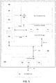
- FIG. 5 is a block diagram of a non-volatile data storage system, in accordance with one or more embodiments of the present disclosure.
- Data storage devices such as solid state drives (SSDs) typically include one or more controllers coupled with one or more non-volatile memory (NVM) arrays.
- NVM non-volatile memory
- Data stored on such memory arrays may be subject to loss and/or corruption. For example, data may be lost, damaged, corrupted, etc., due to failure of memory cells, damage (e.g., physical damage), degradation, read/write disturbs, loss of data retention, loss of endurance, etc.
- data written by applications also known as the primary data, may have a higher duplication ratio (the percentage of duplicate data in all data). For example, an application may write a series of images, one or more of which are already stored in the NVM array.
- a word processing application may attempt to save a document that is a duplicate of a document already stored in the NVM array. Removal of duplicate data significantly promotes space efficiency of NVM arrays and results in fewer write operations. Fewer write operations also benefits the lifetime of NVM arrays considering some. NVM's write endurance issues as a result of repeated write operations etc. Deduplication is an effective method used to reduce the write traffic of applications and can extend the lifespan of data storage devices such as SSDs.
- Deduplication calculates a fingerprint for a data chunk using a cryptographic hash function, like MD5, SHA-1 or SHA-256, and searches for a matching fingerprint in an existing fingerprints database (or metadata table) to determine whether the chunk is a duplicate of a chunk already stored in memory or not. Duplicate data may not be written/stored.
- the deduplication granularity can be a file, a chunk, a block, a page, a sector, a line, a word line, or some other appropriate unit of data, and the size of a chunk can be fixed or variable. Specific chunking methods may be used to identify the boundary between chunks.
- deduplication may be used to prevent writing redundant data (thereby extending the lifespan of a data storage device such as an SSD), it is more effective when the time saved avoiding writing duplicate data is more than the time used for identifying and managing duplicate data.
- Factors such as the level of resource contention among operations executing on the controller e.g., pre-fetching, data buffering and deduplication
- high levels of resource contention can correspond to a large amount of time required to identify and manage duplicate data.
- Embodiments of the present disclosure describes a method and apparatus for determining when deduplication is appropriate based on status information of the controller as well as media characteristics of the non-volatile memory.
- FIG. 1A is a diagram illustrating an example data storage system 100 , in accordance with some embodiments of the present disclosure.
- the data storage system 100 includes a computing device 110 and a data storage device 120 .
- the computing device 110 may also be referred to as a host system.
- the data storage device 120 may be part of the computing device 110 (e.g., may be located inside of a housing, chassis, ease, etc., of the computing device 110 ).
- the data storage device 120 may be separate from the computing device 110 (e.g., may be an external device that is coupled to the computing device 110 via a cable, such as a universal serial bus (USB) cable).
- USB universal serial bus
- the data storage device 120 may incorporate access command scheduling and/or execution in accordance with embodiments, examples, and/or implementations disclosed herein.
- the data storage device 120 may be any type of data storage device, drive, module, component, system, or the like.
- drive and data storage drive may be used herein in certain contexts to refer to any type of data storage device, and may be used substantially interchangeably with the term “data storage device” herein in connection with various embodiments and/or in various contexts.
- the data storage device 120 (e.g., hybrid hard drive, solid-state drive, any storage device utilizing solid-state memory, a hard disk drive, any storage device utilizing magnetic media/medium, etc.) includes a controller 130 (e.g., control circuitry, software, firmware, or a combination thereof) and a non-volatile memory 140 .
- a controller 130 e.g., control circuitry, software, firmware, or a combination thereof
- non-volatile memory 140 e.g., non-volatile memory
- the non-volatile memory (NVM) 140 may be configured far long-term storage of data and may retain data between power on/off cycles of the data storage device 120 .
- the non-volatile memory 140 and/or portions of the non-volatile memory 140 may also be referred to as a storage medium.
- the non-volatile memory 140 may include solid-state memory.
- Solid-state memory may comprise a wide variety of technologies, such as flash integrated circuits, Phase Change Memory (PC-RAM, PCM, or PRAM), Programmable Metallization Cell RAM (PMC-RAM or PMCm), Ovonic Unified Memory (OUM), Resistance RAM (RRAM) NAND memory (e.g., single-level coil (SLC) memory, multi-level cell (MLC) memory, triple level cell (TLC) memory, X4 or quad-level cell (QLC) memory, etc.), NOR memory, EEPROM, Ferroelectric Memory (FeRAM), magnetoresistive RAM (MRAM), or other discrete solid-state memory chips.
- PC-RAM Phase Change Memory
- PCM Phase Change Memory
- PMCm Programmable Metallization Cell RAM
- OFUM Ovonic Unified Memory
- RRAM Resistance RAM
- NAND memory e.g., single-level coil (SLC) memory, multi-level cell (MLC) memory, triple level cell (TLC) memory, X4 or quad-level cell (QLC)
- non-volatile memory 140 may comprise NAND flash memory having a certain access time for a unit of data, while in other embodiments non-volatile memory 140 may comprise fast NAND flash or storage class memory (SCM A.k.A. persistent memory), which has a faster access time for a unit of data than NAND flash memory.
- non-volatile memory may be a hybrid memory comprising both NAND flash memory and fast NAND flash or SCM.
- the non-volatile memory 140 may include any combination of the one or more types of memories described here.
- the non-volatile memory 140 may be divided logically and/or physically into arrays, planes, blocks, pages, tracks, and sectors. If the data storage device 120 is a hard disk drive, the non-volatile memory 140 may include magnetic recording heads coupled with rotating magnetic media.
- the controller 130 may include one or more processors, memory devices, data and/or power transmission channels/paths, boards, or the like.
- the controller 130 may be implemented as one or more system-on-a-chip (SoC) modules, field-programmable gate array (FPGA) modules, application-specific integrated circuit (ASIC) modules, processing devices (e.g., processors), chips, or the like.
- SoC system-on-a-chip
- FPGA field-programmable gate array
- ASIC application-specific integrated circuit
- processing devices e.g., processors
- one or more components of the controller 130 may be mounted on a printed circuit board (PCB).
- PCB printed circuit board
- the controller 130 may be configured to receive data commands from a storage interface (e.g., a device driver) residing on the computing device 110 .
- a storage interface e.g., a device driver
- the controller 130 may comprise a control processor 137 , memory device 135 .
- Memory device 135 may comprise a controller read-only memory and/or a controller volatile memory (e.g., DRAM).
- the memory device 135 of the controller 130 may include or otherwise be configured to store execution code of deduplication module 135 A, which may comprise code such as a set of instructions that configure the control processor 137 to provide aspects of the functionality described herein with respect to FIGS. 2, 3 and 4 for example. Alternatively or additionally, the control processor 137 can access code from the non-volatile memory 140 , such as a reserved area of memory cells in one or more word lines.
- deduplication module 135 A may allow controller 130 to determine whether data to be written to non-volatile memory 140 should be deduplicated based on status information of controller 130 as well as media characteristics of non-volatile memory 140 .
- Deduplication module 1355 A may utilize a machine learning algorithm trained on controller status information and media characteristics training data to determine whether data to be written should be deduplicated based on status information of controller 130 and the media characteristics of non-volatile memory 140 .
- Memory device 135 may also include or otherwise be configured to store a metadata table 135 B having strong and weak fingerprints for chunks of data that have been written to non-volatile memory 140 .
- a strong fingerprint value may be calculated for a chunk of data by applying an appropriate strong finger printing algorithm to it, such as a SHA-1 or SHA-256.
- a strong fingerprint value may be one that generates a larger fingerprint value (for example, 160 bits or more) and thus involves a large computational overhead (i.e. more storage requirements and processor usage) and longer processing time.
- calculating a strong fingerprint on a 4 KB data chunk using the SHA-1 algorithm may require 47548 processor cycles (using a 300 MHz processor) and the processing time may range from 80 microseconds to 6212 microseconds depending on the processor used. However, the probability of an accurate match with a strong fingerprint value may be higher (for example, 97% accuracy or better).
- a weak fingerprint value may be calculated for a chunk of data by applying an appropriate weak fingerprinting algorithm to it, such as CRC32 or Fletcher 32.
- a weak fingerprinting algorithm may be one that generates smaller fingerprint value (for example, 32 bits or less) and thus involves a small computational overhead i.e. less storage requirements and processor usage) and shorter processing time.
- calculating a weak fingerprint on a 4 KB data chunk using the CRC32 algorithm may require 4120 processor cycles (using a 300 MHz processor) and the processing time may range from 10 microseconds to 100 microseconds depending on the processor used.
- the probability of an accurate match with a weak fingerprint value may be lower (for example, 75% accuracy or better) than the probability of an accurate match when a strong fingerprinting algorithm is used.
- metadata table 135 B could be implemented or stored in non-volatile memory 140 .
- the controller 130 may communicate with the computing device 110 over a host interface 160 , and may receive commands via the host interface 160 . These commands may be referred to as data commands, data access commands, data storage access commands, etc. Data commands may specify a block address in the data storage device 120 . Data may be accessed/transferred based on such data commands. For example, the controller 130 may receive dam commands (from the computing device 110 ) and may execute such commands on/in the non-volatile memory 140 (e.g., in one or more arrays, pages, blocks, sectors, etc.). The data commands received from computing device 110 may include read data commands, write data commands, and erase data commands. The controller 130 may be coupled to the non-volatile memory (MINI) 140 via a NVM interface 150 .
- MINI non-volatile memory
- the NVM interface 150 may include a plurality of channels (e.g., one or more lines, pines, wires, traces, etc.) and each channel may be coupled to different portions of the non-volatile memory 140 (e.g., different NVM arrays, different flash arrays, etc.).
- channels e.g., one or more lines, pines, wires, traces, etc.
- each channel may be coupled to different portions of the non-volatile memory 140 (e.g., different NVM arrays, different flash arrays, etc.).
- the controller 130 may execute the received data commands to read, write, and erase data from non-volatile memory 140 , via the NVM interface 150 .
- the commands may include a read command (e.g. a data read command) to read a block of data from the non-volatile memory 140 .
- the controller 130 may read the data from the page and may transmit the data to the computing device 110 via the host interface 160 .
- the commands may include a write command (e.g., a data write command) to write data to a page in a non-volatile memory 140 .
- write commands may include program commands (e.g., a command to write the value “1” to a location the non-volatile memory 140 ) and erase commands (e.g., a command to write the value “0” to a location, a page, a block, etc., in the non-volatile memory array).
- the controller 130 may receive the data from the computing device 110 via the host interface 160 and may write the data to the page.
- the host interface 160 may include hardware wires, pins, traces, connectors, etc.), software (e.g., drivers), firmware, or a combination thereof, that allows the processing device 111 and/or the computing device 110 to communicate data with the data storage device 120 . Examples of a host interface may include a peripheral component interconnect express (PCIe) bus, a serial AT attachment (SATA) bus, a serial attached SCSI (SAS), a non-volatile memory express (NVMe) bus, etc.
- PCIe peripheral component interconnect express
- SATA serial AT attachment
- the data storage device 120 may store data received from the computing device 110 such that the data storage device 120 acts as data storage for the computing device 110 .
- the controller 130 may implement a logical interface.
- the logical interface may present to the computing device memory a set of logical addresses (e.g., sequential/contiguous addresses) where data may be stored.
- the controller 130 may map logical addresses to various physical memory addresses in the non-volatile memory arrays and/or other memory module(s) using a logical to physical mapping table.
- Mapping data indicating the mapping of logical addresses to physical memory addresses may be maintained in the data storage device. For example, mapping table data may be stored in non-volatile memory 140 in order to allow for recreation or recovery of mapping tables following a power cycle.
- the controller 130 may encode data when storing the data on the non volatile memory 140 .
- the controller 130 may encode the data to protect the data from errors, loss, corruption, etc.
- the controller 130 may protect the data from errors, loss, corruption, etc., using various methods, techniques, functions, operations, actions, etc.
- the controller 130 may protect the data by generating parity data (e.g., parity bits).
- the parity data may allow the controller 130 to determine whether there are errors in the data. (e.g., errors due to corruption, damaged cells, damaged blocks, error while reading the data, etc.).
- the parity data (e.g., one or more parity bits) may be generated using various algorithms, techniques, functions, operations, etc.
- the controller 130 may use an ECC to generate codewords.
- the codewords may also allow the controller 130 (e.g., a decoder—not shown in the Figures) to correct or recover from errors in the codewords.
- the controller 130 may also decode data that is stored on the non-volatile memory 140 .
- the decoder may decode codewords which encode the data that is stored on the non-volatile memory 140 .
- the decoder may perform error detection to determine the integrity of data retrieved from non-volatile memory 140 (e.g., to determine whether the data has errors). For example, the decoder may use parity data to cheek the data to determine whether there is an error in the data (e.g., whether one or more bits in the data, are incorrect due to corruption, damage cells, damaged blocks, etc.).
- Controller 130 may determine whether data to be written to non-volatile memory 140 is to be deduplicated using inline deduplication using status information of the controller 130 as well as media characteristics in information of the non-volatile memory 140 .
- Inline deduplication refers to deduplication of data that is performed as that data is being written to memory.
- Control processor 137 may retrieve status information about the controller 130 such as control processor utilization, temperature data, bandwidth, number of input/output operations per second, latency, buffer utilization, and pre-fetch status of the controller 130 .
- Control processor 137 may also retrieve media characteristics of the non-volatile memory 140 such as latency and residual bit error rate (RBER) among others.
- RBER residual bit error rate
- Control processor 137 may determine whether the data to be written should be deduplicated based on the status information of the controller 130 as well as the media characteristics of the non-volatile memory 140 . For example, controller 130 may determine that there is a high number of input/output operations per second, low bandwidth, and high latency and high processor utilization. This may indicate high levels of resource contention between deduplication and other controller functions, and thus control processor 137 may determine that inline deduplication should not be performed. This is because other controller functions such as data prefetching, data buffering, and other input output operations are all contending for the resources of control processor 137 . Control processor 137 may also determine that the latency and RBER of the non-volatile memory 140 are high. As a result, control processor 137 may determine that the time saved avoiding writing duplicate data would be less than the time used for identifying and managing duplicate data and thus may determine that inline deduplication should not be performed so as to utilize the resources of control processor 137 for other functions.
- control processor 137 may determine not to perform inline deduplication. In another example, if the control processor 137 determines that the temperature of controller 130 is too high, then control processor 137 may decide not to perform inline deduplication.
- the control processor 137 may utilize a machine learning algorithm (e.g., via execution of deduplication decision module 135 A) to make deduplication decisions based on status information and media characteristics.
- the deduplication decision module 135 A may include a set of decision making rules, such as if/else rules that govern the decision making process.
- FIG. 1A depicts a single data storage device
- the controller 130 could be implemented within a control unit or controller of a storage array or system, in which case, the functionalities described in the various embodiments would control data written to individual data storage devices of the storage array or system.
- FIG. 1B is a block diagram illustrating the exchange of data between the software modules in controller 130 of FIG. 1A , in accordance with some embodiments of the present disclosure.
- Controller 130 may include the deduplication decision maker 135 A (discussed further herein), the work load status collector module 135 C, the inline deduplication module 135 D and the offline deduplication module 135 E.
- Each software module may be stored in the memory device 135 and executed by control processor 137 (or otherwise implemented as discussed above) to perform the functions described with respect FIGS. 2,3 and 4 for example.
- Deduplication decision module 135 A may retrieve data storage device status information from the control processor 137 and media characteristics from non-volatile memory 140 and determine whether to perform inline or offline deduplication based on the data storage device status information 1350 and media characteristics 135 H as discussed in further detail herein. In some embodiments, deduplication decision module 135 A may determine whether to perform inline or offline deduplication further based on work load status information (as discussed further herein) of the data to be written, provided by work load status collector module 135 C. If deduplication decision module 135 A determines that inline deduplication should be performed for data being written, then inline deduplication module 135 D may be executed. If deduplication decision module 135 A determines that offline deduplication should be performed, then offline deduplication module 135 E may be executed.
- FIG. 1C is a diagram of a metadata table 135 B, illustrated in FIG. 1A , according to one embodiment.
- an entry of the metadata table has the same size as a cache line of control processor 137 .
- the first field 151 A of an entry has a tag and an ID of a deduplication transaction consisting of 8 bytes (denoted 8 B).
- Field 151 A provides a consistent way to reference a particular entry of metadata table 135 B.
- the second field 151 B is the reference count to indicate the number of references on a data chunk (i.e. the number of times data to be written has matched that data chunk).
- the third field 151 C is the chunk number. Note that each of the fields 151 A-C can be updated using an 8 byte atomic write.
- the fourth and fifth fields 151 D and 151 E store strong and weak fingerprints, respectively, for a data chunk, 32 bytes are sufficient for common strong cryptographic hash (fingerprinting) functions, such as MD5 (16 B), SHA-1 (20 B), and SHA-256 (32 B) while 4 bytes are used for weak fingerprinting functions such as CRC32 or Fletcher-32.
- the sixth field 151 F is a 1 byte flag to indicate whether the strong fingerprint is valid or not.
- the use of strong and weak fingerprints for a chunk allows for adaptive fingerprinting, as discussed herein.
- the last 3 bytes are padding bytes so that an entry has the same size as a cache line of control processor 137 .
- Metadata table 135 B jointly stores fingerprints, reference counts, and chunk numbers into one entry for a data chunk, which benefit both performance and consistency. Since metadata attributes of a chunk are likely to be successively used, fitting them into one cache line helps the control processor 137 to load them together and also eases the preservation of consistency.
- FIG. 2 is a flowchart illustrating an example method 200 for determining whether data should be deduplicated in the data storage system 100 when non-volatile memory 140 comprises a memory having an access time for a chunk (or other unit) of data that may be greater than the time required to calculate a fingerprint for the same chunk of data.
- Non-volatile memory 140 may be for example, NAND flash memory.
- the method 200 may be performed by a processing device (e.g., a processor, a central processing unit (CPU), a controller, an application-specific integrated circuit (ASIC), a field programmable gate array (FPGA), etc.), a neural network, etc.
- the method 200 may be performed by a processing device of a computing device, such as control processor 137 .
- the controller, processing device, and/or neural network may be processing logic that includes hardware (e.g., circuitry, dedicated logic, programmable logic, microcode, etc.), software (e.g., instructions run on a processor to perform hardware simulation), firmware, or a combination thereof.
- hardware e.g., circuitry, dedicated logic, programmable logic, microcode, etc.
- software e.g., instructions run on a processor to perform hardware simulation
- firmware e.g., firmware, firmware, or a combination thereof.
- control processor 137 may determine whether data to be written to non-volatile memory 140 is to be deduplicated using inline deduplication.
- Control processor 137 may retrieve status information about the controller 130 such as control processor utilization, temperature data, bandwidth, input/output operations per second (lops), latency, buffer utilization, and pre-fetch status of the controller 130 .
- Control processor 137 may also retrieve media characteristics of the non-volatile memory 140 such as latency and residual bit error rate (RBER) among others.
- RBER residual bit error rate
- control processor 137 may determine whether the data to be written should be deduplicated based on the status information of the controller 130 as well as the media characteristics of the non-volatile memory 140 .
- control processor 137 may determine whether data to be written to non-volatile memory 140 should be deduplicated further based on the work load status of the data to be written. For example, control processor 137 may consider whether the data is update, write, and/or read intensive based on the size, frequency and other characteristics of the data. Such work load status information may be collected and provided by work load status collector module 135 C (as discussed above with respect to FIG. 1B ).
- control processor 137 may write the data to non-volatile memory 140 .
- control processor 137 may proceed to block 270 and perform offline deduplication of the data (i.e., performing deduplication after the data has been written). Offline deduplication may be performed in the same manner as inline deduplication discussed herein.
- control processor 137 may determine a workload deduplication ratio of the data to be written and compare it to a threshold workload deduplication ratio.
- Control processor 137 may determine the threshold workload deduplication ratio based on factors including the average time to write a chunk of data, average time to calculate a strong fingerprint for a chunk of data, average time to calculate a weak fingerprint for a chunk of data, and the average time to search for a fingerprint in a metadata table. Control processor 137 may determine the workload deduplication ratio for the data using a workload monitor software module (not shown in the Figures) implementing methods such as periodical sampling.
- control processor 137 may calculate a strong fingerprint for the data.
- Control processor may utilize any appropriate strong fingerprinting algorithm such as SHA-1 or SHA-256 to generate a strong fingerprint for the data.
- control processor 137 may compare the strong fingerprint to each strong fingerprint value in a fingerprint metadata table (e.g., metadata table 135 B) and determine whether the strong fingerprint matches any values in the metadata table. If there is a match, then at block 230 control processor 137 may determine that the data to be written is duplicative of existing data stored in non-volatile memory 140 and update a logical to physical mapping (L2P) table.
- L2P logical to physical mapping
- control processor 137 may update the L2P table to indicate that the logical location of the data to be written corresponds to the physical location of the existing data already stored in non-volatile memory 140 . Stated differently, the data to be written already exists at the physical address in non-volatile memory 140 of the existing data already stored in non-volatile memory 140 . If there is no match (i.e. data to be written is not duplicative), then control processor 137 proceeds to block 210 where it may write the data to the non-volatile memory 140 .
- control processor 137 may calculate a weak fingerprint for the data.
- Control processor 137 may utilize any appropriate algorithm, such as CRC32 or Fletcher32 to calculate the weak fingerprint. Because calculating a strong fingerprint value is a computationally intensive and high latency operation, control processor 137 may first calculate a weak fingerprint before determining whether it is necessary to spend the resources computing a strong fingerprint.
- control processor 137 may compare the weak fingerprint value to each value in the metadata table. In response to determining that there is no matching value in the metadata table for the weak fingerprint, control processor 137 may proceed to block 210 where control processor 137 may write the data to the non-volatile memory 140 .
- control processor 137 may calculate a strong fingerprint for the data as discussed above with respect to block 220 .
- control processor 137 may compare the strong fingerprint value to each value in the metadata table and determine whether the strong fingerprint matches any values in the metadata table. If there is a match, then control processor 137 may proceed to block 230 where it may update the L2P table as discussed above. If there is no match, then control processor 137 proceeds to block 210 where it may write the data to the non-volatile memory 140 .
- FIG. 3 is a flowchart illustrating an example method 300 for determining whether data should be deduplicated in the data storage system 100 when non-volatile memory 140 comprises a memory having an access time for a chunk (or other unit) of data that may be less than die time required to calculate a fingerprint for the same chunk of data.
- the method 300 may be performed by a processing device (e.g., a processor, a central processing unit (CPU), a controller, an application-specific integrated circuit (ASIC), a field programmable gate array (FPGA), etc.), a neural network, etc.
- the method 300 may be performed by a processing device of a computing device, such as control processor 137 .
- the controller, processing device and/or neural network may be processing logic that includes hardware (e.g., circuitry, dedicated logic, programmable logic, microcode, etc.), software (e.g., instructions run on a processor to perform hardware simulation), firmware, or a combination thereof.
- hardware e.g., circuitry, dedicated logic, programmable logic, microcode, etc.
- software e.g., instructions run on a processor to perform hardware simulation
- firmware e.g., firmware, firmware, or a combination thereof.
- control processor 137 may determine whether data to be written to non-volatile memory 140 is to be deduplicated using inline deduplication as discussed above with respect to FIGS. 1A and 2 .
- Control processor 137 may retrieve status information about the controller 130 as well as media characteristics of the non-volatile memory 140 and determine whether the data to be written should be deduplicated based on the status information of the controller 130 as well as the media characteristics of the non-volatile memory 140 .
- control processor 137 may determine whether data to be written to non-volatile memory 140 should be deduplicated further based on the work load status of the data to be written. For example, control processor 137 may consider whether the data is update, write, and/or read intensive based on the size, frequency and other characteristics of the data.
- control processor 137 may write the data to non-volatile memory 140 . In some embodiments, control processor 137 may proceed to block 370 and perform offline deduplication of the data. At block 315 , in response to determining that the data to be written should be deduplicated, control processor 137 may calculate a weak fingerprint for the data. Control processor 137 may utilize any appropriate algorithm, such as CRC32 or Fletcher32 to calculate the weak fingerprint. At block 320 , control processor 137 may compare the weak fingerprint value to each value in the metadata table.
- control processor 137 may read data from the non-volatile memory 140 and at block 330 may compare the read data with the data to be written. Because calculating a strong fingerprint value is a computationally intensive and high latency operation, when non-volatile memory 140 comprises a memory having access time liar a unit of data that may be less than the time required to calculate a fingerprint for the same unit of data, control processor 137 may read the contents of non-volatile memory 140 and directly compare the data to be written to the contents read out of non-volatile memory 140 to determine if the data to be written is duplicative.
- control processor 137 may update the L2P table as discussed above with respect to FIG. 2 . If at block 330 the data to be written does not match any of the data read from the non-volatile memory 140 , then method 300 may proceed to block 310 where control processor 137 may write the data to non-volatile memory 140 .
- FIG. 4 is a flowchart illustrating an example method 400 for determining whether data should be deduplicated in the data storage system 100 when non-volatile memory 140 comprises a first memory comprising a memory having an access time for a chunk (or other unit) of data that may be greater than the time required to calculate a fingerprint for the same chunk of data (e.g., NAND flash) and a second memory comprising a memory having an access time for a chunk (or other unit) of data that may be less than the time required to calculate a fingerprint for the same chunk of data (e.g., fast NAND flash or SCM).
- a first memory comprising a memory having an access time for a chunk (or other unit) of data that may be greater than the time required to calculate a fingerprint for the same chunk of data (e.g., NAND flash)
- second memory comprising a memory having an access time for a chunk (or other unit) of data that may be less than the time required to calculate a fingerprint for the same chunk of data (e.g
- the method 400 may be performed by a processing device (e.g., a processor, a central processing unit (CPU), a controller, an application-specific integrated circuit (ASIC), a Field programmable gate array (FPGA), etc.), a neural network, etc.
- a processing device e.g., a processor, a central processing unit (CPU), a controller, an application-specific integrated circuit (ASIC), a Field programmable gate array (FPGA), etc.
- the method 400 may be performed by a processing device of a computing device such as control processor 137 .
- the controller, processing device, and/or neural network may be processing logic that includes hardware (e.g., circuitry, dedicated logic, programmable logic, microcode, etc.), software (e.g., instructions run on a processor to perform hardware simulation), firmware, or a combination thereof.
- control processor 137 may determine whether data to be written is to be written to the first memory or the second memory of non-volatile memory 140 . If control processor 137 determines that the data is to be written to the second memory, then control processor 137 may proceed to block 305 of method 300 , if control processor 137 determines that the data is to be written to the first memory, then control processor 137 may proceed to block 205 of method 200 ,
- FIG. 5 is a block diagram of an exemplary non-volatile data storage system 500 , which may be similar to data storage system 100 illustrated in FIG. 1 .
- the non-volatile data storage system 500 may include one or more memory die 502 .
- the memory die 502 includes a memory structure 504 of memory cells, such as an array of memory cells herein referred to as a memory array, address controller 506 and read/write circuits 530 .
- the memory structure 504 is addressable by word lines via a row decoder 528 and by bit lines via a column decoder 532 .
- the read/write circuits 530 include multiple sense blocks SB 1 , SB 2 , . . .
- the memory system-based control logic 404 is included in the same non-volatile memory system 500 (e.g., a removable storage card) as the one or more memory die 502 .
- Control commands and data are transferred between the host system 104 and memory system-based control logic 404 via a data bus 518 , and between the controller and the one or more memory die 502 via lines 516 .
- the data bus 518 may for example be a PCIe serial memory bus.
- the memory structure 504 can be 2D (laid out in a single fabrication plane) or 3D (laid out in multiple fabrication planes).
- the memory structure 504 may comprise one or more array of memory cells including a 3D array.
- the memory structure 504 may comprise a monolithic three-dimensional memory structure (3D array) in which multiple memory levels are conned above (and not in) a single substrate, such as a wafer, with no intervening substrates.
- the memory structure 504 may comprise any type of non-volatile memory that is monolithically formed in one or more physical levels of arrays of memory cells having an active area disposed above a silicon substrate.
- the memory structure 504 may be in a non-volatile memory device (e.g., non-volatile data storage system 500 ) having circuitry associated with the operation of the memory cells, whether the associated circuitry is above or within the substrate.
- the address controller 506 cooperates with the read/write circuits 530 to perform memory operations on memory cells of the memory structure 504 , and includes a state machine 508 , an address decoder 510 , and a power control 514 .
- the state machine 508 provides control of memory operations.
- a store region selector 512 may be provided, e.g., for programming parameters as described further below.
- the address decoder 510 provides an address interface between that used by the host or a memory system-based control logic 404 to the hardware address used by the row decoder 528 and column decoder 532 .
- the power control 514 controls the power and voltages supplied to the various control lines during memory operations.
- the power control 514 and/or read/write circuits 530 can include drivers for word lines, source gate select (SOS) transistors, drain gate select (DOS) transistors, bit lines, substrates (in 2D memory structures), charge pumps, and source lines.
- the sense blocks can include bit line drivers and sense amplifiers in one approach.
- An SOS transistor is a select gate transistor at a source end of a memory string
- a DOS transistor is a select gate transistor at a drain end of a memory string.
- a control circuit may include any one of, or a combination of, address controller 506 , state machine 508 , address decoder 510 , column decoder 532 , power control 514 , control processor 526 , sense blocks SB 1 , SB 2 , . . . , SBp, read write circuits 530 , memory system-based control logic 404 , and so forth.
- the memory system-based control logic 404 may comprise a control processor 526 and memory devices such as controller read-only memory 520 and controller volatile memory 522 .
- the memory devices of the memory system-based control logic 404 may comprise code such as a set of instructions that configure the control processor 526 to execute the set of instructions to provide aspects of the functionality described herein.
- the control processor 526 can access code from the memory structure 504 , such as a reserved area of memory cells in one or more word lines.
- code can be used by the memory system-based control logic 404 to access the memory structure 504 , controller read-only memory 520 , or controller volatile memory 522 for partial decoding and/or event detection logic.
- the control logic may utilize the host system volatile memory 524 for caching some or all of the raw video stream for partial decoding and event detection, using for example direct memory access technology (DMA) over the data bus 518 .
- DMA direct memory access technology
- the control logic may further include drivers to perform basic tasks such as controlling and allocating memory, prioritizing the processing of instructions, and controlling input and output ports.
- control logic can include software and other logic. (e.g., circuits, firmware) to perform the functions described herein.
- the control logic may comprise a sequencer to control the timing (start and stop times, durations, spacing etc.) of the various signals described herein.
- the state machine 508 may also be utilized to implement aspects of the control logic.
- the host system 104 is a computing device e.g., laptop, desktop, smartphone, tablet, digital camera) that includes one or more processors, one or more processor readable storage devices (host system volatile memory 524 , ROM, flash memory, hard disk drive, solid state memory) that store processor readable code (e.g., software) for programming the one or more processors to perform aspects of the techniques described herein.
- the host system 104 may also include additional system memory, one or more input/output interfaces and/or one or more input/output devices in communication with the one or more processors, as well as other components well known in the art.
- the store region selector 512 may be a non-volatile memory such as NAND flash memory, or another type.
- the store region selector 512 identifies blocks of the memory structure 504 for reading and writing, among other things, as known in the art.
- non-volatile memory system 500 is an example and that various implementations will include additional components, or exclude or combine some of the illustrated components, in manners known in the art.
- example or “exemplary” are used herein to mean serving as an example, instance, or illustration. Any aspect or design described herein as “example” or “exemplary” is not necessarily to be construed as preferred or advantageous over other aspects or designs. Rather, use of the words “example” or “exemplary” is intended to present concepts in a concrete fashion.
- the term “or” is intended to mean an inclusive “or” rather than an exclusive “or”. That is, unless specified otherwise, or clear from context, “X includes A or B” is intended to mean any of the natural inclusive permutations.
- All of the processes described above may be embodied in, and fully automated via, software code modules executed by one or more general purpose or special purpose computers or processors.
- the code modules may be stored on any type of computer-readable medium or other computer storage device or collection of storage devices. Some or all of the methods may alternatively be embodied in specialized computer hardware.
Landscapes
- Engineering & Computer Science (AREA)
- Theoretical Computer Science (AREA)
- Physics & Mathematics (AREA)
- General Engineering & Computer Science (AREA)
- General Physics & Mathematics (AREA)
- Human Computer Interaction (AREA)
- Information Retrieval, Db Structures And Fs Structures Therefor (AREA)
Abstract
Description
Claims (20)
Priority Applications (1)
| Application Number | Priority Date | Filing Date | Title |
|---|---|---|---|
| US16/367,900 US10789003B1 (en) | 2019-03-28 | 2019-03-28 | Selective deduplication based on data storage device controller status and media characteristics |
Applications Claiming Priority (1)
| Application Number | Priority Date | Filing Date | Title |
|---|---|---|---|
| US16/367,900 US10789003B1 (en) | 2019-03-28 | 2019-03-28 | Selective deduplication based on data storage device controller status and media characteristics |
Publications (2)
| Publication Number | Publication Date |
|---|---|
| US10789003B1 true US10789003B1 (en) | 2020-09-29 |
| US20200310667A1 US20200310667A1 (en) | 2020-10-01 |
Family
ID=72603829
Family Applications (1)
| Application Number | Title | Priority Date | Filing Date |
|---|---|---|---|
| US16/367,900 Active US10789003B1 (en) | 2019-03-28 | 2019-03-28 | Selective deduplication based on data storage device controller status and media characteristics |
Country Status (1)
| Country | Link |
|---|---|
| US (1) | US10789003B1 (en) |
Cited By (4)
| Publication number | Priority date | Publication date | Assignee | Title |
|---|---|---|---|---|
| US11126360B2 (en) * | 2019-10-22 | 2021-09-21 | International Business Machines Corporation | Dynamically adjusting block mode pool sizes |
| US11237984B2 (en) * | 2019-04-09 | 2022-02-01 | SK Hynix Inc. | Memory system, memory controller and operating method thereof |
| US11281610B2 (en) * | 2020-08-07 | 2022-03-22 | EMC IP Holding Company LLC | Method, device, and computer program product for managing data transfer |
| US11921644B2 (en) | 2022-05-20 | 2024-03-05 | Western Digital Technologies, Inc. | Optimizing huge page management |
Citations (14)
| Publication number | Priority date | Publication date | Assignee | Title |
|---|---|---|---|---|
| US20110125950A1 (en) * | 2009-11-24 | 2011-05-26 | International Business Machines Corporation | Systems and methods for performing deduplicated data processing on tape |
| US20110184908A1 (en) * | 2010-01-28 | 2011-07-28 | Alastair Slater | Selective data deduplication |
| CN102156727A (en) | 2011-04-01 | 2011-08-17 | 华中科技大学 | Method for deleting repeated data by using double-fingerprint hash check |
| US20130018853A1 (en) * | 2011-07-11 | 2013-01-17 | Dell Products L.P. | Accelerated deduplication |
| US20140114932A1 (en) * | 2012-10-18 | 2014-04-24 | Netapp, Inc. | Selective deduplication |
| US20140244598A1 (en) * | 2013-02-22 | 2014-08-28 | International Business Machines Corporation | Integrity checking and selective deduplication based on network parameters |
| US8825617B2 (en) | 2008-03-14 | 2014-09-02 | International Business Machines Corporation | Limiting deduplication based on predetermined criteria |
| CN105930101A (en) | 2016-05-04 | 2016-09-07 | 中国人民解放军国防科学技术大学 | Weak fingerprint repeated data deletion mechanism based on flash memory solid-state disk |
| US20170031830A1 (en) * | 2015-07-30 | 2017-02-02 | Netapp, Inc. | Deduplicated host cache flush to remote storage |
| US9612953B1 (en) * | 2014-01-16 | 2017-04-04 | Pure Storage, Inc. | Data placement based on data properties in a tiered storage device system |
| US9733836B1 (en) * | 2015-02-11 | 2017-08-15 | Violin Memory Inc. | System and method for granular deduplication |
| US20170286444A1 (en) * | 2016-03-29 | 2017-10-05 | International Business Machines Corporation | Region-integrated data deduplication implementing a multi-lifetime duplicate finder |
| US20180060367A1 (en) | 2016-08-29 | 2018-03-01 | International Business Machines Corporation | Workload optimized data deduplication using ghost fingerprints |
| US20180253255A1 (en) * | 2017-03-01 | 2018-09-06 | Tintri Inc. | Efficient deduplication for storage systems |
-
2019
- 2019-03-28 US US16/367,900 patent/US10789003B1/en active Active
Patent Citations (15)
| Publication number | Priority date | Publication date | Assignee | Title |
|---|---|---|---|---|
| US8825617B2 (en) | 2008-03-14 | 2014-09-02 | International Business Machines Corporation | Limiting deduplication based on predetermined criteria |
| US20110125950A1 (en) * | 2009-11-24 | 2011-05-26 | International Business Machines Corporation | Systems and methods for performing deduplicated data processing on tape |
| US20110184908A1 (en) * | 2010-01-28 | 2011-07-28 | Alastair Slater | Selective data deduplication |
| CN102156727A (en) | 2011-04-01 | 2011-08-17 | 华中科技大学 | Method for deleting repeated data by using double-fingerprint hash check |
| US20130018853A1 (en) * | 2011-07-11 | 2013-01-17 | Dell Products L.P. | Accelerated deduplication |
| US20140114932A1 (en) * | 2012-10-18 | 2014-04-24 | Netapp, Inc. | Selective deduplication |
| US9348538B2 (en) | 2012-10-18 | 2016-05-24 | Netapp, Inc. | Selective deduplication |
| US20140244598A1 (en) * | 2013-02-22 | 2014-08-28 | International Business Machines Corporation | Integrity checking and selective deduplication based on network parameters |
| US9612953B1 (en) * | 2014-01-16 | 2017-04-04 | Pure Storage, Inc. | Data placement based on data properties in a tiered storage device system |
| US9733836B1 (en) * | 2015-02-11 | 2017-08-15 | Violin Memory Inc. | System and method for granular deduplication |
| US20170031830A1 (en) * | 2015-07-30 | 2017-02-02 | Netapp, Inc. | Deduplicated host cache flush to remote storage |
| US20170286444A1 (en) * | 2016-03-29 | 2017-10-05 | International Business Machines Corporation | Region-integrated data deduplication implementing a multi-lifetime duplicate finder |
| CN105930101A (en) | 2016-05-04 | 2016-09-07 | 中国人民解放军国防科学技术大学 | Weak fingerprint repeated data deletion mechanism based on flash memory solid-state disk |
| US20180060367A1 (en) | 2016-08-29 | 2018-03-01 | International Business Machines Corporation | Workload optimized data deduplication using ghost fingerprints |
| US20180253255A1 (en) * | 2017-03-01 | 2018-09-06 | Tintri Inc. | Efficient deduplication for storage systems |
Non-Patent Citations (2)
| Title |
|---|
| Chen et al., "NF-Dedupe: A Novel No-fingerprint Deduplication Scheme for Flash-based SSDs", 20th IEEE Symposium on Computers and Communication (ISCC), 2015, pp. 588-594. |
| Wang et al., "NV-Dedup: High-Performance Inline Deduplication for Non-volatile Memory", IEEE Transactions on Computers, vol. 67, Issue 5, May 1, 2018, pp. 658-671. |
Cited By (4)
| Publication number | Priority date | Publication date | Assignee | Title |
|---|---|---|---|---|
| US11237984B2 (en) * | 2019-04-09 | 2022-02-01 | SK Hynix Inc. | Memory system, memory controller and operating method thereof |
| US11126360B2 (en) * | 2019-10-22 | 2021-09-21 | International Business Machines Corporation | Dynamically adjusting block mode pool sizes |
| US11281610B2 (en) * | 2020-08-07 | 2022-03-22 | EMC IP Holding Company LLC | Method, device, and computer program product for managing data transfer |
| US11921644B2 (en) | 2022-05-20 | 2024-03-05 | Western Digital Technologies, Inc. | Optimizing huge page management |
Also Published As
| Publication number | Publication date |
|---|---|
| US20200310667A1 (en) | 2020-10-01 |
Similar Documents
| Publication | Publication Date | Title |
|---|---|---|
| US10789003B1 (en) | Selective deduplication based on data storage device controller status and media characteristics | |
| US10795827B2 (en) | Adaptive management of intermediate storage | |
| US11615003B2 (en) | Optimized neural network data organization | |
| US11775389B2 (en) | Deferred error-correction parity calculations | |
| CN113076218B (en) | Method for rapidly processing data reading errors of NVM (non-volatile memory) chip and controller thereof | |
| CN114691535A (en) | Memory device, method of operating the same, and method of operating memory controller | |
| WO2022212566A1 (en) | Key storage for sorted string tables using content addressable memory | |
| US11188459B2 (en) | Data block switching at a memory sub-system | |
| US11169920B2 (en) | Cache operations in a hybrid dual in-line memory module | |
| US11126368B2 (en) | Systems and methods for finding a last good page in NAND open block | |
| US11636044B2 (en) | Logical-to-physical mapping | |
| US11586379B2 (en) | Memory system and method of operating the same | |
| CN113971001B (en) | Memory traffic pattern detection in a memory device | |
| CN113126906B (en) | Method and system for metadata indication | |
| CN115291796A (en) | Method and device for storing data | |
| US11966638B2 (en) | Dynamic rain for zoned storage systems | |
| US11983067B2 (en) | Adjustment of code rate as function of memory endurance state metric | |
| US11604749B2 (en) | Direct memory access (DMA) commands for noncontiguous source and destination memory addresses | |
| US20230185470A1 (en) | Method of operating memory system and memory system performing the same | |
| US20240126448A1 (en) | Adaptive read disturb scan | |
| US20230092380A1 (en) | Operation method of memory controller configured to control memory device | |
| US20220113903A1 (en) | Single memory bank storage for servicing memory access commands | |
| US20230110664A1 (en) | Managing a memory sub-system based on composite temperature | |
| CN113126899A (en) | Full multi-plane operation enablement | |
| TW202321926A (en) | Storage device and operating method thereof, and operating method of controller |
Legal Events
| Date | Code | Title | Description |
|---|---|---|---|
| AS | Assignment |
Owner name: WESTERN DIGITAL TECHNOLOGIES, INC., CALIFORNIA Free format text: ASSIGNMENT OF ASSIGNORS INTEREST;ASSIGNORS:SUN, CHAO;WANG, QINGBO;VUCINIC, DEJAN;REEL/FRAME:048732/0373 Effective date: 20190325 |
|
| FEPP | Fee payment procedure |
Free format text: ENTITY STATUS SET TO UNDISCOUNTED (ORIGINAL EVENT CODE: BIG.); ENTITY STATUS OF PATENT OWNER: LARGE ENTITY |
|
| AS | Assignment |
Owner name: JPMORGAN CHASE BANK, N.A., AS AGENT, ILLINOIS Free format text: SECURITY INTEREST;ASSIGNOR:WESTERN DIGITAL TECHNOLOGIES, INC.;REEL/FRAME:052915/0566 Effective date: 20200113 |
|
| STCF | Information on status: patent grant |
Free format text: PATENTED CASE |
|
| AS | Assignment |
Owner name: WESTERN DIGITAL TECHNOLOGIES, INC., CALIFORNIA Free format text: RELEASE OF SECURITY INTEREST AT REEL 052915 FRAME 0566;ASSIGNOR:JPMORGAN CHASE BANK, N.A.;REEL/FRAME:059127/0001 Effective date: 20220203 |
|
| AS | Assignment |
Owner name: JPMORGAN CHASE BANK, N.A., ILLINOIS Free format text: PATENT COLLATERAL AGREEMENT - A&R LOAN AGREEMENT;ASSIGNOR:WESTERN DIGITAL TECHNOLOGIES, INC.;REEL/FRAME:064715/0001 Effective date: 20230818 Owner name: JPMORGAN CHASE BANK, N.A., ILLINOIS Free format text: PATENT COLLATERAL AGREEMENT - DDTL LOAN AGREEMENT;ASSIGNOR:WESTERN DIGITAL TECHNOLOGIES, INC.;REEL/FRAME:067045/0156 Effective date: 20230818 |
|
| FEPP | Fee payment procedure |
Free format text: MAINTENANCE FEE REMINDER MAILED (ORIGINAL EVENT CODE: REM.); ENTITY STATUS OF PATENT OWNER: LARGE ENTITY |