US10756613B2 - Controlling current flow between nodes with adjustable back-gate voltage - Google Patents
Controlling current flow between nodes with adjustable back-gate voltage Download PDFInfo
- Publication number
- US10756613B2 US10756613B2 US15/886,322 US201815886322A US10756613B2 US 10756613 B2 US10756613 B2 US 10756613B2 US 201815886322 A US201815886322 A US 201815886322A US 10756613 B2 US10756613 B2 US 10756613B2
- Authority
- US
- United States
- Prior art keywords
- transistor
- node
- voltage
- terminal
- source
- Prior art date
- Legal status (The legal status is an assumption and is not a legal conclusion. Google has not performed a legal analysis and makes no representation as to the accuracy of the status listed.)
- Active, expires
Links
- 239000012212 insulator Substances 0.000 claims description 25
- 238000000034 method Methods 0.000 claims description 19
- 239000004065 semiconductor Substances 0.000 claims description 15
- 108091006146 Channels Proteins 0.000 description 30
- 239000000758 substrate Substances 0.000 description 15
- 239000000463 material Substances 0.000 description 11
- VYPSYNLAJGMNEJ-UHFFFAOYSA-N Silicium dioxide Chemical compound O=[Si]=O VYPSYNLAJGMNEJ-UHFFFAOYSA-N 0.000 description 6
- 238000002955 isolation Methods 0.000 description 6
- 238000010586 diagram Methods 0.000 description 5
- 239000002019 doping agent Substances 0.000 description 5
- 230000008569 process Effects 0.000 description 5
- 150000001875 compounds Chemical class 0.000 description 4
- VQCBHWLJZDBHOS-UHFFFAOYSA-N erbium(iii) oxide Chemical compound O=[Er]O[Er]=O VQCBHWLJZDBHOS-UHFFFAOYSA-N 0.000 description 4
- XUIMIQQOPSSXEZ-UHFFFAOYSA-N Silicon Chemical compound [Si] XUIMIQQOPSSXEZ-UHFFFAOYSA-N 0.000 description 3
- 229910052710 silicon Inorganic materials 0.000 description 3
- 239000010703 silicon Substances 0.000 description 3
- 239000000377 silicon dioxide Substances 0.000 description 3
- PNEYBMLMFCGWSK-UHFFFAOYSA-N aluminium oxide Inorganic materials [O-2].[O-2].[O-2].[Al+3].[Al+3] PNEYBMLMFCGWSK-UHFFFAOYSA-N 0.000 description 2
- 230000015556 catabolic process Effects 0.000 description 2
- 238000005516 engineering process Methods 0.000 description 2
- 230000001965 increasing effect Effects 0.000 description 2
- 150000002500 ions Chemical class 0.000 description 2
- 229910052751 metal Inorganic materials 0.000 description 2
- 239000002184 metal Substances 0.000 description 2
- 239000002135 nanosheet Substances 0.000 description 2
- SIWVEOZUMHYXCS-UHFFFAOYSA-N oxo(oxoyttriooxy)yttrium Chemical compound O=[Y]O[Y]=O SIWVEOZUMHYXCS-UHFFFAOYSA-N 0.000 description 2
- RVTZCBVAJQQJTK-UHFFFAOYSA-N oxygen(2-);zirconium(4+) Chemical compound [O-2].[O-2].[Zr+4] RVTZCBVAJQQJTK-UHFFFAOYSA-N 0.000 description 2
- 239000007787 solid Substances 0.000 description 2
- 239000000126 substance Substances 0.000 description 2
- 229910001928 zirconium oxide Inorganic materials 0.000 description 2
- GWEVSGVZZGPLCZ-UHFFFAOYSA-N Titan oxide Chemical compound O=[Ti]=O GWEVSGVZZGPLCZ-UHFFFAOYSA-N 0.000 description 1
- 230000004913 activation Effects 0.000 description 1
- 230000004888 barrier function Effects 0.000 description 1
- 239000003990 capacitor Substances 0.000 description 1
- 230000008859 change Effects 0.000 description 1
- 230000000295 complement effect Effects 0.000 description 1
- 238000004590 computer program Methods 0.000 description 1
- 229910052593 corundum Inorganic materials 0.000 description 1
- 230000007423 decrease Effects 0.000 description 1
- 230000001419 dependent effect Effects 0.000 description 1
- 230000008021 deposition Effects 0.000 description 1
- 239000003989 dielectric material Substances 0.000 description 1
- 239000012777 electrically insulating material Substances 0.000 description 1
- 229910052732 germanium Inorganic materials 0.000 description 1
- GNPVGFCGXDBREM-UHFFFAOYSA-N germanium atom Chemical compound [Ge] GNPVGFCGXDBREM-UHFFFAOYSA-N 0.000 description 1
- CJNBYAVZURUTKZ-UHFFFAOYSA-N hafnium(iv) oxide Chemical compound O=[Hf]=O CJNBYAVZURUTKZ-UHFFFAOYSA-N 0.000 description 1
- 238000002513 implantation Methods 0.000 description 1
- 230000006872 improvement Effects 0.000 description 1
- 238000011065 in-situ storage Methods 0.000 description 1
- 230000001939 inductive effect Effects 0.000 description 1
- 239000011810 insulating material Substances 0.000 description 1
- 238000004519 manufacturing process Methods 0.000 description 1
- 229910044991 metal oxide Inorganic materials 0.000 description 1
- 150000004706 metal oxides Chemical class 0.000 description 1
- 150000002739 metals Chemical class 0.000 description 1
- 230000004048 modification Effects 0.000 description 1
- 238000012986 modification Methods 0.000 description 1
- 230000001151 other effect Effects 0.000 description 1
- MMKQUGHLEMYQSG-UHFFFAOYSA-N oxygen(2-);praseodymium(3+) Chemical compound [O-2].[O-2].[O-2].[Pr+3].[Pr+3] MMKQUGHLEMYQSG-UHFFFAOYSA-N 0.000 description 1
- BPUBBGLMJRNUCC-UHFFFAOYSA-N oxygen(2-);tantalum(5+) Chemical compound [O-2].[O-2].[O-2].[O-2].[O-2].[Ta+5].[Ta+5] BPUBBGLMJRNUCC-UHFFFAOYSA-N 0.000 description 1
- HBMJWWWQQXIZIP-UHFFFAOYSA-N silicon carbide Chemical compound [Si+]#[C-] HBMJWWWQQXIZIP-UHFFFAOYSA-N 0.000 description 1
- 229910010271 silicon carbide Inorganic materials 0.000 description 1
- 235000012239 silicon dioxide Nutrition 0.000 description 1
- 229910001845 yogo sapphire Inorganic materials 0.000 description 1
Images


Classifications
-
- H—ELECTRICITY
- H02—GENERATION; CONVERSION OR DISTRIBUTION OF ELECTRIC POWER
- H02M—APPARATUS FOR CONVERSION BETWEEN AC AND AC, BETWEEN AC AND DC, OR BETWEEN DC AND DC, AND FOR USE WITH MAINS OR SIMILAR POWER SUPPLY SYSTEMS; CONVERSION OF DC OR AC INPUT POWER INTO SURGE OUTPUT POWER; CONTROL OR REGULATION THEREOF
- H02M1/00—Details of apparatus for conversion
-
- H—ELECTRICITY
- H01—ELECTRIC ELEMENTS
- H01L—SEMICONDUCTOR DEVICES NOT COVERED BY CLASS H10
- H01L29/00—Semiconductor devices specially adapted for rectifying, amplifying, oscillating or switching and having potential barriers; Capacitors or resistors having potential barriers, e.g. a PN-junction depletion layer or carrier concentration layer; Details of semiconductor bodies or of electrodes thereof ; Multistep manufacturing processes therefor
- H01L29/66—Types of semiconductor device ; Multistep manufacturing processes therefor
- H01L29/68—Types of semiconductor device ; Multistep manufacturing processes therefor controllable by only the electric current supplied, or only the electric potential applied, to an electrode which does not carry the current to be rectified, amplified or switched
- H01L29/76—Unipolar devices, e.g. field effect transistors
- H01L29/772—Field effect transistors
- H01L29/78—Field effect transistors with field effect produced by an insulated gate
- H01L29/786—Thin film transistors, i.e. transistors with a channel being at least partly a thin film
- H01L29/78645—Thin film transistors, i.e. transistors with a channel being at least partly a thin film with multiple gate
- H01L29/78648—Thin film transistors, i.e. transistors with a channel being at least partly a thin film with multiple gate arranged on opposing sides of the channel
-
- H—ELECTRICITY
- H01—ELECTRIC ELEMENTS
- H01L—SEMICONDUCTOR DEVICES NOT COVERED BY CLASS H10
- H01L29/00—Semiconductor devices specially adapted for rectifying, amplifying, oscillating or switching and having potential barriers; Capacitors or resistors having potential barriers, e.g. a PN-junction depletion layer or carrier concentration layer; Details of semiconductor bodies or of electrodes thereof ; Multistep manufacturing processes therefor
- H01L29/66—Types of semiconductor device ; Multistep manufacturing processes therefor
- H01L29/68—Types of semiconductor device ; Multistep manufacturing processes therefor controllable by only the electric current supplied, or only the electric potential applied, to an electrode which does not carry the current to be rectified, amplified or switched
- H01L29/76—Unipolar devices, e.g. field effect transistors
- H01L29/772—Field effect transistors
- H01L29/78—Field effect transistors with field effect produced by an insulated gate
- H01L29/786—Thin film transistors, i.e. transistors with a channel being at least partly a thin film
-
- H—ELECTRICITY
- H03—ELECTRONIC CIRCUITRY
- H03K—PULSE TECHNIQUE
- H03K17/00—Electronic switching or gating, i.e. not by contact-making and –breaking
-
- H—ELECTRICITY
- H03—ELECTRONIC CIRCUITRY
- H03K—PULSE TECHNIQUE
- H03K17/00—Electronic switching or gating, i.e. not by contact-making and –breaking
- H03K17/10—Modifications for increasing the maximum permissible switched voltage
- H03K17/102—Modifications for increasing the maximum permissible switched voltage in field-effect transistor switches
-
- H—ELECTRICITY
- H03—ELECTRONIC CIRCUITRY
- H03K—PULSE TECHNIQUE
- H03K17/00—Electronic switching or gating, i.e. not by contact-making and –breaking
- H03K17/30—Modifications for providing a predetermined threshold before switching
- H03K17/302—Modifications for providing a predetermined threshold before switching in field-effect transistor switches
-
- H—ELECTRICITY
- H02—GENERATION; CONVERSION OR DISTRIBUTION OF ELECTRIC POWER
- H02M—APPARATUS FOR CONVERSION BETWEEN AC AND AC, BETWEEN AC AND DC, OR BETWEEN DC AND DC, AND FOR USE WITH MAINS OR SIMILAR POWER SUPPLY SYSTEMS; CONVERSION OF DC OR AC INPUT POWER INTO SURGE OUTPUT POWER; CONTROL OR REGULATION THEREOF
- H02M1/00—Details of apparatus for conversion
- H02M1/0067—Converter structures employing plural converter units, other than for parallel operation of the units on a single load
- H02M1/0077—Plural converter units whose outputs are connected in series
-
- H02M2001/0077—
-
- H—ELECTRICITY
- H03—ELECTRONIC CIRCUITRY
- H03K—PULSE TECHNIQUE
- H03K2217/00—Indexing scheme related to electronic switching or gating, i.e. not by contact-making or -breaking covered by H03K17/00
- H03K2217/0018—Special modifications or use of the back gate voltage of a FET
Definitions
- Embodiments of the disclosure relate generally to controlling current flow between input and output nodes, and more particularly, to circuit structures for controlling current flow with adjustable back-gate voltages, and methods of operating the same.
- the various embodiments described herein can be used in a variety of applications, e.g., providing the functional equivalent of a transistor in a circuit structure with signal greater reliability.
- a transistor In electrical hardware, a transistor is a critical component for implementing digital and analog circuitry designs.
- a transistor includes three electrical terminals: a source, a drain, and a gate. By applying different voltages to the gate terminal, the flow of electric current between the source terminal and the drain terminal of the transistor can be switched on or off. The presence or absence of an applied voltage at the gate terminal of a transistor can be identified as “on” and “off” states of the transistor.
- transistors can serve as a switching element in various circuit designs, e.g., by manipulating a voltage applied to the gate of each transistor and thereby affecting the flow of electrical current between source and drain terminals of each transistor.
- RF radio frequency
- CMOS complementary metal-oxide semiconductors
- SOI semiconductor-on-insulator
- CMOS complementary metal-oxide semiconductors
- these low voltage devices have characteristics that make their use undesirable at high voltages.
- the use of Low voltage devices at high voltages requires the use of many stages and other circuit components, including capacitors, to reduce the possibility of circuit failure when using high voltages. The use and number of these components and stages reduce area efficiency and decreases the power efficiency of the circuit. In some cases, the use of low voltage tolerant devices at high voltages, could lead to component failure.
- a first aspect of the present disclosure provides a circuit structure including: a first transistor having a gate terminal, a source terminal, a drain terminal, and a back-gate terminal electrically coupled to an adjustable voltage source, wherein the gate terminal of the first transistor is electrically coupled to a first node having a first bias voltage; and a second transistor having a gate terminal, a source terminal electrically coupled to the drain terminal of the first transistor, a drain terminal, and a back-gate terminal electrically connected to the adjustable voltage source, wherein the gate terminal of the second transistor is electrically coupled to a second node having a second bias voltage, and wherein the adjustable voltage source is selectable between a first voltage and a second voltage to control a threshold voltage of the first transistor and a threshold voltage of the second transistor.
- a second aspect of the present disclosure provides a circuit structure including: first transistor having a gate terminal, a fully depleted semiconductor insulator (FDSOI) channel region positioned between a source terminal and a drain terminal, a back-gate terminal, separated from the FDSOI channel region with a buried insulator layer positioned beneath the FDSOI channel region, wherein the back-gate terminal is electrically coupled to an adjustable voltage source, and the gate terminal is electrically coupled to a first node having a first bias voltage; and a second transistor having a gate terminal, a source terminal electrically coupled to the drain terminal of the first transistor, a drain terminal, a FDSOI channel region positioned between the source and drain terminal, and a buried insulator positioned beneath the FDSOI channel region and a back-gate terminal, wherein the back-gate terminal is electrically connected to the adjustable voltage source, and a second node having a second bias voltage is electrically coupled to the gate terminal of the second transistor, and wherein the adjustable voltage source is selectable between
- a third aspect of the present disclosure provides a method for adjusting current flow between an input node and an output node, the method including: applying a first bias voltage to a first node electrically coupled to a gate terminal of a first transistor, wherein the first transistor further includes a source terminal electrically coupled to the input node, a drain terminal, and a back-gate terminal electrically coupled to an adjustable voltage source; applying a second biasing voltage to a second node electrically coupled to a gate terminal of a second transistor, wherein the second transistor further includes a source terminal electrically coupled to the drain terminal of the first transistor, a drain terminal electrically coupled to the output node, and a back-gate terminal electrically coupled to the adjustable voltage source; and shifting the adjustable voltage source from a first voltage to a second voltage, wherein the shifting reduces a threshold voltage of the first transistor to less than the first biasing voltage of the first node and reduces a threshold voltage of the second transistor to less than the second biasing voltage of the second node.
- FIG. 1 shows a cross-sectional view of a conventional transistor structure.
- FIG. 2 shows a cross-sectional view of a fully depleted SOI (FDSOI) transistor structure with a back-gate region beneath a buried insulator layer according to embodiments of the disclosure.
- FDSOI fully depleted SOI
- FIG. 3 shows a schematic view of a circuit structure according to embodiments of the disclosure.
- FIG. 4 shows a schematic view of the circuit structure with diodes according to embodiments of the disclosure.
- FIG. 5 shows a schematic view of the circuit structure with bias-regulating transistors according to embodiments of the disclosure.
- FIG. 6 shows a schematic view of the circuit structure with voltage-dividing resistors according to embodiments of the disclosure.
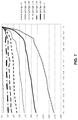
- FIG. 7 shows a representative plot of current flow (in microamperes) versus input-output voltage for the circuit structure at varying back-gate voltages.
- FIG. 8 shows a group of plots comparing input-output voltage for a circuit structure according to the disclosure with conventional transistor structures.
- FIG. 9 shows an example of a process flow diagram for controlling current flow between input and output nodes of the circuit structure according to embodiments of the disclosure.
- a macro-transistor is comprised of at least two electrically coupled transistors. Each individual transistor has a gate terminal and a back-gate terminal where voltage can be applied. This transistor structure, found in FDSOI transistors, varies significantly from conventional transistors structure as described herein.
- An adjustable voltage is applied to each of the back-gate terminals of the transistors and is generally used as the primary driving gate.
- a biasing voltage is applied to each of the gate terminals at different levels to evenly distribute the drain-source voltage of the individual transistors. This effectively changes the threshold voltage of the back-gate terminals of the individual transistors and controls the flow of current through the macro transistor.
- This macro transistor circuit structure allows a low voltage device to function at high voltages, such as with charge pumps, without the use of multiple stages and extra components as required in traditional circuit structures performing similar processes. Reducing the number of stages and components not only increases power efficiency, but also reduces the overall volume of the circuit structure.
- a conventional transistor 12 is depicted as an example to emphasize structural and operational differences relative to embodiments of the present disclosure, and transistor elements included therein.
- Conventional transistor 12 may be fabricated, e.g., by way of conventional fabrication techniques which may operate on a bulk silicon substrate.
- Conventional transistor 12 thus may be formed in a substrate 20 including, e.g., one or more semiconductor materials.
- the entirety of substrate 20 or a portion thereof may be strained.
- Source and drain nodes S, D of conventional transistor 12 may be coupled to regions of substrate 20 which include conductive dopants therein, e.g., a source region 28 and a drain region 30 separated by a channel region 26 .
- a gate region 32 formed on channel region 26 can be coupled to a gate node G to control a conductive channel within channel region 26 .
- a group of trench isolations 34 may be formed from electrically insulating materials such that regions 26 , 28 , 30 are laterally separated from parts of other transistors. As shown, trench isolations 34 form an insulating barrier between terminals 36 and regions 26 , 28 , 30 and/or other elements. Further features of each element in conventional transistor 12 (e.g., function and material composition) are described in detail elsewhere herein relative to similar components in an FDSOI transistor 102 ( FIG. 2 ) according to embodiments of the disclosure.
- FIG. 2 a cross-sectional view of a type of fully depleted semiconductor on insulator (FDSOI) transistor 102 which may be deployed, e.g., in structures and methods according to the disclosure, is shown.
- FDSOI transistor 102 can be formed with structural features for reducing the electrical resistance across source and drain terminals S, D thereof.
- FDSOI transistor 102 and components thereof can be formed on and within a substrate 120 .
- Substrate 120 can include any currently known or later-developed semiconductor material including, without limitation, one or more of the example semiconductor materials described elsewhere herein relative to substrate 20 ( FIG. 1 ).
- a back-gate region 122 can be implanted or formed in-situ during deposition with one or more doping compounds to change the electrical properties thereof.
- Doping generally refers to a process by which foreign materials (“dopants”) are added to a semiconductor structure to alter its electrical properties, e.g., resistivity and/or conductivity. Where a particular type of doping (e.g., p-type or n-type) doping is discussed herein, it is understood that an opposite doping type may be implemented in alternative embodiments.
- Implantation refers to a process in which ions are accelerated toward a solid surface to penetrate the solid up to a predetermined range based on the energy of the implanted ions.
- back-gate region 122 can include the same material composition as the remainder of substrate 120 , but can additionally include dopant materials therein.
- a buried insulator layer 124 also known in the art as a “buried oxide” or “BOX” layer, can separate back-gate region 122 of substrate 120 from source/drain regions 126 and a channel region 127 of FDSOI transistor 102 . Buried insulator layer 124 therefore may be composed of one or more oxide compounds, and/or any other currently known or later-developed electrically insulative substances.
- FDSOI transistor 102 therefore can be embodied as a “fully-depleted semiconductor on insulator” (FDSOI) structure, distinguishable from other structures (e.g., conventional transistor 12 ( FIG. 1 )) by including a dopant depleted channel region 127 , buried insulator layer 124 , back-gate nodes BG, etc., thereby allowing technical advantages such as an adjustable electric potential within back-gate region 122 of FDSOI transistor 102 as discussed elsewhere herein.
- FDSOI semiconductor on insulator
- FDSOI transistor 102 is shown and described as being formed with a particular arrangement of substrate 120 , back-gate regions 122 , and buried insulator layer 124 , it is understood that FDSOI transistor 102 may alternatively be structured as a fin transistor, a nanosheet transistor, a vertical transistor, and/or one or more other currently-known or later-developed transistor structures for providing a back-gate terminal for adjusting the transistor's threshold voltage.
- Source/drain regions 126 and channel region 127 may electrically couple a first drain terminal 128 of FDSOI transistor 102 to a second drain terminal 130 of FDSOI transistor 102 when the transistor is in an on state.
- a gate stack 132 can be positioned over channel region 127 , such that a voltage of gate node G controls the electrical conductivity between first and second drain terminals 128 , 130 through source/drain regions 126 and channel region 127 .
- Gate stack 132 can have, e.g., one or more electrically conductive metals therein, in addition to a gate dielectric material (indicated with black shading between bottom of stack and channel region 127 ) for separating the conductive metal(s) of gate stack 132 from at least channel region 127 .
- trench isolations 134 can electrically and physically separate the various regions of FDSOI transistor 102 from parts of other transistors.
- Trench isolations 134 may be composed of any insulating material such as SiO 2 or a “high-k” dielectric having a high dielectric constant, which may be, for example, above 3.9. In some situations, trench isolations 134 may be composed of an oxide substance.
- Materials appropriate for the composition of trench isolations 134 may include, for example, silicon dioxide (SiO 2 ), hafnium oxide (HfO 2 ), alumina (Al 2 O 3 ), yttrium oxide (Y 2 O 3 ), tantalum oxide (Ta 2 O 5 ), titanium dioxide (TiO 2 ), praseodymium oxide (Pr 2 O 3 ), zirconium oxide (ZrO 2 ), erbium oxide (ErO x ), and other currently known or later-developed materials having similar properties.
- Back-gate region 122 can be electrically coupled to back-gate node BG through back-gate terminals 136 within substrate 120 to further influence the characteristics of amplifier circuit 102 , e.g., the conductivity between first and second drain terminals 128 , 130 through source/drain regions 126 and channel region 127 .
- Applying an electrical potential to back-gate terminals 136 at back-gate node BG can induce an electric charge within back-gate region 122 , thereby creating a difference in electrical potential between back-gate region 122 and source/drain regions 126 , channel region 127 , across buried insulator layer 124 .
- this difference in electrical potential between elements can affect the threshold voltage of FDSOI transistor 102 , i.e., the minimum voltage for inducing electrical conductivity across source/drain and channel regions 126 , 127 between first and second drain terminals 128 , 130 as discussed herein.
- applying a back-gate biasing voltage to back-gate terminals 136 can lower the threshold voltage of FDSOI transistor 102 , thereby reducing source drain resistance and increasing drain current, relative to the threshold voltage of FDSOI transistor 102 when an opposite voltage bias is applied to back-gate terminals 136 .
- FDSOI transistor 102 can allow a reduced width (saving silicon area) relative to conventional applications and transistor structures.
- a width of source/drain and channel regions 126 , 127 i.e., into and out of the plane of the page
- a length of source/drain and channel regions 126 , 127 (i.e., left to right within the plane of the page) between first and second drain terminals 128 , 130 can be, e.g., approximately twenty nanometers (nm).
- FDSOI technology transistors e.g., FDSOI transistor 102
- FDSOI transistor 102 offer the ability to apply a voltage bias to back-gate region 122 to manipulate the threshold voltage V t (i.e., minimum voltage for channel activation) of FDSOI transistor 102 .
- V t i.e., minimum voltage for channel activation
- applying calibration voltages to back-gate region 122 can allow a user to reduce the local oscillator (LO) leakage and improve the linearity of an electronic transmitter.
- Back-gate region 122 can be coupled to an adjustable voltage to permit adjustment and calibration of the threshold voltage of FDSOI transistor 102 .
- any transistor which includes a back-gate terminal can be an embodiment of FDSOI transistor 102 .
- Other transistors without back-gate terminals may alternatively take the form of any currently known or later developed transistor structure configured for use in a structure with FDSOI transistors 102 .
- FIG. 3 depicts an embodiment of the basic macro-transistor 200 circuit structure.
- the technical advantages and features described herein can be attainable by using embodiments of the FDSOI transistor 102 ( FIG. 2 ) for each individual transistor element of macro-transistor 200 circuit structure.
- FDSOI transistor 102 is shown in FIG. 2 , it is understood that FDSOI transistor 102 may alternatively be structured as a fin transistor, a nanosheet transistor, a vertical transistor, and/or one or more other transistor described as being formed with a particular arrangement of a gate terminal, also referred to as a gate stack 132 in FIG. 2 , and a back-gate terminal 136 .
- First transistor 204 may include a gate terminal 208 , a source terminal 210 , a drain terminal 212 , and a back-gate terminal 214 .
- the second transistor may include a gate terminal 216 , a source terminal 218 , a drain terminal 220 , and a back-gate terminal 222 .
- the drain terminal 212 of first transistor 204 can be electrically coupled to source terminal 218 of second transistor 206 , allowing source terminal 210 to act as a macro-source (MS) of the macro-transistor 200 and drain terminal 220 to act as a macro-drain (MD) of the macro transistor.
- Back-gate terminals 214 and 222 are electrically coupled to an adjustable voltage source V s . During operational conditions, back-gate terminals 214 and 222 are act as a macro-gate (MG) of macro-transistor 200 .
- Gate terminal 208 of first transistor 204 is electrically coupled to a first node N 1 where a first biasing voltage BV 1 can be applied.
- Gate terminal 216 of second transistor 206 is electrically coupled to a second node N 2 , where a second biasing voltage BV 2 can also be applied.
- Biasing voltages BV 1 and BV 2 are varied at different voltages using other circuit components, including but not limited to diodes, diode-connected MOS transistors, resistors, or any combination of these components, to allow the drain to source voltage V ds , also referred to as the threshold voltage, of the individual transistors to be evenly distributed.
- the threshold voltage controls the flow of current in transistor channel region 26 , as viewed in FIG. 2 .
- the number of individual transistors in macro circuit 200 is dependent on the threshold voltage each individual transistor experiences during circuit operation.
- First and second biasing voltages BV 1 and BV 2 maintain the threshold voltage of the individual transistors to be within the individual transistors' breakdown limits.
- the adjustable voltage source V s may be adjustable between at least a first voltage 228 and a second voltage 230 to regulate the threshold voltage ( 232 , 234 , respectively) of the individual transistors 204 and 206 .
- the circuit structure of macro-transistor 200 may be configured to allow a first voltage 228 of adjustable voltage source V s to increase the threshold voltage 232 of first transistor 204 to more than first bias voltage BV 1 .
- This configuration can also increase threshold voltage 234 of second transistor 206 to an amount greater than second bias voltage BV 2 .
- a second voltage 230 of the adjustable voltage source V s can also be configured to reduce threshold voltage 232 of first transistor 204 to an amount less than first bias voltage BV 1 .
- This configuration using second voltage 232 also reduces the threshold voltage of the second transistor to less than the second bias voltage.
- FIG. 3 provides an example of a PMOS macro-transistor, situations where NMOS transistors and materials are used, the embodiments discussed herein may also be configured to form a NMOS macro-transistor.
- FIG. 4 demonstrates an embodiment of macro-transistor 200 using diodes 302 to bias gate terminals 208 and 216 .
- first node N 1 may be positioned proximate to source terminal 210 of first transistor 204 , and electrically coupled to gate terminal 208 , where first biasing voltage BV 1 may be applied as shown in FIG. 3 .
- First node N 1 is electrically coupled to second node N 2 through at least one diode 302 , though a plurality of diodes may be used as shown in FIG. 4 .
- Second node N 2 can be electrically coupled to gate terminal 216 and drain source 220 of second transistor 206 .
- a third node N 3 may exist between the diodes 302 or other electrical components.
- This third node N 3 can be electrically connected to either drain terminal 212 of first transistor 204 or source terminal 218 of second transistor 206 depending on desired threshold voltage 232 , 234 of first and second transistor 204 and 206 respectively, as generally shown in FIG. 2 . While the polarity described above can be viewed as PMOS, NMOS polarity and orientation may also be used.
- FIGS. 3 and 5 together provides an alternative embodiment of a macro-transistor using bias-regulating transistors 402 to influence first and second biasing voltages BV 1 and BV 2 .
- First node N 1 may be positioned near source terminal 210 of first transistor 204 , and can be electrically coupled to gate terminal 208 .
- First node N 1 can also be electrically coupled to second node N 2 , positioned near drain terminal 220 of the second transistor 206 , through at least one bias-regulating transistor 402 .
- FIG. 5 demonstrates how a plurality of bias-regulating transistors 402 , connected in series between first node N 1 and second node N 2 , may be configured.
- a plurality of bias-regulating transistors may also be arranged in parallel to additionally affect the voltage and current of macro-transistor 200 .
- additional nodes such as a third node N 3 existing between two bias-regulating transistors 402 , may be electrically coupled to drain terminal 212 of first transistor 204 and/or the source terminal 218 of the second transistor 206 , as generally shown in FIG. 5 .
- First node N 1 may be positioned at gate terminal 210 of first transistor 204 .
- First node N 1 may be electrically coupled to a second node N 2 through a voltage dividing tap 502 or other resistor configuration.
- the resistors of the voltage dividing tap 502 may be configured either in series or in parallel.
- second node N 2 may be electrically coupled directly to gate terminal 216 of second transistor 206 and electrically coupled to drain terminal 220 of second transistor 206 through at least one resistor or other electrical component, as generally shown in FIG. 6 . All of the aforementioned electrical components may be used as described above or in combination with other components.
- FIG. 7 depicts a plot showing that the aforementioned low voltage components of a macro-transistor are operable in circuit environments having higher voltages.
- the plot shows the source to gate voltage V gs as current I( ⁇ A) is increased.
- V gs increases and conductance increases a channel is formed, i.e., a macro-gate.
- FIG. 8 shows a group of plots comparing input-output voltage for a circuit structure having a macro-transistor 200 and the individual transistors 204 and 206 , as shown in FIG. 3 .
- Plots A and B of FIG. 8 demonstrate expected behavior and threshold voltages 232 , 234 at back-gate terminals 214 , 222 , of first and second transistor 204 , 206 , as shown in FIG. 3 .
- Plots C and D of FIG. 8 demonstrate that source to gate voltage V gs and drain to source voltage of macro-transistor 200 behave as expected and maintain the expected voltages without breakdown of the circuit structure.
- embodiments of the disclosure include methods for adjusting current flow between an input node 236 and an output node 238 , e.g., through the operation of macro-transistor 200 ( FIGS. 2-6 ) described herein.
- Methods according to the disclosure can include, applying a first bias voltage BV 1 to a first node N 1 electrically coupled to a gate terminal 208 of a first transistor 204 , step S 1 .
- First transistor 204 may further include a source terminal 210 electrically coupled to an input node 236 a drain terminal 212 , and a back-gate terminal 214 electrically coupled to an adjustable voltage source V s .
- a second bias voltage BV 2 may be applied to a second node N 2 , step S 2 .
- Second node N 2 may be electrically coupled to gate terminal 216 of second transistor 206 .
- Second transistor 206 may further include a source terminal 218 that is electrically coupled to drain terminal 220 of first transistor 204 .
- Drain terminal 220 may be electrically coupled to output node 238 , and a back-gate terminal 234 .
- Back-gate terminal 234 can then be electrically 222 coupled to the adjustable voltage source V s .
- Adjustable voltage source V s may then be shifted from a first voltage 228 to a second voltage 230 , step S 3 of FIG. 9 . Shifting between a first voltage 228 and a second voltage 230 , reduces the threshold voltage 232 of the first transistor 204 to less than first biasing voltage BV 1 of first node N 1 . This also reduces the threshold voltage 234 of second transistor 206 to less than second biasing voltage BV 2 of second node N 1 .
- first and second transistors 204 , 206 By shifting from first voltage 228 to second voltage 230 allows first and second transistors 204 , 206 to operate as a single transistor or macro-transistor 200 , wherein back-gate terminals 214 , 222 of first and second transistor 204 and 206 may be used as a single gate terminal or macro-gate MG.
- First transistor 204 and second transistor 206 may be a fully depleted semiconductor on insulator (FDSOI) transistors with a channel region 127 positioned laterally between first drain terminal 128 and second drain terminal 130 , of first 204 or second transistor 206 , as shown in FIGS. 2-3 .
- a buried insulator layer 124 may be positioned beneath FDSOI channel region 127 and buried insulator layer 124 .
- Buried oxide layer 127 separates back-gate terminal 136 of first 204 or second transistor 206 from FDSOI channel region 127 .
- each block in the flowchart or block diagrams may represent a module, segment, or portion of code, which comprises one or more executable instructions for implementing the specified logical function(s).
- the functions noted in the block may occur out of the order noted in the figures. For example, two blocks shown in succession may, in fact, be executed substantially concurrently, or the blocks may sometimes be executed in the reverse order, depending upon the functionality involved.
Landscapes
- Engineering & Computer Science (AREA)
- Power Engineering (AREA)
- Microelectronics & Electronic Packaging (AREA)
- Physics & Mathematics (AREA)
- Ceramic Engineering (AREA)
- Condensed Matter Physics & Semiconductors (AREA)
- General Physics & Mathematics (AREA)
- Computer Hardware Design (AREA)
- Thin Film Transistor (AREA)
- Metal-Oxide And Bipolar Metal-Oxide Semiconductor Integrated Circuits (AREA)
Abstract
Description
Claims (20)
Priority Applications (1)
| Application Number | Priority Date | Filing Date | Title |
|---|---|---|---|
| US15/886,322 US10756613B2 (en) | 2018-02-01 | 2018-02-01 | Controlling current flow between nodes with adjustable back-gate voltage |
Applications Claiming Priority (1)
| Application Number | Priority Date | Filing Date | Title |
|---|---|---|---|
| US15/886,322 US10756613B2 (en) | 2018-02-01 | 2018-02-01 | Controlling current flow between nodes with adjustable back-gate voltage |
Publications (2)
| Publication Number | Publication Date |
|---|---|
| US20190238044A1 US20190238044A1 (en) | 2019-08-01 |
| US10756613B2 true US10756613B2 (en) | 2020-08-25 |
Family
ID=67393747
Family Applications (1)
| Application Number | Title | Priority Date | Filing Date |
|---|---|---|---|
| US15/886,322 Active 2038-10-29 US10756613B2 (en) | 2018-02-01 | 2018-02-01 | Controlling current flow between nodes with adjustable back-gate voltage |
Country Status (1)
| Country | Link |
|---|---|
| US (1) | US10756613B2 (en) |
Cited By (1)
| Publication number | Priority date | Publication date | Assignee | Title |
|---|---|---|---|---|
| US11368016B2 (en) | 2020-03-18 | 2022-06-21 | Mavagail Technology, LLC | ESD protection for integrated circuit devices |
Families Citing this family (2)
| Publication number | Priority date | Publication date | Assignee | Title |
|---|---|---|---|---|
| US10756613B2 (en) * | 2018-02-01 | 2020-08-25 | Marvell Asia Pte, Ltd. | Controlling current flow between nodes with adjustable back-gate voltage |
| US10775826B2 (en) * | 2018-11-20 | 2020-09-15 | Globalfoundries Inc. | Back-gate biasing voltage divider topology circuit structure |
Citations (34)
| Publication number | Priority date | Publication date | Assignee | Title |
|---|---|---|---|---|
| US5663589A (en) * | 1993-09-29 | 1997-09-02 | Seiko Instruments Inc. | Current regulating semiconductor integrated circuit device and fabrication method of the same |
| US6292056B1 (en) * | 2000-07-06 | 2001-09-18 | Credence Systems Corporation | Differential amplifier with adjustable common mode output voltage |
| US6353357B1 (en) * | 1999-10-20 | 2002-03-05 | Infineon Technologies Ag | Controlling transistor threshold potentials using substrate potentials |
| US20020044076A1 (en) * | 2000-08-30 | 2002-04-18 | Chi-Tai Yao | Current-steering D/A converter and unit cell |
| US20020140458A1 (en) * | 2001-03-28 | 2002-10-03 | Masatoshi Sato | CMOS inverter |
| US6466077B1 (en) * | 1999-09-13 | 2002-10-15 | Hitachi, Ltd. | Semiconductor integrated circuit device including a speed monitor circuit and a substrate bias controller responsive to the speed-monitor circuit |
| US20030005378A1 (en) * | 2001-06-28 | 2003-01-02 | Intel Corporation | Body bias using scan chains |
| US20060017494A1 (en) * | 2004-07-26 | 2006-01-26 | Masashi Horiguchi | Semiconductor integrated circuit device |
| US20060091936A1 (en) * | 2004-11-01 | 2006-05-04 | Nec Corporation | Semiconductor integrated circuit device |
| US20070267701A1 (en) * | 2006-05-22 | 2007-11-22 | Myung-Hee Sung | Electrostatic discharge circuit and method for reducing input capacitance of semiconductor chip including same |
| US20090160531A1 (en) * | 2007-12-20 | 2009-06-25 | Ati Technologies Ulc | Multi-threshold voltage-biased circuits |
| US20110205673A1 (en) * | 2010-02-23 | 2011-08-25 | Renesas Electronics Corporation | Semiconductor device including electrostatic protection circuit |
| US20110260780A1 (en) * | 2010-04-27 | 2011-10-27 | Rf Micro Devices, Inc. | High power fet switch |
| US20130020644A1 (en) * | 2011-07-22 | 2013-01-24 | Renesas Electronics Corporation | Semiconductor device |
| US20140008732A1 (en) * | 2011-11-14 | 2014-01-09 | Sami Hyvonen | Macro-transistor devices |
| US20140009214A1 (en) * | 2012-07-07 | 2014-01-09 | Skyworks Solutions, Inc. | Circuits, devices, methods and applications related to silicon-on-insulator based radio-frequency switches |
| US20140023173A1 (en) * | 2012-07-20 | 2014-01-23 | Semiconductor Energy Laboratory Co., Ltd. | Pulse output circuit, display device, and electronic device |
| US8659346B2 (en) * | 2009-07-15 | 2014-02-25 | Spansion Llc | Body-bias voltage controller and method of controlling body-bias voltage |
| US20150028930A1 (en) * | 2013-07-24 | 2015-01-29 | Stmicroelectronics Sa | Variable Delay Element |
| US20150054571A1 (en) * | 2013-08-21 | 2015-02-26 | Semiconductor Energy Laboratory Co., Ltd. | Charge pump circuit and semiconductor device including the same |
| US20150263707A1 (en) * | 2014-03-17 | 2015-09-17 | Stmicroelectronics International N.V. | Schmitt trigger in fdsoi technology |
| US20150326207A1 (en) * | 2014-05-12 | 2015-11-12 | Huawei Technologies Co., Ltd. | Switch, antenna tuner, and radio frequency apparatus |
| US9201440B2 (en) * | 2013-06-21 | 2015-12-01 | Renesas Electronics Corporation | Semiconductor integrated circuit device |
| US9385708B2 (en) * | 2014-03-17 | 2016-07-05 | Stmicroelectronics International N.V. | Methodology to avoid gate stress for low voltage devices in FDSOI technology |
| US20170154909A1 (en) * | 2015-11-30 | 2017-06-01 | Semiconductor Energy Laboratory Co., Ltd. | Signal processing circuit and semiconductor device including the signal processing circuit |
| US20170186473A1 (en) * | 2015-12-29 | 2017-06-29 | Semiconductor Energy Laboratory Co., Ltd. | Semiconductor device, electronic device, and semiconductor wafer |
| US20170271516A1 (en) * | 2016-03-18 | 2017-09-21 | Semiconductor Energy Laboratory Co., Ltd. | Semiconductor device, semiconductor wafer, and electronic device |
| US20180048305A1 (en) * | 2016-08-09 | 2018-02-15 | Skyworks Solutions, Inc. | Radio-frequency switch with switchable capacitor |
| US20180131369A1 (en) * | 2016-11-10 | 2018-05-10 | Skyworks Solutions, Inc. | Manifolded gate resistance network |
| US10236872B1 (en) * | 2018-03-28 | 2019-03-19 | Psemi Corporation | AC coupling modules for bias ladders |
| US20190238044A1 (en) * | 2018-02-01 | 2019-08-01 | Globalfoundries Inc. | Controlling current flow between nodes with adjustable back-gate voltage |
| US20190280019A1 (en) * | 2016-03-22 | 2019-09-12 | Semiconductor Energy Laboratory Co., Ltd. | Semiconductor device and display device including the same |
| US20190305768A1 (en) * | 2018-03-28 | 2019-10-03 | Psemi Corporation | Stacked FET Switch Bias Ladders |
| US20190386005A1 (en) * | 2012-07-07 | 2019-12-19 | Skyworks Solutions, Inc. | Feed-forward circuit to improve intermodulation distortion performance of radio-frequency switch |
-
2018
- 2018-02-01 US US15/886,322 patent/US10756613B2/en active Active
Patent Citations (35)
| Publication number | Priority date | Publication date | Assignee | Title |
|---|---|---|---|---|
| US5663589A (en) * | 1993-09-29 | 1997-09-02 | Seiko Instruments Inc. | Current regulating semiconductor integrated circuit device and fabrication method of the same |
| US6466077B1 (en) * | 1999-09-13 | 2002-10-15 | Hitachi, Ltd. | Semiconductor integrated circuit device including a speed monitor circuit and a substrate bias controller responsive to the speed-monitor circuit |
| US6353357B1 (en) * | 1999-10-20 | 2002-03-05 | Infineon Technologies Ag | Controlling transistor threshold potentials using substrate potentials |
| US6292056B1 (en) * | 2000-07-06 | 2001-09-18 | Credence Systems Corporation | Differential amplifier with adjustable common mode output voltage |
| US20020044076A1 (en) * | 2000-08-30 | 2002-04-18 | Chi-Tai Yao | Current-steering D/A converter and unit cell |
| US20020140458A1 (en) * | 2001-03-28 | 2002-10-03 | Masatoshi Sato | CMOS inverter |
| US20030005378A1 (en) * | 2001-06-28 | 2003-01-02 | Intel Corporation | Body bias using scan chains |
| US20060017494A1 (en) * | 2004-07-26 | 2006-01-26 | Masashi Horiguchi | Semiconductor integrated circuit device |
| US20060091936A1 (en) * | 2004-11-01 | 2006-05-04 | Nec Corporation | Semiconductor integrated circuit device |
| US20070267701A1 (en) * | 2006-05-22 | 2007-11-22 | Myung-Hee Sung | Electrostatic discharge circuit and method for reducing input capacitance of semiconductor chip including same |
| US20090160531A1 (en) * | 2007-12-20 | 2009-06-25 | Ati Technologies Ulc | Multi-threshold voltage-biased circuits |
| US8659346B2 (en) * | 2009-07-15 | 2014-02-25 | Spansion Llc | Body-bias voltage controller and method of controlling body-bias voltage |
| US20110205673A1 (en) * | 2010-02-23 | 2011-08-25 | Renesas Electronics Corporation | Semiconductor device including electrostatic protection circuit |
| US20110260780A1 (en) * | 2010-04-27 | 2011-10-27 | Rf Micro Devices, Inc. | High power fet switch |
| US20130020644A1 (en) * | 2011-07-22 | 2013-01-24 | Renesas Electronics Corporation | Semiconductor device |
| US20140008732A1 (en) * | 2011-11-14 | 2014-01-09 | Sami Hyvonen | Macro-transistor devices |
| US20140009214A1 (en) * | 2012-07-07 | 2014-01-09 | Skyworks Solutions, Inc. | Circuits, devices, methods and applications related to silicon-on-insulator based radio-frequency switches |
| US20190386005A1 (en) * | 2012-07-07 | 2019-12-19 | Skyworks Solutions, Inc. | Feed-forward circuit to improve intermodulation distortion performance of radio-frequency switch |
| US20140023173A1 (en) * | 2012-07-20 | 2014-01-23 | Semiconductor Energy Laboratory Co., Ltd. | Pulse output circuit, display device, and electronic device |
| US9201440B2 (en) * | 2013-06-21 | 2015-12-01 | Renesas Electronics Corporation | Semiconductor integrated circuit device |
| US20150028930A1 (en) * | 2013-07-24 | 2015-01-29 | Stmicroelectronics Sa | Variable Delay Element |
| US20150054571A1 (en) * | 2013-08-21 | 2015-02-26 | Semiconductor Energy Laboratory Co., Ltd. | Charge pump circuit and semiconductor device including the same |
| US20150263707A1 (en) * | 2014-03-17 | 2015-09-17 | Stmicroelectronics International N.V. | Schmitt trigger in fdsoi technology |
| US9385708B2 (en) * | 2014-03-17 | 2016-07-05 | Stmicroelectronics International N.V. | Methodology to avoid gate stress for low voltage devices in FDSOI technology |
| US20150326207A1 (en) * | 2014-05-12 | 2015-11-12 | Huawei Technologies Co., Ltd. | Switch, antenna tuner, and radio frequency apparatus |
| US9899988B2 (en) * | 2014-05-12 | 2018-02-20 | Huawei Technologies Co., Ltd. | Switch, antenna tuner, and radio frequency apparatus |
| US20170154909A1 (en) * | 2015-11-30 | 2017-06-01 | Semiconductor Energy Laboratory Co., Ltd. | Signal processing circuit and semiconductor device including the signal processing circuit |
| US20170186473A1 (en) * | 2015-12-29 | 2017-06-29 | Semiconductor Energy Laboratory Co., Ltd. | Semiconductor device, electronic device, and semiconductor wafer |
| US20170271516A1 (en) * | 2016-03-18 | 2017-09-21 | Semiconductor Energy Laboratory Co., Ltd. | Semiconductor device, semiconductor wafer, and electronic device |
| US20190280019A1 (en) * | 2016-03-22 | 2019-09-12 | Semiconductor Energy Laboratory Co., Ltd. | Semiconductor device and display device including the same |
| US20180048305A1 (en) * | 2016-08-09 | 2018-02-15 | Skyworks Solutions, Inc. | Radio-frequency switch with switchable capacitor |
| US20180131369A1 (en) * | 2016-11-10 | 2018-05-10 | Skyworks Solutions, Inc. | Manifolded gate resistance network |
| US20190238044A1 (en) * | 2018-02-01 | 2019-08-01 | Globalfoundries Inc. | Controlling current flow between nodes with adjustable back-gate voltage |
| US10236872B1 (en) * | 2018-03-28 | 2019-03-19 | Psemi Corporation | AC coupling modules for bias ladders |
| US20190305768A1 (en) * | 2018-03-28 | 2019-10-03 | Psemi Corporation | Stacked FET Switch Bias Ladders |
Cited By (2)
| Publication number | Priority date | Publication date | Assignee | Title |
|---|---|---|---|---|
| US11368016B2 (en) | 2020-03-18 | 2022-06-21 | Mavagail Technology, LLC | ESD protection for integrated circuit devices |
| US11664656B2 (en) | 2020-03-18 | 2023-05-30 | Mavagail Technology, LLC | ESD protection for integrated circuit devices |
Also Published As
| Publication number | Publication date |
|---|---|
| US20190238044A1 (en) | 2019-08-01 |
Similar Documents
| Publication | Publication Date | Title |
|---|---|---|
| US9577063B2 (en) | Bipolar transistor, band-gap reference circuit and virtual ground reference circuit and methods of fabricating thereof | |
| US10756613B2 (en) | Controlling current flow between nodes with adjustable back-gate voltage | |
| US7145370B2 (en) | High-voltage switches in single-well CMOS processes | |
| US8334178B2 (en) | High breakdown voltage double-gate semiconductor device | |
| US10079597B1 (en) | Circuit tuning scheme for FDSOI | |
| US9099354B2 (en) | Transistors with various levels of threshold voltages and absence of distortions between nMOS and pMOS | |
| US10054974B1 (en) | Current mirror devices using cascode with back-gate bias | |
| EP2500793A1 (en) | Low-voltage reference circuit | |
| CN108736843B (en) | Power amplifier ramping and power control with forward and reverse back gate bias | |
| JP5269913B2 (en) | Double gate semiconductor device with high breakdown voltage | |
| JP5299752B2 (en) | Semiconductor device | |
| US10348243B2 (en) | Switched capacitor circuit structure with method of controlling source-drain resistance across same | |
| JP5594753B2 (en) | Transistor and semiconductor device | |
| JP6983905B2 (en) | Semiconductor device | |
| US20190199336A1 (en) | Comparator having differential fdsoi transistor pair with gate connected to back-gate to reduce rts noise | |
| US6781168B1 (en) | Semiconductor device | |
| US10014828B1 (en) | Transmitter system and method of calibration | |
| KR101605338B1 (en) | Transistor with negative capacitor using topological insulator process for the preferation of the same | |
| US6262460B1 (en) | Long channel MOS transistor that utilizes a schottky diode to increase the threshold voltage of the transistor | |
| US10734979B1 (en) | Analog-to-digital inverter circuit structure with FDSOI transistors | |
| US6885054B1 (en) | Threshold voltage stabilizer, method of manufacturing and integrated circuit employing the same | |
| JP2022022265A (en) | Semiconductor device | |
| JPH1168548A (en) | Semiconductor integrated circuit | |
| JPH11233779A (en) | Semiconductor circuit element | |
| JP2013012768A (en) | Semiconductor device |
Legal Events
| Date | Code | Title | Description |
|---|---|---|---|
| AS | Assignment |
Owner name: GLOBALFOUNDRIES INC., CAYMAN ISLANDS Free format text: ASSIGNMENT OF ASSIGNORS INTEREST;ASSIGNORS:MCKAY, THOMAS G.;CHEN, HUAIJIN;SIGNING DATES FROM 20180130 TO 20180201;REEL/FRAME:044801/0889 |
|
| FEPP | Fee payment procedure |
Free format text: ENTITY STATUS SET TO UNDISCOUNTED (ORIGINAL EVENT CODE: BIG.); ENTITY STATUS OF PATENT OWNER: LARGE ENTITY |
|
| STPP | Information on status: patent application and granting procedure in general |
Free format text: DOCKETED NEW CASE - READY FOR EXAMINATION |
|
| AS | Assignment |
Owner name: GLOBALFOUNDRIES U.S. INC., CALIFORNIA Free format text: ASSIGNMENT OF ASSIGNORS INTEREST;ASSIGNOR:GLOBALFOUNDRIES INC.;REEL/FRAME:050122/0001 Effective date: 20190821 |
|
| AS | Assignment |
Owner name: MARVELL INTERNATIONAL LTD., BERMUDA Free format text: ASSIGNMENT OF ASSIGNORS INTEREST;ASSIGNOR:GLOBALFOUNDRIES U.S. INC.;REEL/FRAME:051070/0625 Effective date: 20191105 |
|
| STPP | Information on status: patent application and granting procedure in general |
Free format text: NON FINAL ACTION MAILED |
|
| AS | Assignment |
Owner name: CAVIUM INTERNATIONAL, CAYMAN ISLANDS Free format text: ASSIGNMENT OF ASSIGNORS INTEREST;ASSIGNOR:MARVELL INTERNATIONAL LTD.;REEL/FRAME:052918/0001 Effective date: 20191231 |
|
| STPP | Information on status: patent application and granting procedure in general |
Free format text: NOTICE OF ALLOWANCE MAILED -- APPLICATION RECEIVED IN OFFICE OF PUBLICATIONS |
|
| AS | Assignment |
Owner name: MARVELL ASIA PTE, LTD., SINGAPORE Free format text: ASSIGNMENT OF ASSIGNORS INTEREST;ASSIGNOR:CAVIUM INTERNATIONAL;REEL/FRAME:052878/0078 Effective date: 20191231 |
|
| STPP | Information on status: patent application and granting procedure in general |
Free format text: AWAITING TC RESP., ISSUE FEE NOT PAID |
|
| AS | Assignment |
Owner name: MARVELL ASIA PTE, LTD., SINGAPORE Free format text: ASSIGNMENT OF ASSIGNORS INTEREST;ASSIGNOR:CAVIUM INTERNATIONAL;REEL/FRAME:053475/0001 Effective date: 20191231 |
|
| STPP | Information on status: patent application and granting procedure in general |
Free format text: NOTICE OF ALLOWANCE MAILED -- APPLICATION RECEIVED IN OFFICE OF PUBLICATIONS |
|
| STPP | Information on status: patent application and granting procedure in general |
Free format text: PUBLICATIONS -- ISSUE FEE PAYMENT VERIFIED |
|
| STCF | Information on status: patent grant |
Free format text: PATENTED CASE |
|
| MAFP | Maintenance fee payment |
Free format text: PAYMENT OF MAINTENANCE FEE, 4TH YEAR, LARGE ENTITY (ORIGINAL EVENT CODE: M1551); ENTITY STATUS OF PATENT OWNER: LARGE ENTITY Year of fee payment: 4 |