US10727729B2 - Power converter - Google Patents
Power converter Download PDFInfo
- Publication number
- US10727729B2 US10727729B2 US15/745,265 US201515745265A US10727729B2 US 10727729 B2 US10727729 B2 US 10727729B2 US 201515745265 A US201515745265 A US 201515745265A US 10727729 B2 US10727729 B2 US 10727729B2
- Authority
- US
- United States
- Prior art keywords
- semiconductor switching
- switching element
- terminal
- gate drive
- power converter
- Prior art date
- Legal status (The legal status is an assumption and is not a legal conclusion. Google has not performed a legal analysis and makes no representation as to the accuracy of the status listed.)
- Active
Links
- 239000004065 semiconductor Substances 0.000 claims abstract description 334
- 238000003860 storage Methods 0.000 claims description 53
- 239000003990 capacitor Substances 0.000 description 118
- 238000010586 diagram Methods 0.000 description 37
- 230000007704 transition Effects 0.000 description 17
- 230000007274 generation of a signal involved in cell-cell signaling Effects 0.000 description 12
- 238000000034 method Methods 0.000 description 10
- 230000000694 effects Effects 0.000 description 9
- 238000009429 electrical wiring Methods 0.000 description 6
- 238000007562 laser obscuration time method Methods 0.000 description 6
- 238000001514 detection method Methods 0.000 description 5
- 229910003460 diamond Inorganic materials 0.000 description 3
- 239000010432 diamond Substances 0.000 description 3
- 230000014759 maintenance of location Effects 0.000 description 3
- 239000000463 material Substances 0.000 description 3
- 230000002093 peripheral effect Effects 0.000 description 3
- 230000005540 biological transmission Effects 0.000 description 1
- 230000015556 catabolic process Effects 0.000 description 1
- 230000004048 modification Effects 0.000 description 1
- 238000012986 modification Methods 0.000 description 1
Images


Classifications
-
- H—ELECTRICITY
- H02—GENERATION; CONVERSION OR DISTRIBUTION OF ELECTRIC POWER
- H02M—APPARATUS FOR CONVERSION BETWEEN AC AND AC, BETWEEN AC AND DC, OR BETWEEN DC AND DC, AND FOR USE WITH MAINS OR SIMILAR POWER SUPPLY SYSTEMS; CONVERSION OF DC OR AC INPUT POWER INTO SURGE OUTPUT POWER; CONTROL OR REGULATION THEREOF
- H02M1/00—Details of apparatus for conversion
- H02M1/44—Circuits or arrangements for compensating for electromagnetic interference in converters or inverters
-
- H—ELECTRICITY
- H02—GENERATION; CONVERSION OR DISTRIBUTION OF ELECTRIC POWER
- H02M—APPARATUS FOR CONVERSION BETWEEN AC AND AC, BETWEEN AC AND DC, OR BETWEEN DC AND DC, AND FOR USE WITH MAINS OR SIMILAR POWER SUPPLY SYSTEMS; CONVERSION OF DC OR AC INPUT POWER INTO SURGE OUTPUT POWER; CONTROL OR REGULATION THEREOF
- H02M1/00—Details of apparatus for conversion
- H02M1/08—Circuits specially adapted for the generation of control voltages for semiconductor devices incorporated in static converters
-
- H—ELECTRICITY
- H02—GENERATION; CONVERSION OR DISTRIBUTION OF ELECTRIC POWER
- H02M—APPARATUS FOR CONVERSION BETWEEN AC AND AC, BETWEEN AC AND DC, OR BETWEEN DC AND DC, AND FOR USE WITH MAINS OR SIMILAR POWER SUPPLY SYSTEMS; CONVERSION OF DC OR AC INPUT POWER INTO SURGE OUTPUT POWER; CONTROL OR REGULATION THEREOF
- H02M7/00—Conversion of ac power input into dc power output; Conversion of dc power input into ac power output
- H02M7/42—Conversion of dc power input into ac power output without possibility of reversal
- H02M7/44—Conversion of dc power input into ac power output without possibility of reversal by static converters
- H02M7/48—Conversion of dc power input into ac power output without possibility of reversal by static converters using discharge tubes with control electrode or semiconductor devices with control electrode
- H02M7/483—Converters with outputs that each can have more than two voltages levels
- H02M7/487—Neutral point clamped inverters
-
- H—ELECTRICITY
- H02—GENERATION; CONVERSION OR DISTRIBUTION OF ELECTRIC POWER
- H02M—APPARATUS FOR CONVERSION BETWEEN AC AND AC, BETWEEN AC AND DC, OR BETWEEN DC AND DC, AND FOR USE WITH MAINS OR SIMILAR POWER SUPPLY SYSTEMS; CONVERSION OF DC OR AC INPUT POWER INTO SURGE OUTPUT POWER; CONTROL OR REGULATION THEREOF
- H02M7/00—Conversion of ac power input into dc power output; Conversion of dc power input into ac power output
- H02M7/42—Conversion of dc power input into ac power output without possibility of reversal
- H02M7/44—Conversion of dc power input into ac power output without possibility of reversal by static converters
- H02M7/48—Conversion of dc power input into ac power output without possibility of reversal by static converters using discharge tubes with control electrode or semiconductor devices with control electrode
- H02M7/53—Conversion of dc power input into ac power output without possibility of reversal by static converters using discharge tubes with control electrode or semiconductor devices with control electrode using devices of a triode or transistor type requiring continuous application of a control signal
- H02M7/537—Conversion of dc power input into ac power output without possibility of reversal by static converters using discharge tubes with control electrode or semiconductor devices with control electrode using devices of a triode or transistor type requiring continuous application of a control signal using semiconductor devices only, e.g. single switched pulse inverters
- H02M7/5387—Conversion of dc power input into ac power output without possibility of reversal by static converters using discharge tubes with control electrode or semiconductor devices with control electrode using devices of a triode or transistor type requiring continuous application of a control signal using semiconductor devices only, e.g. single switched pulse inverters in a bridge configuration
-
- H—ELECTRICITY
- H03—ELECTRONIC CIRCUITRY
- H03K—PULSE TECHNIQUE
- H03K17/00—Electronic switching or gating, i.e. not by contact-making and –breaking
- H03K17/08—Modifications for protecting switching circuit against overcurrent or overvoltage
- H03K17/081—Modifications for protecting switching circuit against overcurrent or overvoltage without feedback from the output circuit to the control circuit
- H03K17/0812—Modifications for protecting switching circuit against overcurrent or overvoltage without feedback from the output circuit to the control circuit by measures taken in the control circuit
- H03K17/08122—Modifications for protecting switching circuit against overcurrent or overvoltage without feedback from the output circuit to the control circuit by measures taken in the control circuit in field-effect transistor switches
-
- H—ELECTRICITY
- H03—ELECTRONIC CIRCUITRY
- H03K—PULSE TECHNIQUE
- H03K17/00—Electronic switching or gating, i.e. not by contact-making and –breaking
- H03K17/16—Modifications for eliminating interference voltages or currents
- H03K17/161—Modifications for eliminating interference voltages or currents in field-effect transistor switches
- H03K17/162—Modifications for eliminating interference voltages or currents in field-effect transistor switches without feedback from the output circuit to the control circuit
-
- H—ELECTRICITY
- H03—ELECTRONIC CIRCUITRY
- H03K—PULSE TECHNIQUE
- H03K17/00—Electronic switching or gating, i.e. not by contact-making and –breaking
- H03K17/16—Modifications for eliminating interference voltages or currents
- H03K17/161—Modifications for eliminating interference voltages or currents in field-effect transistor switches
- H03K17/165—Modifications for eliminating interference voltages or currents in field-effect transistor switches by feedback from the output circuit to the control circuit
- H03K17/166—Soft switching
-
- H—ELECTRICITY
- H03—ELECTRONIC CIRCUITRY
- H03K—PULSE TECHNIQUE
- H03K17/00—Electronic switching or gating, i.e. not by contact-making and –breaking
- H03K17/51—Electronic switching or gating, i.e. not by contact-making and –breaking characterised by the components used
- H03K17/78—Electronic switching or gating, i.e. not by contact-making and –breaking characterised by the components used using opto-electronic devices, i.e. light-emitting and photoelectric devices electrically- or optically-coupled
- H03K17/795—Electronic switching or gating, i.e. not by contact-making and –breaking characterised by the components used using opto-electronic devices, i.e. light-emitting and photoelectric devices electrically- or optically-coupled controlling bipolar transistors
- H03K17/7955—Electronic switching or gating, i.e. not by contact-making and –breaking characterised by the components used using opto-electronic devices, i.e. light-emitting and photoelectric devices electrically- or optically-coupled controlling bipolar transistors using phototransistors
-
- H—ELECTRICITY
- H02—GENERATION; CONVERSION OR DISTRIBUTION OF ELECTRIC POWER
- H02M—APPARATUS FOR CONVERSION BETWEEN AC AND AC, BETWEEN AC AND DC, OR BETWEEN DC AND DC, AND FOR USE WITH MAINS OR SIMILAR POWER SUPPLY SYSTEMS; CONVERSION OF DC OR AC INPUT POWER INTO SURGE OUTPUT POWER; CONTROL OR REGULATION THEREOF
- H02M1/00—Details of apparatus for conversion
- H02M1/0048—Circuits or arrangements for reducing losses
- H02M1/0054—Transistor switching losses
-
- H02M2001/0054—
-
- H—ELECTRICITY
- H03—ELECTRONIC CIRCUITRY
- H03K—PULSE TECHNIQUE
- H03K2217/00—Indexing scheme related to electronic switching or gating, i.e. not by contact-making or -breaking covered by H03K17/00
- H03K2217/0027—Measuring means of, e.g. currents through or voltages across the switch
-
- H—ELECTRICITY
- H03—ELECTRONIC CIRCUITRY
- H03K—PULSE TECHNIQUE
- H03K2217/00—Indexing scheme related to electronic switching or gating, i.e. not by contact-making or -breaking covered by H03K17/00
- H03K2217/0081—Power supply means, e.g. to the switch driver
-
- Y—GENERAL TAGGING OF NEW TECHNOLOGICAL DEVELOPMENTS; GENERAL TAGGING OF CROSS-SECTIONAL TECHNOLOGIES SPANNING OVER SEVERAL SECTIONS OF THE IPC; TECHNICAL SUBJECTS COVERED BY FORMER USPC CROSS-REFERENCE ART COLLECTIONS [XRACs] AND DIGESTS
- Y02—TECHNOLOGIES OR APPLICATIONS FOR MITIGATION OR ADAPTATION AGAINST CLIMATE CHANGE
- Y02B—CLIMATE CHANGE MITIGATION TECHNOLOGIES RELATED TO BUILDINGS, e.g. HOUSING, HOUSE APPLIANCES OR RELATED END-USER APPLICATIONS
- Y02B70/00—Technologies for an efficient end-user side electric power management and consumption
- Y02B70/10—Technologies improving the efficiency by using switched-mode power supplies [SMPS], i.e. efficient power electronics conversion e.g. power factor correction or reduction of losses in power supplies or efficient standby modes
Definitions
- the present invention relates to a power converter that incorporates therein a power semiconductor switching element.
- a power converter such as an inverter, a servo amplifier, or a switching power supply incorporates therein one or a plurality of power semiconductor switching elements.
- the power semiconductor switching element undergoes a change in the conduction state between a first main terminal and a second main terminal in accordance with an electrical signal applied between a first signal input terminal and a second signal input terminal.
- a gate drive circuit receives a command signal from an upper controller to apply an electrical signal between the first signal input terminal and the second signal input terminal of the power semiconductor switching element and drive the power semiconductor switching element.
- Patent Literature 1 presents a motor drive system for an electric vehicle.
- a voltage detection circuit is attached to a DC power supply in the motor drive system to detect a voltage.
- the voltage detection circuit transmits a signal to the gate drive circuit when the voltage of the DC power supply is higher than or equal to a predetermined voltage.
- the gate drive circuit changes the connection configuration of a gate resistor and changes the method of driving the power semiconductor switching element.
- the gate drive circuit prevents excessive generation of a surge voltage when the power semiconductor switching element is turned on and turned off. This prevents the application of an excessively high voltage to the power semiconductor switching element.
- Patent Literature 2 a first main terminal of a power semiconductor switching element and a gate drive circuit are connected by wiring. This wiring allows transmission of the voltage between the first main terminal and a second main terminal of the power semiconductor switching element to the gate drive circuit.
- the gate drive circuit detects the voltage between the first main terminal and the second main terminal of the power semiconductor switching element.
- the gate drive circuit changes the resistance value of a built-in resistor in accordance with the voltage between the first main terminal and the second main terminal to change the method of driving the power semiconductor switching element and prevent excessive generation of the surge voltage when the power semiconductor switching element is turned on and turned off. This prevents the application of an excessively high voltage to the power semiconductor switching element.
- Patent Literature 1 Japanese Patent Application Laid-Open No. H9-23664
- Patent Literature 2 Japanese Patent Application Laid-Open No. H6-291631
- Patent Literatures 1 and 2 allow the voltage of each part of the power converter to be detected and transmitted to the gate drive circuit.
- a detection target that is the voltage of each part of the power converter is detected at a position away from the position of the gate drive circuit. This causes a problem in that noise is superimposed before voltage information on each part of the power converter reaches the gate drive circuit.
- the present invention has been made in view of the aforementioned problem, and an object of the present invention is to obtain a power converter capable of reducing the influence of noise when voltage information on each part of the power converter is transmitted to a gate drive circuit.
- a power converter includes a power converter main circuit including two or more semiconductor switching elements; gate drive circuits, each of which drives a corresponding one of the semiconductor switching elements; and one or a plurality of impedance elements connected between at least one pair of the gate drive circuits.
- At least one of the gate drive circuits includes a detector to detect a voltage across the impedance elements or a current flowing through the impedance elements, and changes a driving speed of the semiconductor switching elements in accordance with an output of the detector.
- the present invention exhibits an effect in that it is possible to reduce the influence of noise when the voltage information on each part of the power converter is transmitted to the gate drive circuit.
- FIG. 1 is a circuit diagram illustrating the configuration of a main part of a power converter according to a first embodiment.
- FIG. 2 is a state transition diagram illustrating a change in an output voltage when a power converter main circuit according to the first embodiment performs a sink operation.
- FIG. 3 is a state transition diagram illustrating a change in an output voltage when the power converter main circuit according to the first embodiment performs a source operation.
- FIG. 4 is a circuit diagram illustrating the configuration in which a detector is provided in only one gate drive circuit as a modification of the power converter according to the first embodiment.
- FIG. 5 is a circuit diagram illustrating the configuration of a main part of a power converter according to a second embodiment.
- FIG. 6 is a circuit diagram illustrating the configuration of a main part of a power converter according to a third embodiment.
- FIG. 7 is a circuit diagram illustrating one mode of the operation of the power converter according to the third embodiment.
- FIG. 8 is a circuit diagram illustrating a mode of the operation of the power converter according to the third embodiment, the mode being different from that of FIG. 7 .
- FIG. 9 is a circuit diagram illustrating a mode of the operation of the power converter according to the third embodiment, the mode being different from that of each of FIGS. 7 and 8 .
- FIG. 10 is a circuit diagram illustrating the configuration of a main part of the power converter according to the third embodiment, the configuration being different from that of FIG. 6 .
- FIG. 11 is a circuit diagram illustrating the configuration of a main part of the power converter according to the third embodiment, the configuration being different from that of each of FIGS. 6 and 10 .
- FIG. 12 is a circuit diagram illustrating the configuration of a main part of the power converter according to the third embodiment, the configuration being a combination of those of FIGS. 6, 10, and 11 .
- FIG. 13 is a circuit diagram illustrating the configuration of a main part of a power converter according to a fourth embodiment.
- FIG. 14 is a circuit diagram illustrating one mode of the operation of the power converter according to the fourth embodiment.
- FIG. 15 is a circuit diagram illustrating a mode of the operation of the power converter according to the fourth embodiment, the mode being different from that of FIG. 14 .
- FIG. 16 is a circuit diagram illustrating a mode of the operation of the power converter according to the fourth embodiment, the mode being different from that of each of FIGS. 14 and 15 .
- FIG. 17 is a circuit diagram illustrating a mode of the operation of the power converter according to the fourth embodiment, the mode being different from that of each of FIGS. 14 to 16 .
- FIG. 18 is a circuit diagram illustrating the configuration of a main part of the power converter according to the fourth embodiment, the configuration being different from that of FIG. 13 .
- FIG. 19 is a circuit diagram illustrating the configuration of a main part of the power converter according to the fourth embodiment, the configuration being different from that of each of FIGS. 13 and 18 .
- FIG. 1 is a circuit diagram illustrating the configuration of a main part of a power converter according to a first embodiment.
- FIG. 1 illustrates a load 2 to be driven; a power converter main circuit 10 that drives the load 2 ; gate drive circuits 12 A and 12 B that are peripheral circuits that control the power converter main circuit 10 ; insulating circuits 14 A and 14 B; an impedance element group 16 ; a switching signal generation unit 20 ; and a capacitor 6 that is a power supply source for the power converter main circuit 10 and accumulates DC power.
- the power converter main circuit 10 of the first embodiment is configured to include a semiconductor switching element 10 A as a first power semiconductor switching element connected to a DC bus 7 A on a high potential side; and a semiconductor switching element 10 B as a second power semiconductor switching element connected to a DC bus 7 B on a low potential side.
- the semiconductor switching element 10 A and the semiconductor switching element 10 B are connected in series, and the load 2 is connected to the electrical connection point of the elements.
- the semiconductor switching element 10 A is provided with a first main terminal 10 A 1 , a second main terminal 10 A 2 , a first signal input terminal 10 A 3 , and a second signal input terminal 10 A 4 .
- the semiconductor switching element 10 B is provided with a first main terminal 10 B 1 , a second main terminal 10 B 2 , a first signal input terminal 10 B 3 , and a second signal input terminal 10 B 4 .
- the first main terminal 10 A 1 of the semiconductor switching element 10 A is connected to the DC bus 7 A
- the second main terminal 10 A 2 of the semiconductor switching element 10 A is connected to the first main terminal 10 B 1 of the semiconductor switching element 10 B
- the second main terminal 10 B 2 of the semiconductor switching element 10 B is connected to the DC bus 7 B.
- the DC bus 7 A is connected to an upper DC terminal 8 A of the capacitor 6
- the DC bus 7 B is connected to a lower DC terminal 8 B of the capacitor 6 . That is, the voltage of the capacitor 6 is applied between the DC buses 7 A and 7 B.
- the potential of the DC bus 7 A is applied to the load 2 when the semiconductor switching element 10 A becomes conductive
- the potential of the DC bus 7 B is applied to the load 2 when the semiconductor switching element 10 B becomes conductive.
- the power converter main circuit 10 thus outputs two kinds of potentials, i.e., the potential of the DC bus 7 A or the potential of the DC bus 7 B, thereby operating as a two-level power converter circuit.
- each of the semiconductor switching elements 10 A and 10 B a transistor element and a diode element are connected in parallel. Note that connection of the diode element in each of the switching elements may be omitted depending on the characteristic of the load such as when the load is a resistive load.
- FIG. 1 illustrates a MOSFET as the transistor element
- the transistor element is not limited to the MOSFET but may be any device that can switch a state between a low resistance state and a high resistance state by using an electrical signal.
- an IGBT or a bipolar transistor may be used as the transistor element.
- a wide band-gap semiconductor such as SiC, GaN, or diamond in addition to Si which is used widely may be used as a material of the transistor element and the diode element that make up each of the semiconductor switching elements 10 A and 10 B.
- the gate drive circuit 12 A is a first gate drive circuit that drives the semiconductor switching element 10 A that is the first power semiconductor switching element.
- the gate drive circuit 12 B is a second gate drive circuit that drives the semiconductor switching element 10 B that is the second power semiconductor switching element.
- the gate drive circuit 12 A has the same configuration as the gate drive circuit 12 B; therefore, the internal configuration of the circuits will be described with reference to the gate drive circuit 12 A.
- the gate drive circuit 12 A includes four bridged transistor elements, specifically a first on transistor 12 A 1 a , a first off transistor 12 A 1 b , a second on transistor 12 A 1 c , and a second off transistor 12 A 1 d .
- the first on transistor 12 A 1 a and the first off transistor 12 A 1 b are connected in series via two gate resistors 12 A 2 a and 12 A 2 b
- the second on transistor 12 A 1 c and the second off transistor 12 A 1 d are connected in series via two gate resistors 12 A 2 c and 12 A 2 d .
- connection point of the gate resistors 12 A 2 a and 12 A 2 b and the connection point of the gate resistors 12 A 2 c and 12 A 2 d are connected to each other to be connected to the first signal input terminal 10 A 3 of the semiconductor switching element 10 A.
- the gate drive circuit 12 A further includes a switching speed changing unit 12 A 3 that changes the speed at the time of driving the semiconductor switching element 10 A that is the first power semiconductor switching element.
- the switching speed changing unit 12 A 3 can be configured by a logic circuit, for example.
- the gate drive circuit 12 A further includes a detector 12 A 4 .
- the detector 12 A 4 is provided with a comparator 12 A 4 a and resistance elements 12 A 4 b and 12 A 4 c connected in series. Voltage across capacitors 12 A 5 a and 12 A 5 b connected in series is applied to the comparator 12 A 4 a as an operating voltage.
- a divided voltage of the resistance elements 12 A 4 b and 12 A 4 c is input to a positive input terminal of the comparator 12 A 4 a , and a divided voltage of the impedance element group 16 described later is input to a negative input terminal of the comparator 12 A 4 a.
- a power supply for applying the operating voltage to the detector 12 A 4 can also be used as a power supply for driving the gate drive circuit.
- a dedicated power supply for operating the detector 12 A 4 need not be provided if the power supply therefor is also used as the power supply for driving the gate drive circuit.
- the switching signal generation unit 20 that generates switching signals for driving the corresponding semiconductor switching elements 10 A and 10 B
- the insulating circuits 14 A and 14 B that receive the switching signals generated by the switching signal generation unit 20 and transmit the signals to the corresponding gate drive circuits 12 A and 12 B
- the impedance element group 16 that detects the voltage between the second main terminal 10 A 2 of the semiconductor switching element 10 A and the second main terminal 10 B 2 of the semiconductor switching element 10 B.
- the insulating circuit 14 A is a circuit that electrically insulates the switching signal generation unit 20 from the gate drive circuit 12 A.
- the insulating circuit 14 B is a circuit that electrically insulates the switching signal generation unit 20 from the gate drive circuit 12 B.
- a photocoupler can be used as each of the insulating circuits 14 A and 14 B.
- the insulating circuit 14 A is composed of a photocoupler including a light-emitting diode 14 A 1 and a phototransistor 14 A 2 .
- the impedance element group 16 is configured to include one or a plurality of impedance elements that are connected between the connection point of the capacitors 12 A 5 a and 12 A 5 b that are connected in series and serve as a power supply for the operation of the gate drive circuit 12 A, and the connection point of capacitors 12 B 5 a and 12 B 5 b that are connected in series and serve as a power supply for the operation of the gate drive circuit 12 B. That is, FIG. 1 illustrates an example in which the impedance element group 16 is disposed between the gate drive circuits 12 A and 12 B belonging to the same phase. FIG. 1 illustrates five impedance elements 16 e 1 , 16 e 2 , 16 e 3 , 16 e 4 , and 16 e 5 that are connected in series.
- the impedance element group 16 may be configured by connecting capacitors or diodes in series instead of the impedance elements.
- the impedance element group 16 is not limited to the series connection of the impedance elements or capacitors, but may be configured by connecting in series parallel circuits of the impedance elements or capacitors.
- the impedance element group 16 may be configured by a combination of the impedance elements and capacitors. Note that although FIG. 1 illustrates the configuration that detects the voltage across the impedance elements, the current flowing through the impedance elements may be detected instead.
- a photocoupler may be connected in series with the impedance elements so that the current flowing through the impedance elements is detected by a photodiode provided on a primary side of the photocoupler, and the detected current is transmitted to the gate drive circuit via a phototransistor provided on a secondary side of the photocoupler.
- FIG. 1 illustrates an example of detecting the divided voltage generated in the impedance elements that make up the impedance element group 16
- the voltage need not be divided if an input breakdown voltage of each of the detectors 12 A 4 and 12 B 4 is high.
- the voltage across the impedance element group 16 may be applied to the detectors 12 A 4 and 12 B 4 without being divided.
- the impedance element group 16 may be configured to include a plurality of impedance elements connected in series or can be configured to include one impedance element.
- the switching signal generation unit 20 generates a switching signal for driving the semiconductor switching element 10 A and outputs the switching signal to the insulating circuit 14 A.
- a command signal for controlling the semiconductor switching element 10 A to be turned on (hereinafter referred to as an “on command signal”) is input to the insulating circuit 14 A as the switching signal from the switching signal generation unit 20 , for example, the light-emitting diode 14 A 1 is illuminated to cause the phototransistor 14 A 2 to become conductive.
- an off command signal a command signal for controlling the semiconductor switching element 10 A to be turned off
- the light-emitting diode 14 A 1 is turned off to cause the phototransistor 14 A 2 to become non-conductive.
- the on command signal and the off command signal from the switching signal generation unit 20 are recognized by the switching speed changing unit 12 A 3 of the gate drive circuit 12 A as a change in the current caused by a change in the conduction state of the phototransistor 14 A 2 .
- the detector 12 A 4 can detect the voltage applied across the semiconductor switching elements 10 A and 10 B by detecting the voltage between the gate drive circuits 12 A and 12 B.
- the detector 12 A 4 can also detect whether the voltage of the capacitor 6 (hereinafter referred to as a “capacitor voltage”) is higher or lower than a reference voltage by detecting the voltage applied across the semiconductor switching elements 10 A and 10 B.
- a detection signal by the detector 12 A 4 is input to the switching speed changing unit 12 A 3 .
- the switching speed changing unit 12 A 3 changes the driving speed of the semiconductor switching elements 10 A and 10 B on the basis of the detection signal from the detector 12 A 4 and the command signal from the insulating circuit 14 A. Details of the operation in changing the driving speed of the semiconductor switching elements 10 A and 10 B are as follows.
- the first on transistor 12 A 1 a and the second on transistor 12 A 1 c are both controlled to be turned on while the first off transistor 12 A 1 b and the second off transistor 12 A 1 d are both controlled to be turned off.
- the gate resistors 12 A 2 a and 12 A 2 c are both connected in parallel to the first signal input terminal 10 A 3 , thereby reducing the gate resistance and increasing the switching speed.
- either one of the first on transistor 12 A 1 a and the second on transistor 12 A 1 c is controlled to be turned on while both the first off transistor 12 A 1 b and the second off transistor 12 A 1 d are controlled to be turned off.
- the gate resistor 12 A 2 a is connected to the first signal input terminal 10 A 3 , thereby increasing the gate resistance and reducing the switching speed.
- the first on transistor 12 A 1 a and the second on transistor 12 A 1 c are both controlled to be turned off while the first off transistor 12 A 1 b and the second off transistor 12 A 1 d are both controlled to be turned on.
- the gate resistors 12 A 2 b and 12 A 2 d are both connected in parallel to the first signal input terminal 10 A 3 , thereby reducing the gate resistance and increasing the switching speed.
- the first on transistor 12 A 1 a and the second on transistor 12 A 1 c are both controlled to be turned off while either one of the first off transistor 12 A 1 b and the second off transistor 12 A 1 d is controlled to be turned on.
- the gate resistor 12 A 2 b is connected to the first signal input terminal 10 A 3 , thereby increasing the gate resistance and reducing the switching speed.
- the present invention is not limited to the aforementioned controls which are described as examples.
- the gate resistor 12 A 2 c having a resistance value smaller than the resistance value of the gate resistor 12 A 2 a when the gate resistor 12 A 2 c having a resistance value smaller than the resistance value of the gate resistor 12 A 2 a is used, the first on transistor 12 A 1 a connected to the gate resistor 12 A 2 a with a relatively large resistance value may be controlled to be turned on in order to reduce the speed of turning on the semiconductor switching element 10 A, or the second on transistor 12 A 1 c connected to the gate resistor 12 A 2 c with a relatively small resistance value may be controlled to be turned on in order to increase the speed of turning on the semiconductor switching element 10 A.
- the first off transistor 12 A 1 b connected to the gate resistor 12 A 2 b with a relatively large resistance value may be controlled to be turned on in order to reduce the speed of turning off the semiconductor switching element 10 A
- the second off transistor 12 A 1 d connected to the gate resistor 12 A 2 d with a relatively small resistance value may be controlled to be turned on in order to increase the speed of turning off the semiconductor switching element 10 A.
- capacitor voltage information information corresponding to the capacitor voltage
- the second main terminal 10 A 2 and the second signal input terminal 10 A 4 of the semiconductor switching element 10 A have the same potential.
- the second signal input terminal 10 A 4 of the semiconductor switching element 10 A and one end of the impedance element group 16 are both connected to the connection point of the capacitors 12 A 5 a and 12 A 5 b connected in series, and thus have the same potential.
- These also apply to the semiconductor switching element 10 B. Accordingly, the voltage generated across the impedance element group 16 or the current flowing through the impedance element group 16 represents a potential difference between the second main terminal 10 A 2 of the semiconductor switching element 10 A and the second main terminal 10 B 2 of the semiconductor switching element 10 B.
- the gate drive circuits 12 A and 12 B can thus know the potential difference between the second main terminal 10 A 2 of the semiconductor switching element 10 A and the second main terminal 10 B 2 of the semiconductor switching element 10 B by detecting the voltage or the current across the impedance element group 16 .
- the impedance element group 16 can be disposed near the gate drive circuits 12 A and 12 B. This can shorten a path, namely electrical wiring, through which the voltage information or current information from the impedance element group 16 is transmitted to the gate drive circuits 12 A and 12 B, thereby preventing noise from being superimposed on the electrical wiring. As a result, an effect is obtained where the gate drive circuits 12 A and 12 B can change or modify the method of driving the semiconductor switching elements 10 A and 10 B with high accuracy by using accurate voltage information or accurate current information from the impedance element group 16 .
- FIGS. 2 and 3 are state transition diagrams illustrating a change in the output voltage of the power converter main circuit 10 according to the first embodiment, where FIG. 2 is a state transition diagram when the load receives a current, or performs a sink operation, and FIG. 3 is a state transition diagram when the load discharges a current, or performs a source operation. Note that FIGS. 2 and 3 omit display of the load. It is also assumed in the description that the voltage stored in the capacitor 6 is 1000 [V], and a negative terminal of the capacitor 6 is set as the reference potential. That is, the potential at the negative terminal of the capacitor 6 is 0 [V].
- the power converter main circuit 10 when the load performs a sink operation, the power converter main circuit 10 repeatedly performs the operation of changing the state from a first state to a second state, from the second state to a third state, from the third state to a fourth state, and then from the fourth state to the first state as illustrated in FIG. 2 .
- the semiconductor switching element 10 A In the first state, the semiconductor switching element 10 A is on, and the semiconductor switching element 10 B is off. At this point in time, a current flows from a positive terminal of the capacitor 6 to the load through the semiconductor switching element 10 A.
- the potential of the load matches the potential at the positive terminal of the capacitor 6 .
- the potential at the second main terminal 10 A 2 of the semiconductor switching element 10 A is 1000 [V].
- the potential at the second main terminal 10 B 2 of the semiconductor switching element 10 B is 0 [V].
- a voltage of 1000 [V] identical to the capacitor voltage is applied to the impedance element group 16 .
- the power converter main circuit 10 transitions from the first state to the second state when the semiconductor switching element 10 A is switched from on to off. This causes the potential of each part to change. The current path from the capacitor 6 to the load changes as well.
- the semiconductor switching element 10 A is off, and the semiconductor switching element 10 B is off.
- a current flows from the negative terminal of the capacitor 6 to the load through the semiconductor switching element 10 B.
- the potential of the load matches the potential at the negative terminal of the capacitor 6 .
- the potential at the second main terminal 10 A 2 of the semiconductor switching element 10 A is 0 [V]
- the potential at the second main terminal 10 B 2 of the semiconductor switching element 10 B is also 0 [V].
- a voltage of 0 [V] is applied to the impedance element group 16 .
- the power converter main circuit 10 transitions from the second state to the third state when the semiconductor switching element 10 B is switched from off to on. However, there is no change in the potential of each part. The current path from the capacitor 6 to the load does not change, either.
- the semiconductor switching element 10 A is off, and the semiconductor switching element 10 B is on.
- a current flows from the negative terminal of the capacitor 6 to the load through the semiconductor switching element 10 B.
- the potential of the load matches the potential at the negative terminal of the capacitor 6 .
- the potential at the second main terminal 10 A 2 of the semiconductor switching element 10 A is 0 [V]
- the potential at the second main terminal 10 B 2 of the semiconductor switching element 10 B is also 0 [V].
- a voltage of 0 [V] is applied to the impedance element group 16 .
- the power converter main circuit 10 transitions from the third state to the fourth state when the semiconductor switching element 10 B is switched from on to off. However, there is no change in the potential of each part. The current path from the capacitor 6 to the load does not change, either.
- the semiconductor switching element 10 A is off, and the semiconductor switching element 10 B is off.
- a current flows from the negative terminal of the capacitor 6 to the load through the semiconductor switching element 10 B.
- the potential of the load matches the potential at the negative terminal of the capacitor 6 .
- the potential at the second main terminal 10 A 2 of the semiconductor switching element 10 A is 0 [V]
- the potential at the second main terminal 10 B 2 of the semiconductor switching element 10 B is also 0 [V].
- a voltage of 0 [V] is applied to the impedance element group 16 .
- the power converter main circuit 10 transitions from the fourth state to the first state when the semiconductor switching element 10 A is switched from off to on. This causes the potential of each part to change. The current path from the capacitor 6 to the load changes as well.
- the semiconductor switching element 10 A In the first state, the semiconductor switching element 10 A is on, and the semiconductor switching element 10 B is off. At this point in time, a current flows from the positive terminal of the capacitor 6 to the load through the semiconductor switching element 10 A. The potential of the load matches the potential at the positive terminal of the capacitor 6 . Thus, the potential at the second main terminal 10 A 2 of the semiconductor switching element 10 A is 1000 [V]. The potential at the second main terminal 10 B 2 of the semiconductor switching element 10 B is 0 [V]. Moreover, a voltage of 1000 [V] identical to the capacitor voltage is applied to the impedance element group 16 .
- FIG. 3 will now be referenced.
- the power converter main circuit 10 When the load performs a source operation, the power converter main circuit 10 repeatedly performs the operation of changing the state from a fifth state to a sixth state, from the sixth state to a seventh state, from the seventh state to an eighth state, and from the eighth state to the fifth state as illustrated in FIG. 3 .
- the semiconductor switching element 10 A is on, and the semiconductor switching element 10 B is off.
- a current flows from the load to the positive terminal of the capacitor 6 through the semiconductor switching element 10 A.
- the potential of the load matches the potential at the positive terminal of the capacitor 6 .
- the potential at the second main terminal 10 A 2 of the semiconductor switching element 10 A is 1000 [V].
- the potential at the second main terminal 10 B 2 of the semiconductor switching element 10 B is 0 [V].
- a voltage of 1000 [V] identical to the capacitor voltage is applied to the impedance element group 16 .
- the power converter main circuit 10 transitions from the fifth state to the sixth state when the semiconductor switching element 10 A is switched from on to off. However, there is no change in the potential of each part. The current path from the load to the capacitor 6 does not change, either.
- the semiconductor switching element 10 A is off, and the semiconductor switching element 10 B is off.
- a current flows from the load to the positive terminal of the capacitor 6 through the semiconductor switching element 10 A.
- the potential of the load matches the potential at the positive terminal of the capacitor 6 .
- the potential at the second main terminal 10 A 2 of the semiconductor switching element 10 A is 1000 [V]
- the potential at the second main terminal 10 B 2 of the semiconductor switching element 10 B is 0 [V].
- a voltage of 1000 [V] identical to the capacitor voltage is applied to the impedance element group 16 .
- the power converter main circuit 10 transitions from the sixth state to the seventh state when the semiconductor switching element 10 B is switched from off to on. This causes the potential of each part to change. The current path from the load to the capacitor 6 changes as well.
- the semiconductor switching element 10 A is off, and the semiconductor switching element 10 B is on.
- a current flows from the load to the negative terminal of the capacitor 6 through the semiconductor switching element 10 B.
- the potential of the load matches the potential at the negative terminal of the capacitor 6 .
- the potential at the second main terminal 10 A 2 of the semiconductor switching element 10 A is 0 [V]
- the potential at the second main terminal 10 B 2 of the semiconductor switching element 10 B is also 0 [V].
- a voltage of 0 [V] is applied to the impedance element group 16 .
- the power converter main circuit 10 transitions from the seventh state to the eighth state when the semiconductor switching element 10 B is switched from on to off. This causes the potential of each part to change. The current path from the load to the capacitor 6 changes as well.
- the semiconductor switching element 10 A is off, and the semiconductor switching element 10 B is off.
- a current flows from the load to the positive terminal of the capacitor 6 through the semiconductor switching element 10 A.
- the potential of the load matches the potential at the positive terminal of the capacitor 6 .
- the potential at the second main terminal 10 A 2 of the semiconductor switching element 10 A is 1000 [V].
- the potential at the second main terminal 10 B 2 of the semiconductor switching element 10 B is 0 [V].
- a voltage of 1000 [V] identical to the capacitor voltage is applied to the impedance element group 16 .
- the power converter main circuit 10 transitions from the eighth state to the fifth state when the semiconductor switching element 10 A is switched from off to on. However, there is no change in the potential of each part. The current path from the load to the capacitor 6 does not change, either.
- the semiconductor switching element 10 A is on, and the semiconductor switching element 10 B is off.
- a current flows from the load to the positive terminal of the capacitor 6 through the semiconductor switching element 10 A.
- the potential of the load matches the potential at the positive terminal of the capacitor 6 .
- the potential at the second main terminal 10 A 2 of the semiconductor switching element 10 A is 1000 [V].
- the potential at the second main terminal 10 B 2 of the semiconductor switching element 10 B is 0 [V].
- a voltage of 1000 [V] identical to the capacitor voltage is applied to the impedance element group 16 .
- a voltage of 1000 [V] identical to the capacitor voltage is applied to the impedance element group 16 .
- the detector 12 A 4 included in the gate drive circuit 12 A detects the voltage across the impedance element group 16 and transmits information on the detected capacitor voltage, namely the capacitor voltage information, to the switching speed changing unit 12 A 3 .
- the switching speed changing unit 12 A 3 included in the gate drive circuit 12 A can know the capacitor voltage from the voltage between the gate drive circuit 12 A and the gate drive circuit 12 B.
- the switching speed changing unit 12 A 3 When determining that the voltage between the gate drive circuit 12 A and the gate drive circuit 12 B is lower than the reference voltage, the switching speed changing unit 12 A 3 performs control to increase the driving speed for turning off the semiconductor switching element 10 A. This control can reduce or prevent a switching loss at turn-off. Note that although the control for increasing the driving speed increases the surge voltage generated at turn-off, the capacitor voltage is low, so that no excessive voltage is applied to the components inside the power converter main circuit 10 . The power converter main circuit 10 thus transitions from the first state to the second state.
- a voltage of 1000 [V] identical to the capacitor voltage is applied to the impedance element group 16 .
- the detector 12 B 4 included in the gate drive circuit 12 B detects the voltage across the impedance element group 16 and transmits the detected capacitor voltage information to the switching speed changing unit 12 B 3 .
- the switching speed changing unit 12 B 3 included in the gate drive circuit 12 B can know the capacitor voltage from the voltage between the gate drive circuit 12 B and the gate drive circuit 12 A.
- the switching speed changing unit 12 B 3 When determining that the voltage between the gate drive circuit 12 B and the gate drive circuit 12 A is lower than the reference voltage, the switching speed changing unit 12 B 3 performs control to increase the driving speed for turning on the semiconductor switching element 10 B. This control can reduce or prevent a switching loss at turn-on. Note that although the surge voltage generated at turn-on is increased, the capacitor voltage is low, so that no excessive voltage is applied to the components inside the power converter main circuit 10 . The power converter main circuit 10 thus transitions from the sixth state to the seventh state.
- FIG. 1 illustrates the configuration in which the detectors 12 A 4 and 12 B 4 are respectively provided in the gate drive circuits 12 A and 12 B
- the detector may be provided in only one of the gate drive circuits 12 A and 12 B.
- FIG. 4 illustrates a configuration in which the detector 12 A 4 is provided only in the gate drive circuit 12 A, where the configuration as illustrated in FIG. 4 can also obtain the effect described above.
- one or a plurality of the impedance elements are connected between at least a pair of the gate drive circuits among the gate drive circuits driving corresponding ones of two or more of the semiconductor switching elements included in the power converter main circuit, at least one of the gate drive circuits is provided with the detector detecting the voltage across the impedance elements or the current flowing therethrough, and the output of the detector is transmitted to the gate drive circuit, whereby the influence of noise can be reduced when the voltage information on each part of the power converter is transmitted to the gate drive circuit.
- the driving speed of the semiconductor switching element is changed in accordance with the output of the detector indicating the capacitor voltage, whereby generation of an excessive voltage in the components inside the power converter main circuit can be prevented.
- FIG. 5 is a circuit diagram illustrating the configuration of a main part of a power converter according to a second embodiment.
- the power converter according to the second embodiment illustrated in FIG. 5 discloses a configuration in which storages 12 A 5 and 12 B 5 are included in the gate drive circuits 12 A and 12 B, respectively, in the configuration of the power converter according to the first embodiment illustrated in FIG. 1 .
- the storage 12 A 5 is added between the detector 12 A 4 and the switching speed changing unit 12 A 3
- the storage 12 B 5 is added between the detector 12 B 4 and the switching speed changing unit 12 B 3 .
- the other components are identical or equivalent to those in FIG. 1 and are thus denoted by the same reference numerals as those in FIG. 1 , whereby a redundant description will be omitted.
- the detector 12 A 4 provided in the gate drive circuit 12 A in FIG. 5 determines the magnitude relationship between the voltage across the impedance element group 16 representing the capacitor voltage information and the reference voltage, and transmits the result of the determination to the storage 12 A 5 .
- the storage 12 A 5 stores determination information as to whether the capacitor voltage is lower or higher than the reference voltage.
- the storage 12 A 5 may be any means capable of storing the capacitor voltage information, and can include a voltage storage element, a latch circuit, or the like.
- the storage 12 A 5 acts on the switching speed changing unit 12 A 3 , which changes the driving speed of the semiconductor switching element 10 A on the basis of the determination information stored in the storage 12 A 5 .
- a voltage of 1000 [V] identical to the capacitor voltage is applied to the impedance element group 16 .
- the detector 12 A 4 determines the magnitude relationship between the voltage from the impedance element group 16 and the reference voltage. When the detector 12 A 4 determines that the voltage from the impedance element group 16 is lower than the reference voltage, the result of the determination is stored in the storage 12 A 5 .
- the switching speed changing unit 12 A 3 switches control to one that increases the driving speed of the semiconductor switching element 10 A on the basis of the information determined to be lower than the reference voltage and stored in the storage 12 A 5 .
- This control prevents a turn-off switching loss of the semiconductor switching element 10 A at the time of transition from the first state to the second state.
- a turn-on switching loss of the semiconductor switching element 10 A can also be prevented at the time of transition from the fourth state to the first state. Note that although the above control increases the surge voltage generated at the time of switching, the capacitor voltage is low, so that no excessive voltage is applied to the components inside the power converter main circuit 10 .
- the detector 12 A 4 determines that the voltage from the impedance element group 16 is higher than the reference voltage in the first state
- the result of the determination is stored in the storage 12 A 5 .
- Information stored in the storage 12 A 5 is overwritten with a new result of the determination. That is, the latest result of the determination is stored in the storage 12 A 5 .
- the switching speed changing unit 12 A 3 switches control to one that reduces the driving speed of the semiconductor switching element 10 A on the basis of the information determined to be higher than the reference voltage and stored in the storage 12 A 5 . Although the capacitor voltage is high, this control reduces the surge voltage generated at the time of switching to be able to prevent application of an excessive voltage to the components inside the power converter main circuit 10 .
- a voltage of 1000 [V] identical to the capacitor voltage is applied to the impedance element group 16 .
- the detector 12 B 4 determines the magnitude relationship between the voltage from the impedance element group 16 and the reference voltage. When the detector 12 B 4 determines that the voltage from the impedance element group 16 is lower than the reference voltage, the result of the determination is stored in the storage 12 B 5 .
- the switching speed changing unit 12 B 3 switches control to one that increases the driving speed of the semiconductor switching element 10 B on the basis of the information determined to be lower than the reference voltage and stored in the storage 12 B 5 .
- This control prevents a turn-off switching loss of the semiconductor switching element 10 B at the time of transition from the sixth state to the seventh state.
- a turn-off switching loss of the semiconductor switching element 10 B can also be prevented at the time of transition from the seventh state to the eighth state. Note that although the above control increases the surge voltage generated at the time of switching, the capacitor voltage is low, so that no excessive voltage is applied to the components inside the power converter main circuit 10 .
- the detector 12 B 4 determines that the voltage from the impedance element group 16 is higher than the reference voltage in each of the fifth, sixth, and eighth states, the result of the determination is stored in the storage 12 B 5 .
- Information stored in the storage 12 B 5 is overwritten with a new result of the determination. That is, the latest result of the determination is stored in the storage 12 B 5 .
- the switching speed changing unit 12 B 3 switches control to one that reduces the driving speed of the semiconductor switching element 10 B on the basis of the information determined to be higher than the reference voltage and stored in the storage 12 B 5 . Although the capacitor voltage is high, this control reduces the surge voltage generated at the time of switching to be able to prevent application of an excessive voltage to the components inside the power converter main circuit 10 .
- FIG. 5 illustrates the configuration in which the storages 12 A 5 and 12 B 5 are respectively provided in the gate drive circuits 12 A and 12 B
- the aforementioned effect can also be obtained by provision of the storage in only one of the gate drive circuits 12 A and 12 B.
- the detector corresponding to the omitted detector 12 A 4 or 12 B 4 can be omitted in accordance with the omission of the storage.
- FIG. 6 is a circuit diagram illustrating the configuration of a main part of a power converter according to a third embodiment.
- FIG. 6 illustrates the load 2 to be driven; the power converter main circuit 10 that drives the load 2 ; gate drive circuits 12 A, 12 B, 12 C, and 12 D that are peripheral circuits that control the power converter main circuit 10 ; the impedance element group 16 outputting the capacitor voltage information; and capacitors 6 A and 6 B, each of which is a power supply source for the power converter main circuit 10 and accumulates DC power.
- the two capacitors 6 A and 6 B for accumulating DC voltage are connected in series to provide three terminals that are the upper DC terminal 8 A, an intermediate DC terminal 8 C, and the lower DC terminal 8 B in the descending order from one having a higher potential.
- the DC bus 7 A on the high potential side is electrically connected to the upper DC terminal 8 A, and the DC bus 7 B on the low potential side is electrically connected to the lower DC terminal 8 B.
- the power converter main circuit 10 includes the semiconductor switching element 10 A as the first power semiconductor switching element; the semiconductor switching element 10 B as the second power semiconductor switching element; a semiconductor switching element 10 C as a third power semiconductor switching element; and a semiconductor switching element 10 D as a fourth power semiconductor switching element that are connected in series in this order.
- the power converter main circuit 10 is further provided with a clamping diode 11 A as a first diode element, a cathode of which is electrically connected to a connection point of the semiconductor switching element 10 A and the semiconductor switching element 10 B while an anode of which is electrically connected to the intermediate DC terminal 8 C; and a clamping diode 11 B as a second diode element, a cathode of which is electrically connected to the intermediate DC terminal 8 C while an anode of which is electrically connected to a connection point of the semiconductor switching element 10 C and the semiconductor switching element 10 D.
- the load 2 is connected to the electrical connection point of the semiconductor switching element 10 B and the semiconductor switching element 10 C.
- the semiconductor switching element 10 A is provided with the first main terminal 10 A 1 , the second main terminal 10 A 2 , the first signal input terminal 10 A 3 , and the second signal input terminal 10 A 4 .
- the same applies to the semiconductor switching elements 10 B, 10 C, and 10 D where the semiconductor switching element 10 B is provided with the first main terminal 10 B 1 , the second main terminal 10 B 2 , the first signal input terminal 10 B 3 , and the second signal input terminal 10 B 4 , the semiconductor switching element 10 C is provided with a first main terminal 10 C 1 , a second main terminal 10 C 2 , a first signal input terminal 10 C 3 , and a second signal input terminal 10 C 4 , and the semiconductor switching element 10 D is provided with a first main terminal 10 D 1 , a second main terminal 10 D 2 , a first signal input terminal 10 D 3 , and a second signal input terminal 10 D 4 .
- the potential of the upper DC terminal 8 A is applied to the load 2 when the semiconductor switching elements 10 A and 10 B become conductive
- the potential of the lower DC terminal 8 B is applied to the load 2 when the semiconductor switching elements 10 C and 10 D become conductive.
- the potential of the intermediate DC terminal 8 C is applied to the load 2 when either one of the semiconductor switching elements 10 B and 10 C becomes conductive while the semiconductor switching elements 10 A and 10 D are non-conductive.
- the power converter main circuit 10 thus outputs three kinds of potentials that are the potential of the upper DC terminal 8 A, the potential of the intermediate DC terminal 8 C, and the potential of the lower DC terminal 8 B, thereby operating as a three-level power converter circuit.
- the semiconductor switching elements 10 A and 10 B and the semiconductor switching elements 10 C and 10 D operate symmetrically, and the two capacitors 6 A and 6 B store equal DC voltage.
- FIG. 6 illustrates a MOSFET as the transistor element
- the transistor element is not limited to the MOSFET but may be any device that can switch a state between a low resistance state and a high resistance state by an electrical signal.
- an IGBT or a bipolar transistor may be used as the transistor element.
- a wide band-gap semiconductor such as SiC, GaN, or diamond in addition to Si which is used widely may be used as a material of the transistor element and the diode element making up each of the semiconductor switching elements 10 A to 10 D.
- the gate drive circuit 12 A is the first gate drive circuit that drives the semiconductor switching element 10 A that is the first power semiconductor switching element.
- the gate drive circuit 12 B is the second gate drive circuit that drives the semiconductor switching element 10 B that is the second power semiconductor switching element
- the gate drive circuit 12 C is a third gate drive circuit that drives the semiconductor switching element 10 C that is the third power semiconductor switching element
- the gate drive circuit 12 D is a fourth gate drive circuit that drives the semiconductor switching element 10 D that is the fourth power semiconductor switching element.
- the configuration of the gate drive circuit 12 C is identical or equivalent to the configuration of the gate drive circuit 12 A according to the first embodiment illustrated in FIG. 1 .
- the configuration of each of the gate drive circuits 12 B and 12 D omits the detector 12 A 4 from the configuration of the gate drive circuit 12 A illustrated in FIG. 1 , and is identical or equivalent to the configuration of the gate drive circuit 12 B illustrated in FIG. 4 .
- a component identical or equivalent to a component illustrated in FIG. 1 is denoted by the same reference numeral as that assigned to the component in FIG. 1 .
- FIG. 6 omits illustration of components corresponding to the insulating circuits 14 A and 14 B and the switching signal generation unit 20 which are illustrated in FIG. 1 .
- the voltage generated across the impedance element group 16 or the current flowing therethrough represents a potential difference between the second main terminal 10 C 2 of the semiconductor switching element 10 C and the second main terminal 10 D 2 of the semiconductor switching element 10 D.
- the gate drive circuit 12 C can thus know the potential difference between the second main terminal 10 C 2 of the semiconductor switching element 10 C and the second main terminal 10 D 2 of the semiconductor switching element 10 D by detecting the voltage or the current across the impedance element group 16 .
- the potential of the intermediate DC terminal 8 C is set to the reference potential ( 0 [V]), and the voltage stored in each of the capacitors 6 A and 6 B is set to 1000 [V]. Accordingly, the potential of the upper DC terminal 8 A is +1000 [V], the potential of the intermediate DC terminal 8 C is 0 [V], and the potential of the lower DC terminal 8 B is ⁇ 1000 [V].
- FIG. 7 is a circuit diagram illustrating one mode of the operation of the power converter according to the third embodiment.
- FIG. 7 illustrates the mode in which the semiconductor switching elements 10 A and 10 B are on, the semiconductor switching elements 10 C and 10 D are off, and the potential of the load (not illustrated) matches the potential of the upper DC terminal 8 A.
- a current flows between the upper DC terminal 8 A and the load via the semiconductor switching elements 10 A and 10 B.
- the potential at the second main terminal 10 A 2 of the semiconductor switching element 10 A is +1000 [V]
- the potential at the second main terminal 10 B 2 of the semiconductor switching element 10 B is also +1000 [V].
- the potential at the second main terminal 10 C 2 of the semiconductor switching element 10 C is 0 [V]
- the potential at the second main terminal 10 D 2 of the semiconductor switching element 10 D is ⁇ 1000 [V].
- FIG. 8 is a circuit diagram illustrating one mode of the operation of the power converter according to the third embodiment, the mode being different from that of FIG. 7 .
- FIG. 8 illustrates the mode in which the semiconductor switching elements 10 A and 10 D are off, the semiconductor switching elements 10 B and 10 C are on, and the potential of the load matches the potential of the intermediate DC terminal 8 C.
- a current flows between the intermediate DC terminal 8 C and the load via the semiconductor switching elements 10 B and 10 C.
- the potential at the second main terminal 10 A 2 of the semiconductor switching element 10 A is 0 [V]
- the potential at the second main terminal 10 B 2 of the semiconductor switching element 10 B is 0 [V]
- the potential at the second main terminal 10 C 2 of the semiconductor switching element 10 C is also 0 [V].
- the potential at the second main terminal 10 D 2 of the semiconductor switching element 10 D is ⁇ 1000 [V].
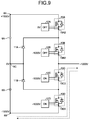
- FIG. 9 is a circuit diagram illustrating one mode of the operation of the power converter according to the third embodiment, the mode being different from that of each of FIGS. 7 and 8 .
- FIG. 9 illustrates the mode in which the semiconductor switching elements 10 A and 10 B are off, the semiconductor switching elements 10 C and 10 D are on, and the potential of the load matches the potential of the lower DC terminal 8 B.
- a current flows between the lower DC terminal 8 B and the load via the semiconductor switching elements 10 C and 10 D.
- the potential at the second main terminal 10 A 2 of the semiconductor switching element 10 A is 0 [V].
- the potential at the second main terminal 10 B 2 of the semiconductor switching element 10 B is ⁇ 1000 [V]
- the potential at the second main terminal 10 C 2 of the semiconductor switching element 10 C is ⁇ 1000 [V]
- the potential at the second main terminal 10 D 2 of the semiconductor switching element 10 D is also ⁇ 1000 [V].
- the switching operation of the semiconductor switching elements 10 A to 10 D generates a surge voltage, which is known to be particularly large when the following two operations are performed in the three-level circuit.
- a first operation refers to a case where the load receives a current, namely performs a sink operation, and is an operation in which the semiconductor switching element 10 B that is the second power semiconductor switching element performs a switching operation to cause switching of the state between the state in FIG. 8 and the state in FIG. 9 .
- a second operation refers to a case where the load discharges a current, namely performs a source operation, and is an operation in which the semiconductor switching element 10 C that is the third power semiconductor switching element performs a switching operation to cause switching of the state between the state in FIG. 7 and the state in FIG. 8 .
- These operations involve a particularly large change in the current path and are thus known to cause generation of a particularly large surge voltage.
- the description will focus on the operation in which the semiconductor switching element 10 C that is the third power semiconductor switching element performs a switching operation to cause switching of the state between the state in FIG. 7 and the state in FIG. 8 when the load discharges a current.
- a voltage of 1000 [V] identical to the capacitor voltage is applied across the impedance element group 16 in the states of FIGS. 7 and 8 .
- the detector 12 C 4 included in the third gate drive circuit 12 C detects the voltage across the impedance element group 16 .
- the gate drive circuit 12 C can thus know the voltage between the gate drive circuit 12 C and the gate drive circuit 12 D, or the capacitor voltage.
- the third gate drive circuit 12 C switches control to one that increases the driving speed for turning on and off the semiconductor switching element 10 C.
- the increase in the driving speed can prevent a turn-on switching loss and a turn-off switching loss.
- the capacitor voltage is low, so that no excessive voltage is applied to the components inside the power converter main circuit 10 .
- the third gate drive circuit 12 C switches control to one that reduces the driving speed for turning on and off the semiconductor switching element 10 C.
- the capacitor voltage is high, the decrease in the driving speed reduces the surge voltage generated at the time of switching of turn-on and turn-off to be able to prevent application of an excessive voltage to the components inside the power converter main circuit 10 .
- FIG. 10 is a circuit diagram illustrating the configuration of a main part of the power converter according to the third embodiment, the configuration being different from that of FIG. 6 .
- the characteristic of the configuration illustrated in FIG. 10 is that the impedance element group 16 is connected between the gate drive circuit 12 A that is the first gate drive circuit and the gate drive circuit 12 B that is the second gate drive circuit, and that the gate drive circuit 12 B that is the second gate drive circuit includes the detector 12 B 4 and the storage 12 B 5 . Note that the storage 12 B 5 can be omitted.
- FIG. 10 Next, the operation of the main part of the power converter illustrated in FIG. 10 will be described while focusing on the operation of the semiconductor switching element 10 B that is the second power semiconductor switching element when the load receives a current, or performs a sink operation. As for the drawings, reference is made to FIGS. 8 and 9 .
- a voltage of 1000 [V] identical to the capacitor voltage is applied to the impedance element group 16 .
- the detector 12 B 4 included in the gate drive circuit 12 B determines the magnitude relationship between the voltage across the impedance element group 16 representing the capacitor voltage information and the reference voltage, and transmits the result of the determination to the storage 12 B 5 .
- the storage 12 B 5 stores determination information as to whether the capacitor voltage is lower or higher than the reference voltage.
- the storage 12 B 5 acts on the switching speed changing unit 12 B 3 , which changes the driving speed of the semiconductor switching element 10 B on the basis of the determination information stored in the storage 12 B 5 .
- the detector 12 B 4 determines that the voltage from the impedance element group 16 is lower than the reference voltage, the result of the determination is stored in the storage 12 B 5 .
- the switching speed changing unit 12 B 3 switches control to one that increases the driving speed of the semiconductor switching element 10 B on the basis of the information determined to be lower than the reference voltage and stored in the storage 12 B 5 .
- This control prevents a switching loss of the semiconductor switching element 10 B. Note that although the above control increases the surge voltage generated at the time of switching, the capacitor voltage is low, so that no excessive voltage is applied to the components inside the power converter main circuit 10 .
- the detector 12 B 4 determines that the voltage from the impedance element group 16 is higher than the reference voltage
- the result of the determination is stored in the storage 12 B 5 .
- Information stored in the storage 12 B 5 is overwritten with a new result of the determination. That is, the latest result of the determination is stored in the storage 12 B 5 .
- the switching speed changing unit 12 B 3 switches control to one that reduces the driving speed of the semiconductor switching element 10 B on the basis of the information determined to be higher than the reference voltage and stored in the storage 12 B 5 . Although the capacitor voltage is high, this control reduces the surge voltage generated at the time of switching to be able to prevent application of an excessive voltage to the components inside the power converter main circuit 10 .
- FIG. 11 is a circuit diagram illustrating the configuration of a main part of the power converter according to the third embodiment, the configuration being different from that of each of FIGS. 6 and 10 .
- the characteristic of the configuration illustrated in FIG. 11 is that an impedance element group 18 is connected between the gate drive circuit 12 A that is the first gate drive circuit and the gate drive circuit 12 D that is the fourth gate drive circuit, the gate drive circuit 12 A that is the first gate drive circuit includes the detector 12 A 4 , and the gate drive circuit 12 D that is the fourth gate drive circuit includes a detector 12 D 4 .
- a storage can also be included as in FIG. 10 .
- the impedance element group 18 in the configuration illustrated in FIG. 11 includes impedance elements twice as many as the case of FIG. 6 , or includes ten impedance elements 18 e 1 to 18 e 10 . Note that in the state illustrated in each of FIGS. 8 and 9 , a voltage of 1000 [V] corresponding to the voltage of one capacitor is applied.
- the detectors 12 A 4 and 12 D 4 included in the gate drive circuits 12 A and 12 D, respectively, can know the capacitor voltage on the basis of voltage information or current information output from the impedance element group 18 .
- the switching speed changing unit 12 A 3 provided in the gate drive circuit 12 A performs control to switch or change the driving speed of the semiconductor switching element 10 A
- a switching speed changing unit 12 D 3 provided in the gate drive circuit 12 D performs control to switch or change the driving speed of the semiconductor switching element 10 D.
- the gate drive circuit 12 A When determining that the capacitor voltage is low, the gate drive circuit 12 A switches control to one that increases the driving speed for turning on and off the semiconductor switching element 10 A. Similarly, when determining that the capacitor voltage is low, the gate drive circuit 12 D switches control to one that increases the driving speed for turning on and off the semiconductor switching element 10 D.
- the increase in the driving speed can prevent a turn-on switching loss and a turn-off switching loss. Note that although the above control increases the surge voltage generated at the time of switching, the capacitor voltage is low, so that no excessive voltage is applied to the components inside the power converter main circuit 10 .
- the third embodiment describes the configuration as illustrated in FIGS. 6, 10 , and 11 in which a pair of two gate drive circuits is selected from the plurality of gate drive circuits and the two gate drive circuits of the pair are connected by the impedance element group 16 or 18 .
- the present invention is not limited to these configurations.
- a plurality of pairs of two gate drive circuits may be selected from the plurality of gate drive circuits and the two gate drive circuits of each pair may be connected by the impedance element group.
- the configuration as illustrated in FIG. 12 may be adopted.
- the configuration illustrated in FIG. 12 is a combination of the configurations in FIGS.
- an impedance element group 16 A including the impedance elements 16 e 1 to 16 e 5 is disposed between the gate drive circuits 12 A and 12 B
- an impedance element group 16 B including impedance elements 16 e 6 to 16 e 10 is disposed between the gate drive circuits 12 C and 12 D
- the impedance element group 18 including the impedance elements 18 e 1 to 18 e 10 is disposed between the gate drive circuits 12 A and 12 D.
- the impedance element group 16 can be disposed near the gate drive circuits 12 A and 12 B. This can shorten a path, namely electrical wiring, through which the voltage information or current information from the impedance element group 16 is transmitted to the gate drive circuits 12 A and 12 B, thereby preventing noise from being superimposed on the electrical wiring. As a result, an effect is obtained where the gate drive circuits 12 A and 12 B can change the method of driving the semiconductor switching elements 10 A and 10 B with high accuracy by using accurate voltage information or accurate current information from the impedance element group 16 .
- FIG. 13 is a circuit diagram illustrating the configuration of a main part of a power converter according to a fourth embodiment.
- FIG. 13 illustrates the load 2 to be driven, the power converter main circuit 10 that drives the load 2 ; gate drive circuits 12 UA, 12 UB, 12 VA, and 12 VB that are peripheral circuits that control the power converter main circuit 10 ; the impedance element group 16 outputting the capacitor voltage information; and the capacitor 6 that is a power supply source for the power converter main circuit 10 and accumulates DC power.
- the power converter main circuit 10 of the fourth embodiment is configured to include a semiconductor switching element 10 UA as a first U-phase power semiconductor switching element connected to the DC bus 7 A on the high potential side; a semiconductor switching element 10 UB as a second U-phase power semiconductor switching element connected to the DC bus 7 B on the low potential side; a semiconductor switching element 10 VA as a first V-phase power semiconductor switching element connected to the DC bus 7 A on the high potential side; and a semiconductor switching element 10 VB as a second V-phase power semiconductor switching element connected to the DC bus 7 B on the low potential side.
- the semiconductor switching elements 10 UA and 10 UB are connected in series, and one end of the load 2 is connected to an output terminal 5 U that is the electrical connection point of the elements.
- the semiconductor switching elements 10 VA and 10 VB are connected in series, and another end of the load 2 is connected to an output terminal 5 V that is the electrical connection point of the elements.
- the power converter main circuit 10 thus forms a single-phase inverter in which the U-phase semiconductor switching elements 10 UA and 10 UB and the V-phase semiconductor switching elements 10 VA and 10 VB are bridge-connected.
- the semiconductor switching element 10 UA is provided with a first main terminal 10 UA 1 , a second main terminal 10 UA 2 , a first signal input terminal 10 UA 3 , and a second signal input terminal 10 UA 4
- the semiconductor switching element 10 UB is provided with a first main terminal 10 UB 1 , a second main terminal 10 UB 2 , a first signal input terminal 10 UB 3 , and a second signal input terminal 10 UB 4 .
- the semiconductor switching element 10 VA is provided with a first main terminal 10 VA 1 , a second main terminal 10 VA 2 , a first signal input terminal 10 VA 3 , and a second signal input terminal 10 VA 4
- the semiconductor switching element 10 VB is provided with a first main terminal 10 VB 1 , a second main terminal 10 VB 2 , a first signal input terminal 10 VB 3 , and a second signal input terminal 10 VB 4 .
- the first main terminal 10 UA 1 of the semiconductor switching element 10 UA is connected to the DC bus 7 A
- the second main terminal 10 UB 2 of the semiconductor switching element 10 UB is connected to the DC bus 7 B
- the first main terminal 10 VA 1 of the semiconductor switching element 10 VA is connected to the DC bus 7 A
- the second main terminal 10 VB 2 of the semiconductor switching element 10 VB is connected to the DC bus 7 B.
- the DC bus 7 A is connected to the upper DC terminal 8 A of the capacitor 6
- the DC bus 7 B is connected to the lower DC terminal 8 B of the capacitor 6 . That is, the voltage of the capacitor 6 is applied between the DC buses 7 A and 7 B.
- the potential of the DC bus 7 A is applied to the load 2 when the semiconductor switching element 10 UA or 10 VA becomes conductive
- the potential of the DC bus 7 B is applied to the load 2 when the semiconductor switching element 10 UB or 10 VB becomes conductive.
- the power converter main circuit 10 thus outputs two kinds of potentials, i.e., the potential of the DC bus 7 A or the potential of the DC bus 7 B, thereby operating as a two-level, single-phase inverter circuit.
- Each of the semiconductor switching elements 10 UA, 10 UB, 10 VA, and 10 VB is formed of a transistor element and a diode element connected in parallel. Note that connection of the diode element in each of the switching elements may be omitted depending on the characteristic of the load such as when the load is a resistive load.
- FIG. 13 illustrates a MOSFET as the transistor element
- the transistor element is not limited to the MOSFET but may be any device that can switch a state between a low resistance state and a high resistance state by an electrical signal.
- an IGBT or a bipolar transistor may be used as the transistor element.
- a wide band-gap semiconductor such as SiC, GaN, or diamond in addition to Si which is used widely may be used as a material of the transistor element and the diode element making up each of the semiconductor switching elements 10 UA, 10 UB, 10 VA, and 10 VB.
- the gate drive circuit 12 UA is a first U-phase gate drive circuit that drives the semiconductor switching element 10 UA that is the first U-phase power semiconductor switching element
- the gate drive circuit 12 UB is a second U-phase gate drive circuit that drives the semiconductor switching element 10 UB that is the second U-phase power semiconductor switching element
- the gate drive circuit 12 VA is a first V-phase gate drive circuit that drives the semiconductor switching element 10 VA that is the first V-phase power semiconductor switching element
- the gate drive circuit 12 VB is a second V-phase gate drive circuit that drives the semiconductor switching element 10 VB that is the second V-phase power semiconductor switching element.
- the configuration of the gate drive circuit 12 UA is identical or equivalent to the configuration of the gate drive circuit 12 A according to the first embodiment illustrated in FIG. 1 .
- the configuration of each of the gate drive circuits 12 UB, 12 VA, and 12 VB omits a detector 12 UA 4 from the configuration of the gate drive circuit 12 UA, and is identical or equivalent to the configuration of the gate drive circuit 12 B illustrated in FIG. 4 .
- FIG. 13 omits illustration of components corresponding to the insulating circuits 14 A and 14 B and the switching signal generation unit 20 which are illustrated in FIG. 1 .
- an operating power supply for operating the detector 12 UA 4 can also be used as a power supply for driving the gate drive circuit.
- a dedicated power supply for operating the detector 12 UA 4 need not be provided if the power supply therefor is also used as the power supply for driving the gate drive circuit.
- the impedance element group 16 is connected between the gate drive circuit 12 UA that is the first U-phase gate drive circuit and the gate drive circuit 12 VA that is the first V-phase gate drive circuit. That is, FIG. 13 illustrates an example in which the impedance element group 16 is disposed between the gate drive circuits 12 UA and 12 VA belonging to different phases.
- the second main terminal 10 UA 2 and the second signal input terminal 10 UA 4 of the semiconductor switching element 10 UA have the same potential.
- the second signal input terminal 10 UA 4 of the semiconductor switching element 10 UA and one end of the impedance element group 16 are connected to the connection point of capacitors connected in series (refer to the capacitors 12 A 5 a and 12 A 5 b in the gate drive circuit 12 A in FIG. 1 ), and thus have the same potential.
- These also apply to the semiconductor switching element 10 VA. Accordingly, the voltage generated in the impedance element group 16 or the current flowing therethrough represents a potential difference between the second main terminal 10 UA 2 of the semiconductor switching element 10 UA and the second main terminal 10 VA 2 of the semiconductor switching element 10 VA.
- the gate drive circuits 12 UA and 12 VA can thus know the potential difference between the second main terminal 10 UA 2 of the semiconductor switching element 10 UA and the second main terminal 10 VA 2 of the semiconductor switching element 10 VA by detecting the voltage or the current from the impedance element group 16 .
- the impedance element group 16 can be disposed near the gate drive circuits 12 UA and 12 VA. This can shorten a path, namely electrical wiring, through which voltage information or current information from the impedance element group 16 is transmitted to the gate drive circuits 12 UA and 12 VA, thereby preventing noise from being superimposed on the electrical wiring. As a result, an effect is obtained where the gate drive circuits 12 UA and 12 VA can change the method of driving the semiconductor switching element 10 UA or 10 VA with high accuracy by using accurate voltage information or accurate current information from the impedance element group 16 .
- the operation of the power converter according to the fourth embodiment will be described with reference to FIGS. 13 to 17 as appropriate.
- the operation of the gate drive circuit will be described with reference to the gate drive circuit 12 UA including a switching speed changing unit 12 UA 3 and the detector 12 UA 4 .
- the description assumes that the voltage stored in the capacitor 6 is 1000 [V], and the negative terminal of the capacitor 6 is set as the reference potential. That is, the potential at the negative terminal of the capacitor 6 is 0 [V].
- FIG. 14 is a circuit diagram illustrating one mode of the operation of the power converter according to the fourth embodiment.
- FIG. 14 illustrates the mode in which the semiconductor switching elements 10 UA and 10 VA are on, the semiconductor switching elements 10 UB and 10 VB are off, the potential of the output terminal 5 U to which the one end of the load 2 is connected matches the potential of the upper DC terminal 8 A, and the potential of the output terminal 5 V to which the other end of the load 2 is connected also matches the potential of the upper DC terminal 8 A.
- the potential at the second main terminal 10 UA 2 of the semiconductor switching element 10 UA is +1000 [V]
- the potential at the second main terminal 10 VA 2 of the semiconductor switching element 10 VA is also +1000 [V].
- the potential at the second main terminal 10 UB 2 of the semiconductor switching element 10 UB is 0 [V]
- the potential at the second main terminal 10 VB 2 of the semiconductor switching element 10 VB is also 0 [V].
- FIG. 15 is a circuit diagram illustrating one mode of the operation of the power converter according to the fourth embodiment, the mode being different from that of FIG. 14 .
- FIG. 15 illustrates the mode in which the semiconductor switching elements 10 UA and 10 VA are off, the semiconductor switching elements 10 UB and 10 VB are on, the potential of the output terminal 5 U matches the potential of the lower DC terminal 8 B, and the potential of the output terminal 5 V also matches the potential of the lower DC terminal 8 B.
- the potential at the second main terminal 10 UA 2 of the semiconductor switching element 10 UA is 0 [V]
- the potential at the second main terminal 10 VA 2 of the semiconductor switching element 10 VA is also 0 [V].
- the potential at the second main terminal 10 UB 2 of the semiconductor switching element 10 UB is 0 [V]
- the potential at the second main terminal 10 VB 2 of the semiconductor switching element 10 VB is also 0 [V].
- FIG. 16 is a circuit diagram illustrating one mode of the operation of the power converter according to the fourth embodiment, the mode being different from that of each of FIGS. 14 and 15 .
- FIG. 16 illustrates the mode in which the semiconductor switching elements 10 UA and 10 VB are on, the semiconductor switching elements 10 UB and 10 VA are off, the potential of the output terminal 5 U matches the potential of the upper DC terminal 8 A, and the potential of the output terminal 5 V matches the potential of the lower DC terminal 8 B.
- the potential at the second main terminal 10 UA 2 of the semiconductor switching element 10 UA is +1000 [V]
- the potential at the second main terminal 10 VA 2 of the semiconductor switching element 10 VA is 0 [V].
- the potential at the second main terminal 10 UB 2 of the semiconductor switching element 10 UB is 0 [V]
- the potential at the second main terminal 10 VB 2 of the semiconductor switching element 10 VB is also 0 [V].
- FIG. 17 is a circuit diagram illustrating one mode of the operation of the power converter according to the fourth embodiment, the mode being different from that of each of FIGS. 14 to 16 .
- FIG. 17 illustrates the mode in which the semiconductor switching elements 10 UA and 10 VB are off, the semiconductor switching elements 10 UB and 10 VA are on, the potential of the output terminal 5 U matches the potential of the lower DC terminal 8 B, and the potential of the output terminal 5 V matches the potential of the upper DC terminal 8 A.
- the potential at the second main terminal 10 UA 2 of the semiconductor switching element 10 UA is 0 [V]
- the potential at the second main terminal 10 VA 2 of the semiconductor switching element 10 VA is +1000 [V].
- the potential at the second main terminal 10 UB 2 of the semiconductor switching element 10 UB is 0 [V]
- the potential at the second main terminal 10 VB 2 of the semiconductor switching element 10 VB is also 0 [V].
- a voltage of 1000 [V] identical to the capacitor voltage is applied to the impedance element group 16 .
- the detector 12 UA 4 included in the gate drive circuit 12 UA determines the magnitude relationship between the voltage across the impedance element group 16 representing the capacitor voltage information and the reference voltage, and transmits the result of the determination to the switching speed changing unit 12 UA 3 .
- the switching speed changing unit 12 UA 3 can determine whether the capacitor voltage is lower or higher than the reference voltage on the basis of the result of the determination.
- the switching speed changing unit 12 UA 3 switches control to one that increases the driving speed of the semiconductor switching element 10 UA. This control prevents a switching loss of the semiconductor switching element 10 UA. Note that although the above control increases the surge voltage generated at the time of switching, the capacitor voltage is low, so that no excessive voltage is applied to the components inside the power converter main circuit 10 . The transition is thus made between the state of FIG. 16 and the state of FIG. 15 , and between the state of FIG. 17 and the state of FIG. 14 .
- the switching speed changing unit 12 UA 3 switches control to one that reduces the driving speed of the semiconductor switching element 10 UA. Although the capacitor voltage is high, this control reduces the surge voltage generated at the time of switching to be able to prevent application of an excessive voltage to the components inside the power converter main circuit 10 .
- FIG. 18 is a circuit diagram illustrating the configuration of a main part of the power converter according to the fourth embodiment, the configuration being different from that of FIG. 13 and including a storage 12 UA 5 in the gate drive circuit 12 UA.
- a voltage of 1000 [V] identical to the capacitor voltage is applied to the impedance element group 16 .
- the detector 12 UA 4 determines the magnitude relationship between the voltage from the impedance element group 16 and the reference voltage. When the detector 12 UA 4 determines that the voltage from the impedance element group 16 is lower than the reference voltage, the result of the determination is stored in the storage 12 UA 5 .
- the switching speed changing unit 12 UA 3 switches control to one that increases the driving speed of the semiconductor switching element 10 UA on the basis of the information determined to be lower than the reference voltage and stored in the storage 12 UA 5 .
- This control prevents a switching loss of the semiconductor switching element 10 UA. Note that although the above control increases the surge voltage generated at the time of switching, the capacitor voltage is low, so that no excessive voltage is applied to the components inside the power converter main circuit 10 . The transition is thus made between the state of FIG. 16 and the state of FIG. 15 , and between the state of FIG. 17 and the state of FIG. 14 .
- the detector 12 UA 4 determines that the voltage from the impedance element group 16 is higher than the reference voltage, the result of the determination is stored in the storage 12 UA 5 .
- Information stored in the storage 12 UA 5 is overwritten with a new result of the determination. That is, the latest result of the determination is stored in the storage 12 UA 5 .
- the switching speed changing unit 12 UA 3 switches control to one that reduces the driving speed of the semiconductor switching element 10 UA on the basis of the information determined to be higher than the reference voltage and stored in the storage 12 UA 5 . Although the capacitor voltage is high, this control reduces the surge voltage generated at the time of switching to be able to prevent application of an excessive voltage to the components inside the power converter main circuit 10 .
- FIG. 13 illustrates the configuration in which the detector 12 UA 4 is provided only in the gate drive circuit 12 UA that is the first U-phase gate drive circuit
- the detector may also be provided in the gate drive circuit 12 VA that is the first V-phase gate drive circuit.
- This configuration allows the gate drive circuit 12 VA to change the method of driving the semiconductor switching element 10 VA that is the first V-phase power semiconductor switching element on the basis of output of the detector.
- a storage may be provided in the gate drive circuit 12 VA as in FIG. 18 , whereby the effect similar to that of the second and third embodiments can be obtained.
- FIG. 19 is a circuit diagram illustrating the configuration of a main part of the power converter according to the fourth embodiment, the configuration being different from that of each of FIGS. 13 and 18 .
- the characteristic of the configuration illustrated in FIG. 19 is that two impedance element groups 16 U and 16 V are included as impedance element groups, the first impedance element group 16 U is connected between the gate drive circuit 12 UA that is the first U-phase gate drive circuit and the gate drive circuit 12 UB that is the second U-phase gate drive circuit, the second impedance element group 16 V is connected between the gate drive circuit 12 VA that is the first V-phase gate drive circuit and the gate drive circuit 12 UB that is the second U-phase gate drive circuit, and the gate drive circuit 12 UB is provided with a second detector 12 UB 4 b that detects a voltage or current across the first impedance element group 16 U and a first detector 12 UB 4 a that detects a voltage or current across the second impedance element group 16 V.
- the first detector 12 UB 4 a provided in the gate drive circuit 12 UB can transmit, to a switching speed changing unit 12 UB 3 , capacitor voltage information that is obtained from voltage information or current information output from the first impedance element group 16 U.
- the second detector 12 UB 4 b provided in the gate drive circuit 12 UB can transmit, to the switching speed changing unit 12 UB 3 , capacitor voltage information that is obtained from voltage information or current information output from the second impedance element group 16 V.
- the switching speed changing unit 12 UB 3 can perform control to switch or change the driving speed of the semiconductor switching element 10 UB. Note that the control for switching the driving speed is as described above, and thus will not be described in detail.
- the opportunity to obtain the capacitor voltage information increases in the switching cycle in which the semiconductor switching elements 10 UA, 10 UB, 10 VA, and 10 VB making up the power converter main circuit 10 are turned on or off, whereby an effect is obtained where the method of driving the semiconductor switching element 10 UB can be changed with higher accuracy than the configurations described in the first to third embodiments.
Landscapes
- Engineering & Computer Science (AREA)
- Power Engineering (AREA)
- Physics & Mathematics (AREA)
- Electromagnetism (AREA)
- Power Conversion In General (AREA)
- Inverter Devices (AREA)
Abstract
Description
Claims (10)
Applications Claiming Priority (1)
| Application Number | Priority Date | Filing Date | Title |
|---|---|---|---|
| PCT/JP2015/075070 WO2017037916A1 (en) | 2015-09-03 | 2015-09-03 | Power conversion device |
Publications (2)
| Publication Number | Publication Date |
|---|---|
| US20190006934A1 US20190006934A1 (en) | 2019-01-03 |
| US10727729B2 true US10727729B2 (en) | 2020-07-28 |
Family
ID=58186757
Family Applications (1)
| Application Number | Title | Priority Date | Filing Date |
|---|---|---|---|
| US15/745,265 Active US10727729B2 (en) | 2015-09-03 | 2015-09-03 | Power converter |
Country Status (5)
| Country | Link |
|---|---|
| US (1) | US10727729B2 (en) |
| JP (1) | JP6261828B2 (en) |
| CN (1) | CN107925352B (en) |
| DE (1) | DE112015006875T5 (en) |
| WO (1) | WO2017037916A1 (en) |
Cited By (1)
| Publication number | Priority date | Publication date | Assignee | Title |
|---|---|---|---|---|
| US11831232B2 (en) | 2021-08-13 | 2023-11-28 | General Electric Company | Power converter having a gate drive circuit and method of operating |
Families Citing this family (5)
| Publication number | Priority date | Publication date | Assignee | Title |
|---|---|---|---|---|
| JP6128201B1 (en) * | 2015-12-28 | 2017-05-17 | ダイキン工業株式会社 | Power supply device, inverter device using the power supply device, converter device, refrigeration device using the inverter device or converter device, and air purifier |
| CN109951058A (en) * | 2017-12-21 | 2019-06-28 | 维谛公司 | A kind of method and device for the switching loss reducing switching tube |
| JP7198028B2 (en) * | 2018-10-01 | 2022-12-28 | ローム株式会社 | Driver device |
| CN110380599B (en) * | 2019-08-07 | 2020-11-27 | 电子科技大学 | Mixed type grid drive circuit |
| JP2022124831A (en) * | 2021-02-16 | 2022-08-26 | オムロン株式会社 | Power converting device and control method |
Citations (14)
| Publication number | Priority date | Publication date | Assignee | Title |
|---|---|---|---|---|
| JPH06291631A (en) | 1993-03-31 | 1994-10-18 | Hitachi Ltd | Method and circuit for driving voltage driven element |
| JPH0923664A (en) | 1995-07-07 | 1997-01-21 | Nippondenso Co Ltd | Inverter device |
| JP2003079129A (en) | 2001-09-04 | 2003-03-14 | Hitachi Ltd | Gate drive circuit and power converter using the same |
| US20030156439A1 (en) | 2002-02-18 | 2003-08-21 | Mitsubishi Denki Kabushiki Kaisha | Drive circuit |
| US20050128671A1 (en) | 2003-12-10 | 2005-06-16 | Mitsubishi Denki Kabushiki Kaisha | Control device of switching device and control device of driving circuit of motor |
| US20050146295A1 (en) | 2004-01-07 | 2005-07-07 | Mitsubishi Denki Kabushiki Kaisha | Booster and motor controller |
| JP2008154420A (en) | 2006-12-20 | 2008-07-03 | Toshiba Mitsubishi-Electric Industrial System Corp | Power conversion device |
| WO2014128842A1 (en) | 2013-02-20 | 2014-08-28 | 株式会社 日立製作所 | Power converter |
| JP2015023642A (en) | 2013-07-18 | 2015-02-02 | 株式会社日立製作所 | Inverter device |
| JP2015023776A (en) | 2013-07-24 | 2015-02-02 | 三菱電機株式会社 | Power conversion circuit and control method thereof |
| US20150145586A1 (en) * | 2013-11-26 | 2015-05-28 | Samsung Electro-Mechanics Co., Ltd. | Gate driving device and inverter having the same |
| WO2015097836A1 (en) | 2013-12-27 | 2015-07-02 | 株式会社日立産機システム | Power conversion device and power conversion device control method |
| US20160112043A1 (en) * | 2013-06-11 | 2016-04-21 | Rohm Co., Ltd. | Electronic circuit |
| US20160352321A1 (en) * | 2014-02-14 | 2016-12-01 | Rohm Co., Ltd. | Gate drive circuit and power supply |
Family Cites Families (2)
| Publication number | Priority date | Publication date | Assignee | Title |
|---|---|---|---|---|
| US6979980B1 (en) * | 2004-08-24 | 2005-12-27 | Advanced Energy Industries, Inc. | Soft switching interleaved power converter |
| JP5751066B2 (en) * | 2011-07-26 | 2015-07-22 | 横河電機株式会社 | Power supply device and dual power supply device using the same |
-
2015
- 2015-09-03 CN CN201580082652.7A patent/CN107925352B/en active Active
- 2015-09-03 DE DE112015006875.9T patent/DE112015006875T5/en active Pending
- 2015-09-03 JP JP2017534767A patent/JP6261828B2/en active Active
- 2015-09-03 US US15/745,265 patent/US10727729B2/en active Active
- 2015-09-03 WO PCT/JP2015/075070 patent/WO2017037916A1/en active Application Filing
Patent Citations (19)
| Publication number | Priority date | Publication date | Assignee | Title |
|---|---|---|---|---|
| JPH06291631A (en) | 1993-03-31 | 1994-10-18 | Hitachi Ltd | Method and circuit for driving voltage driven element |
| JPH0923664A (en) | 1995-07-07 | 1997-01-21 | Nippondenso Co Ltd | Inverter device |
| JP2003079129A (en) | 2001-09-04 | 2003-03-14 | Hitachi Ltd | Gate drive circuit and power converter using the same |
| US20030156439A1 (en) | 2002-02-18 | 2003-08-21 | Mitsubishi Denki Kabushiki Kaisha | Drive circuit |
| JP2003244966A (en) | 2002-02-18 | 2003-08-29 | Mitsubishi Electric Corp | Drive circuit |
| US20050128671A1 (en) | 2003-12-10 | 2005-06-16 | Mitsubishi Denki Kabushiki Kaisha | Control device of switching device and control device of driving circuit of motor |
| JP2005175741A (en) | 2003-12-10 | 2005-06-30 | Mitsubishi Electric Corp | Controller of switching device, and control unit of drive circuit of motor |
| JP2005198406A (en) | 2004-01-07 | 2005-07-21 | Mitsubishi Electric Corp | Step-up device and motor controller |
| US20050146295A1 (en) | 2004-01-07 | 2005-07-07 | Mitsubishi Denki Kabushiki Kaisha | Booster and motor controller |
| JP2008154420A (en) | 2006-12-20 | 2008-07-03 | Toshiba Mitsubishi-Electric Industrial System Corp | Power conversion device |
| WO2014128842A1 (en) | 2013-02-20 | 2014-08-28 | 株式会社 日立製作所 | Power converter |
| US20160006368A1 (en) | 2013-02-20 | 2016-01-07 | Hitachi, Ltd. | Power Converter |
| US20160112043A1 (en) * | 2013-06-11 | 2016-04-21 | Rohm Co., Ltd. | Electronic circuit |
| JP2015023642A (en) | 2013-07-18 | 2015-02-02 | 株式会社日立製作所 | Inverter device |
| JP2015023776A (en) | 2013-07-24 | 2015-02-02 | 三菱電機株式会社 | Power conversion circuit and control method thereof |
| US20150145586A1 (en) * | 2013-11-26 | 2015-05-28 | Samsung Electro-Mechanics Co., Ltd. | Gate driving device and inverter having the same |
| WO2015097836A1 (en) | 2013-12-27 | 2015-07-02 | 株式会社日立産機システム | Power conversion device and power conversion device control method |
| EP3089346A1 (en) | 2013-12-27 | 2016-11-02 | Hitachi Industrial Equipment Systems Co., Ltd. | Power conversion device and power conversion device control method |
| US20160352321A1 (en) * | 2014-02-14 | 2016-12-01 | Rohm Co., Ltd. | Gate drive circuit and power supply |
Non-Patent Citations (5)
| Title |
|---|
| International Search Report (PCT/ISA/210) dated Nov. 24, 2015, by the Japanese Patent Office as the International Searching Authority for International Application No. PCT/JP2015/075070. |
| Notification of Reason for Refusal for Japanese Patent Application No. 2017-534767 dated Aug. 25, 2017. |
| Office Action dated Oct. 17, 2019, by the India Patent Office in corresponding India Patent Application No. 201847005535 and English translation of the Office Action. (5 pages). |
| Office Action dated Oct. 9, 2019, by the Chinese Patent Office in corresponding Chinese Patent Application No. 201580082652.7 and English translation of the Office Action. (9 pages). |
| Written Opinion (PCT/ISA/237) dated Nov. 24, 2015, by the Japanese Patent Office as the International Searching Authority for International Application No. PCT/JP2015/075070. |
Cited By (1)
| Publication number | Priority date | Publication date | Assignee | Title |
|---|---|---|---|---|
| US11831232B2 (en) | 2021-08-13 | 2023-11-28 | General Electric Company | Power converter having a gate drive circuit and method of operating |
Also Published As
| Publication number | Publication date |
|---|---|
| CN107925352A (en) | 2018-04-17 |
| US20190006934A1 (en) | 2019-01-03 |
| CN107925352B (en) | 2020-11-03 |
| JP6261828B2 (en) | 2018-01-17 |
| JPWO2017037916A1 (en) | 2017-09-21 |
| DE112015006875T5 (en) | 2018-05-17 |
| WO2017037916A1 (en) | 2017-03-09 |
Similar Documents
| Publication | Publication Date | Title |
|---|---|---|
| US10727729B2 (en) | Power converter | |
| US11139808B2 (en) | Semiconductor device and power conversion system | |
| US9874614B2 (en) | Semiconductor apparatus and power conversion apparatus | |
| US9112344B2 (en) | Driver for switching element and control system for rotary machine using the same | |
| US9106155B2 (en) | Three-level power conversion circuit system | |
| JP6040582B2 (en) | Protection control method for multi-level power conversion circuit | |
| US11183835B2 (en) | Short circuit detection and protection for a gate driver circuit and methods of detecting the same using logic analysis | |
| EP2953258B1 (en) | Tnpc inverter device and method for detecting short-circuit thereof | |
| US9214873B2 (en) | Method for operating an electrical power rectifier, as well as an electrical power rectifier | |
| US9300198B2 (en) | Semiconductor device, including temperature sensing circut | |
| US20210057997A1 (en) | Power supply device | |
| JP2016005289A (en) | Power conversion device having deterioration diagnosis function | |
| JP2018007403A (en) | Power converter | |
| JP2019527027A (en) | Current converter driving method and current converter driven by the method | |
| WO2015064206A1 (en) | Semiconductor device | |
| JP2019176587A (en) | Dc/dc converter | |
| JP2010035284A (en) | Overcurrent protection circuit | |
| CN111527684A (en) | Power module with built-in driving circuit | |
| US20130193762A1 (en) | Three-level power converting apparatus | |
| CN111106742B (en) | Driving circuit for switch | |
| JP2019030081A (en) | Power conversion apparatus and failure diagnosis method | |
| CN112640276B (en) | Driving circuit of switch | |
| JP2015119594A (en) | Drive control device of semiconductor device | |
| JP2014155311A (en) | Protection circuit | |
| JP2019047698A (en) | Semiconductor device |
Legal Events
| Date | Code | Title | Description |
|---|---|---|---|
| AS | Assignment |
Owner name: MITSUBISHI ELECTRIC CORPORATION, JAPAN Free format text: ASSIGNMENT OF ASSIGNORS INTEREST;ASSIGNORS:NAKASHIMA, YUKIO;MIKI, TAKAYOSHI;SIGNING DATES FROM 20171201 TO 20171205;REEL/FRAME:044629/0215 |
|
| FEPP | Fee payment procedure |
Free format text: ENTITY STATUS SET TO UNDISCOUNTED (ORIGINAL EVENT CODE: BIG.); ENTITY STATUS OF PATENT OWNER: LARGE ENTITY |
|
| STPP | Information on status: patent application and granting procedure in general |
Free format text: RESPONSE TO NON-FINAL OFFICE ACTION ENTERED AND FORWARDED TO EXAMINER |
|
| STPP | Information on status: patent application and granting procedure in general |
Free format text: NON FINAL ACTION MAILED |
|
| STPP | Information on status: patent application and granting procedure in general |
Free format text: RESPONSE TO NON-FINAL OFFICE ACTION ENTERED AND FORWARDED TO EXAMINER |
|
| STPP | Information on status: patent application and granting procedure in general |
Free format text: NOTICE OF ALLOWANCE MAILED -- APPLICATION RECEIVED IN OFFICE OF PUBLICATIONS |
|
| STPP | Information on status: patent application and granting procedure in general |
Free format text: NOTICE OF ALLOWANCE MAILED -- APPLICATION RECEIVED IN OFFICE OF PUBLICATIONS |
|
| STPP | Information on status: patent application and granting procedure in general |
Free format text: PUBLICATIONS -- ISSUE FEE PAYMENT VERIFIED |
|
| STCF | Information on status: patent grant |
Free format text: PATENTED CASE |
|
| MAFP | Maintenance fee payment |
Free format text: PAYMENT OF MAINTENANCE FEE, 4TH YEAR, LARGE ENTITY (ORIGINAL EVENT CODE: M1551); ENTITY STATUS OF PATENT OWNER: LARGE ENTITY Year of fee payment: 4 |