US10713451B2 - Optical jumper - Google Patents
Optical jumper Download PDFInfo
- Publication number
- US10713451B2 US10713451B2 US15/746,672 US201515746672A US10713451B2 US 10713451 B2 US10713451 B2 US 10713451B2 US 201515746672 A US201515746672 A US 201515746672A US 10713451 B2 US10713451 B2 US 10713451B2
- Authority
- US
- United States
- Prior art keywords
- optical
- tag
- connector
- jumper
- optical jumper
- Prior art date
- Legal status (The legal status is an assumption and is not a legal conclusion. Google has not performed a legal analysis and makes no representation as to the accuracy of the status listed.)
- Active, expires
Links
- 230000003287 optical effect Effects 0.000 title claims abstract description 387
- 239000000835 fiber Substances 0.000 claims description 16
- 238000009434 installation Methods 0.000 claims description 10
- 238000000034 method Methods 0.000 claims description 9
- 238000004519 manufacturing process Methods 0.000 claims description 8
- 230000008878 coupling Effects 0.000 claims description 4
- 238000010168 coupling process Methods 0.000 claims description 4
- 238000005859 coupling reaction Methods 0.000 claims description 4
- 238000003491 array Methods 0.000 description 35
- 239000000758 substrate Substances 0.000 description 29
- 101100481015 Caenorhabditis elegans tag-278 gene Proteins 0.000 description 7
- 239000013307 optical fiber Substances 0.000 description 7
- RYGMFSIKBFXOCR-UHFFFAOYSA-N Copper Chemical compound [Cu] RYGMFSIKBFXOCR-UHFFFAOYSA-N 0.000 description 2
- 238000010586 diagram Methods 0.000 description 2
- 230000006978 adaptation Effects 0.000 description 1
- 229910052802 copper Inorganic materials 0.000 description 1
- 239000010949 copper Substances 0.000 description 1
- 230000006870 function Effects 0.000 description 1
- 230000014759 maintenance of location Effects 0.000 description 1
- 230000013011 mating Effects 0.000 description 1
- 230000008439 repair process Effects 0.000 description 1
Images


Classifications
-
- G—PHYSICS
- G06—COMPUTING; CALCULATING OR COUNTING
- G06K—GRAPHICAL DATA READING; PRESENTATION OF DATA; RECORD CARRIERS; HANDLING RECORD CARRIERS
- G06K7/00—Methods or arrangements for sensing record carriers, e.g. for reading patterns
- G06K7/10—Methods or arrangements for sensing record carriers, e.g. for reading patterns by electromagnetic radiation, e.g. optical sensing; by corpuscular radiation
- G06K7/10009—Methods or arrangements for sensing record carriers, e.g. for reading patterns by electromagnetic radiation, e.g. optical sensing; by corpuscular radiation sensing by radiation using wavelengths larger than 0.1 mm, e.g. radio-waves or microwaves
- G06K7/10366—Methods or arrangements for sensing record carriers, e.g. for reading patterns by electromagnetic radiation, e.g. optical sensing; by corpuscular radiation sensing by radiation using wavelengths larger than 0.1 mm, e.g. radio-waves or microwaves the interrogation device being adapted for miscellaneous applications
-
- G—PHYSICS
- G02—OPTICS
- G02B—OPTICAL ELEMENTS, SYSTEMS OR APPARATUS
- G02B6/00—Light guides; Structural details of arrangements comprising light guides and other optical elements, e.g. couplings
- G02B6/24—Coupling light guides
- G02B6/42—Coupling light guides with opto-electronic elements
- G02B6/4201—Packages, e.g. shape, construction, internal or external details
- G02B6/4285—Optical modules characterised by a connectorised pigtail
-
- G—PHYSICS
- G02—OPTICS
- G02B—OPTICAL ELEMENTS, SYSTEMS OR APPARATUS
- G02B6/00—Light guides; Structural details of arrangements comprising light guides and other optical elements, e.g. couplings
- G02B6/24—Coupling light guides
- G02B6/36—Mechanical coupling means
- G02B6/38—Mechanical coupling means having fibre to fibre mating means
- G02B6/3807—Dismountable connectors, i.e. comprising plugs
- G02B6/3895—Dismountable connectors, i.e. comprising plugs identification of connection, e.g. right plug to the right socket or full engagement of the mating parts
-
- G—PHYSICS
- G02—OPTICS
- G02B—OPTICAL ELEMENTS, SYSTEMS OR APPARATUS
- G02B6/00—Light guides; Structural details of arrangements comprising light guides and other optical elements, e.g. couplings
- G02B6/24—Coupling light guides
- G02B6/42—Coupling light guides with opto-electronic elements
- G02B6/4201—Packages, e.g. shape, construction, internal or external details
-
- G—PHYSICS
- G02—OPTICS
- G02B—OPTICAL ELEMENTS, SYSTEMS OR APPARATUS
- G02B6/00—Light guides; Structural details of arrangements comprising light guides and other optical elements, e.g. couplings
- G02B6/24—Coupling light guides
- G02B6/42—Coupling light guides with opto-electronic elements
- G02B6/4292—Coupling light guides with opto-electronic elements the light guide being disconnectable from the opto-electronic element, e.g. mutually self aligning arrangements
- G02B6/4293—Coupling light guides with opto-electronic elements the light guide being disconnectable from the opto-electronic element, e.g. mutually self aligning arrangements hybrid electrical and optical connections for transmitting electrical and optical signals
-
- G—PHYSICS
- G02—OPTICS
- G02B—OPTICAL ELEMENTS, SYSTEMS OR APPARATUS
- G02B6/00—Light guides; Structural details of arrangements comprising light guides and other optical elements, e.g. couplings
- G02B6/44—Mechanical structures for providing tensile strength and external protection for fibres, e.g. optical transmission cables
- G02B6/4439—Auxiliary devices
-
- G—PHYSICS
- G06—COMPUTING; CALCULATING OR COUNTING
- G06K—GRAPHICAL DATA READING; PRESENTATION OF DATA; RECORD CARRIERS; HANDLING RECORD CARRIERS
- G06K19/00—Record carriers for use with machines and with at least a part designed to carry digital markings
- G06K19/06—Record carriers for use with machines and with at least a part designed to carry digital markings characterised by the kind of the digital marking, e.g. shape, nature, code
- G06K19/067—Record carriers with conductive marks, printed circuits or semiconductor circuit elements, e.g. credit or identity cards also with resonating or responding marks without active components
- G06K19/07—Record carriers with conductive marks, printed circuits or semiconductor circuit elements, e.g. credit or identity cards also with resonating or responding marks without active components with integrated circuit chips
- G06K19/0723—Record carriers with conductive marks, printed circuits or semiconductor circuit elements, e.g. credit or identity cards also with resonating or responding marks without active components with integrated circuit chips the record carrier comprising an arrangement for non-contact communication, e.g. wireless communication circuits on transponder cards, non-contact smart cards or RFIDs
-
- G—PHYSICS
- G06—COMPUTING; CALCULATING OR COUNTING
- G06K—GRAPHICAL DATA READING; PRESENTATION OF DATA; RECORD CARRIERS; HANDLING RECORD CARRIERS
- G06K7/00—Methods or arrangements for sensing record carriers, e.g. for reading patterns
- G06K7/10—Methods or arrangements for sensing record carriers, e.g. for reading patterns by electromagnetic radiation, e.g. optical sensing; by corpuscular radiation
- G06K7/10009—Methods or arrangements for sensing record carriers, e.g. for reading patterns by electromagnetic radiation, e.g. optical sensing; by corpuscular radiation sensing by radiation using wavelengths larger than 0.1 mm, e.g. radio-waves or microwaves
- G06K7/10297—Methods or arrangements for sensing record carriers, e.g. for reading patterns by electromagnetic radiation, e.g. optical sensing; by corpuscular radiation sensing by radiation using wavelengths larger than 0.1 mm, e.g. radio-waves or microwaves arrangements for handling protocols designed for non-contact record carriers such as RFIDs NFCs, e.g. ISO/IEC 14443 and 18092
-
- G—PHYSICS
- G02—OPTICS
- G02B—OPTICAL ELEMENTS, SYSTEMS OR APPARATUS
- G02B6/00—Light guides; Structural details of arrangements comprising light guides and other optical elements, e.g. couplings
- G02B6/24—Coupling light guides
- G02B6/42—Coupling light guides with opto-electronic elements
- G02B6/4201—Packages, e.g. shape, construction, internal or external details
- G02B6/4274—Electrical aspects
- G02B6/4284—Electrical aspects of optical modules with disconnectable electrical connectors
-
- H—ELECTRICITY
- H04—ELECTRIC COMMUNICATION TECHNIQUE
- H04B—TRANSMISSION
- H04B10/00—Transmission systems employing electromagnetic waves other than radio-waves, e.g. infrared, visible or ultraviolet light, or employing corpuscular radiation, e.g. quantum communication
- H04B10/40—Transceivers
Definitions
- An optical jumper includes an optical cable, a near-end connector optically coupled to one end of the optical cable, and a far-end connector optically coupled to the other end of the optical cable.
- the configuration of the optical jumper may vary based on, for example, the length and type of the optical cable and the connector types.
- FIGS. 1A and 1B illustrate examples of an optical jumper.
- FIG. 2 illustrates one example of a system including an optical transceiver module.
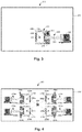
- FIG. 3 illustrates a top view of one example of a system with an optical jumper installed.
- FIG. 4 illustrates a top view of another example of a system with a plurality of optical jumpers installed.
- FIGS. 5A and 5B illustrate various views of one example of an optical transceiver module and an optical jumper.
- FIGS. 6A-6D illustrate various views of another example of an optical transceiver module and an optical jumper.
- FIGS. 7A-7E illustrate various views of another example of an optical transceiver module and an optical jumper.
- FIGS. 8A and 8B illustrate various views of another example of an optical transceiver module and an optical jumper.
- FIG. 9 is a flow diagram illustrating one example of a method for configuring an optical transceiver.
- the settings of the optical transceiver are non-programmatically configured differently based on the configuration of the optical jumper installed.
- the optical transceiver may also be non-programmatically configured to turn on or turn off portions of the optical transceiver based on the configuration of the optical jumper installed.
- Non-programmatically adjusting optical transceiver settings of multiple optical transceivers with different optical jumpers for different applications and/or installations may be an error-prone process.
- One example to non-programmatically configuring or adjusting an optical transceiver is manually configuring or adjusting the optical transceiver.
- an optical jumper for installation in a system including an optical transceiver and a tag reader.
- the optical jumper includes an optical cable, a near-end (i.e., first) connector optically coupled to a first end of the optical cable for connecting to the optical transceiver, a far-end (i.e., second) connector optically coupled to a second end of the optical cable, and a tag coupled to the near-end connector.
- the tag is readable by the tag reader of the system when the optical jumper is coupled to the optical transceiver of the system.
- the tag stores data identifying the optical cable, the near-end connector, and the far-end connector so that the system can automatically configure the optical transceiver based on the stored data.
- FIG. 1A illustrates one example of an optical jumper 100 a .
- Optical jumper 100 a includes a near-end (i.e., first) connector 102 , an optical cable 104 a , and a far-end (i.e., second) connector 106 .
- Near-end connector 102 is optically coupled to one end of optical cable 104 a
- far-end connector 106 is optically coupled to the other end of optical cable 104 a .
- Optical cable 104 a includes any suitable number of optical fibers to optically couple near-end connector 102 to far-end connector 106 .
- Near-end connector 102 may include an optical lens block 108 . In other examples, optical lens block 108 may be excluded.
- Near-end connector 102 may be a MT connector, a Prism LT connector, a Prism MT connector, or another suitable connector.
- Far-end connector 106 may be a MT connector, a Multi-fiber Push-On (MPO) connector, a Lucent Connecter (LC), or another suitable connector.
- MPO Multi-fiber Push-On
- LC Lucent Connecter
- Far-end connector 106 may be installed on a faceplate of a system or connected to another optical transceiver in a system.
- Optical jumper 100 a also includes a tag 110 coupled to near-end connector 102 .
- Tag 110 includes a non-volatile memory and control logic for accessing the non-volatile memory and for communicating with a tag reader or tag reader/writer of a system.
- the control logic may include a wireless interface (e.g., Radio Frequency Identification (RFID) interface or Near Field Communication (NFC) interface) or a wired interface (e.g., I 2 C) to communicate with a tag reader or tag reader/writer of a system when optical jumper 110 a is installed in a system.
- RFID Radio Frequency Identification
- NFC Near Field Communication
- Tag 110 stores data identifying optical jumper 100 a including near-end connector 102 , optical cable 104 a , and far-end connector 106 .
- tag 110 is programmed with the data when optical jumper 100 a is assembled.
- the data may identify, for example, at least one of a connector type of near-end connector 102 , an optical loss of near-end connector 102 , a ferrule lens or physical contact type of near-end connector 102 , a number of fiber positions of near-end connector 102 , a fiber configuration of near end connector 102 , a fiber type of optical cable 104 a , a length of optical cable 104 a , a connector type of far-end connector 106 , an optical loss of far-end connector 106 , a ferrule lens or physical contact type of far-end connector 106 , a number of fiber positions of far-end connector 106 , a fiber configuration of far-end connector 106 , a manufacturer of optical jumper 100 a , a
- FIG. 1B illustrates another example of an optical jumper 100 b .
- Optical jumper 100 b includes a near-end (i.e., first) connector 102 , an optical cable 104 b , and a plurality of far-end (i.e., second) connectors 106 a and 106 b . While optical jumper 100 b as illustrated in FIG. 1B includes two far-end connectors, in other examples optical jumper 100 b may include any suitable number of far-end connectors.
- optical cable 104 b is a breakout cable.
- Near-end connector 102 is optically coupled to one end of optical cable 104 b , and each far-end connector 106 a and 106 b is optically coupled to the other end of optical cable 104 b .
- Optical cable 104 b includes any suitable number of optical fibers to optically couple near-end connector 102 to each far-end connector 106 a and 106 b .
- Near-end connector 102 may include an optical lens block 108 . In other examples, optical lens block 108 may be excluded.
- Each far-end connector 106 a and 106 b may be a MT connector, a MPO connector, a LC connector, or another suitable connector.
- Each far-end connector 106 a and 106 b may be installed on a faceplate of a system or connected to an optical transceiver.
- Optical jumper 100 b also includes a tag 110 coupled to near-end connector 102 as previously described with reference to FIG. 1A .
- tag 110 may also store the number of far-end connectors, the connector type of each far-end connector 106 a and 106 b , the optical loss of each far-end connector 106 a and 106 b , the ferrule lens or physical contact type of each far-end connector 106 a and 106 b , the number of fiber positions of each far-end connector 106 a and 106 b , and the fiber configuration of each far-end connector 106 a and 106 b .
- the data may identify other attributes of optical jumper 100 b.
- FIG. 2 illustrates one example of a system 150 including an optical transceiver module 152 .
- System 150 includes a system board 154 (i.e., Printed Circuit Board (PCB)) and a management controller 156 electrically coupled to system board 154 .
- Optical transceiver module 152 includes an optical transceiver substrate (e.g., PCB) 160 electrically coupled to system board 154 , laser and PIN detector arrays 162 , an optical jumper socket 164 , a modulator integrated circuit (IC) 166 , a management controller 168 , and a tag reader/writer 170 .
- the term “tag reader/writer” as used herein may refer to either a tag reader or a tag reader and writer.
- Management controller 156 is communicatively coupled to management controller 168 via system board 154 and optical transceiver substrate 160 .
- Management controller 156 and management controller 168 exchange optical transceiver configuration and status information.
- Laser and PIN detector arrays 162 , modulator IC 166 , and tag reader/writer 170 are each electrically coupled to optical transceiver substrate 160 and may be electrically coupled to each other via optical transceiver substrate 160 .
- tag reader/writer 170 is mounted on and electrically coupled to system board 154 .
- Optical jumper socket 164 is mechanically coupled to optical transceiver substrate 160 over laser and PIN detector arrays 162 .
- Optical jumper socket 164 receives a near-end connector of an optical jumper, such as near-end connector 102 of optical jumper 100 a or 100 b previously described with reference to FIGS. 1A and 1B , to mechanically and optically couple optical transceiver module 152 to the optical jumper.
- Tag reader/writer 170 reads the data stored in the tag of an optical jumper, such as tag 110 of optical jumper 100 a or 100 b previously described with reference to FIGS. 1A and 1B , when the optical jumper is coupled to optical transceiver module 152 .
- Tag reader/writer 170 includes a wireless interface (e.g., RFID interface or NFC interface) or a wired interface (e.g., I 2 C) to communicate with a tag of an optical jumper when the optical jumper is coupled to optical transceiver module 152 .
- tag reader/writer 170 communicates the data read from the tag directly to modulator IC 166 .
- tag reader/writer 170 communicates the data read from the tag to management controller 168 , which in turn communicates the data to modulator IC 166 .
- Modulator IC 166 configures itself and laser and PIN detector arrays 162 based on the data.
- optical power levels are configured and portions of the modulator IC 166 and laser and PIN detector arrays 162 are either activated or deactivated based on the data.
- other features of modulator IC 166 and laser and PIN detector arrays 162 may be configured to operate in different optical signal wavelengths based on the data read from the tag of the optical jumper.
- tag reader/writer 170 is also a tag writer.
- Tag reader/writer 170 may initially write data to a tag of an optical jumper when the optical jumper is initially installed in system 150 and periodically update the written data.
- tag reader/writer 170 may write data to the tag including at least one of an installation date of the optical jumper, an identifier of the system 150 , a usage time of the optical jumper; and an optical signal performance of the optical jumper.
- tag reader/writer 170 may write other suitable data to the tag of the optical jumper initially upon installation in system 150 and/or periodically after the optical jumper has been installed.
- tag reader/writer 170 may write other suitable data, as a service event, to the tag of the optical jumper initially before removal of the optical jumper for servicing.
- the tag may retain a history of the data written to the tag by tag reader/writer 170 with each entry including a time/date stamp.
- FIG. 3 illustrates a top view of one example of a system 200 with an optical jumper 220 installed.
- System 200 includes a system board 202 (e.g., PCB) and an optical transceiver module 204 electrically coupled to system board 202 .
- Optical transceiver module 204 includes an optical transceiver substrate (e.g., PCB) 206 , an optical transceiver 208 electrically coupled to optical transceiver substrate 206 , and a tag reader/writer 210 .
- Optical transceiver 208 may include a modulator IC, laser and PIN detector arrays, and an optical jumper socket as previously described with reference to FIG. 2 .
- tag reader/writer 210 is similar to tag reader/writer 170 previously described with reference to FIG. 2 .
- Optical jumper 220 includes a near-end (i.e., first) connector 222 , an optical cable 224 , and a far-end (i.e., second) connector 226 .
- Near-end connector 222 is optically coupled to one end of optical cable 224
- far-end connector 226 is optically coupled to the other end of optical cable 224 .
- Optical cable 224 includes any suitable number of optical fibers to optically couple near-end connector 222 to far-end connector 226 .
- Optical jumper 220 also includes a tag 228 coupled to near-end connector 222 . In one example, tag 228 is similar to tag 110 previously described with reference to FIG. 1A .
- Near-end connector 222 of optical jumper 220 is mechanically and optically coupled to optical transceiver 208 .
- Tag 228 of optical jumper 220 may also be electrically coupled to transceiver module 204 .
- a communication link indicated at 230 is established between tag 228 and tag reader/writer 210 .
- Communication link 230 may be a wireless communication link (e.g., RFID or NFC) or a wired communication link (e.g., I 2 C) through optical transceiver module 204 and optical transceiver substrate 206 .
- Tag reader/writer 210 reads tag 228 through communication link 230 to obtain the data identifying optical jumper 220 .
- Optical transceiver 208 may then be configured based on the data read from tag 228 .
- optical jumper 220 having a short optical cable 224 and one type of far-end connector 226 is illustrated in FIG. 3 , in other examples optical jumper 220 may include an optical cable having any suitable length and another type of far-end connector or a plurality of far-end connectors.
- FIG. 4 illustrates a top view of another example of a system 250 with a plurality of optical jumpers 270 a - 270 d installed.
- System 250 includes a system board 252 (e.g., PCB) and optical transceiver modules 254 a - 254 d and a tag reader/writer 260 electrically coupled to system board 252 .
- Each optical transceiver module 254 a - 254 d includes an optical transceiver substrate 256 a - 256 d and an optical transceiver 258 a - 258 d electrically coupled to the optical transceiver substrate 256 a - 256 d , respectively.
- Each optical transceiver 258 a - 258 d may include a modulator IC, laser and PIN detector arrays, and an optical jumper socket as previously described with reference to FIG. 2 .
- Each optical jumper 270 a - 270 d includes a near-end (i.e., first) connector, an optical cable, and a far-end (i.e., second) connector as previously described.
- Each optical jumper 270 a - 270 d also includes a tag 278 a - 278 d coupled to the near-end connector, respectively.
- each tag 278 a - 278 d is similar to tag 110 previously described with reference to FIG. 1A .
- each optical jumper 270 a - 270 d is mechanically and optically coupled to a corresponding optical transceiver 258 a - 258 d .
- Each tag 278 a - 278 d may also be electrically coupled to tag reader/writer 260 via the corresponding optical transceiver module 254 a - 254 d and system board 252 .
- a communication link indicated at 280 a - 280 d is established between each tag 278 a - 278 d and tag reader/writer 260 , respectively.
- Each communication link 280 a - 280 d may be a wireless communication link (e.g., RFID or NFC) or a wired communication link (e.g., I 2 C) through each optical transceiver module 254 a - 254 d and system board 252 , respectively.
- each tag 278 a - 278 d may be preprogrammed with a relative position with respect to tag reader/writer 260 .
- Tag reader/writer 260 reads each tag 278 a - 278 d through the corresponding communication link 280 a - 280 d to obtain the data identifying each optical jumper 270 a - 270 d , respectively.
- Each optical transceiver 258 a - 258 d may then be configured based on the data read from each corresponding tag 278 a - 278 d.
- FIG. 5A illustrates an isometric view of one example of an optical transceiver module 300 just prior to installation of an optical jumper 320 .
- FIG. 5B illustrates an isometric view of one example of optical transceiver module 300 with optical jumper 320 installed.
- Optical transceiver module 300 includes an optical transceiver substrate (e.g., PCB) 302 , laser and PIN detector arrays 304 , an optical jumper socket 306 , a modulator IC 308 , and a tag reader/writer 310 .
- an optical transceiver substrate e.g., PCB
- laser and PIN detector arrays 304 includes an optical jumper socket 306 , a modulator IC 308 , and a tag reader/writer 310 .
- Laser and PIN detector arrays 304 , modulator IC 308 , and tag reader/writer 310 are each electrically coupled to optical transceiver substrate 302 .
- Laser and PIN detector arrays 304 are electrically coupled to modulator IC 308
- modulator IC 308 is electrically coupled to tag reader/writer 310 through a communication link 309 .
- Tag reader/writer 310 is electrically coupled to an antenna 312 formed on optical transceiver substrate 302 .
- Tag reader/writer 310 is a wireless tag reader/writer, such as an RFID or NFC tag reader/writer.
- Optical jumper socket 306 is mechanically coupled to optical transceiver substrate 302 over laser and PIN detector arrays 304 .
- Optical jumper 320 includes a near-end (i.e., first) connector 322 , an optical cable 324 , and a far-end (i.e., second) connector 326 .
- Near-end connector 322 is optically coupled to one end of optical cable 324
- far-end connector 326 is optically coupled to the other end of optical cable 324 .
- Optical cable 324 includes any suitable number of optical fibers to optically couple near-end connector 322 to far-end connector 326 .
- Optical jumper 320 also includes a tag 328 coupled to near-end connector 322 .
- Tag 328 is electrically coupled to an antenna 330 formed on near-end connector 322 .
- Antenna 330 may be collocated with tag 328 as illustrated in FIGS. 5A and 5B or may be wrapped around near-end connector 322 .
- antenna 330 may be constructed using copper wire or copper traces (e.g., plated plastic traces).
- Tag 328 is a passive wireless tag, such as an RFID tag or NFC tag.
- optical jumper socket 306 receives near-end connector 322 of optical jumper 320 to mechanically and optically couple optical transceiver module 300 to optical jumper 320 .
- tag reader/writer 310 wirelessly reads the data stored in tag 328 of optical jumper 320 .
- Tag reader/writer 310 communicates the data read from tag 328 to modulator IC 308 .
- Modulator IC 308 configures itself and laser and PIN detector arrays 304 based on the data.
- optical power levels are configured and portions of the modulator IC 308 and laser and PIN detector arrays 304 are activated or deactivated based on the data.
- other features of modulator IC 308 and laser and PIN detector arrays 304 may be configured to operate in different optical signal wavelengths based on the data read from tag 328 of optical jumper 320 .
- FIG. 6A illustrates an isometric view of one example of an optical transceiver module 400 just prior to installation of an optical jumper 420 .
- FIG. 6B illustrates a bottom isometric view of one example of optical jumper 420 .
- FIG. 6C illustrates an isometric view and
- FIG. 6D illustrates a top view of one example of optical transceiver module 400 with optical jumper 420 installed.
- Optical transceiver module 400 includes an optical transceiver substrate (e.g., PCB) 402 , laser and PIN detector arrays 404 , an optical jumper socket 406 , and a modulator IC 408 .
- a tag reader/writer is integrated into modulator IC 408 .
- the tag reader/writer may be integrated into a management controller (not shown), and the management controller is communicatively coupled to the modulator IC 408 .
- Laser and PIN detector arrays 404 and modulator IC 408 are electrically coupled to each other through optical transceiver substrate 402 .
- the tag reader/writer integrated into modulator IC 408 is a wired tag reader/writer via signal traces 410 a and 410 b of optical transceiver substrate 402 .
- Optical jumper socket 406 is mechanically coupled to optical transceiver substrate 402 over laser and PIN detector arrays 404 .
- Optical jumper socket 406 includes signal traces 412 a and 412 b extending from the bottom side to the top side of optical jumper socket 406 over the side walls of optical jumper socket 406 .
- signal traces 412 a and 412 b are electrically coupled to signal traces 410 a and 410 b , respectively.
- signal traces 412 a and 412 b may include spring contacts for electrically coupling to signal traces of an optical jumper.
- Optical jumper 420 includes a near-end (i.e., first) connector 422 , an optical cable 424 , and a far-end (i.e., second) connector 426 .
- Near-end connector 422 is optically coupled to one end of optical cable 424
- far-end connector 426 is optically coupled to the other end of optical cable 424 .
- Optical cable 424 includes any suitable number of optical fibers to optically couple near-end connector 422 to far-end connector 426 .
- Optical jumper 420 also includes a tag 428 coupled to near-end connector 422 .
- Tag 428 is electrically coupled to signal traces 430 a and 430 b formed on near-end connector 422 . As illustrated in FIG.
- signal traces 430 a and 430 b extend from tag 428 to an underside portion of near-end connector 422 such that signal traces 430 a and 430 b electrically contact signal traces 412 a and 412 b , respectively, when optical jumper 420 is installed.
- tag 428 is a passive tag that derives power from signals on signal traces 412 a and 412 b when optical jumper 420 is installed.
- Optical jumper socket 406 receives near-end connector 422 of optical jumper 420 to mechanically and optically couple optical transceiver module 400 to optical jumper 420 .
- signal traces 430 a and 430 b of near-end connector 422 , signal traces 412 a and 412 b of optical jumper socket 406 , and signal traces 410 a and 410 b of optical transceiver substrate 402 together electrically couple tag 428 to modulator IC 408 .
- the tag reader/writer of modulator IC 408 reads the data stored in tag 428 of optical jumper 420 .
- Modulator IC 408 configures itself and laser and PIN detector arrays 404 based on the data.
- optical power levels are configured and portions of the modulator IC 408 and laser and PIN detector arrays 404 are activated or deactivated based on the data.
- other features of modulator IC 408 and laser and PIN detector arrays 404 may be configured to operate in different optical signal wavelengths based on the data read from tag 428 of optical jumper 420 .
- FIG. 7A illustrates an exploded isometric view and FIG. 7B illustrates an isometric view of one example of an optical transceiver module 500 .
- FIG. 7C illustrates a top view
- FIG. 7D illustrates a side view
- FIG. 7E illustrates a detail view of one example of optical transceiver module 500 with an optical jumper 520 installed.
- Optical transceiver module 500 includes an optical transceiver substrate (e.g., PCB) 502 , laser and PIN detector arrays 504 , an optical jumper socket 506 , a modulator IC 508 , and a management controller 516 .
- a tag reader/writer is integrated into modulator IC 508 .
- the tag reader/writer may be integrated into management controller 516 , and management controller 516 is communicatively coupled to modulator IC 508 .
- Laser and PIN detector arrays 504 , modulator IC 508 , and management controller 516 are each electrically coupled to optical transceiver substrate 502 .
- Laser and PIN detector arrays 504 are electrically coupled to modulator IC 508 and modulator IC 508 is electrically coupled to management controller 516 through optical transceiver substrate 502 .
- the tag reader/writer integrated into modulator IC 508 is a wired tag reader/writer via signal traces 510 a and 510 b of optical transceiver substrate 502 .
- Optical jumper socket 506 is mechanically coupled to optical transceiver substrate 502 over laser and PIN detector arrays 504 .
- Optical jumper socket 506 includes signal traces 512 a and 512 b and signal traces 514 a and 514 b extending from the bottom side to the top side of optical jumper socket 506 along the side walls of optical jumper socket 506 .
- signal traces 512 a and 512 b are electrically coupled to signal traces 510 a and 510 b via mounting pins, respectively.
- the mounting pins may be through-hole as shown in FIG. 7A or surface-mount.
- signal traces 512 a and 512 b may include spring contacts as illustrated in FIG. 7E for electrically coupling to signal traces of an optical jumper.
- signal traces 514 a and 514 b are electrically coupled to power/ground contacts 518 a and 518 b ( FIG. 7A ) via mounting pins, respectively.
- signal traces 514 a and 514 b may include spring contacts as illustrated in FIG. 7E for electrically coupling to signal traces of an optical jumper.
- Optical jumper 520 includes a near-end (i.e., first) connector 522 , an optical cable 524 , and a far-end (i.e., second) connector 526 .
- Near-end connector 522 is optically coupled to one end of optical cable 524
- far-end connector 526 is optically coupled to the other end of optical cable 524 .
- Optical cable 524 includes any suitable number of optical fibers to optically couple near-end connector 522 to far-end connector 526 .
- Optical jumper 520 also includes a tag 528 coupled to near-end connector 522 .
- Tag 528 is electrically coupled to signal traces 530 a and 530 b and electrical power traces 532 a and 532 b formed on near-end connector 522 .
- signal traces 530 a and 530 b and electrical power traces 532 a and 532 b extend from tag 528 to an underside portion of near-end connector 522 such that signal traces 530 a and 530 b electrically contact signal traces 512 a and 512 b , respectively, and electrical power traces 532 a and 532 b electrically contract signal traces 514 a and 514 b , respectively, when optical jumper 520 is installed.
- tag 528 receives power through electrical power traces 532 a and 532 b when optical jumper 520 is installed.
- Optical jumper socket 506 receives near-end connector 522 of optical jumper 520 to mechanically and optically couple optical transceiver module 500 to optical jumper 520 .
- Optical jumper socket 506 includes mechanical retention features (not shown) to secure near-end connector 522 to optical jumper socket 506 and to provide positive and reliable mating pressure between near-end connector 522 and the spring contacts. When near-end connector 522 is fully seated in optical jumper socket 506 , the spring contacts are over-driven.
- signal traces 530 a and 530 b of near-end connector 522 , signal traces 512 a and 512 b of optical jumper socket 506 , and signal traces 510 a and 510 b of optical transceiver substrate 502 together electrically couple tag 528 to modulator IC 508 .
- the tag reader/writer of modulator IC 508 reads the data stored in tag 528 of optical jumper 520 .
- Modulator IC 508 configures itself and laser and PIN detector arrays 504 based on the data.
- optical power levels are configured and portions of the modulator IC 508 and laser and PIN detector arrays 504 are activated or deactivated based on the data.
- other features of modulator IC 508 and laser and PIN detector arrays 504 may be configured to operate in different optical signal wavelengths based on the data read from tag 528 of optical jumper 520 .
- FIG. 8A illustrates an isometric view of one example of an optical transceiver module 600 just prior to installation of an optical jumper 620 .
- FIG. 8B illustrates an isometric view of one example of optical transceiver module 600 with optical jumper 620 installed.
- Optical transceiver module 600 includes an optical transceiver substrate (e.g., PCB) 602 , laser and PIN detector arrays 604 , an optical jumper socket 606 , a modulator IC 608 , and an edge connector 610 .
- a tag reader/writer is integrated into modulator IC 608 .
- the tag reader/writer may be integrated into a management controller (not shown), and the management controller is communicatively coupled to the modulator IC 608 .
- Laser and PIN detector arrays 604 and modulator C 608 are each electrically coupled to optical transceiver substrate 602 .
- Laser and PIN detector arrays 604 are electrically coupled to modulator IC 608 and modulator IC 608 is electrically coupled to edge connector 610 through optical transceiver substrate 602 .
- Optical jumper socket 606 is mechanically coupled to optical transceiver substrate 602 over laser and PIN detector arrays 604 .
- Optical jumper 620 includes a near-end (i.e., first) connector 622 , an optical cable 624 , and a far-end (i.e., second) connector 626 .
- Near-end connector 622 is optically coupled to one end of optical cable 624
- far-end connector 626 is optically coupled to the other end of optical cable 624 .
- Optical cable 624 includes any suitable number of optical fibers to optically couple near-end connector 622 to far-end connector 626 .
- Optical jumper 620 also includes a tag 628 electrically coupled to and mounted on a tag board (e.g., PCB) 630 .
- a tag board e.g., PCB
- Tag board 630 is removably mechanically coupled to near-end connector 622 via a clip 632 such that tag board 630 and clip 632 may be modularly attached to near-end connector 622 . In another example, tag board 630 may be permanently adhered to near-end connector 622 . Tag board 630 includes edge contacts electrically coupled to tag 628 .
- Optical jumper socket 606 receives near-end connector 622 of optical jumper 620 to mechanically and optically couple optical transceiver module 600 to optical jumper 620 .
- edge connector 610 receives tag board 630 to electrically couple tag 628 to modulator IC 608 .
- the tag reader/writer of modulator IC 608 reads the data stored in tag 628 of optical jumper 620 .
- Modulator IC 608 configures itself and laser and PIN detector arrays 604 based on the data.
- optical power levels are configured and portions of the modulator IC 608 and laser and PIN detector arrays 604 are activated or deactivated based on the data.
- other features of modulator IC 608 and laser and PIN detector arrays 604 may be configured to operate in different optical signal wavelengths based on the data read from tag 628 of optical jumper 620 .
- FIG. 9 is a flow diagram illustrating one example of a method 700 for configuring an optical transceiver.
- an optical jumper is optically coupled to an optical transceiver of a system, wherein the optical jumper comprises a tag storing information identifying the optical jumper.
- information from the tag is read via a tag reader electrically coupled to the system.
- the optical transceiver is configured based on the information read from the tag.
- configuring the optical transceiver comprises configuring at least one of optical power levels and active portions of the optical transceiver.
- the example optical jumpers as described herein enable the same optical transceiver to be used with different optical cable types (e.g., one MPO with 12 , 24 , or more fibers or multiple LC Duplex).
- the optical transceivers may be configured without user intervention and may be configured faster and more accurately than manual configuration.
- Systems including a set of optical transceivers may be reconfigured in the field for different applications (e.g., different faceplate modules).
- a tag reader/writer may automatically detect optical jumper changes.
- a tag reader/writer may also write the installed date, system information, optical signal performance, and other data to the tag of the optical jumper to track optical jumper usage in specific systems. This data may be useful for system debugging and warranty repairs.
- modularly attachable tags may enable optional tagging of optical jumpers or the upgrading of tags without changing the optical jumper itself.
Landscapes
- Physics & Mathematics (AREA)
- General Physics & Mathematics (AREA)
- Engineering & Computer Science (AREA)
- Optics & Photonics (AREA)
- Toxicology (AREA)
- Health & Medical Sciences (AREA)
- Theoretical Computer Science (AREA)
- Computer Networks & Wireless Communication (AREA)
- Electromagnetism (AREA)
- General Health & Medical Sciences (AREA)
- Artificial Intelligence (AREA)
- Computer Vision & Pattern Recognition (AREA)
- Microelectronics & Electronic Packaging (AREA)
- Computer Hardware Design (AREA)
- Computer Security & Cryptography (AREA)
- Optical Couplings Of Light Guides (AREA)
- Optical Communication System (AREA)
Abstract
Description
Claims (20)
Applications Claiming Priority (1)
| Application Number | Priority Date | Filing Date | Title |
|---|---|---|---|
| PCT/US2015/043135 WO2017023248A1 (en) | 2015-07-31 | 2015-07-31 | Optical jumper |
Publications (2)
| Publication Number | Publication Date |
|---|---|
| US20180225487A1 US20180225487A1 (en) | 2018-08-09 |
| US10713451B2 true US10713451B2 (en) | 2020-07-14 |
Family
ID=57943401
Family Applications (1)
| Application Number | Title | Priority Date | Filing Date |
|---|---|---|---|
| US15/746,672 Active 2035-08-30 US10713451B2 (en) | 2015-07-31 | 2015-07-31 | Optical jumper |
Country Status (2)
| Country | Link |
|---|---|
| US (1) | US10713451B2 (en) |
| WO (1) | WO2017023248A1 (en) |
Families Citing this family (5)
| Publication number | Priority date | Publication date | Assignee | Title |
|---|---|---|---|---|
| CN109116475A (en) * | 2017-06-22 | 2019-01-01 | 中兴通讯股份有限公司 | The managing device and system of fiber active linker |
| US10439307B2 (en) * | 2017-07-26 | 2019-10-08 | Hewlett Packard Enterprise Development Lp | Cuts in a circuit board |
| US10191221B1 (en) * | 2018-04-26 | 2019-01-29 | Hewlett Packard Enterprise Development Lp | Optical assembly with cover to base opto-mechanical coupling |
| US11391898B2 (en) | 2020-06-12 | 2022-07-19 | Hewlett Packard Enterprise Development Lp | Direct opto-mechanical connection for pluggable optical transceivers |
| US11415763B2 (en) * | 2020-08-07 | 2022-08-16 | Hewlett Packard Enterprise Development Lp | Rigid-plane optical jumper for pluggable optical transceivers |
Citations (11)
| Publication number | Priority date | Publication date | Assignee | Title |
|---|---|---|---|---|
| US20060148279A1 (en) | 2004-12-06 | 2006-07-06 | Commscope Solutions Properties, Llc | Telecommunications patching system that utilizes RFID tags to detect and identify patch cord interconnections |
| US20070124001A1 (en) | 2005-11-25 | 2007-05-31 | Siemens Aktiengesellschaft | Automation system with a connected sensor or actuator |
| US7436310B2 (en) | 2006-03-29 | 2008-10-14 | Lucent Technologies Inc. | Patch panel cover mounted antenna grid for use in the automatic determination of network cable connections using RFID tags |
| US20100052856A1 (en) | 2008-09-03 | 2010-03-04 | Macauley Daniel W | Radio Frequency Identification Triangulation Systems for Communications Patching Systems and Related Methods of Determining Patch Cord Connectivity Information |
| US20100098425A1 (en) * | 2008-05-02 | 2010-04-22 | Telescent Inc. | Radio frequency identification overlay network for fiber optic communication systems |
| US20120000977A1 (en) | 2009-02-19 | 2012-01-05 | Michael German | Patch panel cable information detection systems and methods |
| US8138925B2 (en) | 2008-01-15 | 2012-03-20 | Corning Cable Systems, Llc | RFID systems and methods for automatically detecting and/or directing the physical configuration of a complex system |
| US20130188966A1 (en) | 2012-01-19 | 2013-07-25 | Huawei Technologies Co., Ltd. | Optical device, and system and method for managing optical device |
| US20130328666A1 (en) | 2008-08-28 | 2013-12-12 | Corning Cable Systems | Rfid-based systems and methods for collecting telecommunications network information |
| US20140016901A1 (en) | 2012-07-11 | 2014-01-16 | Tyco Electronics Uk Ltd. | Rfid-enabled optical adapter for use with a patch panel |
| US20170034597A1 (en) * | 2015-07-30 | 2017-02-02 | Commscope, Inc. Of North Carolina | Intelligent patching systems and methods using color identification tags and related equipment |
-
2015
- 2015-07-31 US US15/746,672 patent/US10713451B2/en active Active
- 2015-07-31 WO PCT/US2015/043135 patent/WO2017023248A1/en active Application Filing
Patent Citations (12)
| Publication number | Priority date | Publication date | Assignee | Title |
|---|---|---|---|---|
| US20060148279A1 (en) | 2004-12-06 | 2006-07-06 | Commscope Solutions Properties, Llc | Telecommunications patching system that utilizes RFID tags to detect and identify patch cord interconnections |
| US7605707B2 (en) | 2004-12-06 | 2009-10-20 | Commscope, Inc. Of North Carolina | Telecommunications patching system that utilizes RFID tags to detect and identify patch cord interconnections |
| US20070124001A1 (en) | 2005-11-25 | 2007-05-31 | Siemens Aktiengesellschaft | Automation system with a connected sensor or actuator |
| US7436310B2 (en) | 2006-03-29 | 2008-10-14 | Lucent Technologies Inc. | Patch panel cover mounted antenna grid for use in the automatic determination of network cable connections using RFID tags |
| US8138925B2 (en) | 2008-01-15 | 2012-03-20 | Corning Cable Systems, Llc | RFID systems and methods for automatically detecting and/or directing the physical configuration of a complex system |
| US20100098425A1 (en) * | 2008-05-02 | 2010-04-22 | Telescent Inc. | Radio frequency identification overlay network for fiber optic communication systems |
| US20130328666A1 (en) | 2008-08-28 | 2013-12-12 | Corning Cable Systems | Rfid-based systems and methods for collecting telecommunications network information |
| US20100052856A1 (en) | 2008-09-03 | 2010-03-04 | Macauley Daniel W | Radio Frequency Identification Triangulation Systems for Communications Patching Systems and Related Methods of Determining Patch Cord Connectivity Information |
| US20120000977A1 (en) | 2009-02-19 | 2012-01-05 | Michael German | Patch panel cable information detection systems and methods |
| US20130188966A1 (en) | 2012-01-19 | 2013-07-25 | Huawei Technologies Co., Ltd. | Optical device, and system and method for managing optical device |
| US20140016901A1 (en) | 2012-07-11 | 2014-01-16 | Tyco Electronics Uk Ltd. | Rfid-enabled optical adapter for use with a patch panel |
| US20170034597A1 (en) * | 2015-07-30 | 2017-02-02 | Commscope, Inc. Of North Carolina | Intelligent patching systems and methods using color identification tags and related equipment |
Non-Patent Citations (1)
| Title |
|---|
| Wagner, R.E.; "Automatic Discovery of Fiber Optic Structured Cabling Component Locations and Connectivity"; Oct. 5, 2011; 4 pages. |
Also Published As
| Publication number | Publication date |
|---|---|
| US20180225487A1 (en) | 2018-08-09 |
| WO2017023248A1 (en) | 2017-02-09 |
Similar Documents
| Publication | Publication Date | Title |
|---|---|---|
| US10713451B2 (en) | Optical jumper | |
| US10205287B2 (en) | Method and system for performing a single localized read transaction in which multiple RFID tags are read | |
| EP3059623B1 (en) | Rfid-enabled optical adapter for use with a patch panel | |
| US8333518B2 (en) | Radio frequency identification (RFID) in communication connections, including fiber optic components | |
| US7374101B2 (en) | Adapter panel, electronic equipment, and cable connector identification system | |
| US8092249B2 (en) | Patch panel cable information detection systems and methods | |
| US7547150B2 (en) | Optically addressed RFID elements | |
| US8138925B2 (en) | RFID systems and methods for automatically detecting and/or directing the physical configuration of a complex system | |
| US9632259B2 (en) | Identification chip holding apparatus, optical fiber splicing and distribution module, optical fiber management apparatus, and method for assembling optical fiber management apparatus | |
| EP2815587B1 (en) | Physical layer management (plm) in an optical distribution frame | |
| US20100079248A1 (en) | Optical fiber connector assembly with wire-based RFID antenna | |
| CN105278061A (en) | Intelligent device, apparatus, method, and system for ODN device | |
| US10440849B2 (en) | First socket nested in a second socket | |
| JP5108612B2 (en) | Optical connection component, manufacturing management system using the same, and optical line management system | |
| WO2014009464A1 (en) | Rfid-powered reading of contact-based electronic storage device in a plm system | |
| KR101916678B1 (en) | Programmable Logic Controller |
Legal Events
| Date | Code | Title | Description |
|---|---|---|---|
| AS | Assignment |
Owner name: HEWLETT-PACKARD DEVELOPMENT COMPANY, L.P., TEXAS Free format text: ASSIGNMENT OF ASSIGNORS INTEREST;ASSIGNORS:LEIGH, KEVIN;ROSENBERG, PAUL;NORTON, JOHN;SIGNING DATES FROM 20150731 TO 20150826;REEL/FRAME:045110/0403 |
|
| FEPP | Fee payment procedure |
Free format text: ENTITY STATUS SET TO UNDISCOUNTED (ORIGINAL EVENT CODE: BIG.); ENTITY STATUS OF PATENT OWNER: LARGE ENTITY |
|
| AS | Assignment |
Owner name: HEWLETT PACKARD ENTERPRISE DEVELOPMENT LP, TEXAS Free format text: ASSIGNMENT OF ASSIGNORS INTEREST;ASSIGNOR:HEWLETT-PACKARD DEVELOPMENT COMPANY, L.P.;REEL/FRAME:046715/0078 Effective date: 20151027 |
|
| STPP | Information on status: patent application and granting procedure in general |
Free format text: DOCKETED NEW CASE - READY FOR EXAMINATION |
|
| STPP | Information on status: patent application and granting procedure in general |
Free format text: NON FINAL ACTION MAILED |
|
| STPP | Information on status: patent application and granting procedure in general |
Free format text: RESPONSE TO NON-FINAL OFFICE ACTION ENTERED AND FORWARDED TO EXAMINER |
|
| STPP | Information on status: patent application and granting procedure in general |
Free format text: FINAL REJECTION MAILED |
|
| STPP | Information on status: patent application and granting procedure in general |
Free format text: RESPONSE AFTER FINAL ACTION FORWARDED TO EXAMINER |
|
| STPP | Information on status: patent application and granting procedure in general |
Free format text: PUBLICATIONS -- ISSUE FEE PAYMENT RECEIVED |
|
| STCF | Information on status: patent grant |
Free format text: PATENTED CASE |
|
| MAFP | Maintenance fee payment |
Free format text: PAYMENT OF MAINTENANCE FEE, 4TH YEAR, LARGE ENTITY (ORIGINAL EVENT CODE: M1551); ENTITY STATUS OF PATENT OWNER: LARGE ENTITY Year of fee payment: 4 |