US10693059B2 - MTJ stack etch using IBE to achieve vertical profile - Google Patents
MTJ stack etch using IBE to achieve vertical profile Download PDFInfo
- Publication number
- US10693059B2 US10693059B2 US15/899,933 US201815899933A US10693059B2 US 10693059 B2 US10693059 B2 US 10693059B2 US 201815899933 A US201815899933 A US 201815899933A US 10693059 B2 US10693059 B2 US 10693059B2
- Authority
- US
- United States
- Prior art keywords
- mtj
- mtj device
- ion beam
- layer
- beam etching
- Prior art date
- Legal status (The legal status is an assumption and is not a legal conclusion. Google has not performed a legal analysis and makes no representation as to the accuracy of the status listed.)
- Active
Links
Images


Classifications
-
- H01L43/12—
-
- G—PHYSICS
- G11—INFORMATION STORAGE
- G11C—STATIC STORES
- G11C11/00—Digital stores characterised by the use of particular electric or magnetic storage elements; Storage elements therefor
- G11C11/02—Digital stores characterised by the use of particular electric or magnetic storage elements; Storage elements therefor using magnetic elements
- G11C11/16—Digital stores characterised by the use of particular electric or magnetic storage elements; Storage elements therefor using magnetic elements using elements in which the storage effect is based on magnetic spin effect
- G11C11/161—Digital stores characterised by the use of particular electric or magnetic storage elements; Storage elements therefor using magnetic elements using elements in which the storage effect is based on magnetic spin effect details concerning the memory cell structure, e.g. the layers of the ferromagnetic memory cell
-
- H—ELECTRICITY
- H01—ELECTRIC ELEMENTS
- H01F—MAGNETS; INDUCTANCES; TRANSFORMERS; SELECTION OF MATERIALS FOR THEIR MAGNETIC PROPERTIES
- H01F10/00—Thin magnetic films, e.g. of one-domain structure
- H01F10/32—Spin-exchange-coupled multilayers, e.g. nanostructured superlattices
- H01F10/324—Exchange coupling of magnetic film pairs via a very thin non-magnetic spacer, e.g. by exchange with conduction electrons of the spacer
- H01F10/3254—Exchange coupling of magnetic film pairs via a very thin non-magnetic spacer, e.g. by exchange with conduction electrons of the spacer the spacer being semiconducting or insulating, e.g. for spin tunnel junction [STJ]
-
- H—ELECTRICITY
- H01—ELECTRIC ELEMENTS
- H01F—MAGNETS; INDUCTANCES; TRANSFORMERS; SELECTION OF MATERIALS FOR THEIR MAGNETIC PROPERTIES
- H01F41/00—Apparatus or processes specially adapted for manufacturing or assembling magnets, inductances or transformers; Apparatus or processes specially adapted for manufacturing materials characterised by their magnetic properties
- H01F41/14—Apparatus or processes specially adapted for manufacturing or assembling magnets, inductances or transformers; Apparatus or processes specially adapted for manufacturing materials characterised by their magnetic properties for applying magnetic films to substrates
- H01F41/30—Apparatus or processes specially adapted for manufacturing or assembling magnets, inductances or transformers; Apparatus or processes specially adapted for manufacturing materials characterised by their magnetic properties for applying magnetic films to substrates for applying nanostructures, e.g. by molecular beam epitaxy [MBE]
- H01F41/302—Apparatus or processes specially adapted for manufacturing or assembling magnets, inductances or transformers; Apparatus or processes specially adapted for manufacturing materials characterised by their magnetic properties for applying magnetic films to substrates for applying nanostructures, e.g. by molecular beam epitaxy [MBE] for applying spin-exchange-coupled multilayers, e.g. nanostructured superlattices
- H01F41/308—Apparatus or processes specially adapted for manufacturing or assembling magnets, inductances or transformers; Apparatus or processes specially adapted for manufacturing materials characterised by their magnetic properties for applying magnetic films to substrates for applying nanostructures, e.g. by molecular beam epitaxy [MBE] for applying spin-exchange-coupled multilayers, e.g. nanostructured superlattices lift-off processes, e.g. ion milling, for trimming or patterning
-
- H—ELECTRICITY
- H01—ELECTRIC ELEMENTS
- H01F—MAGNETS; INDUCTANCES; TRANSFORMERS; SELECTION OF MATERIALS FOR THEIR MAGNETIC PROPERTIES
- H01F41/00—Apparatus or processes specially adapted for manufacturing or assembling magnets, inductances or transformers; Apparatus or processes specially adapted for manufacturing materials characterised by their magnetic properties
- H01F41/32—Apparatus or processes specially adapted for manufacturing or assembling magnets, inductances or transformers; Apparatus or processes specially adapted for manufacturing materials characterised by their magnetic properties for applying conductive, insulating or magnetic material on a magnetic film, specially adapted for a thin magnetic film
- H01F41/34—Apparatus or processes specially adapted for manufacturing or assembling magnets, inductances or transformers; Apparatus or processes specially adapted for manufacturing materials characterised by their magnetic properties for applying conductive, insulating or magnetic material on a magnetic film, specially adapted for a thin magnetic film in patterns, e.g. by lithography
-
- H01L27/222—
-
- H01L43/02—
-
- H01L43/08—
-
- H—ELECTRICITY
- H10—SEMICONDUCTOR DEVICES; ELECTRIC SOLID-STATE DEVICES NOT OTHERWISE PROVIDED FOR
- H10B—ELECTRONIC MEMORY DEVICES
- H10B61/00—Magnetic memory devices, e.g. magnetoresistive RAM [MRAM] devices
-
- H—ELECTRICITY
- H10—SEMICONDUCTOR DEVICES; ELECTRIC SOLID-STATE DEVICES NOT OTHERWISE PROVIDED FOR
- H10N—ELECTRIC SOLID-STATE DEVICES NOT OTHERWISE PROVIDED FOR
- H10N50/00—Galvanomagnetic devices
- H10N50/01—Manufacture or treatment
-
- H—ELECTRICITY
- H10—SEMICONDUCTOR DEVICES; ELECTRIC SOLID-STATE DEVICES NOT OTHERWISE PROVIDED FOR
- H10N—ELECTRIC SOLID-STATE DEVICES NOT OTHERWISE PROVIDED FOR
- H10N50/00—Galvanomagnetic devices
- H10N50/10—Magnetoresistive devices
-
- H—ELECTRICITY
- H10—SEMICONDUCTOR DEVICES; ELECTRIC SOLID-STATE DEVICES NOT OTHERWISE PROVIDED FOR
- H10N—ELECTRIC SOLID-STATE DEVICES NOT OTHERWISE PROVIDED FOR
- H10N50/00—Galvanomagnetic devices
- H10N50/80—Constructional details
Definitions
- This disclosure relates generally to magnetoelectronics, and more specifically, to a method for patterning magnetic tunnel junctions (MTJ).
- MTJ magnetic tunnel junctions
- MTJ patterning or etching processes are used to fabricate MTJs.
- Currently known methods for MTJ etching include ion beam etching (IBE) and chemical etching in a reactive ion etching (RIE).
- RIE process tends to cause sidewall damage on MTJ due to oxygen or corrosive chemicals and results in the degraded magnetic tunnel junction properties.
- An IBE process can avoid or reduce damage zones over RIE processes, but no chemical component is involved to improve etching selectivity.
- IBE involves directing a charged particle ion beam at a target material to etch the material. IBE is typically performed with a 30 to 50 degree angle with respect to the wafer surface with a fast and uniform rotation of the wafer.
- Embodiments of the invention include methods for magnetic tunnel junction (MTJ) patterning for magnetoresistive random access memory devices.
- MTJ magnetic tunnel junction
- one exemplary embodiment includes a method for MTJ patterning for a MTJ device, comprising:
- an MTJ device comprising a substrate comprising a plurality of bottom electrodes, a MTJ layer disposed on the substrate, and a plurality of pillars disposed on the MTJ layer and over the plurality of bottom electrodes, wherein the plurality of pillars comprise a metal layer and a hard mask layer disposed on the metal layer,
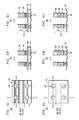
- FIG. 1 depicts a cross-sectional view of a MTJ device after a typical IBE process.
- FIG. 2A depicts a plan view of a starting MTJ device, in accordance with a first step an illustrative embodiment
- FIG. 2B depicts a cross-sectional view of the MTJ device, taken along the line A-A of FIG. 2A , in accordance with an illustrative embodiment
- FIG. 2C depicts a cross-sectional view of the MTJ device, taken along the line B-B of FIG. 2A , in accordance with an illustrative embodiment
- FIG. 3A depicts a plan view of a MTJ device, in accordance with another step in an illustrative embodiment
- FIG. 3B depicts a cross-sectional view of the MTJ device, taken along the line A-A of FIG. 3A , in accordance with an illustrative embodiment
- FIG. 3C depicts a cross-sectional view of the MTJ device, taken along the line B-B of FIG. 3A , in accordance with an illustrative embodiment
- FIG. 4A depicts a plan view of a MTJ device, in accordance with another step in an illustrative embodiment
- FIG. 4B depicts a cross-sectional view of the MTJ device, taken along the line A-A of FIG. 4A , in accordance with an illustrative embodiment
- FIG. 4C depicts a cross-sectional view of the MTJ device, taken along the line B-B of FIG. 4A , in accordance with an illustrative embodiment
- FIG. 5A depicts a plan view of a MTJ device, in accordance with another step in an illustrative embodiment
- FIG. 5B depicts a cross-sectional view of the MTJ device, taken along the line A-A of FIG. 5A , in accordance with an illustrative embodiment
- FIG. 5C depicts a cross-sectional view of the MTJ device, taken along the line B-B of FIG. 5A , in accordance with an illustrative embodiment
- FIG. 6A depicts a plan view of a MTJ device, in accordance with another step in an illustrative embodiment
- FIG. 6B depicts a cross-sectional view of the MTJ device, taken along the line A-A of FIG. 6A , in accordance with an illustrative embodiment
- FIG. 6C depicts a cross-sectional view of the MTJ device, taken along the line B-B of FIG. 6A , in accordance with an illustrative embodiment
- FIG. 7A depicts a plan view of a MTJ device, in accordance with another step an illustrative embodiment
- FIG. 7B depicts a cross-sectional view of the MTJ device, taken along the line A-A of FIG. 7A , in accordance with an illustrative embodiment
- FIG. 7C depicts a cross-sectional view of the MTJ device, taken along the line B-B of FIG. 7A , in accordance with an illustrative embodiment
- FIG. 7D depicts a cross-sectional view of the MTJ device, taken along the line C-C of FIG. 7A , in accordance with an illustrative embodiment.
- a MJT device according to the present invention is rotated during the IBE process. Compared with a pure IBE or RIE process, use of the rotation described herein will ensure that the sidewall damage is removed during the IBE process.
- the present invention provides a method to obtain improved sidewall profiles.
- the sidewall profiles refer to the sides of the pillars of the patterned junctions or sides of MTJ pillars as shown in FIGS. 2A-7D .
- MTJ device 12 includes the recess 15 of the bottom electrode 10 that cannot be avoided during a typical IBE or RIE process.
- FIG. 2A is a plan view of a starting MTJ device 100 for a first step of a method of the present invention
- FIG. 2B is a cross-sectional view of the starting MTJ device 100 , taken along the line A-A of FIG. 2A
- FIG. 2C is a cross-sectional view of the starting MTJ device 100 , taken along the line B-B of FIG. 2A .
- the MTJ device 100 comprises a substrate 101 with a plurality of bottom electrodes or bit line contacts 102 , a MTJ layer 104 disposed on substrate 101 including plurality of bottom electrodes/bit line contacts 102 , and a plurality of pillars comprising metal layer 106 and hardmask layer 108 disposed on MTJ layer 104 and positioned above the plurality of bottom electrodes/bit line contacts 102 .
- the bottom electrodes comprise a typical back-end-of line metal and/or bit line contact metal depending on the circuit design layout.
- the bottom electrodes 102 include, for example, conducting but non-magnetic metal.
- the MTJ layer 104 disposed on substrate 101 can be comprised of various layers in a stacked configuration.
- MTJ layer 104 can include a plurality of magnetic thin films with a tunnel barrier.
- a MTJ with an oxide tunnel barrier is used.
- the plurality of magnetic thin films include, for example, cobalt, iron, nickel, cobalt alloy, iron alloy, nickel alloy, nitrides and oxides, e.g., Fe, CoFe, CoFeB, etc.
- a tunnel barrier includes, for example, tantalum, titanium, ruthenium, magnesium, aluminum, copper, tantalum alloy, titanium alloy, ruthenium alloy, magnesium alloy, aluminum alloy, copper alloy, and nitrides and oxides, e.g., MgO.
- MTJ layer 104 can include a bottom electrode layer, a seed layer, a bottom fixed magnetic layer, a thin dielectric tunnel barrier and a free top magnetic layer in a stacked configuration.
- Hard mask metal pillars are formed on MTJ layer 104 by methods known in the art. For example, a metal layer 106 can first be disposed on MTJ layer 104 followed by a hard mask 108 being disposed on the metal layer 106 . Next, the hard mask can be patterned using a mask template to form the pillars of metal layers 106 and hard mask 108 . The hard mask metal pillars form a template to etch the MTJ layer 104 into MTJ pillars as described below.
- Metal layers 106 can be formed of a non-magnetic metallic material such as, for example, tantalum nitride and titanium nitride.
- Hard mask 108 can be formed of any known hard mask material such as, for example, silicon nitride and silicon dioxide.
- the hard mask metal pillars are disposed on substrate 101 such that they are position above the plurality of bottom electrodes/bit line contacts 102 . Now, the IBE process according to an embodiment is performed.
- an IBE process is performed where the MTJ device 100 is maintained at its starting position, i.e., at 0 degrees of MTJ device 100 .
- the ion beam is entering from a 0 degree orientation of the pillar array from top down view.
- the starting point of 0 degree is determined after deciding the 90 degree orientation.
- MTJ pillars in a unit cell are residing at four corners of the substrate in a rectangle or square shape.
- MTJ arrays are a repeating pattern of the unit cell.
- An MTJ unit cell can be in, for example, a diamond shape.
- the starting point of the IBE direction is any orientation to maximize the ion beam etching and minimize the shadowing of etching.
- Ion beam etching is typically performed at a tilt angle with respect to the substrate's surface.
- the IBE process is performed where the ion beam is directed at a tilt angle 110 relative to substrate's surface.
- an IBE angle with respect to the substrate's surface is from about 10 to about 80 degrees or from about 30 to about 50 degrees depending on, for example, the size, height, and spacing between pillars.
- an acceptable etch rate for manufacturing ranges from about 0.1 to about 10 A/s.
- the MTJ stack height will determine the total etching time.
- FIG. 3A is a plan view of a MTJ device 100 for another step of a method of the present invention
- FIG. 3B is a cross-sectional view of the starting MTJ device 100 , taken along the line A-A of FIG. 3A
- FIG. 3C is a cross-sectional view of the starting MTJ device 100 , taken along the line B-B of FIG. 3A
- the next step in the method according to the present invention involves rotating MTJ device 100 by 90 degrees in a clockwise or a counter clockwise direction about an axis perpendicular to a top surface of MTJ device 100 from the starting position.
- MTJ device 100 is shown being rotated by 90 degrees in a clockwise direction about an axis perpendicular to a top surface of MTJ device 100 from the starting position.
- MTJ device 100 is rotated by 90 degrees in a clockwise direction about an axis perpendicular to a top surface of MTJ device 100 from the starting position.
- the IBE process in this step is performed where the ion beam is directed at the tilted angle 120 relative to substrate's surface of MTJ device 100 .
- This angle dependence of the IBE results in further removal of the horizontal surfaces of the MTJ layer 104 from the MTJ device 100 as compared to the vertical sidewalls thereby lengthening the vertical sidewalls in MTJ layer 104 which are coextensive with sidewalls for metal layer 106 and hard mask 108 , as shown in FIGS.
- an IBE angle with respect to the substrate's surface is from about 10 to about 80 degrees or from about 30 to about 50 degrees depending on, for example, the size, height, and spacing between pillars.
- an acceptable etch rate for manufacturing ranges from about 0.1 to about 10 A/s. As one skilled in the art will understand, the MTJ stack height will determine the total etching time.
- MTJ device 100 will be further rotated an additional 90 degrees in the clockwise or counter clockwise direction about an axis perpendicular to the top surface of MTJ device 100 as determined from the previous step and then subjected to the IBE process until the horizontal surfaces of the MTJ layer 104 are substantially removed from the MTJ device 100 thereby providing a plurality of pillars in square shape of MTJ layers 104 and metal layers 106 having a vertical profile of sidewalls 100 (see FIG. 6A-6C ) with little to no shadowing.
- FIG. 4A is a plan view of a MTJ device 100 for another step of a method of the present invention
- FIG. 4B is a cross-sectional view of the starting MTJ device 100 , taken along the line A-A of FIG. 4A
- FIG. 4C is a cross-sectional view of the starting MTJ device 100 , taken along the line B-B of FIG. 4A .
- MTJ device 100 is rotated by another 90 degrees in a clockwise direction about an axis perpendicular to a top surface of MTJ device 100 from the previous step, i.e., MTJ device 100 is rotated by 180 degrees in a clockwise direction about an axis perpendicular to a top surface of MTJ device 100 from the previous position.
- the IBE process in this step is performed where the ion beam is directed at the tilted angle 130 relative to substrate's surface of MTJ device 100 .
- an IBE angle with respect to the substrate's surface is from about 10 to about 80 degrees or from about 30 to about 50 degrees depending on, for example, the size, height, and spacing between pillars.
- an acceptable etch rate for manufacturing ranges from about 0.1 to about 10 A/s. As one skilled in the art will understand, the MTJ stack height will determine the total etching time.
- FIG. 5A is a plan view of a MTJ device 100 for another step of a method of the present invention
- FIG. 5B is a cross-sectional view of the starting MTJ device 100 , taken along the line A-A of FIG. 5A
- FIG. 5C is a cross-sectional view of the starting MTJ device 100 , taken along the line B-B of FIG. 5A .
- MTJ device 100 is rotated by another 90 degrees in a clockwise direction about an axis perpendicular to a top surface of MTJ device 100 from the previous step, i.e., MTJ device 100 is rotated by 270 degrees in a clockwise direction about an axis perpendicular to a top surface of MTJ device 100 from the previous position.
- the IBE process in this step is performed where the ion beam is directed at the tilted angle 140 relative to substrate's surface of MTJ device 100 .
- an IBE angle with respect to the substrate's surface is from about 10 to about 80 degrees or from about 30 to about 50 degrees depending on, for example, the size, height, and spacing between pillars.
- an acceptable etch rate for manufacturing ranges from about 0.1 to about 10 A/s. As one skilled in the art will understand, the MTJ stack height will determine the total etching time.
- FIG. 6A is a plan view of a MTJ device 100 for another step of a method of the present invention
- FIG. 6B is a cross-sectional view of the starting MTJ device 100 , taken along the line A-A of FIG. 6A
- FIG. 6C is a cross-sectional view of the starting MTJ device 100 , taken along the line B-B of FIG. 6A .
- MTJ device 100 is rotated by another 90 degrees in a clockwise direction about an axis perpendicular to a top surface of MTJ device 100 from the previous step, i.e., MTJ device 100 is rotated by 360 degrees in a clockwise direction about an axis perpendicular to a top surface of MTJ device 100 from the previous position.
- the IBE process in this step is performed where the ion beam is directed at the tilted angle 150 relative to substrate's surface of MTJ device 100 .
- an IBE angle with respect to the substrate's surface is from about 10 to about 80 degrees or from about 30 to about 50 degrees depending on, for example, the size, height, and spacing between pillars.
- an acceptable etch rate for manufacturing ranges from about 0.1 to about 10 A/s. As one skilled in the art will understand, the MTJ stack height will determine the total etching time.
- FIG. 7A is a plan view of a MTJ device 100 for another step of a method of the present invention
- FIG. 7B is a cross-sectional view of the starting MTJ device 100 , taken along the line A-A of FIG. 7A
- FIG. 7C is a cross-sectional view of the starting MTJ device 100 , taken along the line B-B of FIG. 7A
- FIG. 7D is a cross-sectional view of the starting MTJ device 100 , taken along the line C-C of FIG. 7A .
- FIG. 7A is a plan view of a MTJ device 100 for another step of a method of the present invention
- FIG. 7B is a cross-sectional view of the starting MTJ device 100 , taken along the line A-A of FIG. 7A
- FIG. 7C is a cross-sectional view of the starting MTJ device 100 , taken along the line B-B of FIG. 7A
- FIG. 7D is a cross-sectional view
- the pillars of MTJ layer 104 , metal layer 106 and hard mask 108 are formed from a circular shape into a square shape as compared to the starting pillars of metal layer 106 and hard mask 108 which are in a circular shape (see FIGS. 2A-2C ).
- FIG. 7C illustrates that a recess is formed in the diagonal direction of substrate 102 after completion of the process due to redundant etching in these areas. If desired, one or more additional touch-up IBE with a quick rotational IBE mode can be carried out to smooth these shapes.
- integrated circuit dies can be fabricated with various devices such as transistors, diodes, capacitors, inductors, etc.
- An integrated circuit in accordance with embodiments can be employed in applications, hardware, and/or electronic systems. Suitable hardware and systems for implementing embodiments of the invention may include, but are not limited to, personal computers, communication networks, electronic commerce systems, portable communications devices (e.g., cell phones), solid-state media storage devices, functional circuitry, etc. Systems and hardware incorporating such integrated circuits are considered part of the embodiments described herein.
- various layers, regions, and/or structures described above may be implemented in integrated circuits (chips).
- the resulting integrated circuit chips can be distributed by the fabricator in raw wafer form (that is, as a single wafer that has multiple unpackaged chips), as a bare die, or in a packaged form.
- the chip is mounted in a single chip package (such as a plastic carrier, with leads that are affixed to a motherboard or other higher level carrier) or in a multichip package (such as a ceramic carrier that has either or both surface interconnections or buried interconnections).
- the chip is then integrated with other chips, discrete circuit elements, and/or other signal processing devices as part of either (a) an intermediate product, such as a motherboard, or (b) an end product.
- the end product can be any product that includes integrated circuit chips, ranging from toys and other low-end applications to advanced computer products having a display, a keyboard or other input device, and a central processor.
Landscapes
- Engineering & Computer Science (AREA)
- Power Engineering (AREA)
- Manufacturing & Machinery (AREA)
- Chemical & Material Sciences (AREA)
- Crystallography & Structural Chemistry (AREA)
- Computer Hardware Design (AREA)
- Nanotechnology (AREA)
- Physics & Mathematics (AREA)
- Spectroscopy & Molecular Physics (AREA)
- Mram Or Spin Memory Techniques (AREA)
- Hall/Mr Elements (AREA)
Abstract
Description
Claims (20)
Priority Applications (1)
| Application Number | Priority Date | Filing Date | Title |
|---|---|---|---|
| US15/899,933 US10693059B2 (en) | 2018-02-20 | 2018-02-20 | MTJ stack etch using IBE to achieve vertical profile |
Applications Claiming Priority (1)
| Application Number | Priority Date | Filing Date | Title |
|---|---|---|---|
| US15/899,933 US10693059B2 (en) | 2018-02-20 | 2018-02-20 | MTJ stack etch using IBE to achieve vertical profile |
Publications (2)
| Publication Number | Publication Date |
|---|---|
| US20190259939A1 US20190259939A1 (en) | 2019-08-22 |
| US10693059B2 true US10693059B2 (en) | 2020-06-23 |
Family
ID=67618162
Family Applications (1)
| Application Number | Title | Priority Date | Filing Date |
|---|---|---|---|
| US15/899,933 Active US10693059B2 (en) | 2018-02-20 | 2018-02-20 | MTJ stack etch using IBE to achieve vertical profile |
Country Status (1)
| Country | Link |
|---|---|
| US (1) | US10693059B2 (en) |
Families Citing this family (1)
| Publication number | Priority date | Publication date | Assignee | Title |
|---|---|---|---|---|
| CN116598194B (en) * | 2023-07-17 | 2023-09-29 | 致真存储(北京)科技有限公司 | Hard mask manufacturing method and memory |
Citations (14)
| Publication number | Priority date | Publication date | Assignee | Title |
|---|---|---|---|---|
| US20060014346A1 (en) * | 2004-07-16 | 2006-01-19 | Headway Technologies, Inc. | Magnetic random access memory array with thin conduction electrical read and write lines |
| US7352021B2 (en) | 2003-07-10 | 2008-04-01 | Samsung Electronics Co., Ltd. | Magnetic random access memory devices having titanium-rich lower electrodes with oxide layer and oriented tunneling barrier |
| US7531367B2 (en) | 2006-01-18 | 2009-05-12 | International Business Machines Corporation | Utilizing sidewall spacer features to form magnetic tunnel junctions in an integrated circuit |
| KR100975803B1 (en) | 2004-07-16 | 2010-08-16 | 헤드웨이 테크놀로지스 인코포레이티드 | An MTJ MRAM cell, an array of MTJ MRAM cells, and a method of forming an MTJ MRAM cell |
| US8334213B2 (en) | 2009-06-05 | 2012-12-18 | Magic Technologies, Inc. | Bottom electrode etching process in MRAM cell |
| US20130316536A1 (en) | 2012-05-22 | 2013-11-28 | Kabushiki Kaisha Toshiba | Semiconductor manufacturing device and semiconductor device manufacturing method |
| US20140084402A1 (en) * | 2012-09-25 | 2014-03-27 | Kabushiki Kaisha Toshiba | Magnetic memory |
| US20140248718A1 (en) | 2013-03-04 | 2014-09-04 | Jisoo Kim | Patterning of magnetic tunnel junction (mtj) film stacks |
| US8969982B2 (en) | 2006-09-28 | 2015-03-03 | Headway Technologies, Inc. | Bottom electrode for MRAM device |
| US20150255507A1 (en) | 2014-03-07 | 2015-09-10 | Applied Materials, Inc. | Method of forming magnetic tunneling junctions |
| US20150263273A1 (en) * | 2014-03-12 | 2015-09-17 | Masatoshi Yoshikawa | Magnetic memory having magnetoresistive element and method of manufacturing magnetoresistive element |
| US9287494B1 (en) | 2013-06-28 | 2016-03-15 | Western Digital (Fremont), Llc | Magnetic tunnel junction (MTJ) with a magnesium oxide tunnel barrier |
| US20160111472A1 (en) | 2014-02-28 | 2016-04-21 | SK Hynix Inc. | Electronic device and method for fabricating the same |
| US9666792B2 (en) | 2015-08-12 | 2017-05-30 | Qualcomm Incorporated | Shadow-effect compensated fabrication of magnetic tunnel junction (MTJ) elements |
-
2018
- 2018-02-20 US US15/899,933 patent/US10693059B2/en active Active
Patent Citations (14)
| Publication number | Priority date | Publication date | Assignee | Title |
|---|---|---|---|---|
| US7352021B2 (en) | 2003-07-10 | 2008-04-01 | Samsung Electronics Co., Ltd. | Magnetic random access memory devices having titanium-rich lower electrodes with oxide layer and oriented tunneling barrier |
| KR100975803B1 (en) | 2004-07-16 | 2010-08-16 | 헤드웨이 테크놀로지스 인코포레이티드 | An MTJ MRAM cell, an array of MTJ MRAM cells, and a method of forming an MTJ MRAM cell |
| US20060014346A1 (en) * | 2004-07-16 | 2006-01-19 | Headway Technologies, Inc. | Magnetic random access memory array with thin conduction electrical read and write lines |
| US7531367B2 (en) | 2006-01-18 | 2009-05-12 | International Business Machines Corporation | Utilizing sidewall spacer features to form magnetic tunnel junctions in an integrated circuit |
| US8969982B2 (en) | 2006-09-28 | 2015-03-03 | Headway Technologies, Inc. | Bottom electrode for MRAM device |
| US8334213B2 (en) | 2009-06-05 | 2012-12-18 | Magic Technologies, Inc. | Bottom electrode etching process in MRAM cell |
| US20130316536A1 (en) | 2012-05-22 | 2013-11-28 | Kabushiki Kaisha Toshiba | Semiconductor manufacturing device and semiconductor device manufacturing method |
| US20140084402A1 (en) * | 2012-09-25 | 2014-03-27 | Kabushiki Kaisha Toshiba | Magnetic memory |
| US20140248718A1 (en) | 2013-03-04 | 2014-09-04 | Jisoo Kim | Patterning of magnetic tunnel junction (mtj) film stacks |
| US9287494B1 (en) | 2013-06-28 | 2016-03-15 | Western Digital (Fremont), Llc | Magnetic tunnel junction (MTJ) with a magnesium oxide tunnel barrier |
| US20160111472A1 (en) | 2014-02-28 | 2016-04-21 | SK Hynix Inc. | Electronic device and method for fabricating the same |
| US20150255507A1 (en) | 2014-03-07 | 2015-09-10 | Applied Materials, Inc. | Method of forming magnetic tunneling junctions |
| US20150263273A1 (en) * | 2014-03-12 | 2015-09-17 | Masatoshi Yoshikawa | Magnetic memory having magnetoresistive element and method of manufacturing magnetoresistive element |
| US9666792B2 (en) | 2015-08-12 | 2017-05-30 | Qualcomm Incorporated | Shadow-effect compensated fabrication of magnetic tunnel junction (MTJ) elements |
Also Published As
| Publication number | Publication date |
|---|---|
| US20190259939A1 (en) | 2019-08-22 |
Similar Documents
| Publication | Publication Date | Title |
|---|---|---|
| US9577183B2 (en) | Methods of manufacturing a magnetoresistive random access memory device | |
| CN109979961B (en) | Magnetoresistive random access memory structure and manufacturing method thereof | |
| TWI593147B (en) | Magnetic tunnel junction and 3-d magnetic tunnel junction array | |
| US7001783B2 (en) | Mask schemes for patterning magnetic tunnel junctions | |
| US8278122B2 (en) | Method for forming MTJ cells | |
| US7476919B2 (en) | MRAM cell structure and method of fabrication | |
| TWI520392B (en) | Magnetoresistive random access memory (mram) device and method for fabricating the same | |
| US20080211055A1 (en) | Utilizing Sidewall Spacer Features to Form Magnetic Tunnel Junctions in an Integrated Circuit | |
| US11800812B2 (en) | Integrated circuit | |
| US9412935B1 (en) | Method for fabricating magnetic tunnel junction and 3-D magnetic tunnel junction array | |
| US11856864B2 (en) | Sub 60nm etchless MRAM devices by ion beam etching fabricated T-shaped bottom electrode | |
| KR20120135581A (en) | Method for forming a magnatic pattern and method for manufacturing a mram using the same | |
| US20210376232A1 (en) | Multilayer magnetic tunnel junction etching method and mram device | |
| US11152561B2 (en) | Magnetic memory device | |
| US20230360686A1 (en) | Magnetoresistive memory device and manufacturing method thereof | |
| TW202224179A (en) | Integrated circuit and method for forming memory cell | |
| US11895928B2 (en) | Integration scheme for three terminal spin-orbit-torque (SOT) switching devices | |
| US10693059B2 (en) | MTJ stack etch using IBE to achieve vertical profile | |
| US8477531B2 (en) | Spin torque transfer magnetoresistive random access memory in disk base with reduced threshold current | |
| US20230039834A1 (en) | Dual spacer for double magnetic tunnel junction devices | |
| TW201523944A (en) | Magnetoresistive element and method of manufacturing the same | |
| US20230104744A1 (en) | Magnetic memory device and method for manufacturing the same | |
| US20240130244A1 (en) | Chamfered mram device structure | |
| US11942128B2 (en) | Magnetic memory device | |
| US20240130243A1 (en) | Magnetic tunnel junction device |
Legal Events
| Date | Code | Title | Description |
|---|---|---|---|
| AS | Assignment |
Owner name: INTERNATIONAL BUSINESS MACHINES CORPORATION, NEW Y Free format text: ASSIGNMENT OF ASSIGNORS INTEREST;ASSIGNORS:SEO, SOON-CHEON;CHUNG, KISUP;OK, INJO;AND OTHERS;SIGNING DATES FROM 20180208 TO 20180214;REEL/FRAME:044977/0754 Owner name: INTERNATIONAL BUSINESS MACHINES CORPORATION, NEW YORK Free format text: ASSIGNMENT OF ASSIGNORS INTEREST;ASSIGNORS:SEO, SOON-CHEON;CHUNG, KISUP;OK, INJO;AND OTHERS;SIGNING DATES FROM 20180208 TO 20180214;REEL/FRAME:044977/0754 |
|
| FEPP | Fee payment procedure |
Free format text: ENTITY STATUS SET TO UNDISCOUNTED (ORIGINAL EVENT CODE: BIG.); ENTITY STATUS OF PATENT OWNER: LARGE ENTITY |
|
| STPP | Information on status: patent application and granting procedure in general |
Free format text: NOTICE OF ALLOWANCE MAILED -- APPLICATION RECEIVED IN OFFICE OF PUBLICATIONS |
|
| STPP | Information on status: patent application and granting procedure in general |
Free format text: AWAITING TC RESP., ISSUE FEE NOT PAID |
|
| STPP | Information on status: patent application and granting procedure in general |
Free format text: DOCKETED NEW CASE - READY FOR EXAMINATION |
|
| STPP | Information on status: patent application and granting procedure in general |
Free format text: NOTICE OF ALLOWANCE MAILED -- APPLICATION RECEIVED IN OFFICE OF PUBLICATIONS |
|
| STPP | Information on status: patent application and granting procedure in general |
Free format text: PUBLICATIONS -- ISSUE FEE PAYMENT RECEIVED |
|
| STCF | Information on status: patent grant |
Free format text: PATENTED CASE |
|
| MAFP | Maintenance fee payment |
Free format text: PAYMENT OF MAINTENANCE FEE, 4TH YEAR, LARGE ENTITY (ORIGINAL EVENT CODE: M1551); ENTITY STATUS OF PATENT OWNER: LARGE ENTITY Year of fee payment: 4 |