US10692832B2 - Manufacturing method of semiconductor structure - Google Patents
Manufacturing method of semiconductor structure Download PDFInfo
- Publication number
- US10692832B2 US10692832B2 US16/017,655 US201816017655A US10692832B2 US 10692832 B2 US10692832 B2 US 10692832B2 US 201816017655 A US201816017655 A US 201816017655A US 10692832 B2 US10692832 B2 US 10692832B2
- Authority
- US
- United States
- Prior art keywords
- bump
- pad
- pads
- solder ball
- solder
- Prior art date
- Legal status (The legal status is an assumption and is not a legal conclusion. Google has not performed a legal analysis and makes no representation as to the accuracy of the status listed.)
- Active
Links
- 239000004065 semiconductor Substances 0.000 title claims abstract description 78
- 238000004519 manufacturing process Methods 0.000 title description 9
- 229910000679 solder Inorganic materials 0.000 claims abstract description 85
- 238000000034 method Methods 0.000 claims abstract description 41
- 239000000758 substrate Substances 0.000 claims abstract description 37
- 239000000463 material Substances 0.000 claims description 24
- 238000009736 wetting Methods 0.000 description 9
- 239000000853 adhesive Substances 0.000 description 3
- 230000001070 adhesive effect Effects 0.000 description 3
- 238000009826 distribution Methods 0.000 description 3
- 238000001125 extrusion Methods 0.000 description 3
- 239000000203 mixture Substances 0.000 description 3
- RYGMFSIKBFXOCR-UHFFFAOYSA-N Copper Chemical compound [Cu] RYGMFSIKBFXOCR-UHFFFAOYSA-N 0.000 description 2
- 239000004020 conductor Substances 0.000 description 2
- 229910052802 copper Inorganic materials 0.000 description 2
- 239000010949 copper Substances 0.000 description 2
- 238000004806 packaging method and process Methods 0.000 description 2
- -1 polyethylene Polymers 0.000 description 2
- 229920000642 polymer Polymers 0.000 description 2
- 229920001296 polysiloxane Polymers 0.000 description 2
- 229920002635 polyurethane Polymers 0.000 description 2
- 239000004814 polyurethane Substances 0.000 description 2
- 229920000915 polyvinyl chloride Polymers 0.000 description 2
- 239000004800 polyvinyl chloride Substances 0.000 description 2
- 238000005476 soldering Methods 0.000 description 2
- KXGFMDJXCMQABM-UHFFFAOYSA-N 2-methoxy-6-methylphenol Chemical compound [CH]OC1=CC=CC([CH])=C1O KXGFMDJXCMQABM-UHFFFAOYSA-N 0.000 description 1
- 229920001342 Bakelite® Polymers 0.000 description 1
- 239000004593 Epoxy Substances 0.000 description 1
- 239000004677 Nylon Substances 0.000 description 1
- 239000004698 Polyethylene Substances 0.000 description 1
- 239000004743 Polypropylene Substances 0.000 description 1
- 239000004793 Polystyrene Substances 0.000 description 1
- BQCADISMDOOEFD-UHFFFAOYSA-N Silver Chemical compound [Ag] BQCADISMDOOEFD-UHFFFAOYSA-N 0.000 description 1
- NIXOWILDQLNWCW-UHFFFAOYSA-N acrylic acid group Chemical group C(C=C)(=O)O NIXOWILDQLNWCW-UHFFFAOYSA-N 0.000 description 1
- 229910045601 alloy Inorganic materials 0.000 description 1
- 239000000956 alloy Substances 0.000 description 1
- 229910052782 aluminium Inorganic materials 0.000 description 1
- XAGFODPZIPBFFR-UHFFFAOYSA-N aluminium Chemical compound [Al] XAGFODPZIPBFFR-UHFFFAOYSA-N 0.000 description 1
- 230000000712 assembly Effects 0.000 description 1
- 238000000429 assembly Methods 0.000 description 1
- 239000004637 bakelite Substances 0.000 description 1
- 239000003990 capacitor Substances 0.000 description 1
- 239000011248 coating agent Substances 0.000 description 1
- 238000000576 coating method Methods 0.000 description 1
- 150000001875 compounds Chemical class 0.000 description 1
- 238000005336 cracking Methods 0.000 description 1
- 238000010586 diagram Methods 0.000 description 1
- 238000001035 drying Methods 0.000 description 1
- 238000005530 etching Methods 0.000 description 1
- 230000004907 flux Effects 0.000 description 1
- 239000003292 glue Substances 0.000 description 1
- PCHJSUWPFVWCPO-UHFFFAOYSA-N gold Chemical compound [Au] PCHJSUWPFVWCPO-UHFFFAOYSA-N 0.000 description 1
- 229910052737 gold Inorganic materials 0.000 description 1
- 239000010931 gold Substances 0.000 description 1
- 229920001778 nylon Polymers 0.000 description 1
- 238000012858 packaging process Methods 0.000 description 1
- 229920001568 phenolic resin Polymers 0.000 description 1
- 238000000206 photolithography Methods 0.000 description 1
- 229920001084 poly(chloroprene) Polymers 0.000 description 1
- 229920002037 poly(vinyl butyral) polymer Polymers 0.000 description 1
- 229920002239 polyacrylonitrile Polymers 0.000 description 1
- 229910021420 polycrystalline silicon Inorganic materials 0.000 description 1
- 229920000573 polyethylene Polymers 0.000 description 1
- 229920001155 polypropylene Polymers 0.000 description 1
- 229920005591 polysilicon Polymers 0.000 description 1
- 229920002223 polystyrene Polymers 0.000 description 1
- 229910052710 silicon Inorganic materials 0.000 description 1
- 239000010703 silicon Substances 0.000 description 1
- 229910052709 silver Inorganic materials 0.000 description 1
- 239000004332 silver Substances 0.000 description 1
- 239000000126 substance Substances 0.000 description 1
- 229920003051 synthetic elastomer Polymers 0.000 description 1
- 239000005061 synthetic rubber Substances 0.000 description 1
- 125000000391 vinyl group Chemical group [H]C([*])=C([H])[H] 0.000 description 1
- 229920002554 vinyl polymer Polymers 0.000 description 1
- 230000000007 visual effect Effects 0.000 description 1
Images


Classifications
-
- H—ELECTRICITY
- H01—ELECTRIC ELEMENTS
- H01L—SEMICONDUCTOR DEVICES NOT COVERED BY CLASS H10
- H01L24/00—Arrangements for connecting or disconnecting semiconductor or solid-state bodies; Methods or apparatus related thereto
- H01L24/01—Means for bonding being attached to, or being formed on, the surface to be connected, e.g. chip-to-package, die-attach, "first-level" interconnects; Manufacturing methods related thereto
- H01L24/10—Bump connectors ; Manufacturing methods related thereto
- H01L24/15—Structure, shape, material or disposition of the bump connectors after the connecting process
- H01L24/17—Structure, shape, material or disposition of the bump connectors after the connecting process of a plurality of bump connectors
-
- H—ELECTRICITY
- H01—ELECTRIC ELEMENTS
- H01L—SEMICONDUCTOR DEVICES NOT COVERED BY CLASS H10
- H01L23/00—Details of semiconductor or other solid state devices
- H01L23/48—Arrangements for conducting electric current to or from the solid state body in operation, e.g. leads, terminal arrangements ; Selection of materials therefor
- H01L23/488—Arrangements for conducting electric current to or from the solid state body in operation, e.g. leads, terminal arrangements ; Selection of materials therefor consisting of soldered or bonded constructions
- H01L23/498—Leads, i.e. metallisations or lead-frames on insulating substrates, e.g. chip carriers
- H01L23/49838—Geometry or layout
-
- H—ELECTRICITY
- H01—ELECTRIC ELEMENTS
- H01L—SEMICONDUCTOR DEVICES NOT COVERED BY CLASS H10
- H01L23/00—Details of semiconductor or other solid state devices
- H01L23/48—Arrangements for conducting electric current to or from the solid state body in operation, e.g. leads, terminal arrangements ; Selection of materials therefor
- H01L23/488—Arrangements for conducting electric current to or from the solid state body in operation, e.g. leads, terminal arrangements ; Selection of materials therefor consisting of soldered or bonded constructions
- H01L23/498—Leads, i.e. metallisations or lead-frames on insulating substrates, e.g. chip carriers
- H01L23/49866—Leads, i.e. metallisations or lead-frames on insulating substrates, e.g. chip carriers characterised by the materials
- H01L23/49894—Materials of the insulating layers or coatings
-
- H—ELECTRICITY
- H01—ELECTRIC ELEMENTS
- H01L—SEMICONDUCTOR DEVICES NOT COVERED BY CLASS H10
- H01L24/00—Arrangements for connecting or disconnecting semiconductor or solid-state bodies; Methods or apparatus related thereto
- H01L24/01—Means for bonding being attached to, or being formed on, the surface to be connected, e.g. chip-to-package, die-attach, "first-level" interconnects; Manufacturing methods related thereto
- H01L24/02—Bonding areas ; Manufacturing methods related thereto
- H01L24/04—Structure, shape, material or disposition of the bonding areas prior to the connecting process
- H01L24/06—Structure, shape, material or disposition of the bonding areas prior to the connecting process of a plurality of bonding areas
-
- H—ELECTRICITY
- H01—ELECTRIC ELEMENTS
- H01L—SEMICONDUCTOR DEVICES NOT COVERED BY CLASS H10
- H01L24/00—Arrangements for connecting or disconnecting semiconductor or solid-state bodies; Methods or apparatus related thereto
- H01L24/80—Methods for connecting semiconductor or other solid state bodies using means for bonding being attached to, or being formed on, the surface to be connected
- H01L24/81—Methods for connecting semiconductor or other solid state bodies using means for bonding being attached to, or being formed on, the surface to be connected using a bump connector
-
- H—ELECTRICITY
- H01—ELECTRIC ELEMENTS
- H01L—SEMICONDUCTOR DEVICES NOT COVERED BY CLASS H10
- H01L2224/00—Indexing scheme for arrangements for connecting or disconnecting semiconductor or solid-state bodies and methods related thereto as covered by H01L24/00
- H01L2224/01—Means for bonding being attached to, or being formed on, the surface to be connected, e.g. chip-to-package, die-attach, "first-level" interconnects; Manufacturing methods related thereto
- H01L2224/02—Bonding areas; Manufacturing methods related thereto
- H01L2224/04—Structure, shape, material or disposition of the bonding areas prior to the connecting process
- H01L2224/0401—Bonding areas specifically adapted for bump connectors, e.g. under bump metallisation [UBM]
-
- H—ELECTRICITY
- H01—ELECTRIC ELEMENTS
- H01L—SEMICONDUCTOR DEVICES NOT COVERED BY CLASS H10
- H01L2224/00—Indexing scheme for arrangements for connecting or disconnecting semiconductor or solid-state bodies and methods related thereto as covered by H01L24/00
- H01L2224/01—Means for bonding being attached to, or being formed on, the surface to be connected, e.g. chip-to-package, die-attach, "first-level" interconnects; Manufacturing methods related thereto
- H01L2224/02—Bonding areas; Manufacturing methods related thereto
- H01L2224/04—Structure, shape, material or disposition of the bonding areas prior to the connecting process
- H01L2224/05—Structure, shape, material or disposition of the bonding areas prior to the connecting process of an individual bonding area
- H01L2224/0554—External layer
- H01L2224/0556—Disposition
- H01L2224/05568—Disposition the whole external layer protruding from the surface
-
- H—ELECTRICITY
- H01—ELECTRIC ELEMENTS
- H01L—SEMICONDUCTOR DEVICES NOT COVERED BY CLASS H10
- H01L2224/00—Indexing scheme for arrangements for connecting or disconnecting semiconductor or solid-state bodies and methods related thereto as covered by H01L24/00
- H01L2224/01—Means for bonding being attached to, or being formed on, the surface to be connected, e.g. chip-to-package, die-attach, "first-level" interconnects; Manufacturing methods related thereto
- H01L2224/02—Bonding areas; Manufacturing methods related thereto
- H01L2224/04—Structure, shape, material or disposition of the bonding areas prior to the connecting process
- H01L2224/05—Structure, shape, material or disposition of the bonding areas prior to the connecting process of an individual bonding area
- H01L2224/0554—External layer
- H01L2224/05599—Material
-
- H—ELECTRICITY
- H01—ELECTRIC ELEMENTS
- H01L—SEMICONDUCTOR DEVICES NOT COVERED BY CLASS H10
- H01L2224/00—Indexing scheme for arrangements for connecting or disconnecting semiconductor or solid-state bodies and methods related thereto as covered by H01L24/00
- H01L2224/01—Means for bonding being attached to, or being formed on, the surface to be connected, e.g. chip-to-package, die-attach, "first-level" interconnects; Manufacturing methods related thereto
- H01L2224/02—Bonding areas; Manufacturing methods related thereto
- H01L2224/04—Structure, shape, material or disposition of the bonding areas prior to the connecting process
- H01L2224/06—Structure, shape, material or disposition of the bonding areas prior to the connecting process of a plurality of bonding areas
- H01L2224/0651—Function
- H01L2224/06515—Bonding areas having different functions
- H01L2224/06517—Bonding areas having different functions including bonding areas providing primarily mechanical bonding
-
- H—ELECTRICITY
- H01—ELECTRIC ELEMENTS
- H01L—SEMICONDUCTOR DEVICES NOT COVERED BY CLASS H10
- H01L2224/00—Indexing scheme for arrangements for connecting or disconnecting semiconductor or solid-state bodies and methods related thereto as covered by H01L24/00
- H01L2224/01—Means for bonding being attached to, or being formed on, the surface to be connected, e.g. chip-to-package, die-attach, "first-level" interconnects; Manufacturing methods related thereto
- H01L2224/02—Bonding areas; Manufacturing methods related thereto
- H01L2224/07—Structure, shape, material or disposition of the bonding areas after the connecting process
- H01L2224/09—Structure, shape, material or disposition of the bonding areas after the connecting process of a plurality of bonding areas
- H01L2224/0951—Function
- H01L2224/09515—Bonding areas having different functions
- H01L2224/09517—Bonding areas having different functions including bonding areas providing primarily mechanical support
-
- H—ELECTRICITY
- H01—ELECTRIC ELEMENTS
- H01L—SEMICONDUCTOR DEVICES NOT COVERED BY CLASS H10
- H01L2224/00—Indexing scheme for arrangements for connecting or disconnecting semiconductor or solid-state bodies and methods related thereto as covered by H01L24/00
- H01L2224/01—Means for bonding being attached to, or being formed on, the surface to be connected, e.g. chip-to-package, die-attach, "first-level" interconnects; Manufacturing methods related thereto
- H01L2224/10—Bump connectors; Manufacturing methods related thereto
- H01L2224/1012—Auxiliary members for bump connectors, e.g. spacers
- H01L2224/10122—Auxiliary members for bump connectors, e.g. spacers being formed on the semiconductor or solid-state body to be connected
- H01L2224/10135—Alignment aids
-
- H—ELECTRICITY
- H01—ELECTRIC ELEMENTS
- H01L—SEMICONDUCTOR DEVICES NOT COVERED BY CLASS H10
- H01L2224/00—Indexing scheme for arrangements for connecting or disconnecting semiconductor or solid-state bodies and methods related thereto as covered by H01L24/00
- H01L2224/01—Means for bonding being attached to, or being formed on, the surface to be connected, e.g. chip-to-package, die-attach, "first-level" interconnects; Manufacturing methods related thereto
- H01L2224/10—Bump connectors; Manufacturing methods related thereto
- H01L2224/11—Manufacturing methods
- H01L2224/113—Manufacturing methods by local deposition of the material of the bump connector
- H01L2224/1133—Manufacturing methods by local deposition of the material of the bump connector in solid form
- H01L2224/1134—Stud bumping, i.e. using a wire-bonding apparatus
-
- H—ELECTRICITY
- H01—ELECTRIC ELEMENTS
- H01L—SEMICONDUCTOR DEVICES NOT COVERED BY CLASS H10
- H01L2224/00—Indexing scheme for arrangements for connecting or disconnecting semiconductor or solid-state bodies and methods related thereto as covered by H01L24/00
- H01L2224/01—Means for bonding being attached to, or being formed on, the surface to be connected, e.g. chip-to-package, die-attach, "first-level" interconnects; Manufacturing methods related thereto
- H01L2224/10—Bump connectors; Manufacturing methods related thereto
- H01L2224/12—Structure, shape, material or disposition of the bump connectors prior to the connecting process
- H01L2224/13—Structure, shape, material or disposition of the bump connectors prior to the connecting process of an individual bump connector
- H01L2224/13001—Core members of the bump connector
- H01L2224/1301—Shape
- H01L2224/13012—Shape in top view
- H01L2224/13014—Shape in top view being circular or elliptic
-
- H—ELECTRICITY
- H01—ELECTRIC ELEMENTS
- H01L—SEMICONDUCTOR DEVICES NOT COVERED BY CLASS H10
- H01L2224/00—Indexing scheme for arrangements for connecting or disconnecting semiconductor or solid-state bodies and methods related thereto as covered by H01L24/00
- H01L2224/01—Means for bonding being attached to, or being formed on, the surface to be connected, e.g. chip-to-package, die-attach, "first-level" interconnects; Manufacturing methods related thereto
- H01L2224/10—Bump connectors; Manufacturing methods related thereto
- H01L2224/12—Structure, shape, material or disposition of the bump connectors prior to the connecting process
- H01L2224/13—Structure, shape, material or disposition of the bump connectors prior to the connecting process of an individual bump connector
- H01L2224/13001—Core members of the bump connector
- H01L2224/13099—Material
- H01L2224/131—Material with a principal constituent of the material being a metal or a metalloid, e.g. boron [B], silicon [Si], germanium [Ge], arsenic [As], antimony [Sb], tellurium [Te] and polonium [Po], and alloys thereof
-
- H—ELECTRICITY
- H01—ELECTRIC ELEMENTS
- H01L—SEMICONDUCTOR DEVICES NOT COVERED BY CLASS H10
- H01L2224/00—Indexing scheme for arrangements for connecting or disconnecting semiconductor or solid-state bodies and methods related thereto as covered by H01L24/00
- H01L2224/01—Means for bonding being attached to, or being formed on, the surface to be connected, e.g. chip-to-package, die-attach, "first-level" interconnects; Manufacturing methods related thereto
- H01L2224/10—Bump connectors; Manufacturing methods related thereto
- H01L2224/15—Structure, shape, material or disposition of the bump connectors after the connecting process
- H01L2224/16—Structure, shape, material or disposition of the bump connectors after the connecting process of an individual bump connector
- H01L2224/161—Disposition
- H01L2224/16151—Disposition the bump connector connecting between a semiconductor or solid-state body and an item not being a semiconductor or solid-state body, e.g. chip-to-substrate, chip-to-passive
- H01L2224/16221—Disposition the bump connector connecting between a semiconductor or solid-state body and an item not being a semiconductor or solid-state body, e.g. chip-to-substrate, chip-to-passive the body and the item being stacked
- H01L2224/16225—Disposition the bump connector connecting between a semiconductor or solid-state body and an item not being a semiconductor or solid-state body, e.g. chip-to-substrate, chip-to-passive the body and the item being stacked the item being non-metallic, e.g. insulating substrate with or without metallisation
- H01L2224/16237—Disposition the bump connector connecting between a semiconductor or solid-state body and an item not being a semiconductor or solid-state body, e.g. chip-to-substrate, chip-to-passive the body and the item being stacked the item being non-metallic, e.g. insulating substrate with or without metallisation the bump connector connecting to a bonding area disposed in a recess of the surface of the item
-
- H—ELECTRICITY
- H01—ELECTRIC ELEMENTS
- H01L—SEMICONDUCTOR DEVICES NOT COVERED BY CLASS H10
- H01L2224/00—Indexing scheme for arrangements for connecting or disconnecting semiconductor or solid-state bodies and methods related thereto as covered by H01L24/00
- H01L2224/01—Means for bonding being attached to, or being formed on, the surface to be connected, e.g. chip-to-package, die-attach, "first-level" interconnects; Manufacturing methods related thereto
- H01L2224/10—Bump connectors; Manufacturing methods related thereto
- H01L2224/15—Structure, shape, material or disposition of the bump connectors after the connecting process
- H01L2224/17—Structure, shape, material or disposition of the bump connectors after the connecting process of a plurality of bump connectors
- H01L2224/1701—Structure
- H01L2224/1703—Bump connectors having different sizes, e.g. different diameters, heights or widths
-
- H—ELECTRICITY
- H01—ELECTRIC ELEMENTS
- H01L—SEMICONDUCTOR DEVICES NOT COVERED BY CLASS H10
- H01L2224/00—Indexing scheme for arrangements for connecting or disconnecting semiconductor or solid-state bodies and methods related thereto as covered by H01L24/00
- H01L2224/01—Means for bonding being attached to, or being formed on, the surface to be connected, e.g. chip-to-package, die-attach, "first-level" interconnects; Manufacturing methods related thereto
- H01L2224/10—Bump connectors; Manufacturing methods related thereto
- H01L2224/15—Structure, shape, material or disposition of the bump connectors after the connecting process
- H01L2224/17—Structure, shape, material or disposition of the bump connectors after the connecting process of a plurality of bump connectors
- H01L2224/1751—Function
- H01L2224/17515—Bump connectors having different functions
- H01L2224/17517—Bump connectors having different functions including bump connectors providing primarily mechanical support
-
- H—ELECTRICITY
- H01—ELECTRIC ELEMENTS
- H01L—SEMICONDUCTOR DEVICES NOT COVERED BY CLASS H10
- H01L2224/00—Indexing scheme for arrangements for connecting or disconnecting semiconductor or solid-state bodies and methods related thereto as covered by H01L24/00
- H01L2224/80—Methods for connecting semiconductor or other solid state bodies using means for bonding being attached to, or being formed on, the surface to be connected
- H01L2224/81—Methods for connecting semiconductor or other solid state bodies using means for bonding being attached to, or being formed on, the surface to be connected using a bump connector
- H01L2224/8112—Aligning
- H01L2224/81136—Aligning involving guiding structures, e.g. spacers or supporting members
- H01L2224/81138—Aligning involving guiding structures, e.g. spacers or supporting members the guiding structures being at least partially left in the finished device
- H01L2224/81139—Guiding structures on the body
-
- H—ELECTRICITY
- H01—ELECTRIC ELEMENTS
- H01L—SEMICONDUCTOR DEVICES NOT COVERED BY CLASS H10
- H01L2224/00—Indexing scheme for arrangements for connecting or disconnecting semiconductor or solid-state bodies and methods related thereto as covered by H01L24/00
- H01L2224/80—Methods for connecting semiconductor or other solid state bodies using means for bonding being attached to, or being formed on, the surface to be connected
- H01L2224/81—Methods for connecting semiconductor or other solid state bodies using means for bonding being attached to, or being formed on, the surface to be connected using a bump connector
- H01L2224/8119—Arrangement of the bump connectors prior to mounting
- H01L2224/81191—Arrangement of the bump connectors prior to mounting wherein the bump connectors are disposed only on the semiconductor or solid-state body
-
- H—ELECTRICITY
- H01—ELECTRIC ELEMENTS
- H01L—SEMICONDUCTOR DEVICES NOT COVERED BY CLASS H10
- H01L2224/00—Indexing scheme for arrangements for connecting or disconnecting semiconductor or solid-state bodies and methods related thereto as covered by H01L24/00
- H01L2224/80—Methods for connecting semiconductor or other solid state bodies using means for bonding being attached to, or being formed on, the surface to be connected
- H01L2224/81—Methods for connecting semiconductor or other solid state bodies using means for bonding being attached to, or being formed on, the surface to be connected using a bump connector
- H01L2224/818—Bonding techniques
- H01L2224/81801—Soldering or alloying
- H01L2224/81815—Reflow soldering
-
- H—ELECTRICITY
- H01—ELECTRIC ELEMENTS
- H01L—SEMICONDUCTOR DEVICES NOT COVERED BY CLASS H10
- H01L24/00—Arrangements for connecting or disconnecting semiconductor or solid-state bodies; Methods or apparatus related thereto
- H01L24/01—Means for bonding being attached to, or being formed on, the surface to be connected, e.g. chip-to-package, die-attach, "first-level" interconnects; Manufacturing methods related thereto
- H01L24/02—Bonding areas ; Manufacturing methods related thereto
- H01L24/04—Structure, shape, material or disposition of the bonding areas prior to the connecting process
- H01L24/05—Structure, shape, material or disposition of the bonding areas prior to the connecting process of an individual bonding area
-
- H—ELECTRICITY
- H01—ELECTRIC ELEMENTS
- H01L—SEMICONDUCTOR DEVICES NOT COVERED BY CLASS H10
- H01L24/00—Arrangements for connecting or disconnecting semiconductor or solid-state bodies; Methods or apparatus related thereto
- H01L24/01—Means for bonding being attached to, or being formed on, the surface to be connected, e.g. chip-to-package, die-attach, "first-level" interconnects; Manufacturing methods related thereto
- H01L24/10—Bump connectors ; Manufacturing methods related thereto
- H01L24/12—Structure, shape, material or disposition of the bump connectors prior to the connecting process
- H01L24/13—Structure, shape, material or disposition of the bump connectors prior to the connecting process of an individual bump connector
-
- H—ELECTRICITY
- H01—ELECTRIC ELEMENTS
- H01L—SEMICONDUCTOR DEVICES NOT COVERED BY CLASS H10
- H01L24/00—Arrangements for connecting or disconnecting semiconductor or solid-state bodies; Methods or apparatus related thereto
- H01L24/01—Means for bonding being attached to, or being formed on, the surface to be connected, e.g. chip-to-package, die-attach, "first-level" interconnects; Manufacturing methods related thereto
- H01L24/10—Bump connectors ; Manufacturing methods related thereto
- H01L24/12—Structure, shape, material or disposition of the bump connectors prior to the connecting process
- H01L24/14—Structure, shape, material or disposition of the bump connectors prior to the connecting process of a plurality of bump connectors
-
- H—ELECTRICITY
- H01—ELECTRIC ELEMENTS
- H01L—SEMICONDUCTOR DEVICES NOT COVERED BY CLASS H10
- H01L24/00—Arrangements for connecting or disconnecting semiconductor or solid-state bodies; Methods or apparatus related thereto
- H01L24/01—Means for bonding being attached to, or being formed on, the surface to be connected, e.g. chip-to-package, die-attach, "first-level" interconnects; Manufacturing methods related thereto
- H01L24/10—Bump connectors ; Manufacturing methods related thereto
- H01L24/15—Structure, shape, material or disposition of the bump connectors after the connecting process
- H01L24/16—Structure, shape, material or disposition of the bump connectors after the connecting process of an individual bump connector
-
- H—ELECTRICITY
- H01—ELECTRIC ELEMENTS
- H01L—SEMICONDUCTOR DEVICES NOT COVERED BY CLASS H10
- H01L2924/00—Indexing scheme for arrangements or methods for connecting or disconnecting semiconductor or solid-state bodies as covered by H01L24/00
- H01L2924/0001—Technical content checked by a classifier
- H01L2924/00014—Technical content checked by a classifier the subject-matter covered by the group, the symbol of which is combined with the symbol of this group, being disclosed without further technical details
-
- H—ELECTRICITY
- H01—ELECTRIC ELEMENTS
- H01L—SEMICONDUCTOR DEVICES NOT COVERED BY CLASS H10
- H01L2924/00—Indexing scheme for arrangements or methods for connecting or disconnecting semiconductor or solid-state bodies as covered by H01L24/00
- H01L2924/013—Alloys
- H01L2924/014—Solder alloys
Definitions
- the disclosure relates to a structure, and more particularly to a semiconductor structure and a manufacturing method of the semiconductor.
- Chip scale packages are widely adopted for semiconductor chip assemblies in the industry because the component has a smaller size.
- a popular methodology of manufacturing a CSP component is a technology called surface mounting technology (SMT).
- SMT surface mounting technology
- the surface mounting technology is a method in which the semiconductor chip is mounted or placed directly on the surface of a printed circuit board (PCB).
- PCB printed circuit board
- a semiconductor component made with SMT usually has either smaller bonding wires or no bonding wires at all.
- the semiconductor component made with SMT is smaller in size and lower in electrical resistance.
- a ball grid array (BGA) is a type of packaging used for integrating the semiconductor chip and the printed circuit board.
- BGA packaging a number of solder balls are first disposed on either the pads of the semiconductor chip or the pads of the printed circuit board, and then the semiconductor chip and the circuit board are bonded through the solder balls.
- the resistance and required package space are both reduced.
- the reliability of the solder balls affects the manufacturing yield of the surface mounting technology. As such, improvements in the integrity and method for a solder ball to form in a surface mounting component continue to be sought.
- FIG. 1 is a cross sectional view of a semiconductor structure having a bump contacting an electrically insulative top surface on a circuit board in accordance with some embodiments of the present disclosure.
- FIG. 1A is a cross sectional view of a semiconductor structure having a bump contacting an electrically insulative top surface on a circuit board in accordance with some embodiments of the present disclosure.
- FIG. 2 is a cross sectional view of a semiconductor structure having a bump contacting with an insulative pad on circuit board in accordance with some embodiments of the present disclosure.
- FIG. 2A is a cross sectional view of a semiconductor structure having a bump contacting with an insulative pad in a recessed portion of a circuit board in accordance with some embodiments of the present disclosure.
- FIG. 3 is a cross sectional view of a semiconductor structure having a bump contacting with an insulative pad on circuit board in accordance with some embodiments of the present disclosure.
- FIG. 4 is a flowchart of a method 400 for fabricating a semiconductor structure bump according to various aspects of the present disclosure.
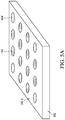
- FIGS. 5A to 5E are perspective views of a method of forming a semiconductor structure in accordance some embodiments of the present disclosure.
- FIG. 6 is the cross sectional view along line AA′ in FIG. 4E in accordance some embodiments of the present disclosure.
- FIG. 7 is the cross sectional view along line AA′ in FIG. 4E in accordance some embodiments of the present disclosure.
- FIGS. 8A-8C are top views of a pad array on a circuit board in accordance some embodiments of the present disclosure.
- bump is used as the connection member between the semiconductor device and the circuit board after the bonding processes.
- the different types of bumps are formed using a soldering material, for example, solder balls, or solder pastes.
- solder balls are bonded on the pads of a semiconductor device or a circuit board and form bumps to connect the semiconductor device with the circuit board. Stress distribution inside the bump is an issue. High stress in the corners of the bumps or on the contact surface between the bumps and the pad bonded thereon is causing the bumps to be vulnerable and may cause cracking and a bad electrical connection.
- a semiconductor structure or a SMT component having a number of bumps are bonded on a semiconductor device and configured to connect the semiconductor device with a circuit board.
- the bumps are elongated to have a smaller wetting angle with the pads of the semiconductor device or circuit.
- Each of the elongated bumps is designed to be capable of having a low stress distributed at the corners of the bumps.
- a method according to the present disclosure is designed to at least two different types of bumps in a surface mounting component or a chip scale package assembly.
- the first type is called active bump because the first type bump is conducting electrical current between the circuit board and the semiconductor device.
- the second type is non-active bump because the second type bump is not electrically connected with any circuitry neither in the circuit board nor the semiconductor device.
- the second type bump acts as a dummy bump.
- connection between non-active bump and the circuit board is in non-wetted manner.
- Active bump is elongated by a non-wetted non-active bump.
- Active bump is elongated to have a greater aspect ratio than the non-active bump.
- an active bump is taller than an adjacent non-active bump.
- FIG. 1 is a semiconductor structure 100 .
- the semiconductor structure 100 is a surface mounting component including a semiconductor device 105 and a circuit board 109 .
- the semiconductor device 105 has a semiconductor substrate 102 .
- a “semiconductor substrate” refers to a bulk semiconductor substrate on which various layers and device structure are formed.
- the bulk substrate includes silicon or a compound semiconductor, such as Ga As, InP, Si/Ge, or SiC.
- the layers include dielectric layers, doped layers, polysilicon layers or conductive layers.
- the device structures include transistors, resistors, and/or capacitors, which may be interconnected through an interconnect layer to additional integrated circuits.
- Pads 104 are disposed on a top surface 102 - 1 of the semiconductor substrate 102 .
- Pads 104 are electrically connected to an internal circuit in the semiconductor substrate 102 at one side and electrically connected to an active pad 108 of the circuit board 109 via a bump 120 .
- the pad 108 is disposed on a top surface 109 - 1 of the circuit board 109 .
- the top surface 109 - 1 is not a flat surface as in FIG. 1 .
- the top surface 109 includes some recessed portions 109 - 1 a to accommodate pads 108 .
- the circuit board 109 is designed to mechanically supports and electrically connects electronic components using conductive tracks, pads and other features etched from conductor sheets such as copper, laminated onto a non-conductive substrate.
- the circuit board 109 is a printed circuit board (PCB).
- a PCB populated with electronic components is called a printed circuit assembly (PCA), printed circuit board assembly or PCB assembly (PCBA).
- Pads 104 are active pads. Active pad herein means the pad is conductive and located on an electric current path connecting the circuit board 109 and the semiconductor substrate 102 . Like in FIG. 1 , an active pad 104 on the semiconductor substrate 102 is connecting with a bump 120 whereas an active pad 108 on the circuit board 109 is connected with. Thus, electrical current travels from either active pad 104 or 108 to the other side of the bump 120 .
- non-active pad means that the pad is not on an electric current path. In some embodiments, it is also called a dummy pad.
- a non-active pad 104 ′ is disposed on the top surface 102 - 1 but electrically insulated from the internal circuit of the semiconductor substrate 102 .
- the non-active pad 104 ′ is located correspondingly to a contact area 108 ′ on the top surface 109 - 1 of the circuit board 109 .
- the non-active pad 104 ′ is connected to a non-active bump 120 ′.
- the bump 120 ′ is in contact with an electrically insulative contact area 108 ′, therefore there is no electric current passing through the non-active pad 104 ′ while the semiconductor structure 100 is in operation.
- the contact area 108 ′ is a non-metallic surface.
- the non-active pad 104 ′ is a metallic layer such that the bump 120 ′ is in contact with the non-active pad 104 ′ in wetted manner.
- the surface of electrically insulative contact area 108 ′ is configured to be unwettable to the bump.
- the surface of electrically insulative contact area 108 ′ is a portion of an electrically insulative coating of circuit board 109 .
- the surface is coated with an insulative material that can not provide an adhesive force to overcome cohesive force of the bump when reflowed.
- the bump maintains a curvature surface at the point contacting with the electrically insulative contact area 108 ′. Therefore, bump such as 120 ′ is in contact with the contact area 108 ′ in non-wetted manner. There is no any metallic bonding between bump 120 ′ and the contact area 108 ′.
- the insulative material includes Acrylic, Epoxy, Polyurethane, Polyurethane, Silicones. The insulative material is ease of rework and operation in simple drying process, good moisture resistance, chemical resistant, and high dielectric constant.
- Pads 108 on the circuit board 109 are designed to include conductive material such as copper, aluminum, gold, silver, or alloys thereof, therefore the top surface of pads 108 provide an adhesive force adequate enough to overcome cohesive force of the bump when reflowed.
- the active bump 120 is in contact with the pad 108 in wetted manner.
- the active bump 120 has a greater contact area surface with pad 108 than the non-active bump 120 ′ with contact area 108 ′.
- the active bump 120 has a higher aspect ratio than the non-active bump 120 ′.
- the aspect ratio of each bump is defined as the ratio of the is height of the bump divided by the central width (full width at half height).
- solder material between pad 104 and pad 108 is elongated by solder material between pads 104 ′ and 108 ′ during reflow.
- the non-wetted curvature surface of the solder material on pad 108 ′ increase the gap between circuit board 109 and semiconductor substrate 102 .
- wetted soldering material is elongated to have a higher aspect ratio and a smaller wetting angle with pad 108 .
- the elongated solder material or bump are more resistant to any crack induced by stress. In FIG.
- bump 120 has a height H 1 and a central width W 1
- bump 120 ′ has a height H 2 and a central width W 2
- the bump 120 has an aspect ratio H 1 /W 1
- the bump 120 ′ has an aspect ratio H 2 /W 2 .
- H 1 /W 1 is greater than H 2 /W 2 .
- the active bump 120 has a wetting angle, ⁇ , which is the contact angle between the bump 120 and the active pad 108 of the circuit board 109 .
- the wetting angle ⁇ is substantially smaller than or equal to 90 degrees.
- the wetting angle ⁇ is substantially between about 80 degrees and 110 degrees.
- the wetting angle ⁇ is substantially between about 80 degrees and 130 degrees.
- the contact area 108 ′ in contact with the bump 120 ′ is an electrically insulative pad.
- a pad 107 is disposed on surface 109 - 1 .
- the surface 109 - 1 includes several substantially identical recessed portions 109 - 1 a and each recessed portion is configured to accommodate either an active pad 108 or a non-active pad 107 .
- the non-active pad 107 has a same thickness with the active pad 108 .
- top surface of the non-active pad 107 includes material not suitable for solder wetting.
- the non-active pad 107 includes polymeric material.
- the non-active pad 107 includes material such as synthetic rubber, phenol formaldehyde resin (or Bakelite), neoprene, nylon, polyvinyl chloride (PVC or vinyl), polystyrene, polyethylene, polypropylene, polyacrylonitrile, PVB, silicone.
- the pad 107 is located correspondingly to a non-active pad 104 ′ on the semiconductor substrate 102 . Because bump 120 ′ does can not be wetted on the top surface of the non-active pad during reflow, the bump 120 ′ maintains a curvature tip at one end. Bump wetted on pad 108 , such as 120 , is elongated to have a smaller width than the non-wetted bump 120 ′. Because both wetted bump 120 and non-wetted bump 120 ′ have a same height, the aspect ratio of wetted bump 120 is greater than the non-wetted bump 120 ′.
- the pad 107 on circuit board 109 is thicker than the pad 108 .
- the pad 107 has an extrusion d over the top surface 109 - 1 of circuit board 109 .
- the extrusion d is between predetermined ranges. In some embodiments, extrusion d is about one tenth of the thickness of the pad 107 . In some embodiments, extension d is between about one eighth and one tenth of the thickness of the pad 107 .
- the pad 107 is disposed on a portion of the top surface 109 - 1 that is at a higher level than the recessed portions 109 - 1 a . In other words, the pad 107 is disposed at a surface that is higher than the active pad 108 . Active bumps 120 are in contact with pad 108 in wetted manner, however, the non-active bump 120 ′ is contacting with pad 107 in non-wetted manner. Because the space between semiconductor substrate 102 and circuit board 109 is constrained at a fixed value S, the wetted bump 120 is elongated by non-wetted bumps 120 ′ to have a taller thickness than the non-wetted bump 120 ′.
- the wetted bump 120 also has a smaller wetting angle ⁇ 1 than the wetting angle ⁇ 2 of the non-wetted bump 120 ′.
- ⁇ 1 is about 10% to 15% smaller than ⁇ 2 .
- ⁇ 1 is about 10% to 30% smaller than ⁇ 2 .
- FIG. 4 is a flowchart of a method 400 for fabricating a semiconductor structure with non-wetted bump according to various aspects of the present disclosure.
- the method 400 includes operation 402 in which a semiconductor substrate is provided.
- the method 400 continues with operation 404 in which a pad is formed on a top surface of the semiconductor substrate.
- the method 400 continues with operation 406 in which a circuit board is provided. On the circuit, a contact area corresponding to the pad on the semiconductor substrate is provides.
- the method 400 continues with operation 408 in which a bump is formed between the semiconductor substrate and the circuit. The bump contacts the contact area provided on the circuit board in non-wetted manner.
- the various operations of FIG. 4 are discussed below in more detail in association with cross sectional or top views corresponding to the operations of the flow diagram.
- a semiconductor substrate 102 is provided.
- pads ( 104 , 104 ′) are formed on a top surface 102 - 1 of the semiconductor substrate 102 .
- the pads are arranged in an array.
- pads are designed for a SMT ball grid array (BGA) package.
- Some pads like 104 are active pads and some pads like 104 ′ are non-active or dummy pads.
- active pads 104 and non-active pads 104 ′ are drawn in different patterns. However, the pattern difference should not be deemed as a restriction to the present disclosure.
- a circuit board 109 is provided. On a top surface 109 - 1 of the circuit board 109 , there are several non-metallic contact areas 108 ′ are designed correspondingly to the non-active pad 104 ′ in FIG. 5A .
- the circuit board 109 also has some recessed portions 109 - 1 a , which are designed to accommodate active pads 108 .
- the distribution pattern of the active pads 108 on circuit board 109 is corresponding to the distribution pattern of the active pads 104 on the semiconductor substrate 102 in FIG. 5A .
- the contact area 108 ′ is a part of the top surface 109 - 1 hence that is not distinguishable from the top surface 109 - 1 . Dotted line is used to mean that the boundary between the contact area 108 ′ and the top surface 109 - 1 may be invisible for some embodiments.
- solder balls 122 are placed on pads 104 and 104 ′ as in FIG. 5C .
- the placement is performed in various manners, such as ball drop, stencil. Some operations such as flux pasting are skipped herein.
- the solder balls 122 are reflowed in order to be bonded on the top surface of the pads 104 and 104 ′.
- FIG. 5D the semiconductor substrate 102 is flipped to have its top surface 102 - 1 facing the top surface 109 - 1 of circuit board 109 .
- Each solder ball 122 bonded with a pad 104 or 104 ′ is contacting a corresponding location of circuit 109 .
- solder ball 122 bonded on an active pad 104 (not visible) is in contact with an active pad 108 ; a solder ball bonded on a non-active pad 104 ′ is in contact with a contact area 108 ′.
- FIG. 5E A reflow is performed to have solder balls 122 bonded with the active pads 108 .
- solder balls are heated to become bumps 120 and 120 ′.
- Solder balls contacting with active pads 108 are bonded in wetted manner, however, solder balls contacting with contact areas 108 ′ are not bonded since the solder material can not be wetted on the surface of the contact area 108 ′.
- FIG. 6 is a cross sectional view along line AA′ in FIG. 5E . There are two wetted bumps 120 between two non-wetted bumps 120 ′.
- the contact areas 108 ′ are replaced with a polymeric pad.
- some polymeric pads 107 are placed on the top surface 109 - 1 to be in contact with solder balls.
- the polymeric pads 107 are formed in various manners.
- a polymer layer is coated on the top surface 109 - 1 and a photolithography operation is performed to from pads 107 .
- a polymeric material is coated on the top surface 109 - 1 .
- a photo mask is further placed on the polymeric material followed by an etching. The polymeric is patterned to form the pads 107 .
- polymer is preformed into several disks and the preformed polymeric disks are placed on the top surface 109 - 1 in order to form the polymeric pads 107 .
- polymeric pads 107 are placed in recessed portions of the top surface 109 - 1 .
- An adhesive may be used to glue the pads 107 on top surface 109 - 1 .
- FIG. 8A to 8C are top views of a circuit board 109 in accordance with some embodiments of present disclosure.
- a pad array is formed on the top surface 109 - 1 .
- the non-wetted members are arranged symmetrical to a center of the array.
- some polymeric pads 107 are arranged at corners of the array.
- Point O is a visual center point of the array.
- the non-wetted bumps are formed on the polymeric 107 symmetrically to the center point O. A symmetrical arrangement can help form a more uniform elongated bump in the array.
- some polymeric pads 107 are arranged symmetrically at edges and corners of the array as in FIG. 8B . In some embodiments, polymeric pads 107 are arranged inside the array as in FIG. 8C . In some embodiments, the pads 107 are replaced with contact areas 108 ′ (not illustrated), which are also arranged symmetrical to the center O.
- a method for forming a semiconductor structure comprising: providing a semiconductor substrate having a first pad and a second pad on a top surface of the semiconductor substrate; providing a circuit board having an active pad and a non-metallic surface; providing a first solder ball and a second solder ball on the active pad and the non-metallic surface respectively; attaching the first pad and the second pad on the first solder ball and the second solder ball respectively; and reflowing the first solder ball and the second solder ball to form a first bump wetted on the active pad and a second bump not wetted on the non-metallic surface.
- a method for forming a semiconductor structure comprising: providing a semiconductor substrate having a first pad and a second pad on a top surface of the semiconductor substrate; providing a circuit board having an active pad and a non-metallic surface; providing a first solder ball and a second solder ball on the active pad and the non-metallic surface respectively; attaching the first pad and the second pad on the first solder ball and the second solder ball respectively; and reflowing the first solder ball and the second solder ball to form a first bump and a second bump respectively; wherein the first bump is arranged to have a first contact angle formed between a first contact surface of the first bump on the active pad and a surface of the active pad, the second bump is arranged to have a second contact angle formed between a second contact surface of the second bump on the non-metallic surface and a surface of the non-metallic surface, and the first contact angle is different from the second contact angle.
- a method for forming a semiconductor structure comprising: providing a semiconductor substrate, having a plurality of first pads and a plurality of second pads on a top surface of the semiconductor substrate; providing a circuit board having a plurality of active pads and a plurality of non-metallic surfaces; providing a plurality of first solder balls respectively on the plurality of active pads, and a plurality of second solder balls respectively on the plurality of non-metallic surfaces; attaching the plurality of first pads and the plurality of second pads on the plurality of first solder balls and the plurality of second solder balls respectively; and reflowing the plurality of first solder balls and the plurality of second solder balls to form a plurality of first bumps and a plurality of second bumps respectively; wherein the plurality of active pads and the plurality of non-metallic surfaces are formed as an array on the circuit board, and the plurality of non-metallic surfaces are arranged to be symmetrical to a center of the array.
Landscapes
- Engineering & Computer Science (AREA)
- Computer Hardware Design (AREA)
- Microelectronics & Electronic Packaging (AREA)
- Power Engineering (AREA)
- Physics & Mathematics (AREA)
- Condensed Matter Physics & Semiconductors (AREA)
- General Physics & Mathematics (AREA)
- Geometry (AREA)
- Wire Bonding (AREA)
- Electric Connection Of Electric Components To Printed Circuits (AREA)
Abstract
Description
Claims (20)
Priority Applications (3)
| Application Number | Priority Date | Filing Date | Title |
|---|---|---|---|
| US16/017,655 US10692832B2 (en) | 2013-10-25 | 2018-06-25 | Manufacturing method of semiconductor structure |
| US16/883,881 US10867952B2 (en) | 2013-10-25 | 2020-05-26 | Semiconductor structure and manufacturing method thereof |
| US17/115,548 US11569190B2 (en) | 2013-10-25 | 2020-12-08 | Semiconductor structure and manufacturing method thereof |
Applications Claiming Priority (3)
| Application Number | Priority Date | Filing Date | Title |
|---|---|---|---|
| US14/063,302 US9355982B2 (en) | 2013-10-25 | 2013-10-25 | Semiconductor structure and manufacturing method thereof |
| US15/152,274 US10008467B2 (en) | 2013-10-25 | 2016-05-11 | Semiconductor structure and manufacturing method thereof |
| US16/017,655 US10692832B2 (en) | 2013-10-25 | 2018-06-25 | Manufacturing method of semiconductor structure |
Related Parent Applications (1)
| Application Number | Title | Priority Date | Filing Date |
|---|---|---|---|
| US15/152,274 Continuation US10008467B2 (en) | 2013-10-25 | 2016-05-11 | Semiconductor structure and manufacturing method thereof |
Related Child Applications (1)
| Application Number | Title | Priority Date | Filing Date |
|---|---|---|---|
| US16/883,881 Continuation US10867952B2 (en) | 2013-10-25 | 2020-05-26 | Semiconductor structure and manufacturing method thereof |
Publications (2)
| Publication Number | Publication Date |
|---|---|
| US20180308817A1 US20180308817A1 (en) | 2018-10-25 |
| US10692832B2 true US10692832B2 (en) | 2020-06-23 |
Family
ID=52994467
Family Applications (5)
| Application Number | Title | Priority Date | Filing Date |
|---|---|---|---|
| US14/063,302 Active 2034-03-04 US9355982B2 (en) | 2013-10-25 | 2013-10-25 | Semiconductor structure and manufacturing method thereof |
| US15/152,274 Active US10008467B2 (en) | 2013-10-25 | 2016-05-11 | Semiconductor structure and manufacturing method thereof |
| US16/017,655 Active US10692832B2 (en) | 2013-10-25 | 2018-06-25 | Manufacturing method of semiconductor structure |
| US16/883,881 Active US10867952B2 (en) | 2013-10-25 | 2020-05-26 | Semiconductor structure and manufacturing method thereof |
| US17/115,548 Active US11569190B2 (en) | 2013-10-25 | 2020-12-08 | Semiconductor structure and manufacturing method thereof |
Family Applications Before (2)
| Application Number | Title | Priority Date | Filing Date |
|---|---|---|---|
| US14/063,302 Active 2034-03-04 US9355982B2 (en) | 2013-10-25 | 2013-10-25 | Semiconductor structure and manufacturing method thereof |
| US15/152,274 Active US10008467B2 (en) | 2013-10-25 | 2016-05-11 | Semiconductor structure and manufacturing method thereof |
Family Applications After (2)
| Application Number | Title | Priority Date | Filing Date |
|---|---|---|---|
| US16/883,881 Active US10867952B2 (en) | 2013-10-25 | 2020-05-26 | Semiconductor structure and manufacturing method thereof |
| US17/115,548 Active US11569190B2 (en) | 2013-10-25 | 2020-12-08 | Semiconductor structure and manufacturing method thereof |
Country Status (1)
| Country | Link |
|---|---|
| US (5) | US9355982B2 (en) |
Families Citing this family (5)
| Publication number | Priority date | Publication date | Assignee | Title |
|---|---|---|---|---|
| US9355982B2 (en) * | 2013-10-25 | 2016-05-31 | Taiwan Semiconductor Manufacturing Company Ltd. | Semiconductor structure and manufacturing method thereof |
| US9679862B2 (en) * | 2014-11-28 | 2017-06-13 | Taiwan Semiconductor Manufacturing Company Ltd. | Semiconductor device having conductive bumps of varying heights |
| US10692813B2 (en) * | 2016-11-28 | 2020-06-23 | Taiwan Semiconductor Manufacturing Co., Ltd. | Semiconductor package with dummy bumps connected to non-solder mask defined pads |
| CN107621710A (en) * | 2017-11-10 | 2018-01-23 | 京东方科技集团股份有限公司 | Driving chip, display base plate, the preparation method of display device and display device |
| CN110379792B (en) * | 2019-07-23 | 2021-07-20 | 中新国际联合研究院 | Electronic assembly solder joint for temperature cycling |
Citations (4)
| Publication number | Priority date | Publication date | Assignee | Title |
|---|---|---|---|---|
| US6222277B1 (en) * | 1999-06-23 | 2001-04-24 | Emc Corporation | Non-collapsing interconnection for semiconductor devices |
| US20020151164A1 (en) * | 2001-04-12 | 2002-10-17 | Jiang Hunt Hang | Structure and method for depositing solder bumps on a wafer |
| US6756684B2 (en) * | 2002-02-05 | 2004-06-29 | Siliconware Precision Industries Co., Ltd. | Flip-chip ball grid array semiconductor package with heat-dissipating device and method for fabricating the same |
| US20090078745A1 (en) * | 2007-09-26 | 2009-03-26 | Ee Hua Wong | Method for forming interconnects |
Family Cites Families (7)
| Publication number | Priority date | Publication date | Assignee | Title |
|---|---|---|---|---|
| US6350669B1 (en) * | 2000-10-30 | 2002-02-26 | Siliconware Precision Industries Co., Ltd. | Method of bonding ball grid array package to circuit board without causing package collapse |
| JP2003188508A (en) * | 2001-12-18 | 2003-07-04 | Toshiba Corp | Printed circuit board, surface-mount circuit component, and circuit module |
| US20130075074A1 (en) * | 2004-07-26 | 2013-03-28 | Kuo-Ching Chiang | Thermal Dissipation Device |
| US7312529B2 (en) * | 2005-07-05 | 2007-12-25 | International Business Machines Corporation | Structure and method for producing multiple size interconnections |
| US9049791B2 (en) * | 2013-06-07 | 2015-06-02 | Zhuhai Advanced Chip Carriers & Electronic Substrates Solutions Technologies Co. Ltd. | Terminations and couplings between chips and substrates |
| US20140362550A1 (en) * | 2013-06-11 | 2014-12-11 | Nvidia Corporation | Selective wetting process to increase solder joint standoff |
| US9355982B2 (en) * | 2013-10-25 | 2016-05-31 | Taiwan Semiconductor Manufacturing Company Ltd. | Semiconductor structure and manufacturing method thereof |
-
2013
- 2013-10-25 US US14/063,302 patent/US9355982B2/en active Active
-
2016
- 2016-05-11 US US15/152,274 patent/US10008467B2/en active Active
-
2018
- 2018-06-25 US US16/017,655 patent/US10692832B2/en active Active
-
2020
- 2020-05-26 US US16/883,881 patent/US10867952B2/en active Active
- 2020-12-08 US US17/115,548 patent/US11569190B2/en active Active
Patent Citations (4)
| Publication number | Priority date | Publication date | Assignee | Title |
|---|---|---|---|---|
| US6222277B1 (en) * | 1999-06-23 | 2001-04-24 | Emc Corporation | Non-collapsing interconnection for semiconductor devices |
| US20020151164A1 (en) * | 2001-04-12 | 2002-10-17 | Jiang Hunt Hang | Structure and method for depositing solder bumps on a wafer |
| US6756684B2 (en) * | 2002-02-05 | 2004-06-29 | Siliconware Precision Industries Co., Ltd. | Flip-chip ball grid array semiconductor package with heat-dissipating device and method for fabricating the same |
| US20090078745A1 (en) * | 2007-09-26 | 2009-03-26 | Ee Hua Wong | Method for forming interconnects |
Also Published As
| Publication number | Publication date |
|---|---|
| US9355982B2 (en) | 2016-05-31 |
| US20180308817A1 (en) | 2018-10-25 |
| US20160254242A1 (en) | 2016-09-01 |
| US10867952B2 (en) | 2020-12-15 |
| US20150115441A1 (en) | 2015-04-30 |
| US20200286846A1 (en) | 2020-09-10 |
| US20210091031A1 (en) | 2021-03-25 |
| US11569190B2 (en) | 2023-01-31 |
| US10008467B2 (en) | 2018-06-26 |
Similar Documents
| Publication | Publication Date | Title |
|---|---|---|
| US10867952B2 (en) | Semiconductor structure and manufacturing method thereof | |
| TWI739662B (en) | Semiconductor device having conductive wire with increased attachment angle and method | |
| US6744122B1 (en) | Semiconductor device, method of manufacture thereof, circuit board, and electronic device | |
| US8119451B2 (en) | Method of manufacturing semiconductor package and method of manufacturing substrate for the semiconductor package | |
| US7180007B2 (en) | Electronic circuit device and its manufacturing method | |
| US20150162271A1 (en) | Leadframe, package assembly and method for manufacturing the same | |
| US20060191134A1 (en) | Patch substrate for external connection | |
| US20030173679A1 (en) | Stacked dice standoffs | |
| KR20080020069A (en) | Semiconductor package and method for fabricating the same | |
| US20130329391A1 (en) | Printed wiring board, electronic device, and method for manufacturing electronic device | |
| JP2000031327A (en) | Semiconductor device and its manufacture | |
| US6507118B1 (en) | Multi-metal layer circuit | |
| US20020175410A1 (en) | BGA substrate via structure | |
| US20060097400A1 (en) | Substrate via pad structure providing reliable connectivity in array package devices | |
| US20110110050A1 (en) | Structure with electronic component mounted therein and method for manufacturing such structure | |
| US7462943B2 (en) | Semiconductor assembly for improved device warpage and solder ball coplanarity | |
| US6509634B1 (en) | Chip mounting structure having adhesive conductor | |
| JP2008218758A (en) | Electronic circuit mounting structure | |
| US20100127382A1 (en) | Semiconductor device | |
| JP4699089B2 (en) | Chip-on-film semiconductor device | |
| US20230044345A1 (en) | Layout structure of flexible circuit board | |
| JP2776193B2 (en) | Multilayer printed wiring board, manufacturing method thereof, and semiconductor device using multilayer printed wiring board | |
| CN111952254A (en) | Semiconductor device package and method of manufacturing the same | |
| CN113964099A (en) | Semiconductor device and method for manufacturing the same | |
| KR100650492B1 (en) | Packaging structure of flipchip and packaging method thereof |
Legal Events
| Date | Code | Title | Description |
|---|---|---|---|
| FEPP | Fee payment procedure |
Free format text: ENTITY STATUS SET TO UNDISCOUNTED (ORIGINAL EVENT CODE: BIG.); ENTITY STATUS OF PATENT OWNER: LARGE ENTITY |
|
| STPP | Information on status: patent application and granting procedure in general |
Free format text: DOCKETED NEW CASE - READY FOR EXAMINATION |
|
| STPP | Information on status: patent application and granting procedure in general |
Free format text: NON FINAL ACTION MAILED |
|
| STPP | Information on status: patent application and granting procedure in general |
Free format text: RESPONSE TO NON-FINAL OFFICE ACTION ENTERED AND FORWARDED TO EXAMINER |
|
| STPP | Information on status: patent application and granting procedure in general |
Free format text: FINAL REJECTION MAILED |
|
| STPP | Information on status: patent application and granting procedure in general |
Free format text: DOCKETED NEW CASE - READY FOR EXAMINATION |
|
| STPP | Information on status: patent application and granting procedure in general |
Free format text: NON FINAL ACTION MAILED |
|
| STPP | Information on status: patent application and granting procedure in general |
Free format text: NOTICE OF ALLOWANCE MAILED -- APPLICATION RECEIVED IN OFFICE OF PUBLICATIONS |
|
| STPP | Information on status: patent application and granting procedure in general |
Free format text: PUBLICATIONS -- ISSUE FEE PAYMENT VERIFIED |
|
| STCF | Information on status: patent grant |
Free format text: PATENTED CASE |
|
| MAFP | Maintenance fee payment |
Free format text: PAYMENT OF MAINTENANCE FEE, 4TH YEAR, LARGE ENTITY (ORIGINAL EVENT CODE: M1551); ENTITY STATUS OF PATENT OWNER: LARGE ENTITY Year of fee payment: 4 |