US10659173B1 - Digital isolator module for high level common mode transient immunity - Google Patents
Digital isolator module for high level common mode transient immunity Download PDFInfo
- Publication number
- US10659173B1 US10659173B1 US16/515,213 US201916515213A US10659173B1 US 10659173 B1 US10659173 B1 US 10659173B1 US 201916515213 A US201916515213 A US 201916515213A US 10659173 B1 US10659173 B1 US 10659173B1
- Authority
- US
- United States
- Prior art keywords
- source
- current source
- common mode
- resistor
- type current
- Prior art date
- Legal status (The legal status is an assumption and is not a legal conclusion. Google has not performed a legal analysis and makes no representation as to the accuracy of the status listed.)
- Active
Links
- 230000001052 transient effect Effects 0.000 title claims abstract description 92
- 230000036039 immunity Effects 0.000 title claims abstract description 29
- 238000002955 isolation Methods 0.000 claims abstract description 34
- 230000004888 barrier function Effects 0.000 claims abstract description 17
- 239000003990 capacitor Substances 0.000 claims description 13
- 230000005669 field effect Effects 0.000 claims description 10
- 229910044991 metal oxide Inorganic materials 0.000 claims description 10
- 150000004706 metal oxides Chemical class 0.000 claims description 10
- 239000004065 semiconductor Substances 0.000 claims description 10
- 238000010586 diagram Methods 0.000 abstract description 10
- 230000001360 synchronised effect Effects 0.000 abstract description 4
- 230000005540 biological transmission Effects 0.000 description 12
- 230000000630 rising effect Effects 0.000 description 5
- 230000004048 modification Effects 0.000 description 4
- 238000012986 modification Methods 0.000 description 4
- 230000004044 response Effects 0.000 description 4
- 230000008878 coupling Effects 0.000 description 3
- 238000010168 coupling process Methods 0.000 description 3
- 238000005859 coupling reaction Methods 0.000 description 3
- 230000007423 decrease Effects 0.000 description 3
- 230000007246 mechanism Effects 0.000 description 3
- 238000004088 simulation Methods 0.000 description 3
- 230000001934 delay Effects 0.000 description 2
- 238000000034 method Methods 0.000 description 2
- 230000035484 reaction time Effects 0.000 description 2
- 230000009286 beneficial effect Effects 0.000 description 1
- 230000033228 biological regulation Effects 0.000 description 1
- 230000002860 competitive effect Effects 0.000 description 1
- 238000011161 development Methods 0.000 description 1
- 230000018109 developmental process Effects 0.000 description 1
- 238000005516 engineering process Methods 0.000 description 1
- 230000001939 inductive effect Effects 0.000 description 1
- 238000009413 insulation Methods 0.000 description 1
- 230000003993 interaction Effects 0.000 description 1
- 230000005291 magnetic effect Effects 0.000 description 1
- 230000003287 optical effect Effects 0.000 description 1
- 230000008054 signal transmission Effects 0.000 description 1
- 230000001629 suppression Effects 0.000 description 1
- 230000009897 systematic effect Effects 0.000 description 1
Images


Classifications
-
- H—ELECTRICITY
- H03—ELECTRONIC CIRCUITRY
- H03K—PULSE TECHNIQUE
- H03K19/00—Logic circuits, i.e. having at least two inputs acting on one output; Inverting circuits
- H03K19/0175—Coupling arrangements; Interface arrangements
- H03K19/017509—Interface arrangements
-
- H—ELECTRICITY
- H04—ELECTRIC COMMUNICATION TECHNIQUE
- H04B—TRANSMISSION
- H04B15/00—Suppression or limitation of noise or interference
- H04B15/02—Reducing interference from electric apparatus by means located at or near the interfering apparatus
-
- H—ELECTRICITY
- H03—ELECTRONIC CIRCUITRY
- H03K—PULSE TECHNIQUE
- H03K19/00—Logic circuits, i.e. having at least two inputs acting on one output; Inverting circuits
- H03K19/003—Modifications for increasing the reliability for protection
- H03K19/00346—Modifications for eliminating interference or parasitic voltages or currents
-
- H—ELECTRICITY
- H04—ELECTRIC COMMUNICATION TECHNIQUE
- H04B—TRANSMISSION
- H04B1/00—Details of transmission systems, not covered by a single one of groups H04B3/00 - H04B13/00; Details of transmission systems not characterised by the medium used for transmission
- H04B1/38—Transceivers, i.e. devices in which transmitter and receiver form a structural unit and in which at least one part is used for functions of transmitting and receiving
- H04B1/40—Circuits
Definitions
- the present invention is related to an isolation circuit, and more particularly to a digital isolator module which is employed for high level common mode transient immunity while ensuring reliable data transmission without propagation delay.
- isolation circuits are the interface circuits that provide galvanic isolation between two communicating blocks, for example, a transmitter circuit (TX) and a receiver circuit (RX). Such isolation circuits are required to eliminate avoidable ground loops, and also to protect high voltage sensitive circuits. These circuits ensure electric insulation and signal isolation between the circuits, ensuring reliable data transmission between the two circuits, isolating the signal from fast transient common mode noise. In applications where common mode noise can be expected and human interactions are inevitable (e.g., cardiograph), then the isolation circuits act as an interface, ensuring safety and reliability. In several industrial applications which are susceptible to electrical surges, fast transients and high noise floors, isolation circuits have been widely used for safety and reliability.
- FIG. 1 shows a schematic drawing of a conventional isolation circuit architecture, wherein the two communicating blocks TX 10 and RX 20 are respectively connected to a ground voltage V ss1 and V ss2 .
- the isolation circuit is aimed to isolate these two ground voltages V ss1 and V ss2 apart.
- DI is an input of the isolation circuit and RO is its output.
- An isolation capacitance pair 22 is configured between the TX 10 and the RX 20 for coupling the signals from the transmitter side to the receiver side, such that the RX 20 outputs the output signal RO.
- a voltage level of the input signal DI should be followed by the voltage level of the output signal RO. Nevertheless, transmission errors always occur due to a transient common noise V GND generated between these two ground voltages V ss1 and V ss2 . For example, a spike, electrical loop between two ground voltages, or any systematic issues are the commonly known factors. Also, since the conventional RX scheme circuits are not designed to be able to afford and tolerate high V GND voltages, the signal transmission has inevitably gone wrong owing to such the transient common noise, and the performance of the isolation circuit to convey signals suffers a lot due to common mode current transients.
- CMTI common mode transient immunity
- An U.S. Pat. No. 9,257,836 discloses a common transient suppression circuit coupled to a receive circuit to suppress transients in signals received by the receive circuit that were transmitted from a transmit side of the isolation barrier using optical, magnetic, inductive, or other mechanisms.
- CMTI common mode transient immunity
- patent 2017/0201399 discloses a common mode transient immunity circuit for opto-isolator emulation, which includes a voltage clamping circuit coupled to receive an input signal and to provide a clamped signal, an oscillator coupled to receive the clamped signal and to provide the differential output signals, and a common mode transient immunity (CMTI) circuit that couples respective first terminals of the first and second capacitors to a lower rail responsive to the clamped signal being low.
- CMTI common mode transient immunity
- one major objective in accordance with the present invention is provided for a novel and creative isolation circuit which can successfully solves the problems of prior arts and achieve precise data transmission result as well as high level common mode transient immunity.
- a novel digital isolator module in which a high speed detecting mechanism is employed.
- a high speed detecting circuit By integrating a high speed detecting circuit therewith the conventional receiver side, a common mode voltage level at the input of the receiver side can be stabilized, such that its output signal RO can be synchronized with the input signal DI and no propagation delay is observed to be occurred.
- a digital isolator module for high level common mode transient immunity in which the all new high speed detecting circuit scheme is proposed to have not only a source type transient control but also a sink type transient control.
- the waveform and voltage level i.e. a rise or a decline
- either a source current or a sink current will be generated to compensate the interfered current and to maintain the system robustness and common mode voltage level of the circuit.
- the present invention provides a digital isolator module for high level common mode transient immunity, comprising: a transmitter circuit, coupled to receive an input signal and generate a pair of differential signals; an isolation barrier, having two input ends for receiving and coupling the pair of differential signals and two output ends for accordingly generating a pair of coupled signals; and a receiver circuit, connected with the isolation barrier to receive the pair of coupled signals and generate an output signal.
- the isolation barrier comprises a first capacitor and a second capacitor, which are connected in parallel. And, each of the first capacitor and the second capacitor is connected between an output end of the transmitter circuit and an input end of the receiver circuit.
- the receiver circuit further comprises a resistance set, a high speed detector and a demodulator, wherein two first ends of the resistance set are respectively connected to the two output ends of the isolation barrier and two second ends of the resistance set are jointed and connected to an input end, being also the output end of the high speed detector.
- the demodulator is connected with the first ends of the resistance set so as to generate the output signal.
- the resistance set may comprise a first resistor and a second resistor, which are connected in parallel. And each of the first resistor and the second resistor is connected between an input end of the demodulator and the high speed detector.
- the transmitter circuit is electrically connected to a first ground voltage level V ss1 and the receiver circuit is electrically connected to a second ground voltage level V ss2 .
- the high speed detector detects a voltage signal of the input end, being also the output end of the high speed detector (i.e. V CM ) for determining if a compensation current is provided such that interferences occurring at the input end, being also the output end of the high speed detector are suppressed.
- the output signal can be synchronized with the input signal without propagation delay.
- the high speed detector is designed to comprise a detecting circuit and a current source circuit, wherein the detecting circuit further comprises a source type transient control unit and a sink type transient control unit, and the current source circuit further comprises a source type current source and a sink type current source.
- An output end of the source type transient control unit is connected to the source type current source.
- An output end of the sink type transient control unit is connected to the sink type current source.
- the source type current source is controlled by the source type transient control unit so as to provide a source current.
- the source type current source can be implemented as a P type Metal Oxide Semiconductor Field Effect Transistor (PMOS).
- the sink type current source is controlled by the sink type transient control unit so as to provide a sink current.
- the sink type current source can be implemented as an N type Metal Oxide Semiconductor Field Effect Transistor (NMOS)
- NMOS Metal Oxide Semiconductor Field Effect Transistor
- the source type transient control unit controls the source type current source, so the compensation current is the generated source current.
- the source current and/or the sink current can be sophisticated provided so as to compensate an interfered current at V CM and to stabilize the common mode voltage level of the circuit. And thus, the system robustness, common mode voltage level of the circuit, and high level common mode transient immunity are accomplished through the present invention.
- the present invention is well designed and indeed discloses a novel digital isolator module for high level common mode transient immunity.
- the whole new schemes can be employed in a receiving circuit (RX) architecture, and has been verified to get high level common mode transient immunity (CMTI), better system robustness and precise data transmission results.
- RX receiving circuit
- CMTI common mode transient immunity
- the present invention is advantageous of having excellent control stability over system levels as well as maintaining precise control ability to the isolation circuits while compared to the prior arts.
- FIG. 1 shows a schematic drawing of a conventional isolation circuit architecture, wherein the two communicating blocks transmitter circuit (TX) and receiver circuit (RX) are respectively connected to ground voltage.
- FIG. 2 shows a block diagram of a digital isolator module for high level common mode transient immunity in accordance with one embodiment of the present invention.
- FIG. 3 shows a waveform of a transient common noise V GND comprising a rising edge and a falling edge.
- FIG. 4 shows a block diagram of a digital isolator module for high level common mode transient immunity indicating the accordingly induced current I CM due to the transient common noise V GND in accordance with one embodiment of the present invention.
- FIG. 5 shows a block diagram of a high speed detector in accordance with one embodiment of the present invention.
- FIG. 6 shows a detailed illustration of the circuit diagram of the high speed detector in accordance with one embodiment of the present invention as shown in FIG. 5 .
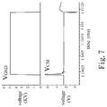
- FIG. 7 shows conventional waveform of the transient common noise V GND and interferences of V CM when no high speed detector is employed.
- FIG. 8 shows waveforms of the transient common noise V GND and interferences of V CM when the high speed detector of the present invention is employed.
- FIG. 9 shows conventional waveforms of the input signal DI, the output signal RO, the transient common noise V GND and interferences of V CM when no high speed detector is employed.
- FIG. 10 shows waveforms of the input signal DI, the output signal RO, the transient common noise V GND and interferences of V CM when the high speed detector of the present invention is employed.
- FIG. 11 shows conventional waveforms of the input signal DI and the output signal RO when no high speed detector is employed.
- FIG. 12 shows waveforms of the input signal DI and the output signal RO when the high speed detector of the present invention is employed.
- FIG. 2 shows a block diagram of a digital isolator module for high level common mode transient immunity in accordance with one embodiment of the present invention.
- the digital isolator module disclosed by the present invention comprises a transmitter circuit (TX) 200 , an isolation barrier 202 and a receiver circuit (RX) 204 .
- TX transmitter circuit
- RX receiver circuit
- the transmitter circuit (TX) 200 receives an input signal DI and generates a pair of differential signals, wherein the transmitter circuit 200 is electrically connected to a first ground voltage level V ss1 .
- the isolation barrier 202 is configured between the transmitter circuit 200 and the receiver circuit (RX) 204 , comprising two input ends for receiving and coupling the pair of differential signals from the transmitter circuit 200 .
- the isolation barrier 202 is composed of a first capacitor C 1 and a second capacitor C 2 which are connected in parallel. Each of the first capacitor C 1 and the second capacitor C 2 is connected between an output end of the transmitter circuit 200 and an input end of the receiver circuit 204 . Through the two output ends of the isolation barrier 202 , a pair of coupled signals are generated and served as inputs to the receiver side.
- the receiver circuit 204 which is being connected with the isolation barrier 202 is aimed to receive the pair of coupled signals from the isolation barrier 202 and to accordingly generate an output signal RO.
- the receiver circuit 204 is electrically connected to a second ground voltage level V ss2 and comprises a high speed detector 241 , a demodulator 243 and a resistance set.
- the resistance set comprises a first resistor R CM1 and a second resistor R CM2 which are connected in parallel.
- Each of the first resistor R CM1 and the second resistor R CM2 is connected between an input end of the demodulator 243 and the high speed detector 241 .
- Two first ends of the resistance set R CM1 , R CM2 are respectively connected to the two output ends of the isolation barrier 202 , as indicated by node “INP” and “INN” as shown in FIG. 2 .
- two second ends of the resistance set R CM1 , R CM2 are jointed and connected to an input end, being also the output end of the high speed detector 241 , as indicated by “V CM ” as shown in FIG. 2 .
- the demodulator 243 is connected with nodes “INP” and “INN” for receiving the coupled signals and generating the output signal RO.
- FIG. 3 shows a waveform of the transient common noise V GND comprising a rising edge and a falling edge
- the accordingly induced current I CM owing to the transient common noise V GND is indicated by the arrows. From these two figures shown, it is obvious that when the transient common noise V GND is increasing and at a rising edge, the induced current I CM will be generated and injected into the receiver circuit 204 as indicated by the solid line.
- the proposed isolator circuit structure of the present invention is aimed to stabilize the common mode voltage levels at both the nodes of INP and INN, such that the demodulator 243 can perform normally and correctly for outputting the output signal RO.
- the demodulator 243 can be an On-Off Keying (OOK) demodulator or the like.
- OOK On-Off Keying
- the high speed detector 241 detects a voltage signal of its input end i.e. node of V CM so as to determine if a compensation current is provided.
- the compensation current can be either a sink current or a source current, depending on the induced current I CM to be generated and to be injected from the TX side to the RX side, or from the RX side to the TX side.
- FIG. 5 shows a block diagram of the high speed detector in accordance with one embodiment of the present invention.
- the high speed detector 241 comprises a detecting circuit 52 and a current source circuit 54 .
- the detecting circuit 52 further comprises a source type transient control unit 522 and a sink type transient control unit 524 .
- the current source circuit 54 further comprises a source type current source 542 and a sink type current source 544 .
- An output end of the source type transient control unit 522 is connected to the source type current source 542 , and an output end of the sink type transient control unit 524 is connected to the sink type current source 544 , such that the source type current source 542 can be controlled relatively by its corresponding source type transient control unit 522 so as to provide a source current.
- the sink type current source 544 can be controlled relatively by its corresponding sink type transient control unit 524 so as to provide a sink current.
- the said source current and said sink current are referred as the previously mentioned compensation current.
- FIG. 6 shows a detailed illustration of the circuit diagram of the high speed detector in accordance with one embodiment of the present invention as shown in FIG. 5 .
- the source type transient control unit 522 further comprises an operational transconductance amplifier OTA, a third resistor R 3 and a fourth resistor R 4 .
- the third resistor R 3 is connected between ground and the fourth resistor R 4 .
- the fourth resistor R 4 is further connected to the input end, being also the output end of the high speed detector.
- the input end of the high speed detector and an output end of the high speed detector are common, i.e. the foregoing node of V CM .
- the operational transconductance amplifier OTA Two input ends of the operational transconductance amplifier OTA is respectively connected to a reference voltage signal V REF and a jointed end of the third resistor R 3 and the fourth resistor R 4 . And, an output end of the operational transconductance amplifier OTA is connected to the source type current source 542 for controlling the source type current source 542 and generating a source current.
- the source type current source 542 can be implemented as a P type Metal Oxide Semiconductor Field Effect Transistor (MOSFET).
- the sink type transient control unit 524 may further comprise a fifth resistor R 5 and a first transistor M 1 .
- the first transistor M 1 can be implemented as an N type Metal Oxide Semiconductor Field Effect Transistor (MOSFET).
- the fifth resistor R 5 is connected between ground, the third resistor R 3 and a source terminal of the first transistor M 1 .
- a gate terminal and a drain terminal of the first transistor M 1 are commonly connected to the input/output end of the high speed detector, and the source terminal of the first transistor M 1 is connected to the sink type current source 544 for controlling the sink type current source 544 and generating a sink current.
- the sink type current source 544 can be implemented as an N type Metal Oxide Semiconductor Field Effect Transistor (MOSFET).
- the source type current source 542 and the sink type current source 544 are connected in series between the high voltage level V cc and ground.
- a source terminal of the source type current source 542 is connected to the high voltage level V cc and a gate terminal of the source type current source 542 is connected to the output end of the operational transconductance amplifier OTA.
- a source terminal of the sink type current source 544 is connected to ground.
- a gate terminal of the sink type current source 544 is connected to the source terminal of the first transistor M 1 to receive control from the sink type transient control unit 524 , and drain terminals of the sink type current source 544 and the source type current source 542 are commonly connected as an output end of the current source circuit 54 and also to the input/output end of the high speed detector 241 .
- the induced current I CM when the transient common noise V GND is generated and is at its falling edge, the induced current I CM will be generated and flowing back to the transmitter circuit 200 . Under such circumstances, voltage level of V CM will start to drop instantly. At this time, the high speed detector 241 detects the declined voltage level of V CM and the source type transient control unit 522 is turned on, resulting in an ON path of the source type current source 542 and forming the source current. As such, the induced current I CM which has been flowing back to the transmitter circuit is able to be compensated due to the generated source current, such that the common mode voltage levels at both the nodes of INP and INN will be stabilized as well.
- FIG. 7 shows conventional waveforms of the transient common noise V GND and interferences of V CM when no high speed detector is employed
- FIG. 8 shows waveforms of the transient common noise V GND and interferences of V CM when the high speed detector of the present invention is employed.
- the transient common noise V GND is equal to a voltage of (V ss1 ⁇ V ss2 ), which was raised up to 5 KV from 0V from 1.1 ms to 1.10001 ms, and lowered down to 0V from 5 KV from 1.101 ms to 1.10101 ms.
- FIG. 9 shows conventional waveforms of the input signal DI, the output signal RO, the transient common noise V GND and interferences of V CM when no high speed detector is employed
- FIG. 10 shows waveforms of the input signal DI, the output signal RO, the transient common noise V GND and interferences of V CM when the high speed detector of the present invention is employed.
- the transient common noise V GND is equal to a voltage of (V ss1 ⁇ V ss2 ).
- FIG. 11 shows conventional waveforms of the input signal DI and the output signal RO when no high speed detector is employed
- FIG. 12 shows waveforms of the input signal DI and the output signal RO when the high speed detector of the present invention is employed.
- the propagation delays reaction time from DI to RO
- the transient response from low to high is 32.25 ns
- the transient response from high to low is 32.64 ns
- the transient response from low to high is 32.53 ns
- the transient response from high to low is 32.25 ns.
- the proposed digital isolator module of the present invention is characterized by utilizing a high speed detecting mechanism, which is able to sophisticatedly control both a source type current source and a sink type current source to operate, depending on a rise or decline of the transient common noise generated between two ground voltages.
- a compensation current being either a source current or a sink current can be provided to suppress the inferences being induced, and to stabilize the common mode voltages.
- the present invention is believed as beneficial to controlling voltage level stability and robustness of output voltages and thus meanwhile assuring data transmission accuracy.
- the present invention when compared to the prior arts, it is obvious that the present invention apparently shows much more effective performances than before.
- the present invention is instinct, effective and highly competitive for IC technology and industries in the market nowadays, whereby having extraordinary availability and competitiveness for future industrial developments and being in condition for early allowance.
Landscapes
- Engineering & Computer Science (AREA)
- Computer Networks & Wireless Communication (AREA)
- Signal Processing (AREA)
- Computer Hardware Design (AREA)
- Physics & Mathematics (AREA)
- Computing Systems (AREA)
- General Engineering & Computer Science (AREA)
- Mathematical Physics (AREA)
- Dc Digital Transmission (AREA)
- Noise Elimination (AREA)
- Transmitters (AREA)
Abstract
A digital isolator module for high level common mode transient immunity is provided, comprising a transmitter circuit (TX), a receiver circuit (RX) and an isolation barrier which is connected there in between, wherein the transmitter circuit is electrically connected to a first ground voltage level and the receiver circuit is electrically connected to a second ground voltage level. The receiver circuit further comprises a resistance set, a high speed detector and a demodulator. By employing the proposed circuit diagram of the invention, interferences occurring at the common mode are suppressed and an RX output signal is synchronized with its input signal without having propagation delay.
Description
The present invention is related to an isolation circuit, and more particularly to a digital isolator module which is employed for high level common mode transient immunity while ensuring reliable data transmission without propagation delay.
As we know, isolation circuits are the interface circuits that provide galvanic isolation between two communicating blocks, for example, a transmitter circuit (TX) and a receiver circuit (RX). Such isolation circuits are required to eliminate avoidable ground loops, and also to protect high voltage sensitive circuits. These circuits ensure electric insulation and signal isolation between the circuits, ensuring reliable data transmission between the two circuits, isolating the signal from fast transient common mode noise. In applications where common mode noise can be expected and human interactions are inevitable (e.g., cardiograph), then the isolation circuits act as an interface, ensuring safety and reliability. In several industrial applications which are susceptible to electrical surges, fast transients and high noise floors, isolation circuits have been widely used for safety and reliability.
Please refer to FIG. 1 , which shows a schematic drawing of a conventional isolation circuit architecture, wherein the two communicating blocks TX 10 and RX 20 are respectively connected to a ground voltage Vss1 and Vss2. The isolation circuit is aimed to isolate these two ground voltages Vss1 and Vss2 apart. As known, DI is an input of the isolation circuit and RO is its output. In the transmission proceeding progress, at first, DI is input to control the TX 10 to generate differential signals. An isolation capacitance pair 22 is configured between the TX 10 and the RX 20 for coupling the signals from the transmitter side to the receiver side, such that the RX 20 outputs the output signal RO. In general, a voltage level of the input signal DI should be followed by the voltage level of the output signal RO. Nevertheless, transmission errors always occur due to a transient common noise VGND generated between these two ground voltages Vss1 and Vss2. For example, a spike, electrical loop between two ground voltages, or any systematic issues are the commonly known factors. Also, since the conventional RX scheme circuits are not designed to be able to afford and tolerate high VGND voltages, the signal transmission has inevitably gone wrong owing to such the transient common noise, and the performance of the isolation circuit to convey signals suffers a lot due to common mode current transients.
As such, in order to ensure the robustness and reliability of the data transmission, common mode transient immunity (CMTI) has been expected to be improved as high as possible. And efforts to improve isolation circuit performances are ongoing. For example, An U.S. Pat. No. 9,257,836 discloses a common transient suppression circuit coupled to a receive circuit to suppress transients in signals received by the receive circuit that were transmitted from a transmit side of the isolation barrier using optical, magnetic, inductive, or other mechanisms. However, it was observed that its data transmission process encounters propagation delay issues since a certain delay circuit must be involved in such design. Another U.S. patent 2017/0201399 discloses a common mode transient immunity circuit for opto-isolator emulation, which includes a voltage clamping circuit coupled to receive an input signal and to provide a clamped signal, an oscillator coupled to receive the clamped signal and to provide the differential output signals, and a common mode transient immunity (CMTI) circuit that couples respective first terminals of the first and second capacitors to a lower rail responsive to the clamped signal being low. Nevertheless, the aforesaid circuits were configured in the data transmitting side, and can only be taken into consideration and applied to limited conditions, i.e. when there was a decline in common mode noise or ground noise leading to induced current to be pulled towards a transmitter during the negative (also known as a falling) edge of the transient. As a result, it is believed that such design is still in lack of extensive utility and can not be widely used.
Under such circumstances, it, in view of all, should be apparent and obvious that there is indeed an urgent need for the professionals in the field for a novel and inventive isolation circuit to be developed so as to achieve the purposes of not only accurate data transmission process but also extraordinarily high common mode transient immunity.
In order to overcome the above mentioned disadvantages, one major objective in accordance with the present invention is provided for a novel and creative isolation circuit which can successfully solves the problems of prior arts and achieve precise data transmission result as well as high level common mode transient immunity.
Another objective in accordance with the present invention is provided for a novel digital isolator module, in which a high speed detecting mechanism is employed. By integrating a high speed detecting circuit therewith the conventional receiver side, a common mode voltage level at the input of the receiver side can be stabilized, such that its output signal RO can be synchronized with the input signal DI and no propagation delay is observed to be occurred.
And yet another objective in accordance with the present invention is provided for a digital isolator module for high level common mode transient immunity, in which the all new high speed detecting circuit scheme is proposed to have not only a source type transient control but also a sink type transient control. Depending on the waveform and voltage level (i.e. a rise or a decline) of the transient common noise generated between two respective grounds, either a source current or a sink current will be generated to compensate the interfered current and to maintain the system robustness and common mode voltage level of the circuit.
For achieving the above mentioned objectives, the present invention provides a digital isolator module for high level common mode transient immunity, comprising: a transmitter circuit, coupled to receive an input signal and generate a pair of differential signals; an isolation barrier, having two input ends for receiving and coupling the pair of differential signals and two output ends for accordingly generating a pair of coupled signals; and a receiver circuit, connected with the isolation barrier to receive the pair of coupled signals and generate an output signal.
In one embodiment, the isolation barrier comprises a first capacitor and a second capacitor, which are connected in parallel. And, each of the first capacitor and the second capacitor is connected between an output end of the transmitter circuit and an input end of the receiver circuit.
In a preferred embodiment of the present invention, the receiver circuit further comprises a resistance set, a high speed detector and a demodulator, wherein two first ends of the resistance set are respectively connected to the two output ends of the isolation barrier and two second ends of the resistance set are jointed and connected to an input end, being also the output end of the high speed detector. The demodulator is connected with the first ends of the resistance set so as to generate the output signal.
In one embodiment, the resistance set may comprise a first resistor and a second resistor, which are connected in parallel. And each of the first resistor and the second resistor is connected between an input end of the demodulator and the high speed detector.
According to the present invention, the transmitter circuit is electrically connected to a first ground voltage level Vss1 and the receiver circuit is electrically connected to a second ground voltage level Vss2. As such, when there is a transient common noise VGND which is generated between the first ground voltage level Vss1 and the second ground voltage level Vss2, the high speed detector detects a voltage signal of the input end, being also the output end of the high speed detector (i.e. VCM) for determining if a compensation current is provided such that interferences occurring at the input end, being also the output end of the high speed detector are suppressed. In addition, the output signal can be synchronized with the input signal without propagation delay.
Therefore, in a preferred embodiment of the present invention, the high speed detector is designed to comprise a detecting circuit and a current source circuit, wherein the detecting circuit further comprises a source type transient control unit and a sink type transient control unit, and the current source circuit further comprises a source type current source and a sink type current source.
An output end of the source type transient control unit is connected to the source type current source. An output end of the sink type transient control unit is connected to the sink type current source. By such designed arrangements, the source type current source is controlled by the source type transient control unit so as to provide a source current. In a preferred embodiment of the present invention, the source type current source can be implemented as a P type Metal Oxide Semiconductor Field Effect Transistor (PMOS). In another aspect, the sink type current source is controlled by the sink type transient control unit so as to provide a sink current. In a preferred embodiment of the present invention, the sink type current source can be implemented as an N type Metal Oxide Semiconductor Field Effect Transistor (NMOS) In other words, when the transient common noise is at a rising edge, then the sink type transient control unit controls the sink type current source, so the compensation current is the generated sink current.
Similarly, when the transient common noise is at a falling edge, then the source type transient control unit controls the source type current source, so the compensation current is the generated source current.
As a result, it is believed that the source current and/or the sink current can be sophisticated provided so as to compensate an interfered current at VCM and to stabilize the common mode voltage level of the circuit. And thus, the system robustness, common mode voltage level of the circuit, and high level common mode transient immunity are accomplished through the present invention.
Based on the above, it has been proved that the present invention is well designed and indeed discloses a novel digital isolator module for high level common mode transient immunity. The whole new schemes can be employed in a receiving circuit (RX) architecture, and has been verified to get high level common mode transient immunity (CMTI), better system robustness and precise data transmission results. Thus, it is believed that the present invention is advantageous of having excellent control stability over system levels as well as maintaining precise control ability to the isolation circuits while compared to the prior arts.
These and other objectives of the present invention will become obvious to those of ordinary skill in the art after reading the following detailed description of preferred embodiments.
It is to be understood that both the foregoing general description and the following detailed description are exemplary, and are intended to provide further explanation of the invention as claimed.
The accompanying drawings are included to provide a further understanding of the invention, and are incorporated in and constitute a part of this specification. The drawings illustrate embodiments of the invention and, together with the description, serve to explain the principles of the invention. In the drawings:
Reference will now be made in detail to the preferred embodiments of the present invention, examples of which are illustrated in the accompanying drawings. Wherever possible, the same reference numbers are used in the drawings and the description to refer to the same or like parts.
The embodiments described below are illustrated to demonstrate the technical contents and characteristics of the present invention and to enable the persons skilled in the art to understand, make, and use the present invention. However, it shall be noticed that, it is not intended to limit the scope of the present invention. Therefore, any equivalent modification or variation according to the spirit of the present invention is to be also included within the scope of the present invention.
Please refer to FIG. 2 , which shows a block diagram of a digital isolator module for high level common mode transient immunity in accordance with one embodiment of the present invention. As shown in FIG. 2 , the digital isolator module disclosed by the present invention comprises a transmitter circuit (TX) 200, an isolation barrier 202 and a receiver circuit (RX) 204.
The transmitter circuit (TX) 200 receives an input signal DI and generates a pair of differential signals, wherein the transmitter circuit 200 is electrically connected to a first ground voltage level Vss1.
The isolation barrier 202 is configured between the transmitter circuit 200 and the receiver circuit (RX) 204, comprising two input ends for receiving and coupling the pair of differential signals from the transmitter circuit 200. According to the embodiment of the present invention, the isolation barrier 202 is composed of a first capacitor C1 and a second capacitor C2 which are connected in parallel. Each of the first capacitor C1 and the second capacitor C2 is connected between an output end of the transmitter circuit 200 and an input end of the receiver circuit 204. Through the two output ends of the isolation barrier 202, a pair of coupled signals are generated and served as inputs to the receiver side.
The receiver circuit 204 which is being connected with the isolation barrier 202 is aimed to receive the pair of coupled signals from the isolation barrier 202 and to accordingly generate an output signal RO. According to the embodiment of the present invention, the receiver circuit 204 is electrically connected to a second ground voltage level Vss2 and comprises a high speed detector 241, a demodulator 243 and a resistance set.
According to the embodiment of the present invention, the resistance set comprises a first resistor RCM1 and a second resistor RCM2 which are connected in parallel. Each of the first resistor RCM1 and the second resistor RCM2 is connected between an input end of the demodulator 243 and the high speed detector 241.
Two first ends of the resistance set RCM1, RCM2 are respectively connected to the two output ends of the isolation barrier 202, as indicated by node “INP” and “INN” as shown in FIG. 2 . On the other hand, two second ends of the resistance set RCM1, RCM2 are jointed and connected to an input end, being also the output end of the high speed detector 241, as indicated by “VCM” as shown in FIG. 2 . The demodulator 243 is connected with nodes “INP” and “INN” for receiving the coupled signals and generating the output signal RO.
Since a transient common noise VGND is inevitably generated between the first ground voltage level Vss1 and the second ground voltage level Vss2, an induced current ICM will thus be generated either from the transmitting side (TX) flowing into the receiving side (RX), or from the receiving side (RX) flowing into the transmitting side (TX). Please find referring at the same time to FIG. 3 and FIG. 4 , in which FIG. 3 shows a waveform of the transient common noise VGND comprising a rising edge and a falling edge, while in FIG. 4 the accordingly induced current ICM owing to the transient common noise VGND is indicated by the arrows. From these two figures shown, it is obvious that when the transient common noise VGND is increasing and at a rising edge, the induced current ICM will be generated and injected into the receiver circuit 204 as indicated by the solid line.
In the same manners, when the transient common noise VGND is declined and at a falling edge, then the induced current ICM will be generated and flowing back to the transmitter circuit 200 as indicated by the dashed line. On account of these situations, the voltage levels at the nodes “INP” and “INN” are disturbed and become variable, whereby affect the accuracy of the output signal RO. As a result, the proposed isolator circuit structure of the present invention is aimed to stabilize the common mode voltage levels at both the nodes of INP and INN, such that the demodulator 243 can perform normally and correctly for outputting the output signal RO.
In one embodiment, the demodulator 243, for example, can be an On-Off Keying (OOK) demodulator or the like. For people who are skilled in the art and having understandings and technical backgrounds to the present invention, it would be allowed for them to make various modifications or changes depending on different circuit regulations and/or specifications without departing from the scope of the invention. That is to say, the present invention is certainly not limited thereto.
In the following paragraphs, it draws our attention that how the present invention works to stabilize the common mode voltage levels at both the nodes of INP and INN. The main technical features of the proposed circuit diagrams disclosed by the present invention are that, the high speed detector 241 detects a voltage signal of its input end i.e. node of VCM so as to determine if a compensation current is provided. According to a preferred embodiment of the present invention, the compensation current can be either a sink current or a source current, depending on the induced current ICM to be generated and to be injected from the TX side to the RX side, or from the RX side to the TX side.
Please refer to FIG. 5 , which shows a block diagram of the high speed detector in accordance with one embodiment of the present invention. As shown in FIG. 5 , the high speed detector 241 comprises a detecting circuit 52 and a current source circuit 54.
The detecting circuit 52 further comprises a source type transient control unit 522 and a sink type transient control unit 524. And, the current source circuit 54 further comprises a source type current source 542 and a sink type current source 544.
An output end of the source type transient control unit 522 is connected to the source type current source 542, and an output end of the sink type transient control unit 524 is connected to the sink type current source 544, such that the source type current source 542 can be controlled relatively by its corresponding source type transient control unit 522 so as to provide a source current.
In a similar methodology, the sink type current source 544 can be controlled relatively by its corresponding sink type transient control unit 524 so as to provide a sink current. The said source current and said sink current are referred as the previously mentioned compensation current.
In another aspect, the sink type transient control unit 524 may further comprise a fifth resistor R5 and a first transistor M1. According to the embodiment of the present invention, the first transistor M1 can be implemented as an N type Metal Oxide Semiconductor Field Effect Transistor (MOSFET).
The fifth resistor R5 is connected between ground, the third resistor R3 and a source terminal of the first transistor M1. A gate terminal and a drain terminal of the first transistor M1 are commonly connected to the input/output end of the high speed detector, and the source terminal of the first transistor M1 is connected to the sink type current source 544 for controlling the sink type current source 544 and generating a sink current. According to the embodiment of the present invention, the sink type current source 544 can be implemented as an N type Metal Oxide Semiconductor Field Effect Transistor (MOSFET).
In addition, the source type current source 542 and the sink type current source 544 are connected in series between the high voltage level Vcc and ground. A source terminal of the source type current source 542 is connected to the high voltage level Vcc and a gate terminal of the source type current source 542 is connected to the output end of the operational transconductance amplifier OTA.
A source terminal of the sink type current source 544 is connected to ground. A gate terminal of the sink type current source 544 is connected to the source terminal of the first transistor M1 to receive control from the sink type transient control unit 524, and drain terminals of the sink type current source 544 and the source type current source 542 are commonly connected as an output end of the current source circuit 54 and also to the input/output end of the high speed detector 241.
As a result, with referring to FIG. 3 and FIG. 4 at the same time, when the transient common noise VGND is generated and is at its rising edge, the induced current ICM will be generated and injected into the receiver circuit 204. Under such circumstances, voltage level of VCM will start to rise instantly. At this time, the high speed detector 241 detects the raised voltage level of VCM and the sink type transient control unit 524 would be turned on, resulting in an ON path of the sink type current source 544. As such, the induced current ICM which has been injected into the receiver circuit 204 is able to sink to ground through the path owing to the sink type current source 544, forming the sink current. By such designs, interferences occurring at the input/output end of the high speed detector, i.e. VCM are effectively suppressed. In addition, common mode voltage levels at both the nodes of INP and INN are stabilized.
In the same methodology, when the transient common noise VGND is generated and is at its falling edge, the induced current ICM will be generated and flowing back to the transmitter circuit 200. Under such circumstances, voltage level of VCM will start to drop instantly. At this time, the high speed detector 241 detects the declined voltage level of VCM and the source type transient control unit 522 is turned on, resulting in an ON path of the source type current source 542 and forming the source current. As such, the induced current ICM which has been flowing back to the transmitter circuit is able to be compensated due to the generated source current, such that the common mode voltage levels at both the nodes of INP and INN will be stabilized as well.
In the following sections, the present invention will now be verified with experimental simulation results provided below to show that, by employing the proposed digital isolator module for high level common mode transient immunity of the present invention scheme, not only the interferences occurring at VCM can be successfully suppressed, but also the output signal RO is accurate and synchronized with the input signal DI without any propagation delay.
Moreover, FIG. 9 shows conventional waveforms of the input signal DI, the output signal RO, the transient common noise VGND and interferences of VCM when no high speed detector is employed, while FIG. 10 shows waveforms of the input signal DI, the output signal RO, the transient common noise VGND and interferences of VCM when the high speed detector of the present invention is employed. In these figures, the transient common noise VGND is equal to a voltage of (Vss1−Vss2).
In FIG. 9 , it was observed that the output signal RO was not identical to the input signal DI. Also, interferences of VCM were not eliminated. However, compared to the waveforms as shown in FIG. 10 when employing the present invention, it is successfully proved that the output signal RO is improved to follow and being identical to the input signal DI. At the same time, interferences of VCM are effectively suppressed as well such that a voltage level of VCM can be maintained stably at 2.4V owing to the novel high speed detector employed by the present invention.
Furthermore, FIG. 11 shows conventional waveforms of the input signal DI and the output signal RO when no high speed detector is employed, while FIG. 12 shows waveforms of the input signal DI and the output signal RO when the high speed detector of the present invention is employed. As we compare these two simulation results, we find that the propagation delays (reaction time from DI to RO) are similar. In FIG. 9 , the transient response from low to high is 32.25 ns, and the transient response from high to low is 32.64 ns. While in FIG. 10 , the transient response from low to high is 32.53 ns, and the transient response from high to low is 32.25 ns. From these simulation results, it is apparent that the propagation delays (reaction time from DI to RO) are similar, and no increase of propagation delay will be caused due to the proposed high speed detector the present invention utilized. This is mostly because the high speed detector disclosed by the present invention is not designed and configured in the main data transmission path along the transmitting side TX to the receiving side RX. As a result, the present invention is advantageous of maintaining excellent data transmission accuracy and making no further data propagation delay.
Therefore, based on at least one proof provided above, it is believed that the proposed digital isolator module of the present invention is characterized by utilizing a high speed detecting mechanism, which is able to sophisticatedly control both a source type current source and a sink type current source to operate, depending on a rise or decline of the transient common noise generated between two ground voltages. Under such circumstances, a compensation current being either a source current or a sink current can be provided to suppress the inferences being induced, and to stabilize the common mode voltages. As such, by employing the proposed circuit diagram, the present invention is believed as beneficial to controlling voltage level stability and robustness of output voltages and thus meanwhile assuring data transmission accuracy.
As a result, when compared to the prior arts, it is obvious that the present invention apparently shows much more effective performances than before. In addition, it is believed that the present invention is instinct, effective and highly competitive for IC technology and industries in the market nowadays, whereby having extraordinary availability and competitiveness for future industrial developments and being in condition for early allowance.
It will be apparent to those skilled in the art that various modifications and variations can be made to the present invention without departing from the scope or spirit of the invention. In view of the foregoing, it is intended that the present invention cover modifications and variations of this invention provided they fall within the scope of the invention and its equivalent.
Claims (12)
1. A digital isolator module for high level common mode transient immunity, comprising:
a transmitter circuit, having an input end connected to an input signal and generating a pair of output differential signals from said input signal, wherein said transmitter circuit is electrically connected to a first ground voltage level;
an isolation barrier, having two input ends connected to said output differential signals of said transmitter circuit and two output ends;
a receiver circuit, having a pair of inputs connected with said two output ends of said isolation barrier and generating an output signal, wherein said receiver circuit is electrically connected to a second ground voltage level and said receiver circuit comprises a resistance set, a high speed detector and a demodulator, two first ends of said resistance set are respectively connected to said two output ends of said isolation barrier and two second ends of said resistance set are jointed and connected to an input end of said high speed detector, said input end and an output end of said high speed detector is commonly jointed, said demodulator is connected with said two first ends of said resistance set so as to generate said output signal.
2. The digital isolator module for high level common mode transient immunity according to claim 1 , wherein said isolation barrier comprises a first capacitor and a second capacitor which are connected in parallel, each of said first capacitor and said second capacitor is connected between an output end of said transmitter circuit and one of said inputs of said receiver circuit.
3. The digital isolator module for high level common mode transient immunity according to claim 1 , wherein said resistance set comprises a first resistor and a second resistor which are connected in parallel, each of said first resistor and said second resistor is connected between an input end of said demodulator and said high speed detector.
4. The digital isolator module for high level common mode transient immunity according to claim 1 , wherein said high speed detector comprises a detecting circuit and a current source circuit, said detecting circuit further comprises a source type transient control unit and a sink type transient control unit, said current source circuit further comprises a source type current source and a sink type current source, an output end of each of said source type transient control unit and said sink type transient control unit is respectively connected to said source type current source and said sink type current source for controlling said source type current source and said sink type current source so as to provide said compensation current.
5. The digital isolator module for high level common mode transient immunity according to claim 4 , wherein said source type transient control unit comprises an operational transconductance amplifier, a third resistor and a fourth resistor, said third resistor is connected between ground and said fourth resistor which is further connected to said input end and said output end of said high speed detector, two input ends of said operational transconductance amplifier is respectively connected to a reference voltage signal and a jointed end of said third resistor and said fourth resistor, and an output end of said operational transconductance amplifier is connected to said source type current source.
6. The digital isolator module for high level common mode transient immunity according to claim 5 , wherein said source type current source is a P type Metal Oxide Semiconductor Field Effect Transistor (MOSFET).
7. The digital isolator module for high level common mode transient immunity according to claim 4 , wherein said sink type transient control unit further comprises a fifth resistor and a first transistor, said fifth resistor is connected between ground and a source terminal of said first transistor, a gate terminal and a drain terminal of said first transistor is connected to said input end and said output end of said high speed detector, and said source terminal of said first transistor is connected to said sink type current source.
8. The digital isolator module for high level common mode transient immunity according to claim 7 , wherein said sink type current source is an N type Metal Oxide Semiconductor Field Effect Transistor (MOSFET).
9. The digital isolator module for high level common mode transient immunity according to claim 7 , wherein said first transistor is an N type Metal Oxide Semiconductor Field Effect Transistor (MOSFET).
10. The digital isolator module for high level common mode transient immunity according to claim 4 , wherein said source type current source and said sink type current source are respectively a P type Metal Oxide Semiconductor Field Effect Transistor and a N type Metal Oxide Semiconductor Field Effect Transistor which are connected in series between a high voltage level and ground, a drain terminal of said sink type current source and said source type current source is commonly connected to an output end of said current source circuit.
11. The digital isolator module for high level common mode transient immunity according to claim 10 , wherein a source terminal of said source type current source is connected to said high voltage level and a gate terminal of said source type current source is connected to an output end of said source type transient control unit.
12. The digital isolator module for high level common mode transient immunity according to claim 10 , wherein a source terminal of said sink type current source is connected to ground and a gate terminal of said sink type current source is connected to an output end of said sink type transient control unit.
Priority Applications (3)
| Application Number | Priority Date | Filing Date | Title |
|---|---|---|---|
| US16/515,213 US10659173B1 (en) | 2019-07-18 | 2019-07-18 | Digital isolator module for high level common mode transient immunity |
| CN201910863633.8A CN110729994B (en) | 2019-07-18 | 2019-09-12 | Digital isolator for resisting high-level common mode transient interference |
| TW108136568A TWI770428B (en) | 2019-07-18 | 2019-10-09 | Digital isolator module for high level common mode transient immunity |
Applications Claiming Priority (1)
| Application Number | Priority Date | Filing Date | Title |
|---|---|---|---|
| US16/515,213 US10659173B1 (en) | 2019-07-18 | 2019-07-18 | Digital isolator module for high level common mode transient immunity |
Publications (1)
| Publication Number | Publication Date |
|---|---|
| US10659173B1 true US10659173B1 (en) | 2020-05-19 |
Family
ID=69218197
Family Applications (1)
| Application Number | Title | Priority Date | Filing Date |
|---|---|---|---|
| US16/515,213 Active US10659173B1 (en) | 2019-07-18 | 2019-07-18 | Digital isolator module for high level common mode transient immunity |
Country Status (3)
| Country | Link |
|---|---|
| US (1) | US10659173B1 (en) |
| CN (1) | CN110729994B (en) |
| TW (1) | TWI770428B (en) |
Cited By (11)
| Publication number | Priority date | Publication date | Assignee | Title |
|---|---|---|---|---|
| CN112947182A (en) * | 2021-02-05 | 2021-06-11 | 电子科技大学 | Control circuit for improving common-mode transient anti-interference degree of negative transconductance oscillator |
| CN113452364A (en) * | 2021-07-22 | 2021-09-28 | 苏州纳芯微电子股份有限公司 | Digital isolator |
| US11146341B1 (en) | 2020-09-29 | 2021-10-12 | Infineon Technologies Ag | Capacitive data transmission over a galvanic isolation |
| CN113572469A (en) * | 2021-07-29 | 2021-10-29 | 苏州纳芯微电子股份有限公司 | Digital isolator with pseudo-differential structure |
| US11706056B2 (en) | 2021-03-22 | 2023-07-18 | Infineon Technologies Ag | Capacitive data transmission over a galvanic isolation |
| WO2023168149A1 (en) * | 2022-03-04 | 2023-09-07 | Allegro Microsystems, Llc | Common mode transient suppression |
| EP4156516A4 (en) * | 2020-05-20 | 2023-11-01 | Suzhou Novosense Microelectronics Co., Ltd. | Protection circuit for common-mode transient immunity of digital isolator |
| CN116990599A (en) * | 2023-07-10 | 2023-11-03 | 深圳锐来博微电子有限公司 | Common mode noise detection circuit and digital isolator |
| EP4156512A4 (en) * | 2020-05-20 | 2023-11-08 | Suzhou Novosense Microelectronics Co., Ltd. | Differential signal amplification circuit, digital isolator, and receiver |
| CN117233513A (en) * | 2023-11-10 | 2023-12-15 | 厦门腾睿微电子科技有限公司 | System and method for testing common mode transient immunity of driving chip |
| CN117254682A (en) * | 2023-11-20 | 2023-12-19 | 成都芯翼科技有限公司 | Anti-interference voltage conversion circuit |
Families Citing this family (4)
| Publication number | Priority date | Publication date | Assignee | Title |
|---|---|---|---|---|
| CN113419595B (en) * | 2021-07-22 | 2022-03-18 | 苏州纳芯微电子股份有限公司 | Digital isolator and common mode interference suppression circuit thereof |
| CN114002589A (en) * | 2021-11-02 | 2022-02-01 | 苏州纳芯微电子股份有限公司 | Digital isolation unit fault detection method and detection system |
| CN114826243B (en) * | 2022-06-27 | 2022-09-20 | 宜矽源半导体南京有限公司 | Isolator receiving end input circuit with high transient common mode rejection |
| CN116705710B (en) * | 2023-06-13 | 2024-02-20 | 北京中科格励微科技有限公司 | Airtight digital isolator based on wafer reconstruction and manufacturing method |
Citations (9)
| Publication number | Priority date | Publication date | Assignee | Title |
|---|---|---|---|---|
| US20050272378A1 (en) * | 2004-06-03 | 2005-12-08 | Timothy Dupuis | Spread spectrum isolator |
| US20060073150A1 (en) | 2001-09-06 | 2006-04-06 | Mary Faris | Nucleic acid and corresponding protein entitled STEAP-1 useful in treatment and detection of cancer |
| US20080315925A1 (en) * | 2007-06-25 | 2008-12-25 | Alfano Donald E | Isolator circuit including a voltage regulator |
| US20140062527A1 (en) * | 2012-09-04 | 2014-03-06 | Michael Mills | Isolation receiver |
| US20140169038A1 (en) * | 2012-12-13 | 2014-06-19 | Texas Instruments Incorporated | Digital isolator |
| US9257836B2 (en) | 2013-12-19 | 2016-02-09 | Silicon Laboratories Inc. | Suppression of transients in communications across an isolation barrier |
| US20160126724A1 (en) * | 2014-11-03 | 2016-05-05 | Analog Devices, Inc. | Signal isolator system with protection for common mode transients |
| US9553445B2 (en) | 2015-02-11 | 2017-01-24 | Rockwell Automation Asia Pacific Business Centre Pte. Ltd. | High-speed input circuit |
| US20170201399A1 (en) * | 2016-01-11 | 2017-07-13 | Texas Instruments Incorporated | Common Mode Transient Immunity Circuit For Opto-Isolator Emulation |
Family Cites Families (5)
| Publication number | Priority date | Publication date | Assignee | Title |
|---|---|---|---|---|
| US8451032B2 (en) * | 2010-12-22 | 2013-05-28 | Silicon Laboratories Inc. | Capacitive isolator with schmitt trigger |
| US9621383B1 (en) * | 2015-11-06 | 2017-04-11 | Monolithic Power Systems, Inc. | Digital isolator and the method thereof |
| CN106896281A (en) * | 2016-12-30 | 2017-06-27 | 北京航空航天大学 | A kind of method of testing of the transient state common mode inhibition parameter to numeral isolation class device |
| US10236878B1 (en) * | 2018-06-05 | 2019-03-19 | Texas Instruments Incorporated | Isolator device with common-mode voltage regulation |
| CN109387716A (en) * | 2018-10-31 | 2019-02-26 | 中国电子科技集团公司第五十八研究所 | Common mode transient state immunity to interference test based on digital isolator |
-
2019
- 2019-07-18 US US16/515,213 patent/US10659173B1/en active Active
- 2019-09-12 CN CN201910863633.8A patent/CN110729994B/en active Active
- 2019-10-09 TW TW108136568A patent/TWI770428B/en active
Patent Citations (9)
| Publication number | Priority date | Publication date | Assignee | Title |
|---|---|---|---|---|
| US20060073150A1 (en) | 2001-09-06 | 2006-04-06 | Mary Faris | Nucleic acid and corresponding protein entitled STEAP-1 useful in treatment and detection of cancer |
| US20050272378A1 (en) * | 2004-06-03 | 2005-12-08 | Timothy Dupuis | Spread spectrum isolator |
| US20080315925A1 (en) * | 2007-06-25 | 2008-12-25 | Alfano Donald E | Isolator circuit including a voltage regulator |
| US20140062527A1 (en) * | 2012-09-04 | 2014-03-06 | Michael Mills | Isolation receiver |
| US20140169038A1 (en) * | 2012-12-13 | 2014-06-19 | Texas Instruments Incorporated | Digital isolator |
| US9257836B2 (en) | 2013-12-19 | 2016-02-09 | Silicon Laboratories Inc. | Suppression of transients in communications across an isolation barrier |
| US20160126724A1 (en) * | 2014-11-03 | 2016-05-05 | Analog Devices, Inc. | Signal isolator system with protection for common mode transients |
| US9553445B2 (en) | 2015-02-11 | 2017-01-24 | Rockwell Automation Asia Pacific Business Centre Pte. Ltd. | High-speed input circuit |
| US20170201399A1 (en) * | 2016-01-11 | 2017-07-13 | Texas Instruments Incorporated | Common Mode Transient Immunity Circuit For Opto-Isolator Emulation |
Cited By (15)
| Publication number | Priority date | Publication date | Assignee | Title |
|---|---|---|---|---|
| EP4156516A4 (en) * | 2020-05-20 | 2023-11-01 | Suzhou Novosense Microelectronics Co., Ltd. | Protection circuit for common-mode transient immunity of digital isolator |
| EP4156512A4 (en) * | 2020-05-20 | 2023-11-08 | Suzhou Novosense Microelectronics Co., Ltd. | Differential signal amplification circuit, digital isolator, and receiver |
| US11146341B1 (en) | 2020-09-29 | 2021-10-12 | Infineon Technologies Ag | Capacitive data transmission over a galvanic isolation |
| CN112947182A (en) * | 2021-02-05 | 2021-06-11 | 电子科技大学 | Control circuit for improving common-mode transient anti-interference degree of negative transconductance oscillator |
| CN112947182B (en) * | 2021-02-05 | 2023-05-26 | 电子科技大学 | Control circuit for improving common mode transient anti-interference degree of negative transconductance oscillator |
| US11706056B2 (en) | 2021-03-22 | 2023-07-18 | Infineon Technologies Ag | Capacitive data transmission over a galvanic isolation |
| CN113452364A (en) * | 2021-07-22 | 2021-09-28 | 苏州纳芯微电子股份有限公司 | Digital isolator |
| CN113452364B (en) * | 2021-07-22 | 2022-12-23 | 苏州纳芯微电子股份有限公司 | Digital isolator |
| CN113572469A (en) * | 2021-07-29 | 2021-10-29 | 苏州纳芯微电子股份有限公司 | Digital isolator with pseudo-differential structure |
| WO2023168149A1 (en) * | 2022-03-04 | 2023-09-07 | Allegro Microsystems, Llc | Common mode transient suppression |
| CN116990599A (en) * | 2023-07-10 | 2023-11-03 | 深圳锐来博微电子有限公司 | Common mode noise detection circuit and digital isolator |
| CN117233513A (en) * | 2023-11-10 | 2023-12-15 | 厦门腾睿微电子科技有限公司 | System and method for testing common mode transient immunity of driving chip |
| CN117233513B (en) * | 2023-11-10 | 2024-01-30 | 厦门腾睿微电子科技有限公司 | System and method for testing common mode transient immunity of driving chip |
| CN117254682A (en) * | 2023-11-20 | 2023-12-19 | 成都芯翼科技有限公司 | Anti-interference voltage conversion circuit |
| CN117254682B (en) * | 2023-11-20 | 2024-03-12 | 成都芯翼科技有限公司 | Anti-interference voltage conversion circuit |
Also Published As
| Publication number | Publication date |
|---|---|
| CN110729994A (en) | 2020-01-24 |
| CN110729994B (en) | 2023-02-28 |
| TWI770428B (en) | 2022-07-11 |
| TW202105913A (en) | 2021-02-01 |
Similar Documents
| Publication | Publication Date | Title |
|---|---|---|
| US10659173B1 (en) | Digital isolator module for high level common mode transient immunity | |
| CN106961272B (en) | Common-mode transient immunity circuit for optical isolator simulation | |
| TWI506951B (en) | Signal transmitting circuit | |
| US9998301B2 (en) | Signal isolator system with protection for common mode transients | |
| US10536309B2 (en) | Demodulation of on-off-key modulated signals in signal isolator systems | |
| US7633312B2 (en) | Data transmission apparatus and a data receiving apparatus used for the same | |
| EP3734414B1 (en) | Signal detector | |
| US20080218238A1 (en) | Input signal detecting circuit | |
| US9396155B2 (en) | Envelope detection device and related communication device | |
| CN113452364B (en) | Digital isolator | |
| KR20010051033A (en) | Current driver circuit | |
| US10853295B2 (en) | Interface circuit and method for controlling switching circuit within interface circuit | |
| US20130342943A1 (en) | Input protection circuit | |
| CN113271095B (en) | Common-mode transient interference rejection circuit and modulation-demodulation circuit | |
| US11522505B2 (en) | Semiconductor integrated circuit and receiver device | |
| EP3809593B1 (en) | A low power receiver circuit for isolated data communications | |
| US7772853B2 (en) | Semiconductor device | |
| US10797704B2 (en) | Differential signal transfer systems and associated methods | |
| CN114696771A (en) | Common mode transient interference suppression circuit and isolator | |
| CN116783830A (en) | Transmitting circuit of controller area network CAN transceiver and CAN transceiver | |
| JP2022189009A (en) | Insulation communication system | |
| CN111937309A (en) | Detector circuit and system for transmitting digital signals in electrically isolated manner | |
| EP3157219B1 (en) | Demodulation of on-off modulated signals in signal isolator systems | |
| CN216699983U (en) | Modulation-demodulation circuit | |
| CN111095884B (en) | Signal output device |
Legal Events
| Date | Code | Title | Description |
|---|---|---|---|
| FEPP | Fee payment procedure |
Free format text: ENTITY STATUS SET TO UNDISCOUNTED (ORIGINAL EVENT CODE: BIG.); ENTITY STATUS OF PATENT OWNER: SMALL ENTITY |
|
| FEPP | Fee payment procedure |
Free format text: ENTITY STATUS SET TO SMALL (ORIGINAL EVENT CODE: SMAL); ENTITY STATUS OF PATENT OWNER: SMALL ENTITY |
|
| STCF | Information on status: patent grant |
Free format text: PATENTED CASE |
|
| MAFP | Maintenance fee payment |
Free format text: PAYMENT OF MAINTENANCE FEE, 4TH YR, SMALL ENTITY (ORIGINAL EVENT CODE: M2551); ENTITY STATUS OF PATENT OWNER: SMALL ENTITY Year of fee payment: 4 |